WO2012124204A1 - 制御プログラム開発支援装置、制御プログラム開発支援用プログラム及び記録媒体 - Google Patents
制御プログラム開発支援装置、制御プログラム開発支援用プログラム及び記録媒体 Download PDFInfo
- Publication number
- WO2012124204A1 WO2012124204A1 PCT/JP2011/074304 JP2011074304W WO2012124204A1 WO 2012124204 A1 WO2012124204 A1 WO 2012124204A1 JP 2011074304 W JP2011074304 W JP 2011074304W WO 2012124204 A1 WO2012124204 A1 WO 2012124204A1
- Authority
- WO
- WIPO (PCT)
- Prior art keywords
- unit
- port
- control program
- rack
- variable
- Prior art date
- Legal status (The legal status is an assumption and is not a legal conclusion. Google has not performed a legal analysis and makes no representation as to the accuracy of the status listed.)
- Ceased
Links
Images












Classifications
-
- G—PHYSICS
- G05—CONTROLLING; REGULATING
- G05B—CONTROL OR REGULATING SYSTEMS IN GENERAL; FUNCTIONAL ELEMENTS OF SUCH SYSTEMS; MONITORING OR TESTING ARRANGEMENTS FOR SUCH SYSTEMS OR ELEMENTS
- G05B19/00—Program-control systems
- G05B19/02—Program-control systems electric
- G05B19/04—Program control other than numerical control, i.e. in sequence controllers or logic controllers
- G05B19/042—Program control other than numerical control, i.e. in sequence controllers or logic controllers using digital processors
- G05B19/0423—Input/output
Definitions
- the present disclosure relates to a control program development support device, and in particular, a control program development support device that creates a unit configuration for arranging a plurality of units connected to a CPU unit of a programmable controller in a plurality of slots in a rack, and a control
- the present invention relates to a program development support program and a recording medium.
- a PLC programmable controller
- FA factory automation
- a CPU Central Processing Unit
- An input unit that receives the on / off signal of the input device as an input signal when an input device such as a sensor or switch is connected to the unit, and an output device such as an actuator or relay that receives an input device.
- An output unit that sends out an output signal, a communication unit that establishes a connection with a higher-level terminal device and exchanges information with the terminal device, a power supply unit that supplies power to each unit, and other various units are connected.
- These various units are respectively arranged in a single-stage or multi-stage rack to constitute a PLC.
- FIG. 18 is a schematic configuration diagram of a programmable controller (PLC) 200 showing an example of a system configuration for connecting the CPU unit 22 and the various units 31, 32,.
- PLC programmable controller
- the PLC 200 includes a “CPU rack 00” including a power supply unit 21 and a CPU unit 22.
- an expansion rack (“Rack 01”, “Rack 02”, etc. Including the power supply unit 21 may be added to the PLC 200.
- the “CPU rack 00” includes a plurality of units (component units such as a basic input unit, a basic output unit, a high function input unit, a high function output unit, and a CPU high function unit) in addition to the power supply unit 21 and the CPU unit 22. Is placed. Further, when racks are added, an I / O (input / output) control unit 40 is further arranged in the “CPU rack 00”, and an I / O interface is provided in the “rack 01”, “rack 02”,.
- the unit 50 and a plurality of units are arranged.
- the I / O control unit 40 and the I / O interface unit 50 are connected to each other via a wiring cable CB.
- the input unit 31 is arranged in the slot 0 and the output unit 32 is arranged in the slot 1. Also, in “Rack 01”, among the slot 0, slot 1,..., The CPU high-function unit 33 is disposed in the slot 0, the input unit 34 is disposed in the slot 1, and the output unit 35 is disposed in the slot 2.
- the input units 31 and 34 are provided with “input port 00”, “input port 01”, “input port 02”,... Corresponding to contacts of sensors and switches.
- the output units 32 and 35 are provided with “output port 00”, “output port 01”, “output port 02”,.
- the CPU unit 22 includes a program memory 22a that stores a control program, a data memory 22b that stores an input signal captured by the input units 31 and 34, and an output signal that is a calculation result of the control program, and an operation based on the control program. And a processing processor unit 22c for processing and the like.
- the PLC 200 is connected to the control program development support device 10 that functions as a programming tool device.
- the PLC 200 executes a control program created or edited by the control program development support apparatus 10 and further converted into an object code executable by the CPU unit 22.
- control program is created and written in, for example, a ladder language expressed by a ladder diagram (ladder chart) by operating the control program development support device 10 by the user before operating the PLC 200.
- ladder diagram ladder chart
- the created control program is converted into an instruction word by the control program development support apparatus 10, and an operand corresponding to the CPU unit 22 is defined and downloaded to the CPU unit 22.
- the processor 22c of the CPU unit 22 sequentially reads out the instruction words of the control program from the program memory 22a and inputs from the data memory 22b based on the memory address of the memory M such as an I / O memory according to the operand of the read instruction word. Read the signal data.
- the processor 22c performs a logical operation on the read data according to the control program and stores the operation result in the data memory 22b.
- the processor 22c outputs the stored calculation result to the output units 32 and 35 as an output signal.
- the processing processor unit 22c of the CPU unit 22 cyclically executes an input signal read process, a control program execution process, and an output process output process.
- the memory address in the memory M used in the CPU unit 22 for executing the control program is also written on the symbol representing the contact on the control program. Is done.
- the contact points for example, a target handled by the CPU unit 22 as I / O data (input data or output data of an I / O port), specifically, a contact point of a sensor or a switch.
- the symbol is an expression symbol indicating a contact on a control program written in a ladder language.
- the symbol of the input contact is “- ⁇ -” and the symbol of the output contact is “- ⁇ -” (in the following description, the symbol or contact in the control program written in the ladder diagram is not particularly distinguished)
- it may be called “symbol / contact”.
- the memory address is determined by allocating memory to each I / O port corresponding to the contact.
- the memory address indicates the address number of the memory M in which each I / O data used by the CPU unit 22 for calculation is stored.
- the conventional control program development support apparatus 10 determines the memory address according to the arrangement position (slot mounting position) of slot 0, slot 1,... In the constituent units 31, 32,. Specifically, the control program development support device 10 includes “input port 00”, “input port 01”, “input port 02”,... In the input units 31 and 34 arranged (attached) in slot 0 and slot 1. Are assigned to “output port 00”, “output port 01”, “output port 02”,... In the output units 32 and 35 arranged (mounted) in slot 1 and slot 2. Correspondingly, the memory address of the memory M is automatically assigned (see Japanese Patent Application Laid-Open No. 2006-243841).
- FIG. 19 is a display screen showing a basic screen of the control program development support apparatus 10.
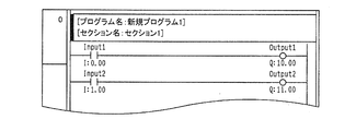
- FIG. 20 is a display screen showing an example of a ladder diagram created by the control program development support apparatus 10.
- FIG. 21 is a display screen showing an example of the unit configuration information screen.
- the control program development support apparatus 10 displays a basic screen as shown in FIG. 19 when a control program (for example, a ladder diagram in a ladder language) is created by a user program creation function (source code editor).
- a control program for example, a ladder diagram in a ladder language
- source code editor a user program creation function
- a screen for creating a control program is displayed in the right window W1
- a project selection screen W2 for project information relating to the unit configuration to be registered is displayed in the left window.
- the user creates a control program in the right window W1 using the source code editor (see FIG. 20).
- control program development support apparatus 10 displays the unit configuration information screen shown in FIG.
- control program development support device 10 is configured in advance to be compatible with a system that connects up to eight racks including “CPU rack 00”. , “Rack 01”, “rack 02”, “rack 03”,..., “Rack 07” are displayed in a tree shape as shown in FIG. 21, and the unit configuration of each rack is not displayed and is closed. Is displayed.
- the control program development support device 10 performs registration processing for the CPU unit 22 of “CPU rack 00”. That is, the control program development support apparatus 10 displays a screen prompting the user whether or not to newly register the unit configuration on the dialog window screen. Then, the control program development support apparatus 10 receives an input for registration by a user operation, and then displays a screen (not shown) for selecting the type and model of the CPU unit 22 in the PLC 200, and selects the input. Prompt.
- control program development support device 10 receives the input of the type and type information of the CPU unit 22 by a user operation. For example, when the user selects the CPU unit 22 of the type “CJ2H-CPU68-EIP”, the control program development support apparatus 10 registers the type of the target CPU unit 22 and the initial information of the unit configuration of the CPU rack. . The model of the CPU unit 22 registered in this way is displayed at the top of the tree display of the unit configuration information screen in FIG.
- control program development support device 10 registers the units (high function I / O unit, basic I / O unit) on the unit configuration information screen.
- FIG. 22 is a display screen showing a state in which the rack item is opened on the unit configuration information screen shown in FIG.
- FIG. 22 shows a state in which “CPU rack 00” is opened.
- each rack item is configured so that a maximum of 10 units (for the CPU rack, 10 units excluding the CPU unit) can be registered.
- no CPU units 22 other than “CPU rack 00” are registered in the control program development support apparatus 10, and thus the tree display of each unit for 10 units is displayed as “empty slot”. That is, a unit to be installed in a slot prepared in “CPU rack 00” (base unit) is not set.
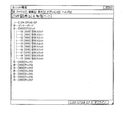
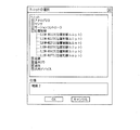
- FIG. 23 is an explanatory diagram of a screen showing an example of the unit list.
- the user When the unit is newly registered, the user operates the pointing device 12b (FIG. 18), selects the “free slot” field in the tree display shown in FIG. 22, and double-clicks the unit shown in FIG.
- the selection screen is displayed in a separate window.
- the control program development support apparatus 10 displays a unit selection screen with reference to a unit information storage unit (not shown) that stores unit information related to the unit.
- the unit information related to the unit stored in the unit information storage unit is specified by, for example, a list of types of units, a list of models, functions for each unit, parameters to be set, and each model. Channel information about each unit and information for specifying the memory capacity.
- the unit selection screen shown in FIG. 23 displays the target units constituting the PLC 200 in a tree structure for each type. For example, various units such as “analog I / O unit”, “sensor unit”, “motion controller”, “position control unit”, “temperature adjustment unit”, “basic I / O unit”, “communication unit” Is displayed.
- control program development support apparatus 10 When the control program development support apparatus 10 detects that the user clicks on the pointing device 12b with “+” on the tree display screen, the control program development support apparatus 10 displays the unit type information obtained by referring to the unit information storage unit. In the screen displayed in this way, the user searches for a unit to be used from the unit list, selects it, and registers it (“CJW-NC213” in the example shown).
- FIG. 24 is a display screen showing the unit configuration screen after executing the unit registration operation.
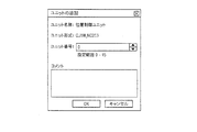
- FIG. 25 is a display screen showing an example of a unit addition screen.
- the control program development support apparatus 10 reads and displays the “model” information stored in the unit information storage unit. The specific name indicated by () after the model is displayed in the “model” column of the unit information storage unit.
- control program development support apparatus 10 displays the unit addition screen shown in FIG. And register the unit number.
- the control program development support device 10 searches the table for the model information definition file of the target unit, and acquires the number of occupied channels, the number of input channels, and the number of output channels from the model information definition file.
- the control program development support apparatus 10 acquires necessary information by reading the model information definition file for the corresponding unit.
- the control program development support apparatus 10 obtains necessary information from the number of occupied channels and the input / output type.
- control program development support apparatus 10 calculates the head address from the unit number of the unit, and assigns it to the high-function unit from the number of occupied channels, the number of input channels, and the number of output channels. Calculate the input port address and output port address. The calculation of the input / output address is performed as follows.
- a memory area from the memory address “0000” channel of the memory M of the CPU unit 22 is prepared in the high-function unit, and a memory area of 10 channels is secured per unit (one occupied channel).
- the start address of the memory area used for the high-function unit in the memory M of the CPU unit is “0000” channel. Up to 0009 "channel is reserved.
- the start address of the high-function unit of the memory M of the CPU unit is “0010” channel, and the memory addresses from “0010” channel to “0019” channel are reserved. Is done.
- the start address of the memory area allocated to the high-functional unit with the unit number N can be obtained by a simple expression such as “00 + 10 ⁇ N” channel. Further, the final address of the memory area allocated to the unit can be obtained based on the number of occupied channels.
- the memory automatic allocation of the memory addresses of the input channel and the output channel by the control program development support apparatus 10 is performed according to the following rules. That is, the slot arrangement position of each unit is uniquely determined by the rack number and the slot number. Therefore, the rack numbers (the rack number of “CPU rack 00” is “00”) are sorted in ascending order, and in the case of the same rack number, the slot numbers are sorted in ascending order, and the memory of the CPU unit 22 starts from the first unit. Allocation of M memory addresses is performed.
- the memory M to be allocated is configured to be continuously allocated unlike the case of the high-function unit.
- the control program development support apparatus 10 can create a unit input / output table TB as shown in FIG. 26 described later by performing the memory address assignment operation described above.
- the input / output table TB is temporarily stored, for example, in a volatile memory (not shown) such as a RAM in the control program development support apparatus 10, or stored in a non-volatile memory (not shown) such as a hard disk. Is done.
- FIG. 26 is a schematic diagram showing an example of the data structure of the input / output table TB stored in the control program development support apparatus 10.
- control program development support device 10 uses the “00” bit, “01” bit, “02” of the memory address “0000” channel of the memory M for the input unit 31 arranged in the slot 0 of “Rack 00”. By assigning bits,..., It is possible to correspond to “input port 00”, “input port 01”, “input port 02”,.
- the control program development support apparatus 10 assigns the “00” bit, “01” bit, “02” bit,... Of the memory address “0001” channel of the memory M, thereby “input port 10”, “input port 11”. , “Input port 12”,.
- control program development support device 10 sets the “00” bit, “01” bit, “02” bit of the memory address “0010” channel of the memory M for the output unit 32 arranged in the slot 1 of “Rack 00”. ,... Can be made to correspond to “output port 00”, “output port 01”, “output port 02”,... (See FIG. 18).
- the control program development support apparatus 10 assigns the “00” bit, “01” bit, “02” bit,... Of the memory address “0011” channel of the memory M, thereby “output port 10”, “output port 11”. , “Output port 12”,.
- control program development support device 10 assigns the memory address of the memory M. It can be carried out. The same applies to “Rack 02” and thereafter.
- the memory address (address value of the memory M) is added to the symbol / contact in FIG. ).
- FIG. 27 is a display screen showing various data such as addresses for variables. As shown in FIG. 27, the user sets a variable indicating the type of the port in association with the memory address so that it can be understood what type of port of which unit is allocated to the allocated memory address. Sometimes set. 20 and 27, “XX” in the memory address (XX.YY) represents a channel, and “YY” represents a bit in the “XX” channel. In FIG. 20, “I” shown before the memory address (XX.YY) represents an input area memory address, and “Q” represents an output area memory address.
- the user describes (inputs) the “00” bit memory address (0.00) of the “0000” channel for the variable “Input1” indicating the type of the input port, and indicates the type of the output port.
- the memory address (10.00) of the “00” bit of the “0010” channel for the variable “Output1” (see FIG. 20)
- a ladder diagram in which the output port (contact point) of the variable “Output1” is turned on is created.
- the user inputs the “00” bit memory address (1.00) of the “0001” channel for the variable “Input2”, and the “00” bit memory address (11 of the “0011” channel for the variable “Output2”. .00) (see FIG. 20), a ladder diagram is created in which when the input port (contact point) of the variable “Input2” is turned on, the output port (contact point) of the variable “Output2” is turned on.
- the PLC 200 when various units are installed by the user according to the unit configuration allocated by the control program development support apparatus 10, the PLC 200 assigns a specific memory address, and various types of memory are allocated to the memory M of the CPU unit 22. An area for the unit is secured in advance. In other words, the allocation of the memory addresses of the various units actually arranged in the PLC 200 and the allocation of the memory addresses of the various units configured in the control program development support apparatus 10 are the same.
- the control program development support apparatus 10 converts the control program into an object code that can be executed by the CPU unit 22 using the memory address described in the control program, and downloads the object code to the PLC 200.
- the PLC 200 executes the object code sent from the control program development support apparatus 10 by the CPU unit 22.
- the unit configuration is not changed once various units are arranged, and may be changed (specifically, the unit is moved, changed, added or deleted) as necessary. .
- the PLC 200 executes the memory addresses assigned to the memory M of the CPU unit 22.
- the memory address described in the control program, and the variables such as “Input1” and “Output1” set corresponding to the memory address are different. As a result, the memory address described in the control program and the variable And inconvenience that the association with the port becomes meaningless.
- a control program development support device for creating a unit configuration for arranging a plurality of units connected to a CPU unit of a programmable controller in a plurality of slots in a rack, even if the unit configuration is modified
- a control program development support apparatus, a control program development support program, and a recording medium that do not need to perform operations such as changing a memory address in the control program and can thereby improve convenience associated with the modification of the unit configuration Is needed.
- This application discloses the following control program development support apparatus, control program development support program, and recording medium in order to solve the above-described problems.
- a control program development support device that creates a unit configuration for arranging a plurality of units connected to a CPU unit of a programmable controller in a plurality of slots in a rack.
- the control program development support device is configured to allocate a memory address of a memory in the CPU unit corresponding to a plurality of port IDs uniquely determined for a plurality of ports in the plurality of units.
- a memory allocation unit configured to create a correspondence table between memory addresses associated with the plurality of port IDs and the plurality of port IDs, and the plurality of ports
- a variable table creation unit configured to create a variable table indicating a correspondence relationship between a variable associated with an ID and the plurality of port IDs, and obtaining a port ID corresponding to the variable from the variable table
- the memory address corresponding to the acquired port ID in the address table And a configured address acquiring unit so as to al acquired.
- the address table creation unit is configured to rewrite the port ID in the unit before the change to the port ID in the unit after the change with respect to the address table.
- control program development support program includes a control unit in a control program development support device for creating a unit configuration for arranging a plurality of units connected to a CPU unit of a programmable controller in a plurality of slots in a rack.
- a step of allocating memory addresses of the memory in the CPU unit corresponding to a plurality of port IDs uniquely determined for a plurality of ports in the plurality of units, and a correspondence associated with the plurality of port IDs Creating an address table indicating the correspondence between the memory addresses and the plurality of port IDs, and creating a variable table indicating the correspondence between the variables associated with the plurality of port IDs and the plurality of port IDs
- the step Acquires the port ID corresponding to the number from the variable table, the memory address corresponding to the obtained port ID and a step of acquiring from the address table.
- the step of creating the address table includes the step of rewriting the port ID in the unit before the change to the port ID in the unit after the change with respect to the address table.
- the “ID” in the present disclosure is an abbreviation of “identification” and means an identification code.
- the rack may be a single rack or a plurality of racks.
- the port ID in the unit before the change is rewritten to the port ID in the unit after the change with respect to the address table.
- the port ID corresponding to the variable is acquired from the variable table.
- the memory address corresponding to the acquired port ID is acquired from the address table.
- a rack path name corresponding to the rack a slot path name corresponding to any one of the plurality of slots, and corresponding to any one slot
- a path format that hierarchically represents a channel path name corresponding to any one channel among a plurality of channels and a bit path name corresponding to any one bit among a plurality of bits for the one channel.
- a path is set in the path format in which the rack path name, the slot path name, the channel path name, and the bit path name are sequentially represented in a hierarchical manner on the display screen. Is displayed. Therefore, the user can easily recognize the arrangement positions of the plurality of units by the path.
- variable information receiving unit configured to receive input information of the variable so that the user can input the information of the variable.
- variable is automatically set based on the variable information receiving unit configured to receive the input information of the variable and the hierarchical physical configuration of the plurality of ports.
- variable information automatic setting part constituted as mentioned above is illustrated.
- the user determines whether to input the variable input information in the variable information receiving unit or whether to automatically set the variable in the variable information automatic setting unit as necessary. It can be used properly.
- a unit configuration diagram is created by arranging at least one unit of the plurality of units one by one in any one of the plurality of slots in the rack so that the position can be changed,
- a unit configuration diagram creation unit configured to detect which unit of the plurality of units has moved to which slot when the arrangement position of any one of the plurality of units is changed.
- the address table creation unit includes a change detected by the unit configuration diagram creation unit for the port ID in the unit before the change detected by the unit configuration diagram creation unit with respect to the address table. An example of rewriting the port ID in a later unit is illustrated.
- the unit configuration diagram when the unit configuration diagram is created, it is possible to detect which unit of the plurality of units has moved to which slot. It is possible to efficiently detect a change in the arrangement position of one unit.
- Another embodiment includes a unit information storage unit configured to store illustration information in which the rack and the plurality of units are illustrated in association with unit information regarding the plurality of units.
- the unit configuration diagram creation unit displays an illustration corresponding to the illustration information of the rack stored in the unit information storage unit on a display screen, and the plurality of units corresponding to the illustration information stored in the unit information storage unit At least one illustration of each unit is placed one by one so that it can be moved and displayed on the display screen by dragging and dropping to any one of the slots in the rack. Is configured to do.
- the “illustration (abbreviation of illustration)” here is a concept including illustration images such as figures, pictures, and photographs.
- At least one illustration of the plurality of units corresponding to the illustration information stored in the unit information storage unit is one by one for one illustration of the plurality of slots in the rack. Drag and drop to create a unit configuration diagram that can be moved and displayed on the display screen, so that the unit configuration in the unit configuration diagram can be visually modified by an illustration, and the unit configuration can be modified. It becomes possible to facilitate the work.
- the port ID in the unit before the change is rewritten to the port ID in the unit after the change in the address table, and the port ID corresponding to the variable is set in the variable table.
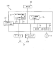
- FIG. 2 is a system configuration diagram schematically showing a control program development support device and a PLC that is set by the control program development support device.
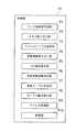
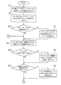
- FIG. 2 is a system configuration diagram schematically showing an internal structure of the control program development support device shown in FIG. 1. It is a system block diagram which shows roughly the control part in the control program development assistance apparatus shown in FIG. It is the flowchart of the first half part which shows an example of the allocation process which performs the allocation operation
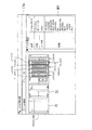
- FIG. 10 is a display screen for displaying “CPU rack 00” and a unit configuration diagram illustrating the units arranged in “CPU rack 00” with illustrations. It is screen explanatory drawing which shows an example of a unit list. It is a display screen which shows the state after modifying a unit structure from the unit structure figure shown in FIG. It is a schematic diagram which shows an example of the data structure of the address table which stores an address with respect to port ID in the unit comprised by the unit block diagram shown in FIG. It is the display screen which displayed the unit block diagram shown in FIG. 7 hierarchically.
- PLC programmable controller
- It is a schematic block diagram of the programmable controller (PLC) which shows an example of the system configuration which connects a CPU unit and various units. It is a display screen which shows the basic screen of a control program development support apparatus. It is a display screen which shows an example of the ladder diagram created with the control program development assistance apparatus. It is a display screen which shows an example of a unit structure information screen. It is a display screen which shows the state which opened the rack item with respect to the unit structure information screen shown in FIG. It is screen explanatory drawing which shows an example of a unit list. It is a display screen which shows the unit composition screen after performing unit registration operation. It is a display screen which shows an example of the unit addition screen. It is a schematic diagram which shows an example of the data structure of the input / output table stored in a control program development support apparatus. It is a display screen which shows various data, such as a memory address with respect to a variable.
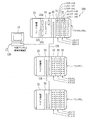
- FIG. 1 is a system configuration diagram schematically showing a control program development support apparatus 100 and a PLC 200 that is a setting target of the control program development support apparatus 100.
- the programmable controller (hereinafter referred to as PLC) 200 has the same configuration as the PLC 20 shown in FIG. In FIG. 1, the same members as those shown in FIG.
- the PLC 200 includes “CPU rack 00” and expansion racks (“rack 01”, “rack 02”,).
- CPU rack 00 and expansion racks (“rack 01”, “rack 02”, etc. Each include a power supply unit 21. Units arranged in one rack receive power supply from the power supply unit 21 connected to the rack.
- CPU rack 00 includes a CPU unit 22.
- the expansion racks (“Rack 01”, “Rack 02”,%) Do not include a CPU unit, and are managed (IO refresh or the like) by the CPU unit 22 in the “CPU rack 00”.
- the I / O control unit 40 is arranged.
- the I / O interface unit 50 is arranged in the expansion racks (“Rack 01”, “Rack 02”,).
- the “CPU rack 00” and the expansion rack (“rack 01”) are connected to each other by the I / O control unit 40 and the I / O interface unit 50 via the wiring cable CB.
- the expansion racks (“Rack 01”, “Rack 02”,...) Are connected to each other by the I / O interface unit 50 via the wiring cable CB.
- the “CPU rack 00” and the expansion racks (“rack 01”, “rack 02”,...) Can cooperate with each other so that they can communicate with each other.
- the PLC 200 is constructed by connecting three racks.
- the number of racks for constructing the PLC 200 is arbitrary, and there may be one rack (only “CPU rack 00”). That is, the number of expansion racks may be one. Further, only the “CPU rack 00” may be used without providing an expansion rack. Further, the power supply units 21 mounted in the “CPU rack 00” and the expansion racks (“rack 01”, “rack 02”,...) May be of the same type or different types.
- the “CPU rack 00” has an input unit 31 arranged in slot 0 and an output unit 32 arranged in slot 1. . Also, in “Rack 01”, among the slot 0, slot 1,..., The CPU high function unit 33 is arranged in the slot 0, the input unit 34 is arranged in the slot 1, and the output unit 35 is arranged in the slot 2. ing.
- the input units 31 and 34 have “input port 00”, “input port 01”, “input port 02” corresponding to contacts (for example, 8 points, 16 points, 32 points, 64 points, etc.) such as sensors and switches. , ... are provided.
- the output units 32 and 35 include “output port 00”, “output port 01”, “output port 02”, which correspond to contacts (for example, 8 points, 16 points, 32 points, 64 points, etc.) such as actuators and relays. ... is provided.
- FIG. 2 is a system configuration diagram schematically showing the internal structure of the control program development support apparatus 100 shown in FIG.
- the control program development support apparatus 100 combines various units to construct a PLC 200 having an arbitrary configuration, or to construct a PLC system for obtaining an appropriate unit configuration when designing a PLC configuration that matches a control target. Provide support functions.
- the control program development support apparatus 100 having a PLC system construction support function is called a PLC system construction support apparatus or a configurator. Further, the control program development support device 100 has a function of creating a control program (user program) to be executed by the PLC 200.
- An example of the control program includes a ladder program represented by a ladder diagram.
- a device having a function of creating a control program is called a ladder editor, or a control program creation device, a control program editing device, a programming device, or the like.
- the control program development support apparatus 100 is configured by installing a predetermined application program for realizing a PLC system construction support function or a user program creation function in a personal computer.
- the control program development support apparatus 100 sets various parameters for a normal I / O unit and other units, and downloads the set setting information to each device (unit) via a network or the like. May also be included.
- the control program development support apparatus 100 includes an input unit 12 including a keyboard 12a, a pointing device 12b, and the like as an external device (man machine interface), and a display having a display screen 13a (see FIG. 1).
- the display unit 13 is provided.
- control program development support device 100 executes a control program development support program, executes various arithmetic processes, and creates various unit processes to create unit configuration information
- the CPU 14 an execution processing storage unit 15 that is appropriately used as a work memory when the control unit 14 executes various processes such as arithmetic processing, and a unit information storage unit 16 that stores information about the unit.
- a COM port 17 used when downloading information set in the various units constituting the PLC 200 and created in the control unit 14 to the PLC 200, and a reading unit 18.
- the execution processing storage unit 15 includes a volatile memory 15a such as a RAM and a nonvolatile memory 15b such as a hard disk device or a flash memory.
- a volatile memory 15a such as a RAM
- a nonvolatile memory 15b such as a hard disk device or a flash memory.
- the control program development read by the reading unit 18 that reads the recording medium R such as a CD (Compact Disc) -ROM (Read-Only Memory) in which a control program development support program BP described later is recorded.
- Software including the support program BP and file data of illustration information to be described later are stored (installed) in advance.
- the nonvolatile memory 15b is configured to store processing data such as an address table and a variable table described later.
- the recording medium R may be a USB (Universal Serial Bus) memory or an SD (Secure Digital) memory card.
- the control unit 14 displays various input screens on the display unit 13, and the user operates the input unit 12 to receive necessary information and determines unit configuration information.
- the unit information related to the unit stored in the unit information storage unit 16 is, for example, a list of types, types, etc., specifications such as manufacturer name, voltage, current, etc., functions for each unit, and setting targets.
- the parameters are channel information about the unit specified by each type, and information for specifying the memory capacity.
- the unit information storage unit 16 also stores illustration information as will be described later.
- the control unit 14 also provides memory addresses (hereinafter simply referred to as addresses) of the memory M in the CPU unit 22 for I / O data used by basic I / O units such as the input units 31 and 34 and the output units 32 and 35. Assigns.
- FIG. 3 is a system configuration diagram schematically showing the control unit 14 in the control program development support apparatus 100 shown in FIG.
- the control unit 14 includes a unit configuration diagram creation unit P1, a memory allocation unit P2, an address table registration unit P3, a variable information reception unit P4, a path setting display unit P5, a variable information automatic setting unit P6, and a variable table.
- the creation unit P7, the port ID rewriting unit P8, the address acquisition unit P9, and the conversion unit P10 are configured to function.
- the address table registration unit P3 and the port ID rewriting unit P8 constitute an address table creation unit according to the present embodiment.
- the control program development support program BP includes a unit configuration diagram creation step corresponding to the unit configuration diagram creation unit P1, a memory allocation step corresponding to the memory allocation unit P2, and an address table registration step corresponding to the address table registration unit P3.
- a variable information reception step corresponding to the variable information reception unit P4 a path setting display step corresponding to the path setting display unit P5, a variable information automatic setting step corresponding to the variable information automatic setting unit P6, and a variable table creation unit P7.
- the control unit includes a step including a variable table creation step corresponding to, a port ID rewrite step corresponding to the port ID rewrite unit P8, an address acquisition step corresponding to the address acquisition unit P9, and a conversion step corresponding to the conversion unit P10 14 is executed.
- FIG. 4 and FIG. 5 are flowcharts of the first half and the second half, respectively, showing an example of an allocation process for performing an address allocation operation of the memory M in the CPU unit 22 corresponding to a plurality of ports in a plurality of units.
- the plurality of ports are “input port 00”, “input port 01”, “input port 02”,... “Output port 00”, “output port”. .., “0”, “output port 02”,..., And units arranged in slot 0, slot 1,. “Input port 02”,..., “Output port 01”, “output port 02”,.
- the unit configuration diagram creation step S1 shown in FIG. 4 is a unit configuration diagram in which at least one of unit 0, unit 1,... Is arranged in one of a plurality of slots in the rack in such a manner that its position can be changed.
- any unit of unit 0, unit 1 For detecting which slot has moved to which slot.
- the control unit 14 displays an illustration of “CPU rack 00” on the display screen 13a (see FIG. 1) of the display unit 13, and further displays the unit illustration in a movable manner. Create a unit configuration diagram.
- FIG. 6 is a schematic configuration diagram illustrating an example of a partial data structure of unit information in the unit information storage unit 16.
- FIG. 7 is a display screen for displaying “CPU rack 00” and a unit configuration diagram showing the units arranged in “CPU rack 00” in illustration.
- illustration information IL that illustrates a plurality of units 0, units 1,. ,... Are stored in advance in association with the types TY and names TN.
- the illustration information IL is the name of file data.
- the control unit 14 reads out the file data stored in the nonvolatile memory 15b of the execution processing storage unit 15 (see FIG. 2) from the name of the file data, and selects the unit selected from the units 0, 1 and so on. It is configured to be illustrated.
- the unit information storage unit 16 also stores illustration information IL of “CPU rack 00”, “rack 01”, “rack 02”,.
- the control unit 14 reads the illustration information IL corresponding to “CPU rack 00” from the unit information storage unit 16, and “CPU rack 00” based on the read illustration information IL. Is displayed on the display screen 13 a of the display unit 13.
- FIG. 8 is an explanatory diagram of a screen showing an example of the unit list.
- the user operates the pointing device 12b (see FIG. 1) to select any slot (for example, slot 3) in the illustration of “CPU rack 00” by double-clicking or the like. Is displayed in a separate window. That is, when the control unit 14 detects that the user has clicked the pointing device 12b at the slot position of the “CPU rack 00” (for example, slot 3), the control unit 14 is obtained with reference to the unit information storage unit 16.
- the unit type information is displayed on the unit selection screen (see FIG. 8). Since the unit selection screen is the same as the unit selection screen shown in FIG. 23, detailed description will not be repeated.
- the tree display is expanded. That is, when the control unit 14 detects that the user has clicked the pointing device 12b in “+” on the tree display screen, the unit information obtained by referring to the unit information storage unit 16 is shown in FIG. Display on the unit selection screen.
- the user searches for a unit to be used from the unit list, and operates the pointing device 12b to select the unit to be used. That is, when the control unit 14 detects that the user has clicked the pointing device 12b at the position of the selected unit (for example, CJ1W-OD202) on the unit selection screen, the control unit 14 refers to the unit information storage unit 16.
- the illustration information IL of the obtained unit is illustrated and displayed in the slot position (for example, slot 3) of “CPU rack 00” in the unit configuration diagram shown in FIG.
- unit information such as model, name, and specification is displayed on the unit information screen W3 on the right side of the unit configuration diagram in FIG.
- control unit 14 displays any one of the units 0, 1, 1,... On the display unit 13 for any one of the slots 0, 1, 2,. Is arranged on the display screen 13a to create a unit configuration diagram.
- control unit 14 can modify the unit configuration by performing the following unit addition, movement, and deletion operations.
- FIG. 9 is a display screen showing a state after the unit configuration is modified from the unit configuration diagram shown in FIG.
- the user operates the pointing device 12b to select an illustration of the unit, and drags and drags the illustration of the selected unit (for example, unit 0 in slot 0). Move to another slot (for example, slot 1) by dropping. That is, when the control unit 14 detects that the user has dragged the pointing device 12b at the position of the selected unit (for example, unit 0 of slot 0) on the unit selection screen, the control unit 14 moves the selected unit with the cursor. Let When the control unit 14 detects that the user has dropped the pointing device 12b at the position of another slot (for example, slot 1), the control unit 14 moves the selected unit (for example, unit 0 in slot 0) to the other slot.
- another slot for example, slot 1
- the control unit 14 moves the unit (for example, unit 1) in the other slot (for example, slot 1) to the slot (for example, slot 0) of the selected unit.
- the control unit 14 also displays the position information of the unit to be moved (see the unit information screen W3 in FIG. 9 and the position information screen W4 on the lower right of the unit configuration diagram).
- the position information of the unit to be moved see the unit information screen W3 in FIG. 9 and the position information screen W4 on the lower right of the unit configuration diagram.
- the control unit 14 when displaying positional information, the content of the unit information on the unit information screen W3 displayed on the positional information screen W4 is simplified and displayed.
- the control unit 14 when the control unit 14 moves the selected unit (for example, unit 0) across one or a plurality of slots (for example, slot 1), the control unit 14 (for example, slot 2) has a unit (for example, slot 2).
- Unit 2 may be replaced with a selected unit (eg, unit 0).
- the control unit 14 moves to the slot (for example, slot 1) of the slot (for example, slot 1) next to the slot (for example, slot 0) next to the selected unit (for example, slot 0).
- the unit (1) is moved, and the unit (for example, unit 2) in the slot (for example, slot 2) next to the slot (for example, slot 2 in FIG. 7) is moved to the slot of the moved unit (for example, slot 1 of unit 1). Good.
- control unit 14 displays at least one illustration of unit 0, unit 1,... (For example, unit 0) one by one of the slots 0, 1, 2,.
- a unit configuration diagram is created by arranging two illustrations so that they can be moved and displayed on the display screen 13a of the display unit 13 in accordance with a drag-and-drop operation (see FIG. 9).
- the user operates the pointing device 12b to select a unit illustration, and deletes (deletes) the illustration of the selected unit (for example, the unit in slot 3) by a deletion operation. That is, when the control unit 14 detects that the user has clicked the pointing device 12b at the position of the selected unit (for example, the unit in the slot 3) on the unit selection screen, the selected unit is selectively displayed ( For example, when the user presses a predetermined key (for example, delete [delete] key) on the keyboard 12a (see FIG. 1), the slit in which the selected unit (for example, the unit in slot 3) is placed is received. Delete (erase) from (for example, slit 3).
- a predetermined key for example, delete [delete] key
- a slot position (slot number) corresponding to position information on the screen is stored in association with each other.
- the control unit 14 can detect (recognize) that the unit configuration has been modified, and further, which illustration of the unit 0, unit 1,... Has moved to which slot.
- the control unit 14 is configured to set a plurality of port IDs to be identifiable for a plurality of ports, respectively. Thereby, a plurality of port IDs are uniquely determined for a plurality of ports.
- step S31 shown in FIG. 4 the control unit 14 determines whether or not an address table TB1 shown in FIG. 10 to be described later is newly registered, that is, whether or not data is registered in the address table TB1.
- step S31: Yes the control unit 14 shifts the control to the address table registration step S3.
- step S31: No the control unit 14 proceeds to variable information reception step S4.
- the control unit 14 is associated with a plurality of port IDs uniquely determined for the ports Pt in the unit 0, unit 1,.
- An address table TB1 indicating the correspondence between addresses and a plurality of port IDs is registered.
- the address table TB1 is configured to be stored in the nonvolatile memory 15b of the execution process storage unit 15.
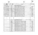
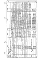
- FIG. 10 is a schematic diagram showing an example of the data structure of the address table TB1 for storing addresses for the port IDs in the units configured in the unit configuration diagram shown in FIG.
- the control unit 14 sets “input port 00”, “input port 01”, “input port 02”,... For the input unit 0 (model CJ1W-ID 201) arranged in slot 0 of “rack 00”. Corresponding to the port IDs “0000”, “0001”, “0002”,..., “00” bit, “01” bit, “02” bit,. The control unit 14 corresponds to the port IDs “0100”, “0101”, “0102”,... Of “input port 10”, “input port 11”, “input port 12”,. “00” bit, “01” bit, “02” bit,... The control unit 14 also sets the port IDs of “output port 00”, “output port 01”, “output port 02”,...
- the output unit 1 (model CJ1W-OC201) arranged in the slot 1 of “rack 00”. Corresponding to “1000”, “1001”, “1002”,..., The “00” bit, “01” bit, “02” bit,.
- the control unit 14 corresponds to “output port 10”, “output port 11”, “output port 12”,..., “00” bit, “01” bit, “02” of the address “0011” channel of the memory M. Assign bits, ...
- the value of the port ID is a value that does not change with respect to the unit even if the unit configuration is modified.
- variable information receiving step S4 Next, in the variable information receiving step S4 shown in FIG. 4, the control unit 14 receives input information of the variable Var associated with the port ID by an input operation using the keyboard 21a (see FIG. 1).
- control unit 14 hierarchically displays the units configured in the unit configuration diagram shown in FIG. 11 described later.
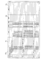
- FIG. 11 is a display screen in which the unit configuration diagram shown in FIG. 7 is hierarchically displayed.
- the symbol “R” means reading
- the symbol “W” means writing
- the symbol “RW” means both reading and writing. .
- the port Pt of the input unit 0 (model CJ1W-ID 201) realizes a hierarchical physical configuration such as a rack hierarchy, a unit hierarchy, and a port hierarchy.
- the rack hierarchy is represented by “CPU Rack 0”
- the unit hierarchy is represented by “CJ1W-ID201 (DC input unit)”
- the port hierarchy is represented by “Ch1_In”.
- the port Pt of the output unit 1 (model CJ1W-OC201) is expressed as “CPU Rack 0” in the rack hierarchy, “CJ1W-OC201 (relay contact output unit)” in the rack hierarchy, and “Ch1_Out” in the port hierarchy.
- control unit 14 is configured to accept comment information Co corresponding to the variable Var by an input operation using the keyboard 21a.
- the control part 14 implements path
- the path setting display step S5 as shown in FIG. 12, which will be described later, the path Pa is displayed in a path format in which the rack path name, slot path name, channel path name, and bit path name are represented hierarchically in order with respect to the port ID. 13 display screens 13a.
- FIG. 12 is a display screen that displays the port IDs in a hierarchical format that represents the port IDs.
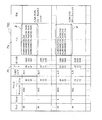
- FIG. 13 is a schematic diagram illustrating an example of a data structure in which a path name is added to the address table TB1 illustrated in FIG.
- the rack path name in FIG. 12 corresponding to “CPU rack 00” in FIG. 13 is “rack # 0” and in slot 0 in FIG.
- the corresponding slot path name in FIG. 12 corresponds to “slot # 0”
- the channel path name in FIG. 12 corresponding to channel “0000” in FIG. 13 corresponds to “Ch1_In”
- the figure corresponds to bit “xxx” in FIG. Twelve bit path names are set to “Ch_Inxx”, respectively.
- the rack path name in FIG. 12 corresponding to “CPU rack 00” in FIG. 13 is “rack # 0” and FIG.
- the control unit 14 determines, for the port ID, the rack path name corresponding to “CPU rack 00”, the slot path corresponding to any one of slot 0, slot 1, slot 2,. Name, a channel path name corresponding to any one channel among a plurality of channels for any one slot, and a bit path name corresponding to any one bit among a plurality of bits for any one channel in order
- the path Pa is set in the path format shown in the figure, and the path Pa is displayed on the display screen 13 a of the display unit 13. Note that a configuration in which the path Pa is always displayed may be used even if the user does not operate an icon (not shown) that instructs to display the port ID in the path format.
- variable information automatic setting step S6 the control part 14 implements variable information automatic setting step S6 shown in FIG. Specifically, in determination step S61, the control unit 14 determines whether or not to automatically set the variable Var. That is, when the control unit 14 detects that the user has clicked the pointing device 12b on an icon (not shown) that instructs automatic setting of the variable Var (determination step S61: Yes), the variable information automatic In the setting step S6, the control unit 14 automatically sets the variable Var extracted from the name of the hierarchical physical configuration of the port and displays it on the display screen 13a of the display unit 13 as shown in FIGS. To do.
- FIG. 14 is a display screen that displays the variable Var extracted and automatically set from the name of the hierarchical physical configuration of the port.
- variable Var of the input unit 0 (model CJ1W-ID201) has a device name “J01” in which the first three digits are attached to the unit “CJ1W-ID201” in the unit layer (see the position information screen W4 in FIG. 9).
- the middle three digits are “Ch1” acquired from at least two characters of “Ch1_In” in the port hierarchy, and the last two digits or four digits are the serial numbers for “Ch1_In” in the port hierarchy. .
- control unit 14 returns to the variable information receiving step S4 when the user clicks the pointing device 12b to any one of the variables Var.
- the input information of the operated variable Var is received by an input operation using the keyboard 21a.
- the control unit 14 determines whether or not to determine the variable Var. That is, when the variable Var is not fixed in the determination step S62 (determination step S62: No), the control unit 14 performs a click operation of the pointing device 12b by the user with respect to an icon (not shown) for instructing the end of the process. Until it is detected (determination step S63: No), the control proceeds to variable information reception step S4, and variable input information reception processing is performed. On the other hand, when the control unit 14 detects that a click operation has been performed on the icon instructing the end of the process (determination step S63: Yes), the control unit 14 shifts the control to the determination step S82.
- variable table creation step S7 when the control unit 14 receives a click operation of the pointing device 12b by the user with respect to an icon (not shown) instructing determination of the variable Var in the determination step S62 (determination step S62: Yes), the variable table creation step S7. Migrate to
- variable table creation step S7 the control unit 14 creates a variable table TB2 (see FIG. 15 to be described later) indicating the correspondence between the variable Var and the port ID associated with the port ID.
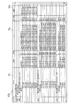
- FIG. 15 is a schematic diagram showing an example of the data structure of the variable table TB2 that stores the variable Var for the port ID for which the path Pa is set.
- the variable table TB2 is configured to be stored in the nonvolatile memory 15b of the execution process storage unit 15.
- variable names and data types are stored in association with port IDs and their path names.
- a path Pa of “rack # 0 / slot # 0 / Ch1_In” is stored for a byte-type (8-bit) variable Var (“J01_Ch1_In”).
- the control unit 14 performs the unit configuration diagram creation step S1 on the address table BT1 when the unit configurations of the units 0, 1 and so on are modified in the unit configuration diagram creation step S1.
- the port ID (specifically, the port ID for which the path Pa is set) in the unit before change (for example, unit 0, unit 1) detected in (1) is changed to the unit (after change) detected in the unit configuration diagram creation step S1. For example, it is rewritten to the port ID in unit 1, unit 0).
- FIG. 16 is a schematic diagram showing an example of the data structure after the unit configuration is modified in the address table TB1 shown in FIG.
- FIG. 17 is a display screen displayed after the unit configuration is modified on the display screen shown in FIG.
- unit 0 in slot 0 and unit 1 in slot 1 are interchanged with each other.
- the port ID “0000” stored in the “00” bit of the “0000” channel, the “01” bit of the “0000” channel, the “02” bit of the “0000” channel,.
- "0001” ("rack # 0 / slot # 0 / Ch1_In / Ch1_In01” in the path format)
- "0002” track # 0 / slot # 0 / Ch1_In / Ch1_In02 ”), as shown by ⁇ in FIG. 16,“ 00 ”bit of“ 0010 ”channel,“ 01 ”bit of“ 0010 ”channel,“ 0010 ”channel It is rewritten to the address of “02” bit,.
- "1001” rack # 0 / slot # 1 / Ch1_Out / Ch1_Out01” in the path format
- “1002” track # 0 / slot # 1 / Ch1_Out / Ch1_Out02 ”
- “ 00 ”bit of“ 0000 ”channel,“ 01 ”bit of“ 0000 ”channel,“ 0000 ”channel It is rewritten to the address of “02” bit,.
- the rack path name of FIG. 17 corresponding to “CPU rack 00” of FIG. 16 for the port Pt of the input unit 0 (model CJ1W-ID 201 in this example) 17 is “rack # 0”
- the slot path name in FIG. 17 corresponding to slot 1 in FIG. 16 is “slot # 1”
- the channel path name in FIG. 17 corresponding to channel “0010” in FIG. 16 is “Ch1_In”.
- the bit path name of FIG. 17 corresponding to the bit “xx” of FIG. 16 is set to “Ch_Inxx”.
- FIG. 17 corresponding to “CPU rack 00” in FIG. 16 corresponds to “rack # 0” and corresponds to slot 0 in FIG.
- the slot path name in FIG. 17 corresponds to “slot # 0”
- the channel path name in FIG. 17 corresponding to the channel “0000” in FIG. 16 corresponds to “Ch1_Out”
- FIG. 17 corresponds to the bit “xxx” in FIG. Is set to “Ch_Outxx”.
- “XX” represents a value corresponding to a bit of the address.
- the port ID rewriting step S8 may always be processed. .
- variable table TB2 shown in FIG. 15, if the arrangement position of any one of the units 0, 1, 1,... The settings are configured to be updated.
- control unit 14 determines whether or not to convert the control program into an object code. That is, when the control unit 14 detects that the user has clicked on the pointing device 12b with respect to an icon (not shown) that instructs conversion to an object code of the control program (determination step S82: Yes). Control proceeds to address acquisition step S9.
- the control unit 14 acquires the port ID corresponding to the variable Var described in the control program from the variable table TB2 (see FIG. 15), and the address corresponding to the acquired port ID is updated with data. Obtained from the address table TB1 (see FIG. 16).
- the port ID “0000” (“rack # 0 / slot # 0 / Ch1_In / Ch1_In00” in the path format) corresponding to the variable Var (“J01_Ch1_In00”) of the variable table TB2 shown in FIG. 15 before the unit configuration is modified.
- the address corresponding to “0000” (“rack # 0 / slot # 1 / Ch1_In / Ch1_In00” in the path format) is the bit “00” of the channel “0010”.
- the path Pa set to the port ID “0000” corresponding to the variable Var (“J01_Ch1_In00”) of the variable table TB2 illustrated in FIG. 15 is “rack # 0 / slot #” as illustrated in FIGS. Since it is updated to “1 / Ch1_In / Ch1_In00”, the user can refer to the latest path Pa.
- control unit 14 converts (specifically, compiles) the control program into an object code that can be executed by the CPU unit 22, using the acquired address.
- the control unit 14 determines the port ID in the unit before the change with respect to the address table TB1.
- the port ID corresponding to the variable Var is acquired from the variable table TB2
- the address corresponding to the acquired port ID is acquired from the address table TB1.
- control unit 14 sets the path Pa in a path format in which the rack path name, the slot path name, the channel path name, and the bit path name are hierarchically represented for the port ID. Since the information is displayed, the user can easily recognize the unit arrangement position simply by looking at the path Pa.
- variable information receiving step S4 since the control unit 14 performs the variable information receiving step S4 and the variable information automatic setting step S6, the variable information receiving step S4 inputs the input information of the variable Var, or The user can select whether the variable Var is automatically set in the variable information automatic setting step S6 as necessary.
- the unit configuration diagram may be a tree-type structure diagram as shown in FIG.
- a unit configuration diagram is created by arranging a unit illustration so that it can be moved and displayed on the display screen 13a of the display unit 13 by dragging and dropping the slot illustration. Therefore, the unit configuration in the unit configuration diagram can be visually modified by an illustration, and the unit configuration modification work can be facilitated.
- a plurality of PLCs 200 may be provided, and a plurality of PLCs 200 may be connected to each other via a network such as a LAN.
- a display form of the path Pa set in the port ID a display form in which a network path name (for example, PLC name) is added to the head can be exemplified.
- Control program development support apparatus 200 PLC BP control program development support program M memory Pa path Pt port P1 unit configuration diagram creation unit P2 memory allocation unit P3 address table registration unit P4 variable information reception unit P5 path setting display unit P6 variable information automatic setting unit P7 variable table creation unit P8 Port ID rewrite unit P9 Address acquisition unit P10 Conversion unit R Recording medium TB1 Address table TB2 Variable table Var variable
Landscapes
- Physics & Mathematics (AREA)
- General Physics & Mathematics (AREA)
- Engineering & Computer Science (AREA)
- Automation & Control Theory (AREA)
- Programmable Controllers (AREA)
Abstract
たとえユニット構成が改変されたとしても、制御プログラムにおけるメモリアドレスの変更等の作業を行う必要がなく、これにより、ユニット構成の改変に伴う利便性を向上させることが可能な制御プログラム開発支援装置、制御プログラム開発支援用プログラム及び記録媒体を提供する。ポートIDに対応して関連付けられるメモリアドレスとポートIDとの対応関係を示すアドレステーブル(TB1)を作成し、ポートIDに対応して関連付けられる変数VarとポートIDとの対応関係を示す変数テーブル(TB2)を作成し、アドレステーブル(TB1)に対して、変更前のユニットにおけるポートIDを、変更後のユニットにおけるポートIDに書き換え、変数Varに対応するポートIDを変数テーブル(TB2)から取得し、取得したポートIDに対応するメモリアドレスをアドレステーブル(TB1)から取得する。
Description
本開示は、制御プログラム開発支援装置に関し、特に、プログラマブルコントローラのCPUユニットに接続される複数のユニットをラック内における複数のスロットにそれぞれ配置するためのユニット構成を作成する制御プログラム開発支援装置、制御プログラム開発支援用プログラム及び記録媒体に関する。
生産工場の製造現場などに設置されるFA(ファクトリーオートメーション)システムを制御するためのPLC(プログラマブルコントローラ)では、一般的に、制御プログラム(ユーザプログラム)に基づいて演算実行するCPU(Central Processing Unit)ユニットに対して、センサやスイッチなどの入力機器の接続を受けて当該入力機器のオン・オフ信号を入力信号として取り込む入力ユニット、アクチュエータやリレーなどの出力機器の接続を受けて当該出力機器に対して出力信号を送り出す出力ユニット、上位端末装置などと接続を確立して当該端末装置と情報をやりとりする通信ユニット、各ユニットに電源を供給する電源ユニットその他の各種ユニットが接続される。これらの各種ユニットがそれぞれ1段又は多段のラックに配置されてPLCが構成されている。
図18は、CPUユニット22と各種ユニット31,32,…とを接続するシステム構成の一例を示すプログラマブルコントローラ(PLC)200の概略構成図である。
PLC200は、電源ユニット21とCPUユニット22とを含む「CPUラック00」を備える。また、PLC200には、電源ユニット21を含む増設ラック(「ラック01」,「ラック02」,…)が増設されることもある。
「CPUラック00」には、電源ユニット21及びCPUユニット22に加えて、複数のユニット(基本入力ユニット、基本出力ユニット、高機能入力ユニット、高機能出力ユニットやCPU高機能ユニット等の構成ユニット)が配置される。また、ラックが増設される場合、「CPUラック00」には、さらにI/O(入出力)コントロールユニット40が配置され、「ラック01」,「ラック02」,…には、I/Oインターフェースユニット50、複数のユニット(基本入力ユニット、基本出力ユニット、高機能入力ユニット、高機能出力ユニットやCPU高機能ユニット等の構成ユニット)が配置される。I/Oコントロールユニット40とI/Oインターフェースユニット50とは、配線ケーブルCBを介して互いに接続される。
図18の例では、「CPUラック00」には、複数のスロット(スロット0,スロット1,…)のうち、スロット0に入力ユニット31が、スロット1に出力ユニット32が配置されている。また、「ラック01」には、スロット0,スロット1,…のうち、スロット0にCPU高機能ユニット33が、スロット1に入力ユニット34が、スロット2に出力ユニット35が配置されている。
また、入力ユニット31,34には、センサやスイッチ等の接点に相当する「入力ポート00」,「入力ポート01」,「入力ポート02」,…が設けられている。出力ユニット32,35には、アクチュエータやリレー等の接点に相当する「出力ポート00」,「出力ポート01」,「出力ポート02」,…が設けられている。
CPUユニット22は、制御プログラムを記憶するプログラムメモリ22aと、入力ユニット31,34が取り込んだ入力信号と制御プログラムの演算結果である出力信号とをそれぞれ記憶するデータメモリ22bと、制御プログラムに基づく演算処理等をする処理プロセッサ部22cとを備えている。PLC200は、プログラミングツール装置として作用する制御プログラム開発支援装置10の接続を受ける。PLC200は、制御プログラム開発支援装置10によって作成または編集され、さらに、CPUユニット22で実行可能なオブジェクトコードに変換された制御プログラムを実行する。
詳しくは、制御プログラムは、PLC200を稼働させる前に、ユーザが制御プログラム開発支援装置10を操作することにより、例えば、ラダー図(ラダーチャート)で表現されるラダー言語で記述されて作成される。
そして、作成された制御プログラムは、制御プログラム開発支援装置10によってラダー図のシンボルが命令語に変換され、CPUユニット22に応じたオペランドが規定され、CPUユニット22にダウンロードされる。
CPUユニット22の処理プロセッサ部22cは、プログラムメモリ22aから制御プログラムの命令語を順次読み出して、読み出した命令語のオペランドに従うI/Oメモリ等のメモリMのメモリアドレスに基づいてデータメモリ22bから入力信号のデータを読み出す。処理プロセッサ部22cは、読み出したデータを制御プログラムに従って論理演算し、演算結果をデータメモリ22bに記憶する。処理プロセッサ部22cは、記憶した演算結果を出力信号として出力ユニット32,35へ出力する。CPUユニット22の処理プロセッサ部22cは、入力信号の読み出し処理と、制御プログラムの実行処理と、出力処理の出力処理とをサイクリックに実行する。
制御プログラムが、例えば、ラダー言語のラダー図を用いて作成された場合、制御プログラム上で接点を表すシンボルの上に、制御プログラムを実行するCPUユニット22において使用するメモリMにおけるメモリアドレスが、併記される。接点は、例えば、CPUユニット22がI/Oデータ(I/Oポートの入力データ若しくは出力データ)として扱う対象を指し、具体的にはセンサやスイッチの接点をいう。シンボルは、ラダー言語で書かれた制御プログラム上で接点を示す表現記号である。例えば、入力接点のシンボルは「-││-」であり、出力接点のシンボルは「-○-」である(以下の説明では、ラダー図で書かれた制御プログラムにおけるシンボル又は接点を特に区別しない場合は、「シンボル・接点」ということもある)。メモリアドレスは、例えば、CPUユニット22がI/Oデータとして扱う場合、接点に対応する各I/Oポートをメモリ割り付けすることで決まる。メモリアドレスは、CPUユニット22が演算に使用する各I/Oデータが格納されるメモリMのアドレス番号を示す。
従来の制御プログラム開発支援装置10は、構成ユニット31,32,…におけるスロット0,スロット1,…の配置位置(スロット装着位置)によりメモリアドレスを決定する。具体的には、制御プログラム開発支援装置10は、スロット0,スロット1に配置(装着)された入力ユニット31,34における「入力ポート00」,「入力ポート01」,「入力ポート02」,…に対応してメモリMのメモリアドレスを割り付け、スロット1,スロット2に配置(装着)された出力ユニット32,35における「出力ポート00」,「出力ポート01」,「出力ポート02」,…に対応してメモリMのメモリアドレスを自動的に割り付けるように構成されている(特許文献1(特開2006-243841号公報)参照)。
以下に、構成ユニット31,32,…におけるスロット0,スロット1,…の配置位置によりメモリMのメモリアドレスを自動的に割り付ける手順について説明する。
図19は、制御プログラム開発支援装置10の基本画面を示す表示画面である。図20は、制御プログラム開発支援装置10で作成されたラダー図の一例を示す表示画面である。図21は、ユニット構成情報画面の一例を示す表示画面である。
制御プログラム開発支援装置10は、ユーザプログラム作成機能(ソースコードエディタ)で制御プログラム(例えば、ラダー言語によるラダー図)が作成されるとき、図19に示すような基本画面を表示する。基本画面では、右側のウインドウW1に制御プログラムを作成する画面が表示され、左側のウインドウにこれから登録するユニット構成に関するプロジェクト情報のプロジェクト選択画面W2が表示された状態となる。ユーザは、ソースコードエディタを用いて、右側のウインドウW1内に制御プログラムを作成する(図20参照)。
次に、図19に示す基本表示画面に対し、ユーザが、ポインティングデバイス12b(図18参照)を操作してプロジェクト選択画面W2中にツリー表示された「ユニット構成情報」をダブルクリック等により選択すると、制御プログラム開発支援装置10は、図21に示すユニット構成情報画面を表示する。
この例では、制御プログラム開発支援装置10は、予め、「CPUラック00」を含めて最大8個のラックを接続するシステムに対応できるように構成されているため、初期画面では、「CPUラック00」,「ラック01」,「ラック02」,「ラック03」,…,「ラック07」のみが図21のようにツリー状に表示され、各ラックのユニット構成が表示されずに閉じた状態で表示される。
なお、ユニット構成情報画面(図21参照)を表示する前には、制御プログラム開発支援装置10は、「CPUラック00」のCPUユニット22を登録処理する。つまり、制御プログラム開発支援装置10は、ユーザに対して、ユニット構成を新規登録するかどうかを促す画面をダイアログウインドウ画面にて表示する。そして、制御プログラム開発支援装置10は、ユーザ操作により登録する旨の入力を受信し、次に、PLC200におけるCPUユニット22の種別および型式を選択する画面(図示せず)を表示し、選択入力を促す。
具体的には、制御プログラム開発支援装置10は、ユーザ操作によりCPUユニット22の種別および型式情報の入力を受信する。例えば、ユーザが「CJ2H-CPU68-EIP」という型式のCPUユニット22を選択すると、制御プログラム開発支援装置10は、対象のCPUユニット22の種別と、CPUラックのユニット構成の初期情報とを登録する。こうして登録されたCPUユニット22の型式が、図21のユニット構成情報画面のツリー表示の最上段に表示される。
次いで、制御プログラム開発支援装置10は、ユニット構成情報画面にユニット(高機能I/Oユニット、基本I/Oユニット)を登録する。
図22は、図21に示すユニット構成情報画面に対してラック項目を開いた状態を示す表示画面である。
具体的には、設定しようとするラック項目が、初期画面等のように閉じている場合には、ユーザが、使用する(設定する)ラック項目のツリー表示の先頭に表示された[+]ボタンをクリックすると、制御プログラム開発支援装置10は、図22に示すように適宜のラック項目を開く。図22は、「CPUラック00」が開かれた状態を示している。図22の例では、各ラック項目には、最大で10台分のユニット(CPUラックについては、CPUユニットを除いて10台分のユニット)を登録することができるように構成されている。初期では「CPUラック00」のCPUユニット22以外は制御プログラム開発支援装置10に登録されていないから、10台分の各ユニットのツリー表示はすべて「空きスロット」と表示される。すなわち、「CPUラック00」(ベースユニット)に用意されたスロットに装着されるべきユニットは設定されていない。
次に、実際のユニットの登録処理を行う場合について説明する。図23は、ユニット一覧の一例を示す画面説明図である。
ユニットが新規登録の場合には、ユーザはポインティングデバイス12b(図18)を操作して、図22に示すツリー表示中の「空きスロット」の欄を選択し、ダブルクリックすると、図23に示すユニット選択画面が別ウインドウで表示される。
制御プログラム開発支援装置10は、ユニットに関するユニット情報を格納したユニット情報記憶部(図示しない)を参照して、ユニット選択画面を表示する。ユニット情報記憶部に格納されるユニットに関するユニット情報は、例えば、ユニットの種類と、型式等の一覧リストと、各ユニットについての機能と、設定対象となるパラメータと、さらには、各型式で特定されるユニットについてのチャネル情報と、それぞれがメモリ容量を特定するための情報とを含む。
図23に示すユニット選択画面は、PLC200を構成する対象ユニットを種別ごとにツリー構造で表示する。例えば「アナログI/Oユニット」、「センサユニット」、「モーションコントローラ」、「位置制御ユニット」、「温度調節ユニット」、「基本I/Oユニット」、「通信ユニット」などの各種ユニットが、ツリー表示される。
制御プログラム開発支援装置10は、ツリー表示画面の「+」をユーザによるポインティングデバイス12bのクリック操作を検知すると、ユニット情報記憶部を参照して得られたユニットの型式情報を表示する。こうして表示された画面において、ユーザは、使用するユニットをユニット一覧から探し出し、選択し、登録する(図示の例では「CJW-NC213」)。
図24は、ユニット登録操作を実行した後のユニット構成画面を示す表示画面である。図25は、ユニットの追加画面の一例を示す表示画面である。
図24に示すように、すでにユニット登録されている場合には、設定されたユニットの型式が表示され、未登録の場合には、「空きスロット」との表示が示される。また、登録されたユニットの場合、制御プログラム開発支援装置10は、ユニット情報記憶部に格納された「型式」の情報を読み出して表示する。型式の後に()で示された具体的な名称は、ユニット情報記憶部の「型式」の欄に登録されているものを表示する。
さらに、図24に示すように、選択されたユニットが、位置制御ユニットのような高機能I/Oユニットの場合には、制御プログラム開発支援装置10は、図25に示すユニットの追加画面を表示し、ユニット番号の登録を行う。
次に、制御プログラム開発支援装置10は、対象ユニットの機種情報定義ファイルをテーブルから検索し、機種情報定義ファイルから、占有チャネル数と、入力チャネル数と、出力チャネル数とを取得する。高機能ユニットの場合には、制御プログラム開発支援装置10は、対応するユニットについての機種情報定義ファイルを読み出すことで必要な情報を取得する。また、基本I/Oユニットの場合には、制御プログラム開発支援装置10は、占有チャネル数と入出力タイプから必要な情報を求める。
例えば、高機能ユニットの場合には、制御プログラム開発支援装置10は、ユニットのユニット番号から先頭アドレスを算出し、占有チャネル数と、入力チャネル数と、出力チャネル数とから、高機能ユニットに割付けられる入力ポートアドレス及び出力ポートアドレスを計算する。かかる入出力アドレスの計算は、以下のようにして行う。
すなわち、この例では、高機能ユニットには、CPUユニット22のメモリMのメモリアドレス「0000」チャネルからのメモリ領域が用意され、1ユニット(占有チャネルが1)当たり10チャネル分のメモリエリアが確保されている。従って、仮にユニット番号が00番の高機能ユニットの場合、CPUユニットのメモリMのその高機能ユニット用に使用するメモリ領域の先頭アドレスは、「0000」チャネルとなり、メモリアドレス「0000」チャネルから「0009」チャネルまでが確保される。同様に、ユニット番号が01番の高機能ユニットの場合、CPUユニットのメモリMのその高機能ユニットの先頭アドレスは、「0010」チャネルとなり、メモリアドレス「0010」チャネルから「0019」チャネルまでが確保される。つまり、ユニット番号をNとすると、そのユニット番号Nの高機能ユニットに割り当てられるメモリエリアの先頭アドレスは、「00+10×N」チャネルといった簡単な式で求めることができる。さらに、占有チャネル数に基づき、そのユニットに割り当てられるメモリエリアの最終アドレスを求めることができる。
また、基本I/Oユニットの場合には、制御プログラム開発支援装置10による入力チャネルと出力チャネルのメモリアドレスのメモリ自動割付は、以下のルールに従って行なわれる。すなわち、各ユニットのスロットの配置位置は、ラック番号とスロット番号により一義的に決定される。そこで、ラック番号(「CPUラック00」のラック番号は「00」)が若い順にソートされ、同一のラック番号の場合にはスロット番号が若い順にソートされ、先頭のユニットから順にCPUユニット22のメモリMのメモリアドレスの割り付けが行なわれる。そして、割り付けるメモリMは、高機能ユニットの場合と相違して連続して割り付けるように構成される。
制御プログラム開発支援装置10は、以上説明したメモリアドレスの割り付け動作を行うことにより、後述する図26に示すような、ユニットの入出力テーブルTBを作成できる。なお、入出力テーブルTBは、例えば、制御プログラム開発支援装置10におけるRAM等の揮発性メモリ(図示せず)に一時的に格納され、或いは、ハードディスク等の不揮発性メモリ(図示せず)に格納される。
図26は、制御プログラム開発支援装置10に格納される入出力テーブルTBのデータ構造の一例を示す模式図である。
この例では、制御プログラム開発支援装置10は、「ラック00」のスロット0に配置される入力ユニット31についてメモリMのメモリアドレス「0000」チャネルの「00」ビット,「01」ビット,「02」ビット,…を割り付けることで、「入力ポート00」,「入力ポート01」,「入力ポート02」,…(図18参照)に対応させさせることができる。制御プログラム開発支援装置10は、メモリMのメモリアドレス「0001」チャネルの「00」ビット,「01」ビット,「02」ビット,…を割り付けることで、「入力ポート10」,「入力ポート11」,「入力ポート12」,…に対応させることができる。また、制御プログラム開発支援装置10は、「ラック00」のスロット1に配置される出力ユニット32について、メモリMのメモリアドレス「0010」チャネルの「00」ビット,「01」ビット,「02」ビット,…を割り付けることで、「出力ポート00」,「出力ポート01」,「出力ポート02」,…(図18参照)に対応させさせることができる。制御プログラム開発支援装置10は、メモリMのメモリアドレス「0011」チャネルの「00」ビット,「01」ビット,「02」ビット,…を割り付けることで、「出力ポート10」,「出力ポート11」,「出力ポート12」,…に対応させることができる。
「ラック01」のスロット1に配置される入力ユニット34及び「ラック01」のスロット2に配置される出力ユニット35についても同様に、制御プログラム開発支援装置10は、メモリMのメモリアドレスの割り付けを行うことができる。なお、「ラック02」以降も同様である。
そして、ユーザは、制御プログラム開発支援装置10のソースコードエディタを用いて制御プログラムを作成するにあたって、前述の図20に示すように、図20中のシンボル・接点にメモリMのメモリアドレス(アドレス値)を入力する。
図27は、変数に対するアドレス等の各種データを示す表示画面である。図27に示すように、ユーザは、割り付けられたメモリアドレスに対してどのユニットのどのような種類のポートが割り付けられているかが分かるように、メモリアドレスに対応付けてポートの種類を示す変数を設定することもある。なお、図20及び図27において、メモリアドレス(XX.YY)の「XX」はチャネルを表しており、「YY」は「XX」チャネルのビットを表している。また、図20において、メモリアドレス(XX.YY)の前に示す「I」は、入力エリア用メモリアドレスを表しており、「Q」は、出力エリア用メモリアドレスを表している。
具体的には、ユーザは、入力ポートの種類を示す変数「Input1」について「0000」チャネルの「00」ビットのメモリアドレス(0.00)を記述(入力)すると共に、出力ポートの種類を示す変数「Output1」について「0010」チャネルの「00」ビットのメモリアドレス(10.00)を記述(入力)することで(図20参照)、変数「Input1」の入力ポート(接点)がオンすると、変数「Output1」の出力ポート(接点)がオンするラダー図を作成する。また、ユーザは、変数「Input2」について「0001」チャネルの「00」ビットのメモリアドレス(1.00)を入力し、変数「Output2」について「0011」チャネルの「00」ビットのメモリアドレス(11.00)を入力することで(図20参照)、変数「Input2」の入力ポート(接点)がオンすると、変数「Output2」の出力ポート(接点)がオンするラダー図を作成する。
一方、PLC200では、ユーザによって、制御プログラム開発支援装置10でメモリ割り付けしたユニット構成の通りに、各種ユニットが装着されると、PLC200は、特定のメモリアドレスを割り当て、CPUユニット22のメモリMに各種ユニット用の領域が予め確保される。すなわち、PLC200で実際に配置した各種ユニットのメモリアドレスの割り当てと、制御プログラム開発支援装置10で構成した各種ユニットのメモリアドレスの割り付けとが、一致することになる。
そして、制御プログラム開発支援装置10は、制御プログラムに記述されたメモリアドレスを用いて該制御プログラムをCPUユニット22で実行可能なオブジェクトコードに変換し、当該オブジェクトコードをPLC200へダウンロードする。PLC200は、制御プログラム開発支援装置10から送られてきたオブジェクトコードをCPUユニット22で実行する。
ところで、PLC200では、ユニット構成は、各種ユニットが一度配置されてしまえば改変しないということはなく、必要に応じて改変(具体的にはユニットの移動、変更、追加或いは削除)されることがある。
このように、ユニット構成が改変されると、PLC200で実際に配置した各種ユニットのメモリアドレスの割り当てが変わってしまうため、CPUユニット22のメモリMに割り当てたメモリアドレスに対して、PLC200で実行される制御プログラムに記述したメモリアドレス、さらには、メモリアドレスに対応して設定した「Input1」や「Output1」等の変数が異なってしまい、その結果、制御プログラムに記述されたメモリアドレス、さらには変数と、ポートとの関連付けが意味をなさないものとなってしまうといった不都合を招く。
このため、ユーザは制御プログラム開発支援装置10によって制御プログラムに記述したメモリアドレスの変更作業や、メモリアドレスに対して設定した変数の変更作業を行わなければならず、ユニット構成の改変に伴う利便性がよくない。
そのため、プログラマブルコントローラのCPUユニットに接続される複数のユニットをラック内における複数のスロットにそれぞれ配置するためのユニット構成を作成する制御プログラム開発支援装置であって、たとえユニット構成が改変されたとしても、制御プログラムにおけるメモリアドレスの変更等の作業を行う必要がなく、これにより、ユニット構成の改変に伴う利便性を向上させることが可能な制御プログラム開発支援装置、制御プログラム開発支援用プログラム及び記録媒体が必要とされている。
本出願は、上述の課題を解決するために、次の制御プログラム開発支援装置、制御プログラム開発支援用プログラム及び記録媒体を開示する。
(1)制御プログラム開発支援装置
一実施の形態に従うと、プログラマブルコントローラのCPUユニットに接続される複数のユニットをラック内における複数のスロットにそれぞれ配置するためのユニット構成を作成する制御プログラム開発支援装置が提供される。この制御プログラム開発支援装置は、当該複数のユニットにおける複数のポートに対してそれぞれ一意に決められた複数のポートIDに対応して当該CPUユニットにおけるメモリのメモリアドレスの割り付けを行うように構成されたメモリ割り付け部と、当該複数のポートIDに対応して関連付けられるメモリアドレスと当該複数のポートIDとの対応関係を示すアドレステーブルを作成するように構成されたアドレステーブル作成部と、当該複数のポートIDに対応して関連付けられる変数と当該複数のポートIDとの対応関係を示す変数テーブルを作成するように構成された変数テーブル作成部と、当該変数に対応するポートIDを当該変数テーブルから取得し、取得したポートIDに対応するメモリアドレスを当該アドレステーブルから取得するように構成されたアドレス取得部とを備える。当該アドレステーブル作成部は、当該アドレステーブルに対して、変更前のユニットにおけるポートIDを、変更後のユニットにおけるポートIDに書き換えるように構成されている。
一実施の形態に従うと、プログラマブルコントローラのCPUユニットに接続される複数のユニットをラック内における複数のスロットにそれぞれ配置するためのユニット構成を作成する制御プログラム開発支援装置が提供される。この制御プログラム開発支援装置は、当該複数のユニットにおける複数のポートに対してそれぞれ一意に決められた複数のポートIDに対応して当該CPUユニットにおけるメモリのメモリアドレスの割り付けを行うように構成されたメモリ割り付け部と、当該複数のポートIDに対応して関連付けられるメモリアドレスと当該複数のポートIDとの対応関係を示すアドレステーブルを作成するように構成されたアドレステーブル作成部と、当該複数のポートIDに対応して関連付けられる変数と当該複数のポートIDとの対応関係を示す変数テーブルを作成するように構成された変数テーブル作成部と、当該変数に対応するポートIDを当該変数テーブルから取得し、取得したポートIDに対応するメモリアドレスを当該アドレステーブルから取得するように構成されたアドレス取得部とを備える。当該アドレステーブル作成部は、当該アドレステーブルに対して、変更前のユニットにおけるポートIDを、変更後のユニットにおけるポートIDに書き換えるように構成されている。
(2)制御プログラム開発支援用プログラム
他の実施の形態に従うと、制御プログラム開発支援用プログラムが提供される。この制御プログラム開発支援用プログラムは、プログラマブルコントローラのCPUユニットに接続される複数のユニットをラック内における複数のスロットにそれぞれ配置するためのユニット構成を作成する制御プログラム開発支援装置における制御部に、当該複数のユニットにおける複数のポートに対してそれぞれ一意に決められた複数のポートIDに対応して当該CPUユニットにおけるメモリのメモリアドレスの割り付けを行うステップと、当該複数のポートIDに対応して関連付けられるメモリアドレスと当該複数のポートIDとの対応関係を示すアドレステーブルを作成するステップと、当該複数のポートIDに対応して関連付けられる変数と当該複数のポートIDとの対応関係を示す変数テーブルを作成するステップと、当該変数に対応するポートIDを当該変数テーブルから取得し、取得したポートIDに対応するメモリアドレスを当該アドレステーブルから取得するステップとを実行させる。アドレステーブルを作成するステップは、当該アドレステーブルに対して、変更前のユニットにおけるポートIDを、変更後のユニットにおけるポートIDに書き換えるステップを含む。
他の実施の形態に従うと、制御プログラム開発支援用プログラムが提供される。この制御プログラム開発支援用プログラムは、プログラマブルコントローラのCPUユニットに接続される複数のユニットをラック内における複数のスロットにそれぞれ配置するためのユニット構成を作成する制御プログラム開発支援装置における制御部に、当該複数のユニットにおける複数のポートに対してそれぞれ一意に決められた複数のポートIDに対応して当該CPUユニットにおけるメモリのメモリアドレスの割り付けを行うステップと、当該複数のポートIDに対応して関連付けられるメモリアドレスと当該複数のポートIDとの対応関係を示すアドレステーブルを作成するステップと、当該複数のポートIDに対応して関連付けられる変数と当該複数のポートIDとの対応関係を示す変数テーブルを作成するステップと、当該変数に対応するポートIDを当該変数テーブルから取得し、取得したポートIDに対応するメモリアドレスを当該アドレステーブルから取得するステップとを実行させる。アドレステーブルを作成するステップは、当該アドレステーブルに対して、変更前のユニットにおけるポートIDを、変更後のユニットにおけるポートIDに書き換えるステップを含む。
(3)記録媒体
他の実施の形態に従うと、上記の制御プログラム開発支援用プログラムを記録したコンピュータ読み取り可能な記録媒体が提供される。
他の実施の形態に従うと、上記の制御プログラム開発支援用プログラムを記録したコンピュータ読み取り可能な記録媒体が提供される。
なお、言うまでもないが、本開示にいう当該「ID」は「identification」の略であり、識別コードを意味する。また、当該ラックは、単一のものであってもよいし、複数のラックで構成されていてもよい。
ある実施の形態の局面によれば、当該アドレステーブルに対して、変更前のユニットにおけるポートIDが、変更後のユニットにおけるポートIDに書き換えられる。当該変数に対応するポートIDは、当該変数テーブルから取得される。取得したポートIDに対応するメモリアドレスは、当該アドレステーブルから取得される。こうすることで、たとえユニット構成が改変されたとしても、制御プログラムにおけるメモリアドレスの変更等の作業を行う必要がなく、これにより、ユニット構成の改変に伴う利便性を向上させることができる。
他の実施の形態の局面において、当該ポートIDに対して、当該ラックに対応するラックパス名、当該複数のスロットのうち何れか一つのスロットに対応するスロットパス名、当該何れか一つスロットに対する複数のチャネルのうち何れか一つのチャネルに対応するチャネルパス名及び当該何れか一つのチャネルに対する複数のビットのうち何れかの一つのビットに対応するビットパス名を順に階層的に表したパス形式でパスを設定して表示画面に表示させるパス設定表示部を備える態様が、例示される。
この特定事項によると、当該ポートIDに対して、当該ラックパス名、当該スロットパス名、当該チャネルパス名及び当該ビットパス名を順に階層的に表した当該パス形式でパスが設定されて表示画面に表示される。そのため、ユーザは、当該パスによって当該複数のユニットの配置位置を容易に認識することが可能となる。
他の実施の形態は、ユーザが当該変数の情報を入力するために、当該変数の入力情報を受け付けるように構成された変数情報受け付け部を備えていてもよい。この場合、ユーザが当該変数を自由に作成できるという利点がある反面、当該変数に対応する名称を作成するのに時間を要する場合もある。
そこで、他の実施の形態の局面において、当該変数の入力情報を受け付けるように構成された変数情報受け付け部と、当該複数のポートの階層的な物理構成に基づいて当該変数を自動的に設定するように構成された変数情報自動設定部とを備える態様が、例示される。
この特定事項によると、当該変数情報受け付け部にて当該変数の入力情報を入力するか、或いは、当該変数情報自動設定部にて当該変数を自動的に設定するかを、ユーザが必要に応じて使い分けすることが可能となる。
他の実施の形態によると、当該複数のユニットの少なくとも一つのユニットを一つずつ、当該ラックにおける当該複数のスロットの何れか一つに位置変更可能に配置してユニット構成図を作成し、当該複数のユニットの何れか一つのユニットの配置位置が変更された場合に、当該複数のユニットのうち何れのユニットが何れのスロットに移動したかを検出するように構成されたユニット構成図作成部を備える態様であって、当該アドレステーブル作成部は、当該アドレステーブルに対して、当該ユニット構成図作成部にて検出した変更前のユニットにおけるポートIDを、当該ユニット構成図作成部にて検出した変更後のユニットにおけるポートIDに書き換える態様が、例示される。
この特定事項によると、当該ユニット構成図が作成されるときに、当該複数のユニットのうち何れのユニットが何れのスロットに移動したかを検出することができ、これにより、当該複数のユニットの何れか一つのユニットの配置位置の変更を効率的に検出することが可能となる。
他の実施の形態は、当該ラック及び当該複数のユニットをイラスト化したイラスト情報を当該複数のユニットに関するユニット情報と関連付けて格納するように構成されたユニット情報記憶部を備える。当該ユニット構成図作成部は、当該ユニット情報記憶部に格納された当該ラックのイラスト情報に対応するイラストを表示画面に表示し、当該ユニット情報記憶部に格納された当該イラスト情報に対応する当該複数のユニットの少なくとも一つのイラストを一つずつ、当該ラックにおける当該複数のスロットの何れか一つのイラストに対してドラッグ・アンド・ドロップにより当該表示画面に移動表示可能に配置してユニット構成図を作成するように構成されている。なお、ここでいう「イラスト(イラストレーションの略)」は、図、絵、写真等のイラスト画像を含む概念である。
この特定事項によると、当該ユニット情報記憶部に格納された当該イラスト情報に対応する当該複数のユニットの少なくとも一つのイラストを一つずつ、当該ラックにおける当該複数のスロットの何れか一つのイラストに対してドラッグ・アンド・ドロップにより当該表示画面に移動表示可能に配置してユニット構成図を作成するので、当該ユニット構成図におけるユニット構成を、イラストによって視覚的に改変することができ、ユニット構成の改変作業の容易化を実現することが可能となる。
以上説明したように、本実施の形態によると、当該アドレステーブルに対して、変更前のユニットにおけるポートIDを、変更後のユニットにおけるポートIDに書き換え、当該変数に対応するポートIDを当該変数テーブルから取得し、取得したポートIDに対応するメモリアドレスを当該アドレステーブルから取得することで、たとえユニット構成が改変されたとしても、制御プログラムにおけるメモリアドレスの変更等の作業を行う必要がなく、これにより、ユニット構成の改変に伴う利便性を向上させることが可能となる。
この発明の上記および他の目的、特徴、局面および利点は、添付の図面と関連して理解されるこの発明に関する次の詳細な説明から明らかとなるであろう。
以下、本発明の実施の形態について添付図面を参照しつつ説明する。以下の説明では、同一の部品には同一の符号を付してある。それらの名称および機能も同じである。したがって、それらについての詳細な説明は繰り返さない。なお、以下の実施の形態は、本発明を具体化した例であって、本発明の技術的範囲を限定する性格のものではない。
図1は、制御プログラム開発支援装置100及び制御プログラム開発支援装置100が設定対象としているPLC200の概略的に示すシステム構成図である。
プログラマブルコントローラ(以下、PLCという)200は、図18に示すPLC20と同様の構成を有する。図1において、図18に示す部材と同様の部材には同一符号が付されている。
すなわち、PLC200は、「CPUラック00」と、増設ラック(「ラック01」,「ラック02」,…)とを含む。
「CPUラック00」及び増設ラック(「ラック01」,「ラック02」,…)は、それぞれ電源ユニット21を備える。一つのラック内に配置されたユニットは、そのラックに接続された電源ユニット21からの電力供給を受ける。
「CPUラック00」は、CPUユニット22を備えている。増設ラック(「ラック01」,「ラック02」,…)は、CPUユニットを備えておらず、「CPUラック00」におけるCPUユニット22により管理(IOリフレッシュ等)される。
「CPUラック00」には、I/Oコントロールユニット40が配置される。増設ラック(「ラック01」,「ラック02」,…)には、I/Oインターフェースユニット50が配置されている。「CPUラック00」及び増設ラック(「ラック01」)は、配線ケーブルCBを介してI/Oコントロールユニット40及びI/Oインターフェースユニット50で互いに接続されている。さらに、増設ラック(「ラック01」,「ラック02」,…)は、配線ケーブルCBを介してI/Oインターフェースユニット50で互いに接続されている。これにより、「CPUラック00」及び増設ラック(「ラック01」,「ラック02」,…)が相互に通信可能に連携することができる。PLC200が所望の制御を行うために必要な各種のユニット(I/Oユニット,マスタユニット,通信ユニット,高機能ユニット等の構成ユニット)も、互いに連結される。この例では3つのラックを連結してPLC200が構築されているが、勿論、PLC200を構築するラックの個数は任意であり、1つのラック(「CPUラック00」のみ)の場合もあり得る。すなわち、増設ラックは一つであってもよい。また、増設ラックを設けず、「CPUラック00」だけが用いられてもよい。また、「CPUラック00」や増設ラック(「ラック01」,「ラック02」,…)に実装される各電源ユニット21は、同一タイプのものでもよいし、異なるタイプのものでもよい。
図1の例では、「CPUラック00」には、複数のスロット(スロット0,スロット1,…)のうち、スロット0に入力ユニット31が配置され、スロット1に出力ユニット32が配置されている。また、「ラック01」には、スロット0,スロット1,…のうち、スロット0にCPU高機能ユニット33が配置され、スロット1に入力ユニット34が配置され、スロット2に出力ユニット35が配置されている。
また、入力ユニット31,34には、センサやスイッチ等の接点(例えば8点、16点、32点、64点等)に相当する「入力ポート00」,「入力ポート01」,「入力ポート02」,…が設けられている。出力ユニット32,35には、アクチュエータやリレー等の接点(例えば8点、16点、32点、64点等)に相当する「出力ポート00」,「出力ポート01」,「出力ポート02」,…が設けられている。
なお、CPUユニット22については、図18に示すものと同様であるので、詳しい説明を繰り返さない。
図2は、図1に示す制御プログラム開発支援装置100の内部構造を概略的に示すシステム構成図である。
制御プログラム開発支援装置100は、各種ユニットを組み合わせて任意の構成からなるPLC200を構築するための、または、制御対象に合致するPLC構成を設計するに当たり、適切なユニット構成を得るためのPLCシステム構築支援機能を備える。
PLCシステム構築支援機能を持つ制御プログラム開発支援装置100は、PLCシステム構築支援装置と呼ばれ、または、コンフィグレータと呼ばれる。また、制御プログラム開発支援装置100は、PLC200に実行処理させる制御プログラム(ユーザプログラム)を作成する機能を備えている。制御プログラムの例は、ラダー図で表記するラダープログラムを含む。制御プログラムを作成する機能を持つ装置は、ラダーエディタと呼ばれ、または、制御プログラム作成装置、制御プログラム編集装置、プログラミング装置などと呼ばれる。
制御プログラム開発支援装置100は、パーソナルコンピュータにPLCシステム構築支援機能又はユーザプログラム作成機能を実現させるための所定のアプリケーションプログラムをインストールすることにより構成される。勿論、制御プログラム開発支援装置100が通常のI/Oユニット、その他のユニットに対する各種パラメータの設定を行ったり、その設定した設定情報をネットワーク等を介して各機器(ユニット)にダウンロードしたりする機能も有してもよい。
制御プログラム開発支援装置100は、図2に示すように、外部装置(マンマシンインタフェース)として、キーボード12a,ポインティングデバイス12b等を含む入力部12と、表示画面13a(図1参照)を有するディスプレイ等の表示部13とを備えている。
また、制御プログラム開発支援装置100は、内部装置として、制御プログラム開発支援用プログラムを実行したり、各種の演算処理を実行し、ユニット構成情報を作成したりする各種の処理を実行する制御部(具体的にはCPU)14と、制御部14が演算処理等の各種の処理を実行する際にワークメモリ等として適宜使用する実行処理記憶部15と、ユニットに関する情報を格納したユニット情報記憶部16と、制御部14にて作成した、PLC200を構成する各種のユニットに設定する情報をPLC200にダウンロードする際に使用するCOMポート17と、読み取り部18とを備えている。
実行処理記憶部15は、RAM等の揮発性メモリ15a及びハードディスク装置やフラッシュメモリ等の不揮発メモリ15bを含む。不揮発メモリ15bには、後述する制御プログラム開発支援用プログラムBPが記録されたCD(Compact Disc)-ROM(Read-Only Memory)等の記録媒体Rを読み出す読み取り部18によって読み出された制御プログラム開発支援用プログラムBPを含むソフトウェアや、後述するイラスト情報のファイルデータが予め格納(インストール)されている。なお、不揮発メモリ15bは、後述するアドレステーブル及び変数テーブル等の処理データも記憶されるように構成されている。また、記録媒体Rは、USB(Universal Serial Bus)メモリやSD(Secure Digital)メモリカードであってもよい。
制御部14は、表示部13に対し、各種の入力画面を表示し、ユーザが入力部12を操作して必要な情報の入力を受けて、ユニット構成情報を決定する。
ユニット情報記憶部16に格納されるユニットに関するユニット情報は、例えば、ユニットの種類や、型式等の一覧リストや、メーカ名、電圧、電流等の仕様、各ユニットについての機能や、設定対象となるパラメータ、さらには、各型式で特定されるユニットについてのチャネル情報や、それぞれがメモリ容量を特定するための情報である。なお、ユニット情報記憶部16は、後述するように、イラスト情報も格納する。
また、制御部14は、入力ユニット31,34や出力ユニット32,35等の基本I/Oユニットが使用するI/Oデータに対してCPUユニット22におけるメモリMのメモリアドレス(以下単にアドレスという)の割り付けを行う。
[制御プログラム開発支援装置のソフトウェア構成]
図3は、図2に示す制御プログラム開発支援装置100における制御部14を概略的に示すシステム構成図である。
図3は、図2に示す制御プログラム開発支援装置100における制御部14を概略的に示すシステム構成図である。
制御部14は、ユニット構成図作成部P1と、メモリ割り付け部P2と、アドレステーブル登録部P3と、変数情報受け付け部P4と、パス設定表示部P5と、変数情報自動設定部P6と、変数テーブル作成部P7と、ポートID書き換え部P8と、アドレス取得部P9と、変換部P10として機能するように構成されている。なお、アドレステーブル登録部P3とポートID書き換え部P8とで本実施の形態に係るアドレステーブル作成部を構成する。
制御プログラム開発支援用プログラムBPは、ユニット構成図作成部P1に対応するユニット構成図作成ステップと、メモリ割り付け部P2に対応するメモリ割り付けステップと、アドレステーブル登録部P3に対応するアドレステーブル登録ステップと、変数情報受け付け部P4に対応する変数情報受け付けステップと、パス設定表示部P5に対応するパス設定表示ステップと、変数情報自動設定部P6に対応する変数情報自動設定ステップと、変数テーブル作成部P7に対応する変数テーブル作成ステップと、ポートID書き換え部P8に対応するポートID書き換えステップと、アドレス取得部P9に対応するアドレス取得ステップと、変換部P10に対応する変換ステップとを含むステップを制御部14に実行させる。
図4及び図5は、それぞれ、複数のユニットにおける複数のポートに対応してCPUユニット22におけるメモリMのアドレスの割り付け動作を行う割り付け処理の一例を示す前半部分及び後半部分のフローチャートである。
なお、以下の説明では、複数のポート(パラメータ)は、図1に示すように、「入力ポート00」,「入力ポート01」,「入力ポート02」,…「出力ポート00」,「出力ポート01」,「出力ポート02」,…とし、スロット0,スロット1,…に配置されているユニットをそれぞれユニット0,ユニット1,…とし、また、「入力ポート00」,「入力ポート01」,「入力ポート02」,…及び「出力ポート01」,「出力ポート02」,…を総称して単にポートという。
次に、図4及び図5に示す割り付け処理例のフローチャートについて、図6から図17を参照しながら以下に説明する。
[ユニット構成図作成ステップS1]
図4に示すユニット構成図作成ステップS1は、ユニット0,ユニット1,…の少なくとも一つのユニットを一つずつ、ラックにおける複数のスロットの何れか一つに位置変更可能に配置してユニット構成図を作成するための処理と、ユニット0,ユニット1,…の何れか一つのユニットの配置位置が変更されてユニット構成が改変された場合には、ユニット0,ユニット1,…のうち何れのユニットが何れのスロットに移動したかを検出するための処理とを含む。
図4に示すユニット構成図作成ステップS1は、ユニット0,ユニット1,…の少なくとも一つのユニットを一つずつ、ラックにおける複数のスロットの何れか一つに位置変更可能に配置してユニット構成図を作成するための処理と、ユニット0,ユニット1,…の何れか一つのユニットの配置位置が変更されてユニット構成が改変された場合には、ユニット0,ユニット1,…のうち何れのユニットが何れのスロットに移動したかを検出するための処理とを含む。
詳しくは、ユニット構成図作成ステップS1では、制御部14は、表示部13の表示画面13a(図1参照)に「CPUラック00」のイラストを表示し、さらにユニットのイラストを移動可能に表示してユニット構成図を作成する。
図6は、ユニット情報記憶部16におけるユニット情報の一部のデータ構造の一例を示す概略構成図である。図7は、「CPUラック00」及び「CPUラック00」に配置されるユニットをイラストで表したユニット構成図を表示する表示画面である。
ユニット情報記憶部16(図2参照)には、図6に示すように、複数のユニット0,ユニット1,…(図7参照)をイラスト化したイラスト情報ILが、複数のユニット0,ユニット1,…に関する型式TY及び名称TNに関連付けられて予め格納されている。本実施の形態において、イラスト情報ILは、ファイルデータの名称である。制御部14は、ファイルデータの名称から実行処理記憶部15(図2参照)の不揮発メモリ15bに記憶されているファイルデータを読み出して、ユニット0,ユニット1,…のうち、選択されたユニットをイラスト化するように構成されている。なお、図6には示していないが、ユニット情報記憶部16は、「CPUラック00」及び「ラック01」,「ラック02」,…のイラスト情報ILも格納している。
詳しくは、ユニット構成図作成ステップS1では、制御部14は、ユニット情報記憶部16から「CPUラック00」に対応するイラスト情報ILを読み出し、読み出したイラスト情報ILに基づいて、「CPUラック00」のイラストを表示部13の表示画面13aに表示する。
図8は、ユニット一覧の一例を示す画面説明図である。ユニット構成を作成するときに、ユーザは、ポインティングデバイス12b(図1参照)を操作して「CPUラック00」のイラストの何れかのスロット(例えばスロット3)をダブルクリック等により選択すると、図8に示すユニット選択画面が別ウインドウで表示される。すなわち、制御部14は、「CPUラック00」のスロット位置(例えばスロット3)でユーザによるポインティングデバイス12bのクリック操作が行なわれたことを検知すると、ユニット情報記憶部16を参照して得られたユニットの型式情報をユニット選択画面(図8参照)に表示する。ユニット選択画面は、図23に示すユニット選択画面と同様の画面であるので、詳しい説明は繰り返さない。
ユーザは、ポインティングデバイス12bを操作してツリー表示画面の「+」をダブルクリック等により選択すると、ツリー表示が展開される。すなわち、制御部14は、ツリー表示画面の「+」においてユーザによるポインティングデバイス12bのクリック操作が行なわれたことを検知すると、ユニット情報記憶部16を参照して得られたユニット情報を図8のユニット選択画面に表示する。こうして表示されたユニット選択画面において、ユーザは、使用するユニットをユニット一覧から探し出し、ポインティングデバイス12bを操作して当該使用するユニットを選択する。すなわち、制御部14は、ユニット選択画面の選択されたユニット(例えばCJ1W-OD202)の位置でユーザによるポインティングデバイス12bのクリック操作が行なわれたことを検知すると、ユニット情報記憶部16を参照して得られたユニットのイラスト情報ILをイラスト化して、図7に示すユニット構成図における「CPUラック00」のスロット位置(例えばスロット3)に表示する。このとき、型式、名称、仕様等のユニット情報が図7におけるユニット構成図の右側のユニット情報画面W3に表示される。
このようにして、制御部14は、ユニット0,ユニット1,…のうち何れか一つのイラストを「CPUラック00」におけるスロット0,1,2,…の何れか一つに対して表示部13の表示画面13aに配置してユニット構成図を作成する。
また、ユニット構成図作成ステップS1では、制御部14は、次のようなユニットの追加、移動、削除動作を行ってユニット構成を改変することができる。
図9は、図7に示すユニット構成図からユニット構成を改変した後の状態を示す表示画面である。
図7に示すユニット構成図のユニット構成を改変するにあたり、ユーザは、ポインティングデバイス12bを操作してユニットのイラストを選択し、選択されたユニット(例えばスロット0のユニット0)のイラストをドラッグ・アンド・ドロップにより他のスロット(例えばスロット1)に移動させる。すなわち、制御部14は、ユニット選択画面の選択されたユニット(例えばスロット0のユニット0)の位置でユーザによるポインティングデバイス12bのドラッグが行なわれたことを検知すると、選択されたユニットをカーソルで移動させる。制御部14は、他のスロット(例えばスロット1)の位置でユーザによるポインティングデバイス12bのドロップが行なわれたことを検知すると、選択されたユニット(例えばスロット0にあったユニット0)を他のスロット(例えばスロット1)に移動させる。このとき、制御部14は、他のスロット(例えばスロット1)にあったユニット(例えばユニット1)については、選択されたユニットのスロット(例えばスロット0)に移動させる。また、制御部14は、移動対象のユニットの位置情報も表示させる(図9におけるユニット情報画面W3及びユニット構成図の右下の位置情報画面W4参照)。なお、位置情報を表示する場合には、位置情報画面W4の上に表示されるユニット情報画面W3のユニット情報の内容は、簡略化されて表示されるように構成されている。また、制御部14は、選択されたユニット(例えばユニット0)を1又は複数のスロット(例えばスロット1)を隔てて移動させる場合には、他のスロット(例えばスロット2)にあったユニット(例えばユニット2)を、選択されたユニット(例えばユニット0)と入れ替えるようにしてもよい。または、制御部14は、選択されたユニットのスロット(例えばスロット0)に、その隣(選択されたユニット0を移動させた側、図7では右側)のスロット(例えばスロット1)のユニット(例えばユニット1)を移動させ、移動させたユニットのスロット(例えばユニット1のスロット1)に、その隣(図7では右側)のスロット(例えばスロット2)のユニット(例えばユニット2)を移動させてもよい。
このようにして、制御部14は、ユニット0,ユニット1,…の少なくとも一つのイラストを一つずつ(例えばユニット0)、「CPUラック00」におけるスロット0,1,2,…の何れか一つのイラストに対してドラッグ・アンド・ドロップ操作に応じて表示部13の表示画面13aに移動表示可能に配置することにより、ユニット構成図を作成する(図9参照)。
また、ユーザは、ポインティングデバイス12bを操作してユニットのイラストを選択し、選択したユニット(例えばスロット3のユニット)のイラストを削除操作により削除(消去)する。すなわち、制御部14は、ユニット選択画面の選択されたユニット(例えばスロット3のユニット)の位置でユーザによるポインティングデバイス12bのクリック操作が行なわれたことを検知すると、選択されたユニットを選択表示(例えば反転表示)し、ユーザのキーボード12a(図1参照)の所定キー(例えば削除[delete]キー)の押下操作を受け付けると、選択されたユニット(例えばスロット3のユニット)を配置されていたスリット(例えばスリット3)から削除(消去)する。
なお、実行処理記憶部15の不揮発メモリ15bには、画面上の位置情報に対するスロット位置(スロット番号)が対応付けられて記憶されている。これにより、制御部14は、ユニット構成が改変されたこと、さらには、ユニット0,ユニット1,…のうち何れのイラストが何れのスロットに移動したかを検出(認識)することができる。
[メモリ割り付けステップS2]
次に、図4に示すメモリ割り付けステップS2では、制御部14は、ユニット0,ユニット1,…のCPUユニット22におけるメモリM(図1参照)のアドレスを割り付ける。このアドレスの割り付け処理は、前述の背景技術の欄で説明した従来の手法と同様であり(図26の説明箇所参照)、したがって、ここでは詳しい説明を繰り返さない。
次に、図4に示すメモリ割り付けステップS2では、制御部14は、ユニット0,ユニット1,…のCPUユニット22におけるメモリM(図1参照)のアドレスを割り付ける。このアドレスの割り付け処理は、前述の背景技術の欄で説明した従来の手法と同様であり(図26の説明箇所参照)、したがって、ここでは詳しい説明を繰り返さない。
そして、制御部14は、複数のポートに対してそれぞれ複数のポートIDを識別可能に設定するように構成されている。これにより、複数のポートに対して複数のポートIDがそれぞれ一意に決定される。
[アドレステーブル登録ステップS3]
図4に示す判断ステップS31では、制御部14は、後述する図10に示すアドレステーブルTB1が新規登録か否か、すなわちアドレステーブルTB1にデータが登録されているか否かを判断する。アドレステーブルTB1にデータが登録されていない場合には(ステップS31:Yes)、制御部14は、制御をアドレステーブル登録ステップS3に移行する。アドレステーブルTB1にデータが登録されている場合には(ステップS31:No)、制御部14は、制御を変数情報受け付けステップS4に移行する。
図4に示す判断ステップS31では、制御部14は、後述する図10に示すアドレステーブルTB1が新規登録か否か、すなわちアドレステーブルTB1にデータが登録されているか否かを判断する。アドレステーブルTB1にデータが登録されていない場合には(ステップS31:Yes)、制御部14は、制御をアドレステーブル登録ステップS3に移行する。アドレステーブルTB1にデータが登録されている場合には(ステップS31:No)、制御部14は、制御を変数情報受け付けステップS4に移行する。
アドレステーブル登録ステップS3では、制御部14は、後述する図10に示すように、ユニット0,ユニット1,…におけるポートPtに対してそれぞれ一意に決められた複数のポートIDに対応して関連付けられるアドレスと複数のポートIDとの対応関係を示すアドレステーブルTB1を登録する。本実施の形態では、アドレステーブルTB1は、実行処理記憶部15の不揮発メモリ15bに記憶されるように構成されている。
図10は、図7に示すユニット構成図で構成されたユニットにおけるポートIDに対してアドレスを格納するアドレステーブルTB1のデータ構造の一例を示す模式図である。
この例では、制御部14は、「ラック00」のスロット0に配置される入力ユニット0(型式CJ1W-ID201)について「入力ポート00」,「入力ポート01」,「入力ポート02」,…のポートID「0000」,「0001」,「0002」,…に対応してメモリMのアドレス「0000」チャネルの「00」ビット,「01」ビット,「02」ビット,…を割り付ける。制御部14は、「入力ポート10」,「入力ポート11」,「入力ポート12」,…のポートID「0100」,「0101」,「0102」,…に対応してメモリMのアドレス「0001」チャネルの「00」ビット,「01」ビット,「02」ビット,…を割り付ける。また、制御部14は、「ラック00」のスロット1に配置される出力ユニット1(型式CJ1W-OC201)について「出力ポート00」,「出力ポート01」,「出力ポート02」,…のポートID「1000」,「1001」,「1002」,…に対応してメモリMのアドレス「0010」チャネルの「00」ビット,「01」ビット,「02」ビット,…を割り付ける。制御部14は、「出力ポート10」,「出力ポート11」,「出力ポート12」,…に対応してメモリMのアドレス「0011」チャネルの「00」ビット,「01」ビット,「02」ビット,…を割り付ける。なお、ポートIDの値は、ユニット構成が改変されてもユニットに対して変化しない値である。
[変数情報受け付けステップS4]
次に、図4に示す変数情報受け付けステップS4では、制御部14は、ポートIDに対応して関連付けられる変数Varの入力情報をキーボード21a(図1参照)による入力操作によって受け付ける。
次に、図4に示す変数情報受け付けステップS4では、制御部14は、ポートIDに対応して関連付けられる変数Varの入力情報をキーボード21a(図1参照)による入力操作によって受け付ける。
具体的には、制御部14は、後述する図11に示すように、図7に示すユニット構成図で構成されたユニットを階層的に表示する。
図11は、図7に示すユニット構成図を階層的に表示した表示画面である。なお、図11及び後述する図12、図14、図17において、記号「R」は読み出しを意味し,記号「W」は書き込みを意味し、記号「RW」は読み出し及び書き込みの双方を意味する。
この例では、入力ユニット0(型式CJ1W-ID201)のポートPtは、ラック階層、ユニット階層、ポート階層といった階層的な物理構成を実現する。この階層的な物理構成のうち、ラック階層が「CPU Rack 0」、ユニット階層が「CJ1W-ID201(DC入力ユニット)」、ポート階層が「Ch1_In」で表現されている。出力ユニット1(型式CJ1W-OC201)のポートPtは、ラック階層が「CPU Rack 0」、ユニット階層が「CJ1W-OC201(リレー接点出力ユニット)」、ポート階層が「Ch1_Out」で表現されている。
なお、本実施の形態では、制御部14は、変数Varに対応するコメント情報Coをキーボード21aによる入力操作によって受け付けるように構成されている。
[パス設定表示ステップS5]
次に、本実施の形態では、制御部14は、図4に示すパス設定表示ステップS5を実施する。具体的には、判断ステップS51において、制御部14は、ポートIDをパス形式で表示させるか否かを判断する。すなわち、制御部14は、ポートIDのパス形式での表示を指示するアイコン(図示しない)に対してユーザによるポインティングデバイス12bのクリック操作が行なわれたことを検知すると(判断ステップS51:Yes)、パス設定表示ステップS5において、後述する図12に示すように、ポートIDに対してラックパス名、スロットパス名、チャネルパス名及びビットパス名を順に階層的に表したパス形式でパスPaを表示部13の表示画面13aに表示させる。
次に、本実施の形態では、制御部14は、図4に示すパス設定表示ステップS5を実施する。具体的には、判断ステップS51において、制御部14は、ポートIDをパス形式で表示させるか否かを判断する。すなわち、制御部14は、ポートIDのパス形式での表示を指示するアイコン(図示しない)に対してユーザによるポインティングデバイス12bのクリック操作が行なわれたことを検知すると(判断ステップS51:Yes)、パス設定表示ステップS5において、後述する図12に示すように、ポートIDに対してラックパス名、スロットパス名、チャネルパス名及びビットパス名を順に階層的に表したパス形式でパスPaを表示部13の表示画面13aに表示させる。
図12は、ポートIDを階層的に表したパス形式で表示した表示画面である。また、図13は、図10に示すアドレステーブルTB1においてパス名を追加したデータ構造の一例を示す模式図である。
この例では、入力ユニット0(型式CJ1W-ID201)のポートPtについては、図13の「CPUラック00」に対応する図12のラックパス名が「rack#0」に、図13のスロット0に対応する図12のスロットパス名が「slot#0」に、図13のチャネル「0000」に対応する図12のチャネルパス名が「Ch1_In」に、図13のビット「××」に対応する図12のビットパス名が「Ch_In××」に、それぞれ設定されている。出力ユニット1(型式CJ1W-OC201)のポートPtについては、図13の「CPUラック00」に対応する図12のラックパス名が「rack#0」に、図13のスロット1に対応する図12のスロットパス名が「slot#1」に、図13のチャネル「0010」に対応する図12のチャネルパス名が「Ch1_Out」に、図13のビット「××」に対応する図12のビットパス名が「Ch_Out××」に、それぞれ設定されている。なお、「××」は、アドレスのビットに対応した値である。
このようにして、制御部14は、ポートIDに対して、「CPUラック00」に対応するラックパス名、スロット0,スロット1,スロット2,…のうち何れか一つのスロットに対応するスロットパス名、何れか一つスロットに対する複数のチャネルのうち何れか一つのチャネルに対応するチャネルパス名及び何れか一つのチャネルに対する複数のビットのうち何れかの一つのビットに対応するビットパス名を順に階層的に表したパス形式でパスPaを設定して、表示部13の表示画面13aにパスPaを表示させる。なお、ユーザがポートIDのパス形式での表示を指示するアイコン(図示しない)を操作しなくても、常にパスPaを表示させる構成が用いられてもよい。
[変数情報自動設定ステップS6]
次に、本実施の形態では、制御部14は、図4に示す変数情報自動設定ステップS6を実施する。具体的には、判断ステップS61において、制御部14は、変数Varを自動的に設定するか否かを判断する。すなわち、制御部14は、変数Varの自動設定を指示するアイコン(図示しない)に対してユーザによるポインティングデバイス12bのクリック操作が行なわれたことを検知すると(判断ステップS61:Yes)、変数情報自動設定ステップS6において、制御部14は、図11及び図12に示すように、ポートの階層的な物理構成の名称から抽出した変数Varを自動的に設定して表示部13の表示画面13aに表示する。
次に、本実施の形態では、制御部14は、図4に示す変数情報自動設定ステップS6を実施する。具体的には、判断ステップS61において、制御部14は、変数Varを自動的に設定するか否かを判断する。すなわち、制御部14は、変数Varの自動設定を指示するアイコン(図示しない)に対してユーザによるポインティングデバイス12bのクリック操作が行なわれたことを検知すると(判断ステップS61:Yes)、変数情報自動設定ステップS6において、制御部14は、図11及び図12に示すように、ポートの階層的な物理構成の名称から抽出した変数Varを自動的に設定して表示部13の表示画面13aに表示する。
図14は、ポートの階層的な物理構成の名称から抽出して自動的に設定した変数Varを表示した表示画面である。
この例では、入力ユニット0(型式CJ1W-ID201)の変数Varは、先頭の3桁がユニット層のユニット「CJ1W-ID201」に付されたデバイス名「J01」(図9の位置情報画面W4参照)とされ、中間の3桁がポート階層の「Ch1_In」の少なくとも二つの文字から取得した「Ch1」とされ、末尾の2桁又は4桁がポート階層の「Ch1_In」に対する連番とされている。
なお、図4に示すフローチャートでは明示していないが、制御部14は、ここでは、ユーザによる何れかの変数Varへのポインティングデバイス12bのクリック操作を受信すると、変数情報受け付けステップS4に戻り、クリック操作された変数Varの入力情報をキーボード21aによる入力操作によって受け付けるように構成されている。
次に、図5に示す判断ステップS62において、制御部14は、変数Varを確定するか否かを判断する。すなわち、制御部14は、判断ステップS62で変数Varが確定されない場合(判断ステップS62:No)、処理の終了を指示するアイコン(図示しない)に対してユーザによるポインティングデバイス12bのクリック操作が行なわれたことを検知するまで(判断ステップS63:No)、制御を、変数情報受け付けステップS4に移行して、変数の入力情報の受け付け処理を行う。一方、制御部14は、処理の終了を指示するアイコンに対するクリック操作が行なわれたことを検知すると(判断ステップS63:Yes)、制御を、判断ステップS82に移行する。
一方、制御部14は、判断ステップS62において変数Varの確定を指示するアイコン(図示しない)に対してユーザによるポインティングデバイス12bのクリック操作を受信すると(判断ステップS62:Yes)、変数テーブル作成ステップS7に移行する。
[変数テーブル作成ステップS7]
変数テーブル作成ステップS7では、制御部14は、ポートIDに対応して関連付けられる変数VarとポートIDとの対応関係を示す変数テーブルTB2(後述する図15参照)を作成する。
変数テーブル作成ステップS7では、制御部14は、ポートIDに対応して関連付けられる変数VarとポートIDとの対応関係を示す変数テーブルTB2(後述する図15参照)を作成する。
図15は、パスPaが設定されたポートIDに対して変数Varを格納する変数テーブルTB2のデータ構造の一例を示す模式図である。変数テーブルTB2は、実行処理記憶部15の不揮発メモリ15bに記憶されるように構成されている。
図15に示す数テーブルTB2には、変数名およびデータ型が、ポートID及びそのパス名と関連付けられて格納されている。この例では、バイト型(8ビット)の変数Var(「J01_Ch1_In」)に対して、「rack#0/slot#0/Ch1_In」のパスPaが格納されている。ブール型(1ビット)の変数Var(「J01_Ch1_In00」~「J01_Ch1_In07」)に対して、それぞれ、「rack#0/slot#0/Ch1_In00」~「rack#0/slot#0/Ch1_In07」のパスPaが格納されている。
[ポートID書き換えステップS8]
図5に示す判断ステップS81では、制御部14は、ユニット構成図作成ステップS1においてユニット0,ユニット1,…の何れか一つのユニットの配置位置が変更されたか、ユニットが追加されたか或いはユニットが削除されたか(ユニット構成が改変されたか)否かを判断する。制御部14は、ユニット構成図作成ステップS1においてユニット構成が改変されたと判断した場合には(判断ステップS81:Yes)、制御を、ポートID書き換えステップS8に移行する。一方、制御部14は、ユニット構成が改変されていないと判断した場合には(判断ステップS81:No)、制御を、判断ステップS63に移行する。
図5に示す判断ステップS81では、制御部14は、ユニット構成図作成ステップS1においてユニット0,ユニット1,…の何れか一つのユニットの配置位置が変更されたか、ユニットが追加されたか或いはユニットが削除されたか(ユニット構成が改変されたか)否かを判断する。制御部14は、ユニット構成図作成ステップS1においてユニット構成が改変されたと判断した場合には(判断ステップS81:Yes)、制御を、ポートID書き換えステップS8に移行する。一方、制御部14は、ユニット構成が改変されていないと判断した場合には(判断ステップS81:No)、制御を、判断ステップS63に移行する。
ポートID書き換えステップS8では、制御部14は、ユニット構成図作成ステップS1にてユニット0,ユニット1,…のユニット構成が改変された場合に、アドレステーブルBT1に対して、ユニット構成図作成ステップS1にて検出した変更前のユニット(例えばユニット0,ユニット1)におけるポートID(具体的にはパスPaが設定されたポートID)を、ユニット構成図作成ステップS1にて検出した変更後のユニット(例えばユニット1,ユニット0)におけるポートIDに書き換える。
図16は、図13に示すアドレステーブルTB1においてユニット構成が改変された後のデータ構造の一例を示す模式図である。図17は、図12に示す表示画面においてユニット構成が改変された後に表示した表示画面である。
この例では、スロット0のユニット0とスロット1のユニット1とが相互に入れ替えられる一例を示している。
すなわち、図13のαに示すように「0000」チャネルの「00」ビット,「0000」チャネルの「01」ビット,「0000」チャネルの「02」ビット,…に格納されていたポートID「0000」(パス形式では「rack#0/slot#0/Ch1_In/Ch1_In00」),「0001」(パス形式では「rack#0/slot#0/Ch1_In/Ch1_In01」),「0002」(パス形式では「rack#0/slot#0/Ch1_In/Ch1_In02」),…が、図16のαに示すように「0010」チャネルの「00」ビット,「0010」チャネルの「01」ビット,「0010」チャネルの「02」ビット,…のアドレスに書き換えられる。
また、図13のβに示すように「0010」チャネルの「00」ビット,「0010」チャネルの「01」ビット,「0010」チャネルの「02」ビット,…に格納されていたポートID「1000」(パス形式では「rack#0/slot#1/Ch1_Out/Ch1_Out00」),「1001」(パス形式では「rack#0/slot#1/Ch1_Out/Ch1_Out01」),「1002」(パス形式では「rack#0/slot#1/Ch1_Out/Ch1_Out02」),…が、図16のβに示すように「0000」チャネルの「00」ビット,「0000」チャネルの「01」ビット,「0000」チャネルの「02」ビット,…のアドレスに書き換えられる。
そして、ポートIDにパスPaが設定される場合には、入力ユニット0(この例では型式CJ1W-ID201)のポートPtについては、図16の「CPUラック00」に対応する図17のラックパス名が「rack#0」に、図16のスロット1に対応する図17のスロットパス名が「slot#1」に、図16のチャネル「0010」に対応する図17のチャネルパス名が「Ch1_In」に、図16のビット「××」に対応する図17のビットパス名が「Ch_In××」に設定される。出力ユニット1(この例では型式CJ1W-OC201)のポートPtについては、図16の「CPUラック00」に対応する図17のラックパス名が「rack#0」に、図16のスロット0に対応する図17のスロットパス名が「slot#0」に、図16のチャネル「0000」に対応する図17のチャネルパス名が「Ch1_Out」に、図16のビット「××」に対応する図17のビットパス名が「Ch_Out××」に設定される。なお、「××」は、アドレスのビットに対応した値を表わす。
図5に示すフローチャートにおいて、判断ステップS81を除去し、判断ステップS62において変数Varを確定した場合に(判断ステップS62:Yes)、常に、ポートID書き換えステップS8を処理するように構成されてもよい。
なお、図15に示す変数テーブルTB2についても、ユニット構成図作成ステップS1においてユニット0,ユニット1,…の何れか一つのユニットの配置位置が変更された場合には、それに対応してパスPaの設定が更新されるように構成されている。
[アドレス取得ステップS9]
次に、図5に示す判断ステップS82では、制御部14は、制御プログラムをオブジェクトコードに変換するか否かを判断する。すなわち、制御部14は、制御プログラムのオブジェクトコードへの変換を指示するアイコン(図示しない)に対してユーザによるポインティングデバイス12bのクリック操作が行なわれたことを検知すると(判断ステップS82:Yes)、制御を、アドレス取得ステップS9に移行する。
次に、図5に示す判断ステップS82では、制御部14は、制御プログラムをオブジェクトコードに変換するか否かを判断する。すなわち、制御部14は、制御プログラムのオブジェクトコードへの変換を指示するアイコン(図示しない)に対してユーザによるポインティングデバイス12bのクリック操作が行なわれたことを検知すると(判断ステップS82:Yes)、制御を、アドレス取得ステップS9に移行する。
アドレス取得ステップS9では、制御部14は、制御プログラムに記述された変数Varに対応するポートIDを変数テーブルTB2(図15参照)から取得し、取得したポートIDに対応するアドレスを、データ更新されたアドレステーブルTB1(図16参照)から取得する。
例えば、ユニット構成が改変される前の図15に示す変数テーブルTB2の変数Var(「J01_Ch1_In00」)に対応するポートID「0000」(パス形式では「rack#0/slot#0/Ch1_In/Ch1_In00」)は、図13に示すアドレステーブルTB1においてアドレスがチャネル「0000」のビット「00」であったのに対して、ユニット構成が改変された後の図16に示すアドレステーブルTB1では、ポートID「0000」(パス形式では「rack#0/slot#1/Ch1_In/Ch1_In00」)に対応するアドレスがチャネル「0010」のビット「00」となる。従って、ユーザは、制御プログラムを作成する際には、ポートPtの種類を示す変数Varを記述しておけば、ユニット構成が改変されたとしても、自動的に変数Varに対応するアドレスが変更されるので、アドレスを意識する必要がない。すなわち、ユニット構成の改変に応じて制御プログラムを変更する必要がない。そして、図15に示す変数テーブルTB2の変数Var(「J01_Ch1_In00」)に対応するポートID「0000」に設定されたパスPaは、図16及び図17に示すように、「rack#0/slot#1/Ch1_In/Ch1_In00」に更新されるので、ユーザは最新のパスPaを参照することができる。
[変換ステップS10]
そして、図5に示す変換ステップS10では、制御部14は、取得したアドレスを用いて、制御プログラムをCPUユニット22で実行可能なオブジェクトコードに変換(具体的にはコンパイル)する。
そして、図5に示す変換ステップS10では、制御部14は、取得したアドレスを用いて、制御プログラムをCPUユニット22で実行可能なオブジェクトコードに変換(具体的にはコンパイル)する。
以上説明したように、本実施の形態に係る制御プログラム開発支援装置100によれば、ユニット構成が改変された場合に、制御部14は、アドレステーブルTB1に対して、変更前のユニットにおけるポートIDを、変更後のユニットにおけるポートIDに書き換え、変数Varに対応するポートIDを変数テーブルTB2から取得し、取得したポートIDに対応するアドレスをアドレステーブルTB1から取得する。こうすることで、たとえユニット構成が改変されたとしても、変数テーブルTB2によって制御プログラムに記述されたアドレス、さらには変数と、ポートPtとの関係が維持されているので、変数に対する制御プログラムにおけるアドレスの変更作業や、アドレスに対して設定した変数の変更作業を行う必要がなく、これにより、ユニット構成の改変に伴う利便性を向上させることができる。
ところで、従来は、変数Varに設定しているアドレスは、CPUユニット22のメモリMに割り付けられたメモリエリアを表しているだけであったため、ユーザは、アドレスからユニットの配置位置を認識することが困難であった。
この点、本実施の形態では、制御部14は、ポートIDに対して、ラックパス名、スロットパス名、チャネルパス名及びビットパス名を順に階層的に表したパス形式でパスPaを設定して表示させるので、ユーザは、パスPaを見ただけでユニットの配置位置を容易に認識することが可能となる。
また、本実施の形態では、制御部14は、変数情報受け付けステップS4と、変数情報自動設定ステップS6とを実施するので、変数情報受け付けステップS4にて変数Varの入力情報を入力するか、或いは、変数情報自動設定ステップS6にて変数Varを自動的に設定するかを、ユーザが必要に応じて使い分けすることが可能となる。
また、本実施の形態では、ユニット構成図を作成するときに、ユニットが何れのスロットに移動したかを検出することができ、これにより、ユニットの配置位置の変更を効率的に検出することが可能となる。
また、ユニット構成図は、図24に示すようなツリー形式の構造図であってもよい。本実施の形態では、ユニットのイラストを、スロットのイラストに対してドラッグ・アンド・ドロップにより表示部13の表示画面13aに移動表示可能に配置してユニット構成図を作成する。そのため、ユニット構成図におけるユニット構成を、イラストによって視覚的に改変することができ、ユニット構成の改変作業の容易化を実現することが可能となる。
なお、本実施の形態では、「CPUラック00」について説明したが、増設ラック(「ラック01」,「ラック02」,…)についても同様にして、本実施の形態に係る技術思想を適用することができる。また、本実施の形態では、PLC200を複数備え、LAN等のネットワークを介して複数のPLC200,…を相互に接続するようにしてもよい。この場合、ポートIDに設定したパスPaの表示形態としては、先頭にネットワークのパス名(例えばPLC名)を付与した表示形態を例示できる。
この発明を詳細に説明し示してきたが、これは例示のためのみであって、限定ととってはならず、発明の範囲は添付の請求の範囲によって解釈されることが明らかに理解されるであろう。
13 表示部
13a 表示画面
14 制御部
16 ユニット情報記憶部
22 CPUユニット
31,… ユニット
100 制御プログラム開発支援装置
200 PLC
BP 制御プログラム開発支援用プログラム
M メモリ
Pa パス
Pt ポート
P1 ユニット構成図作成部
P2 メモリ割り付け部
P3 アドレステーブル登録部
P4 変数情報受け付け部
P5 パス設定表示部
P6 変数情報自動設定部
P7 変数テーブル作成部
P8 ポートID書き換え部
P9 アドレス取得部
P10 変換部
R 記録媒体
TB1 アドレステーブル
TB2 変数テーブル
Var 変数
13a 表示画面
14 制御部
16 ユニット情報記憶部
22 CPUユニット
31,… ユニット
100 制御プログラム開発支援装置
200 PLC
BP 制御プログラム開発支援用プログラム
M メモリ
Pa パス
Pt ポート
P1 ユニット構成図作成部
P2 メモリ割り付け部
P3 アドレステーブル登録部
P4 変数情報受け付け部
P5 パス設定表示部
P6 変数情報自動設定部
P7 変数テーブル作成部
P8 ポートID書き換え部
P9 アドレス取得部
P10 変換部
R 記録媒体
TB1 アドレステーブル
TB2 変数テーブル
Var 変数
Claims (7)
- プログラマブルコントローラのCPUユニットに接続される複数のユニットをラック内における複数のスロットにそれぞれ配置するためのユニット構成を作成する制御プログラム開発支援装置であって、
前記複数のユニットにおける複数のポートに対してそれぞれ一意に決められた複数のポートIDに対応して前記CPUユニットにおけるメモリのメモリアドレスの割り付けを行うように構成されたメモリ割り付け部と、
前記複数のポートIDに対応して関連付けられるメモリアドレスと前記複数のポートIDとの対応関係を示すアドレステーブルを作成するように構成されたアドレステーブル作成部と、
前記複数のポートIDに対応して関連付けられる変数と前記複数のポートIDとの対応関係を示す変数テーブルを作成するように構成された変数テーブル作成部と、
前記変数に対応するポートIDを前記変数テーブルから取得し、取得したポートIDに対応するメモリアドレスを前記アドレステーブルから取得するように構成されたアドレス取得部と、
を備え、
前記アドレステーブル作成部は、前記アドレステーブルに対して、変更前のユニットにおけるポートIDを、変更後のユニットにおけるポートIDに書き換えるように構成されている、制御プログラム開発支援装置。 - 請求項1に記載の制御プログラム開発支援装置であって、
前記ポートIDに対して、前記ラックに対応するラックパス名、前記複数のスロットのうち何れか一つのスロットに対応するスロットパス名、前記何れか一つスロットに対する複数のチャネルのうち何れか一つのチャネルに対応するチャネルパス名及び前記何れか一つのチャネルに対する複数のビットのうち何れかの一つのビットに対応するビットパス名を順に階層的に表したパス形式でパスを設定して表示画面に表示させるように構成されたパス設定表示部をさらに備える、制御プログラム開発支援装置。 - 請求項1又は請求項2に記載の制御プログラム開発支援装置であって、
前記変数の入力情報を受け付けるように構成された変数情報受け付け部と、
前記複数のポートの階層的な物理構成に基づいて前記変数を自動的に設定するように構成された変数情報自動設定部とをさらに備える、制御プログラム開発支援装置。 - 請求項1から請求項3までの何れか一つに記載の制御プログラム開発支援装置であって、
前記複数のユニットの少なくとも一つのユニットを一つずつ、前記ラックにおける前記複数のスロットの何れか一つに位置変更可能に配置してユニット構成図を作成し、前記複数のユニットの何れか一つのユニットの配置位置が変更された場合に、前記複数のユニットのうち何れのユニットが何れのスロットに移動したかを検出するように構成されたユニット構成図作成部をさらに備え、
前記アドレステーブル作成部は、前記アドレステーブルに対して、前記ユニット構成図作成部にて検出した変更前のユニットにおけるポートIDを、前記ユニット構成図作成部にて検出した変更後のユニットにおけるポートIDに書き換えるように構成されている、制御プログラム開発支援装置。 - 請求項4に記載の制御プログラム開発支援装置であって、
前記ラック及び前記複数のユニットをイラスト化したイラスト情報を前記複数のユニットに関するユニット情報と関連付けて格納するように構成されたユニット情報記憶部をさらに備え、
前記ユニット構成図作成部は、前記ユニット情報記憶部に格納した前記ラックのイラスト情報に対応するイラストを表示画面に表示し、前記ユニット情報記憶部に格納した前記イラスト情報に対応する前記複数のユニットの少なくとも一つのイラストを一つずつ、前記ラックにおける前記複数のスロットの何れか一つのイラストに対してドラッグ・アンド・ドロップにより前記表示画面に移動表示可能に配置してユニット構成図を作成するように構成されている、制御プログラム開発支援装置。 - 制御プログラム開発支援用プログラムであって、
前記制御プログラム開発支援用プログラムは、プログラマブルコントローラのCPUユニットに接続される複数のユニットをラック内における複数のスロットにそれぞれ配置するためのユニット構成を作成する制御プログラム開発支援装置における制御部に、
前記複数のユニットにおける複数のポートに対してそれぞれ一意に決められた複数のポートIDに対応して前記CPUユニットにおけるメモリのメモリアドレスの割り付けを行うステップと、
前記複数のポートIDに対応して関連付けられるメモリアドレスと前記複数のポートIDとの対応関係を示すアドレステーブルを作成するステップと、
前記複数のポートIDに対応して関連付けられる変数と前記複数のポートIDとの対応関係を示す変数テーブルを作成するステップと、
前記変数に対応するポートIDを前記変数テーブルから取得し、取得したポートIDに対応するメモリアドレスを前記アドレステーブルから取得するステップとを実行させ、
前記アドレステーブルを作成するステップは、前記アドレステーブルに対して、変更前のユニットにおけるポートIDを、変更後のユニットにおけるポートIDに書き換えるステップを含む、制御プログラム開発支援用プログラム。 - 請求項6に記載の制御プログラム開発支援用プログラムを記録したコンピュータ読み取り可能な記録媒体。
Applications Claiming Priority (2)
| Application Number | Priority Date | Filing Date | Title |
|---|---|---|---|
| JP2011056866A JP5810563B2 (ja) | 2011-03-15 | 2011-03-15 | 制御プログラム開発支援装置、制御プログラム開発支援用プログラム及び記録媒体 |
| JP2011-056866 | 2011-03-15 |
Publications (1)
| Publication Number | Publication Date |
|---|---|
| WO2012124204A1 true WO2012124204A1 (ja) | 2012-09-20 |
Family
ID=46830305
Family Applications (1)
| Application Number | Title | Priority Date | Filing Date |
|---|---|---|---|
| PCT/JP2011/074304 Ceased WO2012124204A1 (ja) | 2011-03-15 | 2011-10-21 | 制御プログラム開発支援装置、制御プログラム開発支援用プログラム及び記録媒体 |
Country Status (2)
| Country | Link |
|---|---|
| JP (1) | JP5810563B2 (ja) |
| WO (1) | WO2012124204A1 (ja) |
Cited By (1)
| Publication number | Priority date | Publication date | Assignee | Title |
|---|---|---|---|---|
| WO2014109899A1 (en) * | 2012-12-27 | 2014-07-17 | General Electric Company | Methods and apparatus for configuring a data analyzer |
Families Citing this family (10)
| Publication number | Priority date | Publication date | Assignee | Title |
|---|---|---|---|---|
| JP5788125B1 (ja) | 2014-03-18 | 2015-09-30 | 三菱電機株式会社 | システム構築支援装置、方法、および記録媒体 |
| EP3118696B1 (en) | 2015-04-06 | 2020-07-22 | Mitsubishi Electric Corporation | Programmable controller system |
| JP2017199226A (ja) * | 2016-04-28 | 2017-11-02 | パナソニック デバイスSunx株式会社 | プログラム編集方法、プログラム開発支援装置及びプログラマブルコントローラ |
| JP6874814B2 (ja) | 2019-10-30 | 2021-05-19 | 株式会社安川電機 | 産業機器の制御装置、産業機器の制御装置の設定システム、産業機器の制御装置の設定方法、及びプログラム |
| JP6761158B1 (ja) | 2019-12-16 | 2020-09-23 | 株式会社安川電機 | プログラム作成装置、プログラム作成方法、及びプログラム |
| JP6813077B1 (ja) | 2019-12-16 | 2021-01-13 | 株式会社安川電機 | 生産システム、復旧システム、生産方法、及びプログラム |
| JP6881557B1 (ja) | 2019-12-16 | 2021-06-02 | 株式会社安川電機 | 生産システム、生産方法、及びプログラム |
| JP7147808B2 (ja) | 2020-06-30 | 2022-10-05 | 株式会社安川電機 | エンジニアリング装置、エンジニアリング方法、及びプログラム |
| JP7276265B2 (ja) | 2020-06-30 | 2023-05-18 | 株式会社安川電機 | 生産システム、上位制御装置、制御装置、通信方法、及びプログラム |
| JP7514871B2 (ja) | 2022-02-15 | 2024-07-11 | 株式会社安川電機 | 制御システム、生産方法、及びプログラム |
Citations (5)
| Publication number | Priority date | Publication date | Assignee | Title |
|---|---|---|---|---|
| JP2002108421A (ja) * | 2000-10-02 | 2002-04-10 | Keyence Corp | Plcシステム構築支援ツール及びこれを組み込んだplcシステム用プログラム開発支援ツール |
| JP2003085119A (ja) * | 2001-09-10 | 2003-03-20 | Digital Electronics Corp | 入出力アドレス設定装置、入出力アドレス設定プログラムおよびそれを記録した記録媒体 |
| JP2008097551A (ja) * | 2006-10-16 | 2008-04-24 | Digital Electronics Corp | ユニット情報設定装置、ユニット情報設定プログラムおよびそれを記録した記録媒体 |
| JP2009157533A (ja) * | 2007-12-25 | 2009-07-16 | Fuji Electric Systems Co Ltd | プログラマブルコントローラシステム |
| JP2009223591A (ja) * | 2008-03-15 | 2009-10-01 | Omron Corp | Plcのプログラム開発支援装置 |
-
2011
- 2011-03-15 JP JP2011056866A patent/JP5810563B2/ja active Active
- 2011-10-21 WO PCT/JP2011/074304 patent/WO2012124204A1/ja not_active Ceased
Patent Citations (5)
| Publication number | Priority date | Publication date | Assignee | Title |
|---|---|---|---|---|
| JP2002108421A (ja) * | 2000-10-02 | 2002-04-10 | Keyence Corp | Plcシステム構築支援ツール及びこれを組み込んだplcシステム用プログラム開発支援ツール |
| JP2003085119A (ja) * | 2001-09-10 | 2003-03-20 | Digital Electronics Corp | 入出力アドレス設定装置、入出力アドレス設定プログラムおよびそれを記録した記録媒体 |
| JP2008097551A (ja) * | 2006-10-16 | 2008-04-24 | Digital Electronics Corp | ユニット情報設定装置、ユニット情報設定プログラムおよびそれを記録した記録媒体 |
| JP2009157533A (ja) * | 2007-12-25 | 2009-07-16 | Fuji Electric Systems Co Ltd | プログラマブルコントローラシステム |
| JP2009223591A (ja) * | 2008-03-15 | 2009-10-01 | Omron Corp | Plcのプログラム開発支援装置 |
Cited By (4)
| Publication number | Priority date | Publication date | Assignee | Title |
|---|---|---|---|---|
| WO2014109899A1 (en) * | 2012-12-27 | 2014-07-17 | General Electric Company | Methods and apparatus for configuring a data analyzer |
| US9507484B2 (en) | 2012-12-27 | 2016-11-29 | General Electric Company | Methods and apparatus for configuring a data analyzer |
| US10359912B2 (en) | 2012-12-27 | 2019-07-23 | General Electric Company | Methods and apparatus for configuring a data analyzer |
| US10802679B2 (en) | 2012-12-27 | 2020-10-13 | General Electric Company | Methods and apparatus for configuring a data analyzer |
Also Published As
| Publication number | Publication date |
|---|---|
| JP5810563B2 (ja) | 2015-11-11 |
| JP2012194678A (ja) | 2012-10-11 |
Similar Documents
| Publication | Publication Date | Title |
|---|---|---|
| JP5810563B2 (ja) | 制御プログラム開発支援装置、制御プログラム開発支援用プログラム及び記録媒体 | |
| JP4462449B2 (ja) | 制御システム設定装置 | |
| JP4485326B2 (ja) | プログラマブル表示器、表示制御プログラムおよびそのプログラムを記録した記録媒体 | |
| JP4322770B2 (ja) | 画面作成装置、画面作成プログラムおよびそれを記録した記録媒体 | |
| CN105074587A (zh) | 系统开发装置、方法以及程序 | |
| JP2005327263A (ja) | 制御システム設定装置 | |
| JP4554570B2 (ja) | プログラマブル表示器、制御プログラムおよびそれを記録した記録媒体、ならびに制御システム、クライアントプログラムおよびそれを記録した記録媒体 | |
| CN109313415B (zh) | 产业机器控制装置的参数编辑装置、产业机器控制系统、产业机器控制系统的制造方法以及存储介质 | |
| JP4322780B2 (ja) | 画面作成装置、画面作成プログラムおよび記録媒体 | |
| JP4462426B2 (ja) | Plc用ツール装置 | |
| CN104106015B (zh) | 可编程控制器系统、其可编程显示器、辅助装置、程序 | |
| JP3913414B2 (ja) | エディタ装置およびエディタプログラムを記録した記録媒体 | |
| JP7147808B2 (ja) | エンジニアリング装置、エンジニアリング方法、及びプログラム | |
| JP3939518B2 (ja) | 入出力アドレス設定装置、入出力アドレス設定プログラムおよびそれを記録した記録媒体 | |
| JP4335109B2 (ja) | 画面作成装置、画面作成プログラムおよびそれを記録した記録媒体 | |
| JP3761126B2 (ja) | プログラマブルコントローラの周辺装置 | |
| JP4476223B2 (ja) | 画面データ作成装置、画面データの編集方法及び画面データ編集プログラム | |
| JP3795473B2 (ja) | エディタ装置およびエディタプログラムを記録した記録媒体 | |
| CN117136342A (zh) | 开发支持装置、开发支持装置的控制方法、信息处理程序以及记录介质 | |
| JP4970105B2 (ja) | エディタ装置およびエディタプログラム | |
| JP4372739B2 (ja) | プログラマブル表示器、制御プログラムおよびそのプログラムを記録した記録媒体、ならびに画面作成装置、画面作成プログラムおよびそのプログラムを記録した記録媒体 | |
| JP4515434B2 (ja) | ユニット情報設定装置、ユニット情報設定プログラムおよびそれを記録した記録媒体 | |
| JP3710731B2 (ja) | エディタ装置およびエディタプログラムを記録した記録媒体 | |
| JP2007310571A (ja) | 制御プログラム作成装置、編集プログラム及びプログラム作成方法 | |
| JP4773873B2 (ja) | 制御プログラム作成装置及び編集プログラム |
Legal Events
| Date | Code | Title | Description |
|---|---|---|---|
| 121 | Ep: the epo has been informed by wipo that ep was designated in this application |
Ref document number: 11861267 Country of ref document: EP Kind code of ref document: A1 |
|
| DPE2 | Request for preliminary examination filed before expiration of 19th month from priority date (pct application filed from 20040101) | ||
| NENP | Non-entry into the national phase |
Ref country code: DE |
|
| 122 | Ep: pct application non-entry in european phase |
Ref document number: 11861267 Country of ref document: EP Kind code of ref document: A1 |