WO2012124167A1 - コンタクト及び金属部品の製造方法 - Google Patents
コンタクト及び金属部品の製造方法 Download PDFInfo
- Publication number
- WO2012124167A1 WO2012124167A1 PCT/JP2011/057160 JP2011057160W WO2012124167A1 WO 2012124167 A1 WO2012124167 A1 WO 2012124167A1 JP 2011057160 W JP2011057160 W JP 2011057160W WO 2012124167 A1 WO2012124167 A1 WO 2012124167A1
- Authority
- WO
- WIPO (PCT)
- Prior art keywords
- contact
- resist film
- metal part
- convex
- manufacturing
- Prior art date
Links
Images


Classifications
-
- H—ELECTRICITY
- H01—ELECTRIC ELEMENTS
- H01R—ELECTRICALLY-CONDUCTIVE CONNECTIONS; STRUCTURAL ASSOCIATIONS OF A PLURALITY OF MUTUALLY-INSULATED ELECTRICAL CONNECTING ELEMENTS; COUPLING DEVICES; CURRENT COLLECTORS
- H01R12/00—Structural associations of a plurality of mutually-insulated electrical connecting elements, specially adapted for printed circuits, e.g. printed circuit boards [PCB], flat or ribbon cables, or like generally planar structures, e.g. terminal strips, terminal blocks; Coupling devices specially adapted for printed circuits, flat or ribbon cables, or like generally planar structures; Terminals specially adapted for contact with, or insertion into, printed circuits, flat or ribbon cables, or like generally planar structures
- H01R12/70—Coupling devices
- H01R12/77—Coupling devices for flexible printed circuits, flat or ribbon cables or like structures
-
- H—ELECTRICITY
- H01—ELECTRIC ELEMENTS
- H01R—ELECTRICALLY-CONDUCTIVE CONNECTIONS; STRUCTURAL ASSOCIATIONS OF A PLURALITY OF MUTUALLY-INSULATED ELECTRICAL CONNECTING ELEMENTS; COUPLING DEVICES; CURRENT COLLECTORS
- H01R12/00—Structural associations of a plurality of mutually-insulated electrical connecting elements, specially adapted for printed circuits, e.g. printed circuit boards [PCB], flat or ribbon cables, or like generally planar structures, e.g. terminal strips, terminal blocks; Coupling devices specially adapted for printed circuits, flat or ribbon cables, or like generally planar structures; Terminals specially adapted for contact with, or insertion into, printed circuits, flat or ribbon cables, or like generally planar structures
- H01R12/70—Coupling devices
- H01R12/82—Coupling devices connected with low or zero insertion force
- H01R12/85—Coupling devices connected with low or zero insertion force contact pressure producing means, contacts activated after insertion of printed circuits or like structures
- H01R12/88—Coupling devices connected with low or zero insertion force contact pressure producing means, contacts activated after insertion of printed circuits or like structures acting manually by rotating or pivoting connector housing parts
-
- H—ELECTRICITY
- H01—ELECTRIC ELEMENTS
- H01R—ELECTRICALLY-CONDUCTIVE CONNECTIONS; STRUCTURAL ASSOCIATIONS OF A PLURALITY OF MUTUALLY-INSULATED ELECTRICAL CONNECTING ELEMENTS; COUPLING DEVICES; CURRENT COLLECTORS
- H01R12/00—Structural associations of a plurality of mutually-insulated electrical connecting elements, specially adapted for printed circuits, e.g. printed circuit boards [PCB], flat or ribbon cables, or like generally planar structures, e.g. terminal strips, terminal blocks; Coupling devices specially adapted for printed circuits, flat or ribbon cables, or like generally planar structures; Terminals specially adapted for contact with, or insertion into, printed circuits, flat or ribbon cables, or like generally planar structures
- H01R12/70—Coupling devices
- H01R12/77—Coupling devices for flexible printed circuits, flat or ribbon cables or like structures
- H01R12/778—Coupling parts carrying sockets, clips or analogous counter-contacts
-
- H—ELECTRICITY
- H01—ELECTRIC ELEMENTS
- H01R—ELECTRICALLY-CONDUCTIVE CONNECTIONS; STRUCTURAL ASSOCIATIONS OF A PLURALITY OF MUTUALLY-INSULATED ELECTRICAL CONNECTING ELEMENTS; COUPLING DEVICES; CURRENT COLLECTORS
- H01R43/00—Apparatus or processes specially adapted for manufacturing, assembling, maintaining, or repairing of line connectors or current collectors or for joining electric conductors
- H01R43/16—Apparatus or processes specially adapted for manufacturing, assembling, maintaining, or repairing of line connectors or current collectors or for joining electric conductors for manufacturing contact members, e.g. by punching and by bending
Definitions
- the present invention relates to a method for manufacturing contacts and metal parts.
- the present invention relates to a contact that is incorporated in a housing to form a connector, and a metal part manufacturing method that can be used for manufacturing the contact.
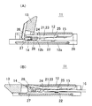
- Patent Document 1 discloses a connector having a structure as shown in FIGS. 1 (A) and 1 (B). Two types of contacts (connection terminals) are incorporated in the housing 12 of the connector 11.
- FIG. 2 shows one contact 21.
- the fixed piece 22 and the movable piece 23 are substantially parallel, and the fixed piece 22 and the movable piece 23 are connected to each other by a connecting portion 24 perpendicular to both pieces 22 and 23.
- a movable contact portion 25 is provided on the lower surface of the front end portion of the movable piece 23, and the rear end portion of the movable piece 23 is an operation receiving portion 26 that is acted on by the cam portion 14 of the connector 11.
- the retaining portion 28 protrudes from the upper surface of the fitting portion 27 formed at the rear portion of the fixed piece 22 at a position close to the connecting portion 24, and the fixing leg portion 29 protrudes from the lower surface of the front end portion of the fixed piece 22. ing.
- the contact 21 is inserted into the insertion hole 15 of the housing 12 from the front, and the back surface of the fixing leg 29 hits the front end of the base 12a of the housing 12 and stops.
- the fitting portion 27 is press-fitted between the base 12a and the holding portion 12b of the housing 12, and the lower surface of the fitting portion 27 is pressed against the base 12a by fitting the retaining portion 28 to the lower surface of the holding portion 12b. Stopped. Further, the cam portion 14 is inserted between the operation receiving portion 26 and the fitting portion 27 of the contact 21. The cam portion 14 is rotated by the operation lever 13.
- the flexible printed circuit board 16 When connecting the flexible printed circuit board 16 to the connector 11, the flexible printed circuit board 16 is inserted between the fixed piece 22 and the movable piece 23 in front of the connecting portion 24 as shown in FIG. Next, the operation lever 13 is tilted to rotate the cam portion 14, and the operation receiving portion 26 is pushed up by the cam portion 14. When the operation receiving portion 26 is pushed up, the movable contact portion 25 is lowered and pressed against the upper surface of the flexible printed circuit board 16. The flexible printed circuit board 16 is held between the movable contact portion 25 and the fixed piece 22 while being bent. In addition, the movable contact portion 25 is in pressure contact with the electrode pad of the flexible printed circuit board 16 so that the connector 11 and the flexible printed circuit board 16 are electrically connected.
- the connector 11 may be subject to vibration depending on the application. Further, the contact 21 may be subjected to a tensile force by the flexible printed circuit board 16 being held. Therefore, in such a connector 11, the possibility that the contacts 21 come out of the housing and gradually loosen cannot be wiped out.
- the contact 21 is electrically connected to the flexible printed circuit board 16 simply by pressing the movable contact section 25 to the electrode pad of the flexible printed circuit board 16, the electrical contact between the movable contact section 25 and the electrode pad is achieved. It is required to stabilize the contact.
- the present invention has been made in view of the technical problems as described above, and an object of the present invention is to provide a contact that can surely make electrical contact and mechanical contact with other members. There is to do. Moreover, it is providing the manufacturing method of the metal component containing the said contact.
- the contact according to the present invention is characterized in that a concave-convex shape comprising at least one of a concave stripe or a convex stripe is provided in a contact portion with another member.
- the contact pressure with the other member can be increased because the contact portion with the other member has an uneven shape. Therefore, electrical contact and mechanical contact can be ensured.
- the contact portion with another member for example, the contact portion is provided with a concavo-convex shape
- dirt or oxide film on the electrode surface of the other member can be destroyed by the concavo-convex shape, and the underlying electrode can be exposed.
- the reliability of manual contact can be improved.
- a contact portion with another member for example, a press contact portion
- the sliding resistance with the other member increases when the contact is fitted to the other member, and the contact loosens or falls off. Can be prevented.
- the contact portion with the other member is a contact portion, and the uneven shape extends in a direction perpendicular to the pressing direction and the wiping direction of the contact portion.
- the concavo-convex ridges are linearly abutted on the electrodes of other members and are wiped in a direction orthogonal to the direction of linear abutment. Therefore, since the linearly abutting ridge moves in a direction perpendicular to it and wipes the electrode surface in a planar shape, dirt and oxide film on the surface of the electrode pad can be efficiently destroyed, and the contact portion Contact reliability can be further improved.
- the contact portion with the other member is a pressure contact surface to the other member, and the uneven shape extends in a direction perpendicular to the insertion direction to the other member.
- the width is 250 ⁇ m or less, and the tips of the ridges constituting the concavo-convex shape are curved. According to this embodiment, the uneven contact pressure can be made extremely high.
- Still another embodiment of the contact according to the present invention has a width of 250 ⁇ m or less, and the ridges or ridges constituting the concavo-convex shape are continuous from one end to the other end in the width direction. According to such an embodiment, since the ridges or ridges are continuous from end to end, the contact with other members is stable, and the contact is less likely to tilt.
- Still another embodiment of the contact according to the present invention is provided with the uneven shape when produced by electroforming. According to this embodiment, it is possible to produce a fine uneven shape as compared with the case where the contact is produced by punching.
- a first manufacturing method of a metal part according to the present invention is a method of forming a resist film on the surface of an electrode plate, and using a photomask having a mask pattern in which fine irregularities are drawn on at least a part of an edge.
- the edge here may be an inner peripheral edge or an outer peripheral edge. According to the first manufacturing method of the present invention, it is possible to produce a concavo-convex shape on the surface of a metal part by the concavo-convex of the mask pattern formed on the photomask. Moreover, a desired uneven
- a second method for manufacturing a metal component according to the present invention includes a step of forming a resist film on a surface of an electrode plate, and a state in which fine particles are distributed between the resist film and a photomask.
- the second manufacturing method of the present invention it is possible to produce a concavo-convex shape on a metal part without using an expensive photomask, and the manufacturing cost of the metal part can be reduced.
- a third method for producing a metal part according to the present invention includes a step of disposing a dry film resist having a fine particle layer on a surface layer portion on a surface of an electrode plate, and exposing and developing the resist film to form the resist film.
- the method includes a step of opening a molding opening and a step of depositing an electroformed material in the molding opening by electroforming and shaping.
- a protective film containing a lubricant pasted on the surface of the dry film resist for preventing adhesion in the dry film production process and the distribution process can be used.
- the third manufacturing method of the present invention it is possible to produce a concavo-convex shape on a metal part without using an expensive photomask, and it is possible to use a protective film of a dry film resist. Can be cheap.
- the metal part, particularly the contact, according to the present invention is provided with a concave-convex shape including at least one of a concave line or a convex line on the surface by the first to third manufacturing methods of the metal part according to the present invention.
- a fine uneven shape can be imparted to the surface of the metal part manufactured by electroforming by a simple method.
- the connector according to the present invention is characterized in that the contact according to the present invention is housed in a housing. According to such a connector, the contact can be firmly incorporated in the housing, and the contact is difficult to be removed from the housing. In addition, the reliability of electrical contact with an electrode pad such as a flexible printed board is improved.
- the means for solving the above-described problems in the present invention has a feature in which the above-described constituent elements are appropriately combined, and the present invention enables many variations by combining such constituent elements. .
- FIGS. 1A and 1B are cross-sectional views showing a conventional connector.
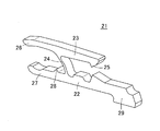
- FIG. 2 is a perspective view of a contact used in the connector of FIG.
- FIG. 3 is a perspective view of a contact according to an embodiment of the present invention in an upside down state.
- FIG. 4A is an enlarged perspective view showing a contact portion of the contact shown in FIG.
- FIG. 4B is an enlarged perspective view showing a fitting portion of the contact shown in FIG.
- FIG. 5A is a cross-sectional view of a connector using the contact of FIG.
- FIG. 5B is a cross-sectional view showing a state in which a flexible printed board is connected to the connector.
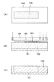
- FIGS. 6A, 6B, and 6C are cross-sectional views showing various surfaces provided with a concavo-convex shape.
- FIGS. 7A, 7B, and 7C are explanatory views of the operation of the contact shown in FIG. FIG. 8 shows a cross section of a metal part punched out by pressing.
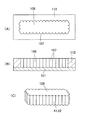
- FIG. 9A is a perspective view showing a concavo-convex pattern configured by convex ridges having a circular arc section that continuously extends from end to end along the width direction.
- FIG. 9B is a perspective view schematically showing the cut surface of FIG.
- FIG. 10A to FIG. 10C are schematic views showing a first manufacturing method for manufacturing a metal part having an uneven shape with an arcuate cross section.
- 11 (A) to 11 (C) are schematic views showing a first manufacturing method for manufacturing a metal part having an uneven shape with an arcuate cross section, and are a continuation of FIG.
- FIGS. 16A to 16C are schematic views showing a second manufacturing method for manufacturing a metal part having an uneven shape with an arcuate cross section.
- FIG. 17 (A) and 17 (B) are schematic views showing a second manufacturing method for manufacturing a metal part having an uneven shape with an arcuate cross section, and are a continuation of FIG. 16 (C). is there.
- 18 (A) to 18 (C) are schematic views showing a second manufacturing method for manufacturing a metal part having an uneven shape with an arcuate cross section, and are a continuation of FIG. 17 (B). is there.
- FIG. 19 shows a concavo-convex pattern of a resist formed by the second manufacturing method of metal parts.
- FIG. 20 is an enlarged view of a portion X in FIG.
- FIGS. 21A to 21C are schematic views showing a third manufacturing method for manufacturing a metal part having an uneven shape with an arcuate cross section.
- FIG. 22 (A) to 22 (D) are schematic views showing a third manufacturing method for manufacturing a metal part having an concavo-convex shape with an arcuate cross section, and are a continuation of FIG. 21 (C). is there.
- FIG. 23 is an external perspective view showing another connector according to the present invention. 24 is a cross-sectional view of the connector of FIG.
- FIG. 25 is a diagram showing a connection state between the connector and the battery of FIG. 23, FIG. 25A is a cross-sectional view of the state before connection, and FIG. 25B is a cross-sectional view of the state after connection.
- FIG. 3 is a perspective view of the contact 31 according to an embodiment of the present invention, and is shown in an upside down state.
- the contact 31 is a minute connection terminal manufactured by an electroforming method.
- 4A and 4B are enlarged views of a part of the contact 31.
- FIG. 5A is a sectional view of the connector 51 incorporating the contact 31, and
- FIG. 5B is a sectional view of the connector 51 to which the flexible printed circuit board 46 is connected.
- the fixed piece 32 and the movable piece 33 are substantially parallel, and the fixed piece 32 and the movable piece 33 are integrally connected by a connecting portion 34 that is substantially perpendicular to the two pieces 32 and 33.
- a movable contact portion 35 having a triangular shape protrudes from the lower surface of the front end portion of the movable piece 33, and the rear end portion of the movable piece 33 is an operation receiving portion 36 that receives an action from the cam portion of the connector 51.
- the front end portion of the fixed piece 32 is a fitting portion 37 that fits into the housing when the contact 31 is placed in the insertion hole of the housing 52.
- a protruding portion 38 protrudes from the upper surface of the fitting portion 37.
- a fixing leg 39 projects from the lower surface of the rear end of the fixing piece 32.
- a contact surface of the movable contact portion 35 that is in pressure contact with the electrode pad of the flexible printed circuit board that is, a contact contact surface 35a located on the lower surface of the movable contact portion 35
- a concavo-convex shape 41 including a plurality of ridges 41a or ridges 41b extending in a direction perpendicular to the pressing direction P and the wiping direction W is formed.
- the uneven shape 41 is generally a plurality of ridges or grooves extending continuously from one end to the other end along the width direction of the contact 31.
- the surface of the fitting portion 37 that contacts the housing that is, the press-contact surface 37a located on the lower surface, has a plurality of pieces extending in a direction perpendicular to the press-fitting direction S of the fitting portion 37 as shown in FIG.
- the concavo-convex shape 42 is formed of the ridge 42a or the ridge 42b.
- the uneven shape 42 is also generally a plurality of ridges or grooves extending continuously from one end to the other end along the width direction of the contact 31. Note that the uneven shape does not form the shape of a contact, and is a minute size compared to a minute contact.
- a connector 51 shown in FIGS. 5A and 5B incorporates a contact 31.
- This connector incorporates a plurality of two types of contacts.
- One contact is the contact 31.
- the contact 21 shown in FIG. 1 is provided with a concave / convex shape 41 on the contact surface of the movable contact portion 25 and the press contact surface of the fitting portion 27 in the contact 21 shown in FIG. A shape 42 is provided.
- the connector 51 may be substantially the same as the connector disclosed in Patent Document 1 except that the concave and convex shapes 41 and 42 are provided on both contacts. Therefore, the connector 51 will be briefly described with reference to FIGS. 5A and 5B (the description of Patent Document 1 is used for points not described here).
- the contact 31 is inserted into the insertion hole 55 of the housing 52 from the rear, and the front surface of the fixing leg 39 hits the rear end of the base 52a of the housing 52 and stops.
- the fitting portion 37 is press-fitted into the housing 52, and a pressure contact surface 37a (uneven shape 42) provided on the lower surface of the fitting portion 37 is in pressure contact with the upper surface of the base 52a, thereby preventing the contact 31 from coming off.
- a cam portion 54 is inserted between the operation receiving portion 36 of the contact 31 and the fixed piece 32. The cam portion 54 is rotated by the operation lever 53.
- the flexible printed circuit board 46 When connecting the flexible printed circuit board 46 to the connector 51, the flexible printed circuit board 46 is inserted between the fixed piece 22 and the movable piece 23 in front of the connecting portion 24 as shown in FIG. Next, the operation lever 53 is tilted to rotate the cam portion 54, and the operation receiving portion 36 is pushed up by the cam portion 54. When the operation receiving portion 36 is pushed up, the movable contact portion 35 is lowered and pressed against the upper surface of the flexible printed board 46. The flexible printed circuit board 46 is held between the movable contact portion 35 and the protrusion 38 while being bent in this manner. In addition, the movable contact portion 35 is in pressure contact with the electrode pad of the flexible printed circuit board 46, whereby the connector 51 and the flexible printed circuit board 46 are electrically connected.
- the position of the contact contact surface 35a (uneven shape 41) and the position of the pressure contact surface 37a (uneven shape 42) shown in FIG. 3 are examples and may be changed as appropriate. That is, since the positions of the movable contact portion 35 and the contact contact surface 35a change depending on the structure and type of the connector or the like incorporating the contact 31, the position of the concavo-convex shape 41 also changes accordingly. Further, since the position of the pressure contact surface 37a of the contact 31 also changes depending on the shape of the housing and the manner in which the contact 31 is incorporated into the housing, the position of the uneven shape 42 also changes accordingly. Accordingly, the concave and convex shapes 41 and 42 may be provided on a curved surface as shown in FIG. 6A, or may be provided on a flat surface as shown in FIG. 6B. In some cases, it is provided on a raised plane.
- the contact 31 can also be used for a terminal of a relay or a switch in addition to a connector.
- the contact part 35 can be contacted, and the contact reliability of the movable contact part 35 is improved.
- the ridge 41a is linear to the electrode pad 61. Wiping is performed in a direction perpendicular to the direction of linear contact. Therefore, since the ridge 41a in linear contact moves in a direction orthogonal to the surface and wipes the surface of the electrode pad in a planar shape, it is possible to efficiently destroy the dirt and oxide film on the surface of the electrode pad, The contact reliability of the movable contact portion 35 can be further improved.
- the press contact surface 37 a in contact with the housing 52 is provided with an uneven shape 42 extending in a direction orthogonal to the insertion direction of the contact 31, so that the contact area between the press contact surface 37 a and the housing 52 is reduced. Can be small. Therefore, the contact pressure of the pressure contact surface 37a (or the uneven shape 42) can be increased. As a result, for example, as shown in FIG. 7B, when the contact 31 is press-fitted into the insertion hole 63 of the mating member 62, the sliding resistance between the contact 31 and the housing 52 is increased to increase the holding force of the contact 31. The contact 31 is loosened and it is difficult to remove from the housing 52.
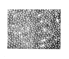
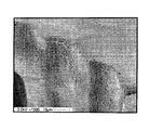
- FIG. 8 shows a micrograph of a cross section when punched from a metal plate by pressing.
- a streak-like shear surface and a fracture surface where the structure is crushed appear, and the streaks of the shear surface are interrupted at the fracture surface.
- the thickness of the metal plate is D1 and the length (thickness) of the shear plane is D2
- the value of D2 / D1 is 1/2 or more and 1/3 or less.
- the contact width is 250 ⁇ m or less, and the surface is arcuate or continuous from one end (one side surface) to the other end (other side surface) in the width direction.
- a convex surface 71 having a circular arc surface (a semicircular cross section) is extended from end to end, and a contact surface having an uneven shape in which it is arranged at an average pitch s. Thought. This is called model M1.
- V-groove-shaped ridges 72 (or ridges having a trapezoidal cross section) are arranged at an average pitch s, and the surface 73 is flat at one end. I thought about the surface.
- the model M2 is obtained by modeling a cross section by pressing as shown in FIG. FIG. 9C shows a case where the speeding surface is smooth. This is called model M3.
- Condition 1 is as follows. Average pitch of irregularities s: 0.1 mm Load (pressing force) F: 100 gf Contact width L: 0.05 mm Thickness t: 0.1mm Curvature radius R: 0.002mm
- the contact pressure of the model M1 provided at the pitch of 71 was 71 times that of the model M3. According to Hertz's formula, the uneven contact pressure formed by the arcuate ridges is greater than the contact pressure of the part formed by pressing.
- the uneven shape of the contact has a semicircular arc-shaped cross-section formed continuously from end to end on a metal plate having a width of 25 ⁇ m or less.
- a contact having such a concavo-convex shape, generally speaking, a metal plate can be produced by electroforming as follows.
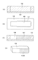
- FIGS. 10A to 10C, 11A to 11C, and 12A to 12D show a first method for manufacturing a metal part by electroforming.
- FIGS. 10A, 10B, 11B, 11C, 12B, and 12C are cross-sectional views.
- FIG. 10C is a plan view of FIG.
- FIG. 11A is a bottom view of the photomask illustrated in FIG.
- FIG. 12A is a plan view of FIG.
- FIG. 12D is a perspective view of a metal part.
- a negative resist is applied to the upper surface of the electrode plate 101 for electroforming to form a resist film 102.
- the electrode plate 101 is a conductive substrate, and is formed by coating a conductive material on the surface of a metal plate, a plate made of a conductive material, or a plate made of a non-conductive material.
- fine particles 103 are distributed on the upper surface of the resist film 102 at an appropriate density to form a fine particle layer.
- the region in which the fine particles 103 are distributed may be the entire upper surface of the resist film 102 or a part thereof.
- the fine particles may be those that shield light such as metal fine particles and ceramic fine particles, and may be transparent materials that scatter light such as glass particles.
- a transparent sheet containing fine particles may be attached to the upper surface of the resist film 102, fine particles dispersed in a resist solution may be applied to the upper surface of the resist film 102, and powdery fine particles (powder) ) May be dispersed on the upper surface of the resist film 102.
- a photomask 104 is overlaid on the resist film 102 having a fine particle layer formed on the surface.
- a mask pattern 105 (light shielding region) as shown in FIG. 11A is formed on the lower surface of the photomask 104. Since it is not necessary to design fine irregularities around the mask pattern 105, the mask cost can be reduced.
- the resist film 102 is exposed through the photomask 104 as shown in FIG. 11B, light passes through the photomask 104 in the region where the mask pattern 105 is not provided, and the resist film 102 is exposed. At the same time, the light transmitted through the photomask 104 is also blocked by the fine particles 103. Therefore, even if the edge of the mask pattern 105 is smooth as shown in FIG. Arise.
- the resist in the exposed area is insolubilized.
- an insoluble resist is indicated by a solid line hatching
- a soluble resist is indicated by a broken line hatching. Therefore, when the resist film 102 is developed after the fine particles 103 are removed, as shown in FIGS. 12A and 12B, the resist film 102 in the light shielding region is removed leaving only the resist film 102 in the exposure region. A cavity 106 is opened in the resist film 102. At this time, an uneven pattern 107 having an arc-shaped cross section extending in the vertical direction is formed on the wall surface of the cavity 106 by the shadow of the fine particles 103.
- an electroformed material 108 is grown in the cavity 106 of the resist film 102 by an electroforming method and formed into a predetermined shape.
- the electroforming material 108 to be used is mainly composed of any one of Ni, Co, Fe, Cu, Mn, Sn, and Zn, and may be an alloy thereof.
- the electroformed material 64 has grown to a sufficient thickness, the electroforming process is completed.
- the metal part 109 is, for example, a contact, and uneven shapes 41 and 42 extending continuously from end to end along the width direction of the metal part 109 are formed on the whole or a part of the outer peripheral surface.
- the metal part 109 and the concavo-convex shapes 41 and 42 are formed by the electroforming method, a mask pattern having a simple shape can be used, so that the manufacturing cost can be reduced.
- FIG. 13 is a photomicrograph of the state when fine particles having a diameter of 28 ⁇ m are applied to the surface of the resist film.
- FIG. 14 is an SEM photograph of a negative resist film that has been exposed and developed through the fine particle layer. It can be seen that a striped uneven pattern is formed on the wall surface of the cavity.
- FIG. 15 shows a concavo-convex pattern formed on the wall surface of the resist film when the particle diameter of the fine particles is changed in the range of 0 ⁇ m to about 30 ⁇ m (where the particle diameter is 0 ⁇ m when no fine particles are present).
- This shows the result of actual measurement of how the pitch changes. According to this measurement result, it can be seen that the pitch of the concavo-convex pattern is substantially proportional to the particle diameter. Therefore, it is possible to obtain the uneven shapes 41 and 42 having a substantially desired pitch by adjusting the particle diameter.
- FIGS. 16A to 16C A second method for manufacturing a metal part by electroforming is shown in FIGS. 16A to 16C, 17A, 17B, and 18A to 18C.
- FIGS. 16A, 17A, 17B, and 18B are cross-sectional views.
- FIG. 16B is a plan view of FIG.
- FIG. 16C is a bottom view of the photomask illustrated in FIG.
- FIG. 18A is a plan view of FIG.
- FIG. 18C is a perspective view of a metal part.
- a dry film resist is used.
- a dry film resist is affixed on a base film, and further a protective film is affixed on the dry film resist.
- a protective film is affixed on the dry film resist.
- fine particles called a lubricant are mixed in the protective film.
- the dry film resist 111 from which the base film has been peeled is applied to the upper surface of the electrode plate 101 for electroforming. Adhere closely. Therefore, when the dry film resist 111 is provided on the upper surface of the electrode plate 101, the lubricant 113 (fine particles) is distributed in the transparent protective film 112 thereon.
- a photomask 104 is overlaid on the protective film 112.
- a mask pattern 105 (light shielding region) as shown in FIG. 16C is formed on the lower surface of the photomask 104.
- the dry film resist 111 is exposed to light through the photomask 104 and the protective film 112 as shown in FIG. 17A, it is shielded by the lubricant 113, so that the edge of the mask pattern 105 is smooth as shown in FIG.
- irregularities occur at the edge of the light shielding region of the protective film 112.
- the resist in the exposed area is insolubilized as shown in FIG. Therefore, when the resist film 102 is developed after the protective film 112 is peeled off, as shown in FIGS. 18 (A) and 18 (B), the protective film 112 in the light shielding area is removed, leaving only the exposed area 112, and the protection film 112 is protected.
- a cavity 106 is opened in the film 112. At this time, an uneven pattern 107 having an arc-shaped cross section extending in the vertical direction is formed on the wall surface of the cavity 106 by the shadow of 113.
- FIG. 19 is an SEM photograph of the end face of the metal part manufactured by the second manufacturing method.
- FIG. 20 is an enlarged photograph of the portion X in FIG. In this example, exposure and development are performed while leaving the protective film on the dry film resist, and a metal part is manufactured by electroforming, and the uneven shape caused by the lubricant of the protective film is shown.
- FIGS. 21A, 21C, 22A, and 22C are cross-sectional views.
- FIG. 21B is a bottom view of the photomask shown in FIG.
- FIG. 22B is a plan view of FIG.
- FIG. 22D is a perspective view of a metal part.
- a negative resist is applied to the upper surface of the electrode plate 101 for electroforming to form a resist film 102.
- a photomask 104 is overlaid on the resist film 102.
- a mask pattern 105 (light shielding region) as shown in FIG. 21B is formed on the lower surface of the photomask 104.
- fine irregularities 115 are designed on a part or the whole of the outer periphery. Note that although the unevenness 115 is exaggerated in FIG. 21B, the unevenness 115 is a fine pattern as compared with the size of the mask pattern 105.
- the resist in the exposed area is insolubilized as shown in FIG. Therefore, when the resist film 102 is developed, as shown in FIGS. 22B and 22C, the resist film 102 in the light shielding region is removed leaving only the resist film 102 in the exposure region, and the cavity 106 is formed in the resist film 102. Is opened. At this time, an uneven pattern 107 having an arc-shaped cross section extending in the vertical direction is formed on the wall surface of the cavity 106 by the unevenness 115 of the mask pattern 105.
- an electroformed material is grown in the cavity 106 of the resist film 102 by an electroforming method to manufacture a metal part 109 having a predetermined shape.
- the metal part 109 is, for example, a contact, and uneven shapes 41 and 42 extending continuously from end to end along the width direction of the metal part 109 are formed on the whole or a part of the outer peripheral surface.
- the metal part 109 and the concavo-convex shapes 41 and 42 are formed by the electroforming method, a mask pattern having a simple shape can be used, so that the manufacturing cost can be reduced.
- the irregular shapes 41 and 42 having an arbitrary shape can be formed.
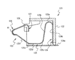
- the connector 121 is a connector for charging by contacting an electrode pad of a battery used in, for example, a portable electronic device.
- FIG. 23 is a perspective view showing the connector 121
- FIG. 24 is a sectional view of the connector.
- the connector 121 has a plurality of contacts 123 housed in a connector housing 122 and a part of the contacts 123 projecting from the front surface of the connector housing 122. As shown in FIG.
- the contact 123 includes a fixing part 124, an elastic part 125, a contact part 126, and a latching part 127.
- the fixing portion 124 of the contact 123 includes a contact tail 124a extending in the horizontal direction at the rear end portion, and a holding portion 124b that is bent vertically upward from the contact tail 124a and extends upward.
- the contact tail 124a is electrically connected to a printed wiring board on which the connector 121 is mounted.
- the contact 123 is fixed to the connector housing 122 by a contact tail 124a.
- the elastic portion 125 of the contact 123 includes a first bending portion 125a that is curved in a U shape from the upper end of the fixing portion 124, a first connection portion 125b that extends downward from the first bending portion 125a, and a first connection portion 125b.
- a second bending portion 125c that curves in the horizontal and forward directions from the lower end of the first connection portion, a second connection portion 125d that extends in the horizontal and forward directions from the front end of the second bending portion 125c, and a diagonally upward direction from the front end of the second connection portion 125d.
- a third bending portion 125e that curves toward the front, and an extension portion 125f that extends obliquely forward and upward from the front end of the third bending portion 125e.
- the elastic portion 125 has a substantially S shape, and the contact 123 can generate a sufficient urging force in the front-rear direction.
- the contact portion 126 of the contact 123 curves backward from the front end of the extension portion 125f of the elastic portion 125 in a substantially U shape or arc shape, and this curved surface forms a contact portion 23a.
- the contact portion 126 is formed with concavo-convex shapes 41 formed of ridges having a cross-sectional arc shape continuous from one end to the other end along the width direction. It should be noted that the vicinity of the contact portion 23a of the contact portion 126 is narrower than the other portions.
- the latching portion 127 of the contact 123 is formed to be folded further downward from the end portion of the contact portion 126, and the latching portion 127 is latched to the contact support portion 128 provided at the opening of the connector housing 122. Has been.
- This connector 121 is to be in contact with a battery 129 for portable equipment as shown in FIGS. 25 (A) and 25 (B). That is, when the battery 129 is pressed against the connector 121, the contact portion 126 provided with the uneven shape 41 comes into contact with the electrode 130 of the battery 129 and bends, and a charging current is supplied from the connector 121 to the battery 129.
Landscapes
- Engineering & Computer Science (AREA)
- Manufacturing & Machinery (AREA)
- Coupling Device And Connection With Printed Circuit (AREA)
- Manufacturing Of Electrical Connectors (AREA)
Abstract
Description
そのため、このようなコネクタ11においては、コンタクト21がハウジングから抜けて徐々に緩んでくるおそれを払拭することができない。
図3は、本発明の一実施形態によるコンタクト31の斜視図であって、上下を反転させた状態で表している。このコンタクト31は、電鋳法によって作製される微小な接続端子である。図4(A)及び図4(B)は、コンタクト31の一部を拡大した図である。また、図5(A)は当該コンタクト31を組み込んだコネクタ51の断面図、図5(B)はフレキシブルプリント基板46を接続されたコネクタ51の断面図である。
図5(A)及び図5(B)に示すコネクタ51は、コンタクト31を組み込んだものである。このコネクタには、2種類のコンタクトがそれぞれ複数本組み込まれている。一方のコンタクトは、上記コンタクト31である。他方のコンタクトは、図1に示したコンタクト21において、図3のコンタクト31と同様に、その可動接点部25の接点接触面に凹凸形状41を設け、またその嵌合部27の圧接面に凹凸形状42を設けたものである。
つぎに、コンタクト31に凹凸形状41、42を設けることによる効果を説明する。このコンタクト31では、可動接点部35の接触面に凹凸形状41を形成しているので、可動接点部35の接触圧が凸条41aの先端に集中し、可動接点部35の接触圧が大きくなり、可動接点部35の接触信頼性が向上する。また、可動接点部35に凹凸形状41を設けていると、フレキシブルプリント基板46の電極パッド表面に生じている汚れや酸化膜が凸条41aによって破壊され、露出させた電極パッドの金属面に可動接点部35を接触させることができ、可動接点部35の接触信頼性が向上する。特に、図7(A)に示すように、凹凸形状41が可動接点部35の押圧方向P及びワイピング方向Wに垂直な方向に延びている場合には、凸条41aが電極パッド61に線状に当接して線状に当接している方向と直交する方向へワイピングされる。よって、線状に当接した凸条41aがそれと直交する方向へ移動して電極パッドの表面を面状にワイピングするので、電極パッドの表面の汚れや酸化膜を効率よく破壊することができ、可動接点部35の接触信頼性をより一層向上させることができる。
この効果を得るためには、図7(B)に示すように嵌合部37の全面に凹凸形状42を設ける必要はなく、図7(C)に示すように、嵌合部37の一部の面だけに凹凸形状42を設けていてもよい。
つぎに、好ましい凹凸形状について説明する。コンタクトは、一般に、金属板を打ち抜くことによって作製されることが多い。プレスにより金属板から打ち抜いたときの断面の顕微鏡写真を図8に示す。金属板をプレスで打ち抜いたときの断面には、筋状の剪断面と組織が潰れたような破断面とが表れていて、剪断面の筋が破断面で途切れている。ここで、金属板の厚みをD1、剪断面の長さ(厚み)をD2とすると、一般的には、D2/D1の値が1/2以上1/3以下である。このようなプレスによる断面をコンタクトの接触面として使用した場合には、相手部材に接触したときにコンタクトが片当たりして傾く。また、相手部材との接触も不安定になる。そのため、プレスによる断面はコンタクトの接触面としては好ましくない。
図9(A)のような円弧状の凹凸形状を有するモデルM1では、線接触のために接触圧が大きくなるので、ヘルツ(Hertz)理論(たとえば、NACHI-BUISINESS news, Vol.10D1, June 2006; 株式会社不二越 開発本部 開発企画部 2006年6月20日発行)を用いて接触圧を計算した。
円弧状の凸条が1本であれば、凸条(円筒)と平面の接触時の面圧は次の数式1で表される。

F:荷重(加圧力)
E:縦弾性係数
t:板厚
R:凸条の表面の曲率半径
である。

F:荷重
E:縦弾性係数
t:板厚
R:凸条の表面の曲率半径
f:凸条1本当たりにかかる力
n:凸条の本数
L:接触幅
s:凹凸の平均ピッチ
であって、f=F/n、L=n×s である。

F:荷重
t:板厚
L:接触幅
である。

F:荷重
t:板厚
L:接触幅
である。
凹凸の平均ピッチ s: 0.1mm
荷重(加圧力) F: 100gf
接触幅 L: 0.05mm
板厚 t: 0.1mm
曲率半径 R: 0.002mm
ヤング率とポアソン比については、コネクタ材料として最も多く用いられる「りん青銅」の値を使用した。
ヤング率E=1.2×10⁵[N/mm2]
ポアソン比=0.3
この条件1は、大きな接触力を想定した条件である。この結果は次の表1の通りであった。

凹凸の平均ピッチ s: 0.004mm
荷重(加圧力) F: 10gf
接触幅 L: 10mm
板厚 t: 0.25mm
曲率半径 R: 0.025mm
ここでもヤング率とポアソン比については、コネクタ材料として最も多く用いられる「りん青銅」の上記値を使用した。
この結果は次の表2の通りであった。

以上述べたように、コンタクトの凹凸形状は25μm以下の幅の金属板に対して端から端まで連続的に形成された断面半円弧状の凸条を有するものが好ましい。このような凹凸形状を有するコンタクト、一般的にいえば金属板は、以下のようにして電鋳法で作製することができる。
図10(C)は図10(B)の平面図である。図11(A)は図11(B)に示すフォトマスクの下面図である。図12(A)は図12(B)の平面図である。図12(D)は金属部品の斜視図である。
電鋳法による金属部品の第2の製造方法を図16(A)-図16(C)、図17(A)、図17(B)及び図18(A)-図18(C)に示す。ここで、図16(A)、図17(A)、図17(B)及び図18(B)は断面図である。図16(B)は図16(A)の平面図である。図16(C)は図17(A)に示すフォトマスクの下面図である。図18(A)は図18(B)の平面図である。図18(C)は金属部品の斜視図である。
電鋳法による金属部品の第3の製造方法を図21(A)-図21(C)及び図22(A)-図22(D)に示す。ここで、図21(A)、図21(C)、図22(A)及び図22(C)は断面図である。図21(B)は図21(C)に示すフォトマスクの下面図である。図22(B)は図22(C)の平面図である。図22(D)は金属部品の斜視図である。
このマスクパターン105には、外周の一部又は全体に微細な凹凸115がデザインされている。なお、図21(B)では凹凸115は誇張して描いているが、マスクパターン105の大きさと比較しても凹凸115は微細なパターンである。図21(C)のようにフォトマスク104を通してレジスト膜102に露光すると、マスクパターン105の設けられていない領域ではフォトマスク104を光が透過してレジスト膜102が露光される。
つぎに、本発明に係る別な形態のコンタクトとコネクタを説明する。このコネクタ121は、たとえば携帯用電子機器に使用されるバッテリーの電極パッドに接触させて充電を行わせるためのコネクタである。図23は、当該コネクタ121を示す斜視図であって、図24は当該コネクタの断面図である。
また、コンタクト123は、コンタクトテール124aによってコネクタハウジング122に固定されている。
なお、コンタクト部126の接触部23a付近は他の部分に比べて幅狭となっている。
32 固定片
33 可動片
34 連結部
35 可動接点部
35a 接点接触面
37 嵌合部
37a 圧接面
41 凹凸形状
42 凹凸形状
46 フレキシブルプリント基板
51 コネクタ
101 電極板
102 レジスト膜
103 微粒子
104 フォトマスク
111 ドライフィルムレジスト
112 保護フィルム
113 滑剤
Claims (12)
- 他部材との接触部に、凹条又は凸条の少なくとも一方からなる凹凸形状を設けたことを特徴とするコンタクト。
- 前記他部材との接触部が接点部であって、
前記凹凸形状は、当該接点部の押圧方向及びワイピング方向に垂直な方向に延伸していることを特徴とする、請求項1に記載のコンタクト。 - 前記他部材との接触部が他部材への圧接面であって、
前記凹凸形状は、前記他部材への挿入方向に垂直な方向に延伸していることを特徴とする、請求項1に記載のコンタクト。 - 幅が250μm以下であって、
前記凹凸形状を構成する凸条の先端が湾曲していることを特徴とする、請求項1に記載のコンタクト。 - 幅が250μm以下であって、
前記凹凸形状を構成する凸条又は凹条が幅方向の一端から他端まで連続していることを特徴とする、請求項1に記載のコンタクト。 - 電鋳法によって作製する際に、前記凹凸形状を設けられていることを特徴とする、請求項1に記載のコンタクト。
- 電極板の表面にレジスト膜を形成する工程と、
縁の少なくとも一部に微細な凹凸が描かれたマスクパターンを有するフォトマスクを用いて前記レジスト膜に露光する工程と、
前記レジスト膜を現像して前記レジスト膜に成形用開口をあける工程と、
前記成形用開口内に電鋳法によって電鋳材料を堆積させて賦形する工程と、
を有することを特徴とする金属部品の製造方法。 - 電極板の表面にレジスト膜を形成する工程と、
前記レジスト膜とフォトマスクとの間に微粒子群を分布させた状態で、前記レジスト膜に露光する工程と、
前記レジスト膜を現像して前記レジスト膜に成形用開口をあける工程と、
前記成形用開口内に電鋳法によって電鋳材料を堆積させて賦形する工程と、
を有することを特徴とする金属部品の製造方法。 - 表層部に微粒子層を有するドライフィルムレジストを電極板の表面に配設する工程と、 前記レジスト膜に露光及び現像を行って前記レジスト膜に成形用開口をあける工程と、 前記成形用開口内に電鋳法によって電鋳材料を堆積させて賦形する工程と、
を有することを特徴とする金属部品の製造方法。 - 請求項7から9のうちいずれか1項に記載した製造方法により、凹条又は凸条の少なくとも一方からなる凹凸形状を表面に設けられた金属部品。
- 請求項7から9のうちいずれか1項に記載した製造方法により、凹条又は凸条の少なくとも一方からなる凹凸形状を表面に設けられたコンタクト。
- 請求項1又は11に記載した、コンタクトをハウジング内に納めたことを特徴とするコネクタ。
Priority Applications (3)
| Application Number | Priority Date | Filing Date | Title |
|---|---|---|---|
| US13/266,936 US8678851B2 (en) | 2011-03-15 | 2011-03-24 | Contact section having an irregular shape formed thereon by electroforming |
| KR1020117024221A KR101324350B1 (ko) | 2011-03-15 | 2011-03-24 | 콘택트 및 금속 부품의 제조 방법 |
| CN201180001912.5A CN102870283B (zh) | 2011-03-15 | 2011-03-24 | 接触件及金属部件的制造方法 |
Applications Claiming Priority (2)
| Application Number | Priority Date | Filing Date | Title |
|---|---|---|---|
| JP2011-057073 | 2011-03-15 | ||
| JP2011057073A JP4924854B1 (ja) | 2011-03-15 | 2011-03-15 | コンタクト及び金属部品の製造方法 |
Publications (1)
| Publication Number | Publication Date |
|---|---|
| WO2012124167A1 true WO2012124167A1 (ja) | 2012-09-20 |
Family
ID=46243845
Family Applications (1)
| Application Number | Title | Priority Date | Filing Date |
|---|---|---|---|
| PCT/JP2011/057160 WO2012124167A1 (ja) | 2011-03-15 | 2011-03-24 | コンタクト及び金属部品の製造方法 |
Country Status (6)
| Country | Link |
|---|---|
| US (1) | US8678851B2 (ja) |
| JP (1) | JP4924854B1 (ja) |
| KR (1) | KR101324350B1 (ja) |
| CN (1) | CN102870283B (ja) |
| TW (1) | TWI456842B (ja) |
| WO (1) | WO2012124167A1 (ja) |
Families Citing this family (5)
| Publication number | Priority date | Publication date | Assignee | Title |
|---|---|---|---|---|
| US8827733B2 (en) * | 2011-03-15 | 2014-09-09 | Omron Corporation | Connecting terminal with a fixed portion and a contact |
| JP6497075B2 (ja) * | 2015-01-09 | 2019-04-10 | オムロン株式会社 | 電気機器システム |
| US10169649B2 (en) | 2016-07-28 | 2019-01-01 | International Business Machines Corporation | Smart image filtering method with domain rules application |
| EP3471220A1 (en) * | 2017-10-16 | 2019-04-17 | TE Connectivity Germany GmbH | Bent electric contact element with chamfered edges and method for its manufacture |
| CN110350338A (zh) * | 2019-08-07 | 2019-10-18 | 苏州祥龙嘉业电子科技股份有限公司 | 一种电连接器端子 |
Citations (6)
| Publication number | Priority date | Publication date | Assignee | Title |
|---|---|---|---|---|
| JPS516694Y1 (ja) * | 1969-03-12 | 1976-02-24 | Matsushitaden Koukabushikigaishiya | |
| JPS5464286U (ja) * | 1978-10-06 | 1979-05-07 | ||
| JPS5595279A (en) * | 1979-01-13 | 1980-07-19 | Matsushita Electric Works Ltd | Blade retaining spring |
| JPH048287U (ja) * | 1990-05-08 | 1992-01-24 | ||
| JP2002158056A (ja) * | 2000-09-11 | 2002-05-31 | Japan Aviation Electronics Industry Ltd | 電気接点部材およびその製造方法 |
| JP2002198115A (ja) * | 2000-12-22 | 2002-07-12 | Matsushita Electric Works Ltd | コネクタ |
Family Cites Families (25)
| Publication number | Priority date | Publication date | Assignee | Title |
|---|---|---|---|---|
| JPS516694A (ja) * | 1974-07-05 | 1976-01-20 | Suwa Seikosha Kk | Denkihatsushokuhyojitai |
| US4026013A (en) * | 1976-03-17 | 1977-05-31 | Amp Incorporated | Method and structure for terminating fine wires |
| US4802862A (en) * | 1981-03-30 | 1989-02-07 | North American Specialties Corporation | Solderable electrical contact |
| US4579413A (en) * | 1984-06-29 | 1986-04-01 | Amp Incorporated | Connector for the mass termination of small gauge magnet wire |
| US4572603A (en) * | 1984-06-29 | 1986-02-25 | Amp, Incorporated | Connector for terminating small gauge magnet wire |
| US4662702A (en) * | 1984-11-15 | 1987-05-05 | Daiichi Denshi Kagyo Kabushiki Kaisha | Electric contacts and electric connectors |
| JPS6469929A (en) | 1987-09-11 | 1989-03-15 | Matsushita Electric Ind Co Ltd | Semiconductor pressure sensor |
| JPH01103280U (ja) * | 1987-12-28 | 1989-07-12 | ||
| JPH0247985A (ja) | 1988-08-09 | 1990-02-16 | Matsushita Electric Ind Co Ltd | 映像信号ディジタル伝送方法 |
| JPH048287A (ja) | 1990-04-26 | 1992-01-13 | Fa Veda | 離解酵素製品および亜麻処理方法 |
| US5112233A (en) | 1991-05-30 | 1992-05-12 | Thomas & Betts Corporation | Electrical connector having contact retention means |
| JPH07263100A (ja) * | 1994-03-24 | 1995-10-13 | Kawasaki Steel Corp | 半導体装置用ソケット |
| US5624273A (en) * | 1995-04-21 | 1997-04-29 | The Whitaker Corporation | Insulation displacement contact with strain relief |
| JP3794514B2 (ja) * | 1996-07-31 | 2006-07-05 | ザ ウィタカー コーポレーション | 電気コネクタ |
| JPH11250966A (ja) * | 1997-12-22 | 1999-09-17 | Whitaker Corp:The | コネクタ |
| JP2001102141A (ja) * | 1999-07-27 | 2001-04-13 | Mitsubishi Electric Corp | テスト用ソケット、その製造方法、テスト用ソケットを用いたテスト方法、及び被テスト部材 |
| JP4026281B2 (ja) * | 1999-08-06 | 2007-12-26 | 三菱電機株式会社 | テスト用ソケット、その製造方法、およびテスト用ソケットを用いたテスト方法 |
| US6888362B2 (en) * | 2000-11-09 | 2005-05-03 | Formfactor, Inc. | Test head assembly for electronic components with plurality of contoured microelectronic spring contacts |
| JP2002071748A (ja) * | 2000-08-28 | 2002-03-12 | Mitsubishi Electric Corp | テスト用ソケット、このテスト用ソケットを用いたテスト方法、及び被テスト部材 |
| JP2004022248A (ja) * | 2002-06-13 | 2004-01-22 | Quasar System Inc | ソケット |
| JP4532308B2 (ja) * | 2005-02-21 | 2010-08-25 | 株式会社アイペックス | 電気コネクタの接続端子 |
| KR100868567B1 (ko) * | 2005-06-30 | 2008-11-13 | 주식회사 히타치엘지 데이터 스토리지 코리아 | 터미널 및 이를 사용한 커넥터 |
| JP2007073296A (ja) | 2005-09-06 | 2007-03-22 | D D K Ltd | 整列コンタクト群およびフレキシブル基板用電気コネクタ |
| JP5526522B2 (ja) | 2008-10-01 | 2014-06-18 | オムロン株式会社 | コネクタ用接続端子およびそれを用いたコネクタ |
| JP4832557B2 (ja) * | 2009-07-15 | 2011-12-07 | 本多通信工業株式会社 | 電気コネクタにおけるコンタクトの接触構造 |
-
2011
- 2011-03-15 JP JP2011057073A patent/JP4924854B1/ja active Active
- 2011-03-24 WO PCT/JP2011/057160 patent/WO2012124167A1/ja active Application Filing
- 2011-03-24 CN CN201180001912.5A patent/CN102870283B/zh active Active
- 2011-03-24 KR KR1020117024221A patent/KR101324350B1/ko active IP Right Grant
- 2011-03-24 US US13/266,936 patent/US8678851B2/en active Active
- 2011-10-12 TW TW100136858A patent/TWI456842B/zh active
Patent Citations (6)
| Publication number | Priority date | Publication date | Assignee | Title |
|---|---|---|---|---|
| JPS516694Y1 (ja) * | 1969-03-12 | 1976-02-24 | Matsushitaden Koukabushikigaishiya | |
| JPS5464286U (ja) * | 1978-10-06 | 1979-05-07 | ||
| JPS5595279A (en) * | 1979-01-13 | 1980-07-19 | Matsushita Electric Works Ltd | Blade retaining spring |
| JPH048287U (ja) * | 1990-05-08 | 1992-01-24 | ||
| JP2002158056A (ja) * | 2000-09-11 | 2002-05-31 | Japan Aviation Electronics Industry Ltd | 電気接点部材およびその製造方法 |
| JP2002198115A (ja) * | 2000-12-22 | 2002-07-12 | Matsushita Electric Works Ltd | コネクタ |
Also Published As
| Publication number | Publication date |
|---|---|
| CN102870283B (zh) | 2015-12-16 |
| KR20120115930A (ko) | 2012-10-19 |
| TW201238159A (en) | 2012-09-16 |
| KR101324350B1 (ko) | 2013-11-01 |
| TWI456842B (zh) | 2014-10-11 |
| JP2012195108A (ja) | 2012-10-11 |
| US8678851B2 (en) | 2014-03-25 |
| JP4924854B1 (ja) | 2012-04-25 |
| CN102870283A (zh) | 2013-01-09 |
| US20130045617A1 (en) | 2013-02-21 |
Similar Documents
| Publication | Publication Date | Title |
|---|---|---|
| JP4676502B2 (ja) | 基板対基板コネクタ | |
| JP4924854B1 (ja) | コンタクト及び金属部品の製造方法 | |
| US8647129B2 (en) | Housingless connector | |
| JP5472272B2 (ja) | 同軸コネクタプラグ及びその製造方法 | |
| US10998655B2 (en) | Connector and connection system | |
| JPH08190968A (ja) | コンタクト部材として金属ストリップを有するコネクタおよびこのコネクタを備えるコネクタ組立体 | |
| JPH07326416A (ja) | 端子及びコネクタ | |
| JP5526522B2 (ja) | コネクタ用接続端子およびそれを用いたコネクタ | |
| JP2010086877A (ja) | コネクタ用接続端子およびそれを組み込んだコネクタ | |
| JPH09259988A (ja) | 電気コネクタのターミナル | |
| JP4924856B1 (ja) | コンタクト及びコンタクトの製造方法 | |
| JP4821935B1 (ja) | 金属部品の製造方法 | |
| JP5451244B2 (ja) | Icカード用コネクタ | |
| CN205069919U (zh) | 电连接器 | |
| WO2015063818A1 (ja) | ソケット、そのソケットを備えるコネクタ、およびそのコネクタに用いられるヘッダ | |
| CN205070061U (zh) | 电连接器 | |
| JP2015204227A (ja) | フレキシブル基板接続用コネクタ | |
| JP2007165066A (ja) | シールド付fpcアダプタ | |
| JP2018503963A (ja) | 電気接点 | |
| JP2007294188A (ja) | 端子構造及び端子の製造方法 | |
| JP2015005469A (ja) | コネクタ及びコネクタを備えた携帯端末 | |
| WO2021131593A1 (ja) | 雄端子 | |
| JP2595483Y2 (ja) | 電気コネクタ | |
| JP3041579B2 (ja) | コンタクト | |
| US20180076545A1 (en) | Connector terminals with improved solder joint |
Legal Events
| Date | Code | Title | Description |
|---|---|---|---|
| WWE | Wipo information: entry into national phase |
Ref document number: 201180001912.5 Country of ref document: CN |
|
| ENP | Entry into the national phase |
Ref document number: 20117024221 Country of ref document: KR Kind code of ref document: A |
|
| WWE | Wipo information: entry into national phase |
Ref document number: 13266936 Country of ref document: US |
|
| 121 | Ep: the epo has been informed by wipo that ep was designated in this application |
Ref document number: 11860983 Country of ref document: EP Kind code of ref document: A1 |
|
| NENP | Non-entry into the national phase |
Ref country code: DE |
|
| 122 | Ep: pct application non-entry in european phase |
Ref document number: 11860983 Country of ref document: EP Kind code of ref document: A1 |