WO2012120913A1 - 積層セラミック電子部品およびその製造方法 - Google Patents
積層セラミック電子部品およびその製造方法 Download PDFInfo
- Publication number
- WO2012120913A1 WO2012120913A1 PCT/JP2012/050053 JP2012050053W WO2012120913A1 WO 2012120913 A1 WO2012120913 A1 WO 2012120913A1 JP 2012050053 W JP2012050053 W JP 2012050053W WO 2012120913 A1 WO2012120913 A1 WO 2012120913A1
- Authority
- WO
- WIPO (PCT)
- Prior art keywords
- internal electrode
- film
- multilayer ceramic
- electronic component
- ceramic electronic
- Prior art date
- Legal status (The legal status is an assumption and is not a legal conclusion. Google has not performed a legal analysis and makes no representation as to the accuracy of the status listed.)
- Ceased
Links
Images


Classifications
-
- H—ELECTRICITY
- H01—ELECTRIC ELEMENTS
- H01G—CAPACITORS; CAPACITORS, RECTIFIERS, DETECTORS, SWITCHING DEVICES, LIGHT-SENSITIVE OR TEMPERATURE-SENSITIVE DEVICES OF THE ELECTROLYTIC TYPE
- H01G4/00—Fixed capacitors; Processes of their manufacture
- H01G4/002—Details
- H01G4/005—Electrodes
- H01G4/008—Selection of materials
- H01G4/0085—Fried electrodes
-
- H—ELECTRICITY
- H01—ELECTRIC ELEMENTS
- H01G—CAPACITORS; CAPACITORS, RECTIFIERS, DETECTORS, SWITCHING DEVICES, LIGHT-SENSITIVE OR TEMPERATURE-SENSITIVE DEVICES OF THE ELECTROLYTIC TYPE
- H01G4/00—Fixed capacitors; Processes of their manufacture
- H01G4/002—Details
- H01G4/005—Electrodes
- H01G4/012—Form of non-self-supporting electrodes
-
- H—ELECTRICITY
- H01—ELECTRIC ELEMENTS
- H01G—CAPACITORS; CAPACITORS, RECTIFIERS, DETECTORS, SWITCHING DEVICES, LIGHT-SENSITIVE OR TEMPERATURE-SENSITIVE DEVICES OF THE ELECTROLYTIC TYPE
- H01G4/00—Fixed capacitors; Processes of their manufacture
- H01G4/30—Stacked capacitors
Definitions
- the present invention relates to a multilayer ceramic electronic component and a method of manufacturing the same, and more particularly to an improvement for improving the reliability of the multilayer ceramic electronic component in high humidity.
- a multilayer ceramic capacitor as an example of a multilayer ceramic electronic component includes a plurality of laminated ceramic layers and a plurality of internal electrodes respectively disposed along a plurality of interfaces between the ceramic layers, and each end portion of the internal electrodes is provided on an end surface. It has a component body that is exposed. External electrodes are formed on the end face of the component body. The external electrode is electrically connected to each end of the internal electrode exposed at the end face of the component body.
- Ni is often used as the material for the internal electrode described above (see, for example, Patent Document 1).
- the advantage of Ni is that it is a base metal and is not only cheap, but also has a relatively high melting point. For this reason, if Ni is used as the material of the internal electrode, the firing temperature range of the ceramic can be widened, that is, it may be fired at a slightly higher firing temperature. There is a wide range of ceramic capacitor designs.
- Cu is not a noble metal, but is less susceptible to corrosion than Ni.
- Cu has a relatively low melting point, when it is used as a material for an internal electrode, the firing temperature of the ceramic has to be lowered, resulting in a narrow range of design freedom.
- the multilayer ceramic capacitor has been described, but the same problem can be encountered in multilayer ceramic electronic components other than the multilayer ceramic capacitor.
- an object of the present invention is to provide a multilayer ceramic electronic component and a method for manufacturing the same, which solves the above-described corrosion problem and has excellent reliability in high humidity while using Ni as an internal electrode material. It is to do.
- the present invention includes a component body including a plurality of laminated ceramic layers and an internal electrode disposed along an interface between the ceramic layers, and an end portion of the internal electrode exposed on a predetermined surface, and the above-described component body Firstly directed to a multilayer ceramic electronic component comprising an external electrode formed on a predetermined surface of a component body so as to be electrically connected to an end portion of the internal electrode exposed on the predetermined surface.
- the present invention is characterized by having the following configuration.
- the main part is mainly composed of Ni, and at least part of the peripheral part is selected from Ni and M (M is selected from Cu, Pt, Au and Pd).
- M is selected from Cu, Pt, Au and Pd.
- the above M is preferably Cu. This is because Cu is relatively inexpensive and is easily alloyed with Ni. In this case, it is more preferable that a portion having a Cu content ratio of 10 mol% or more exists in the alloying region. This is because the Cu-containing effect is more reliably exhibited.
- the present invention is also directed to a method for manufacturing a multilayer ceramic electronic component.
- a plurality of ceramic green sheets are prepared.
- a Ni film containing Ni as a main component is formed on the ceramic green sheet, and at least M (M is Cu, Pt, etc.) in contact with the Ni film and along at least part of the peripheral edge of the Ni film.
- a step of forming an internal electrode is performed by forming an M film containing at least one selected from Au and Pd. Either the Ni film or the M film may be formed first.
- a sintered part body is obtained by performing a firing step of firing the raw part body. Further, alloying of Ni and M proceeds at least at a part of the peripheral edge of the internal electrode. As a result, an internal electrode is obtained in which the main part is mainly composed of Ni and an alloying region in which Ni and M are alloyed is formed in at least a part of the peripheral part.
- an external electrode is formed so as to be electrically connected to the end of the internal electrode exposed on a predetermined surface of the component body.
- Cu is preferably selected as M.
- the Ni film is formed by applying a Ni conductive paste containing Ni powder
- the M film is formed by applying a M conductive paste containing M powder. It is preferable.
- the M conductive paste further includes Ni powder, and at least a part of Ni used for alloying of Ni and M proceeding in the firing step is provided by the Ni powder in the M conductive paste. As a result, the alloying of Ni and Cu is further promoted.
- Ni is the main component, and at least a part of the peripheral part of the internal electrode has a standard electrode potential higher than that of Ni, and therefore M having high corrosion resistance is Ni. Therefore, compared to the case where such an alloying region is not formed on the internal electrode, the corrosion resistance of the internal electrode can be increased, and therefore, in high humidity. A multilayer ceramic electronic component having excellent reliability can be obtained.
- FIG. 1 is a cross-sectional view showing a multilayer ceramic capacitor 1 as an example of a multilayer ceramic electronic component to which the present invention is applied. It is a top view which shows the inside of the component main body 2 with which the multilayer ceramic capacitor 1 shown in FIG. 1 is equipped, (A) shows the cross section through which the 1st internal electrode 4 passes, (B) shows the 2nd internal electrode 5 A section through is shown.
- FIG. 2 is a plan view showing a state in which internal electrode patterns 15 to be internal electrodes 4 and 5 are formed on a ceramic green sheet 14 prepared for manufacturing the multilayer ceramic capacitor 1 shown in FIG. 1.
- the multilayer ceramic capacitor 1 includes a component body 2 having a multilayer structure.
- the component body 2 includes a plurality of laminated ceramic layers 3 and a plurality of first and second internal electrodes 4 and 5 arranged along the interface between the ceramic layers 3.
- the first internal electrode 4 and the second internal electrode 5 are opposed to each other in a part of each, and are alternately arranged as viewed in the stacking direction.
- the first and second internal electrodes 4 and 5 are both divided into a main portion 12 and a peripheral portion 13 due to the difference in material composition.
- the main part 12 is mainly composed of Ni.
- an alloying region in which Ni and M (M is at least one selected from Cu, Pt, Au, and Pd) is alloyed is formed in at least a part of the peripheral portion 13.
- the above M has a higher standard electrode potential than Ni and therefore has higher corrosion resistance. Therefore, when the alloying region in which M is alloyed with Ni is formed, the corrosion resistance of the internal electrodes 4 and 5 can be improved as compared with the case where the alloying region is not formed. 1, the reliability in high humidity can be improved.
- Cu is relatively inexpensive and is easily alloyed with Ni.
- the boundary between the main portion 12 and the peripheral portion 13 is clearly illustrated, but in practice, the boundary between the main portion 12 and the peripheral portion 13 is actually apparent from the manufacturing method described later. Does not appear as clearly as shown. Further, the alloying region does not need to be formed without being interrupted along the peripheral edge portion 13 and may be partially interrupted.
- External electrodes 8 and 9 are formed.
- External electrodes 8 and 9 are, for example, a plated electrode layer 10 formed by baking a conductive paste containing Cu as a main component, and a Ni plating film and an Sn plating film formed thereon, for example. And an electrode layer 11.
- the ceramic layer 3 is composed of a dielectric ceramic.
- the multilayer ceramic electronic component to which the present invention is applied may be an inductor, a thermistor, a piezoelectric component, or the like. Therefore, according to the function of the multilayer ceramic electronic component, the ceramic layer may be composed of a dielectric ceramic, a magnetic ceramic, a semiconductor ceramic, a piezoelectric ceramic, or the like.
- the illustrated multilayer ceramic capacitor 1 is of a two-terminal type including two external electrodes 8 and 9, but the present invention can also be applied to a multi-terminal type multilayer ceramic electronic component.
- the ceramic green sheet 14 includes a dielectric ceramic material powder and an organic vehicle as a dispersion medium for dispersing the dielectric ceramic material powder.
- the internal electrode pattern 15 to be the internal electrodes 4 and 5 having a predetermined pattern is formed on the ceramic green sheet 14.
- the internal electrode pattern 15 has an Ni film 16 mainly composed of Ni as a main part, and is further in contact with the Ni film 16 and is formed along at least a part of the peripheral portion of the Ni film 16. 17.
- the M film 17 is formed along the entire peripheral edge of the Ni film 16.
- the Ni film 16 described above is formed by applying a Ni conductive paste containing Ni powder by applying screen printing or the like.
- the M film 17 is M conductive containing M powder.
- the paste is formed by applying screen printing or the like.
- the latter M conductive paste preferably further contains Ni powder. Note that either the Ni film 16 or the M film 17 may be formed first.
- the Ni film 16 and the M film 17 are preferably formed so that their edges are adjacent to each other, that is, adjacent to each other without causing a step. However, a part of the Ni film 16 may be formed to run on the M film 17, or conversely, at least a part of the M film 17 may be formed to run on the Ni film 16.
- the Ni film 16 and the M film 17 may be formed by a thin film forming method.
- the raw component body is fired, whereby the sintered component body 2 is obtained.
- this firing step as described above with reference to FIG. 2, an alloying region in which Ni and M are alloyed is formed in at least a part of the peripheral portion 13 of the internal electrodes 4 and 5. At this time, the alloying region does not reach the main portion 12 of the internal electrodes 4 and 5.
- M is supplied from the M film 17 during the alloying of Ni and M that proceeds in the firing step, but there are several supply modes for Ni.
- Ni is supplied from the M film 17 and can also be supplied from the Ni film 16.
- the M film 17 contains Ni, it cannot be clearly distinguished whether the Ni provided for alloying is derived from the Ni film 16 or the M film 17.
- Ni does not exist in the M film 17
- Cu is present alone, alloying of Ni and Cu does not proceed rapidly, and the relatively low melting point of Cu may result in limiting the firing temperature. Therefore, in particular, when Cu is used as M, it is preferable that Ni is present in the M film 17.
- the melting point of the portions other than the peripheral portion 13 of the internal electrodes 4 and 5 can be made relatively high by adding Ni as the main component and not adding Cu. Therefore, in the firing step, the continuity (coverage) of the internal electrodes 4 and 5 is unlikely to be lowered, and thus the capacitance can be hardly lowered.
- a process for forming the external electrodes 8 and 9 is performed. That is, for example, a baked electrode layer 10 is formed by baking a conductive paste containing Cu as a main component, and then a plated electrode layer 11 made of, for example, a Ni plating film and an Sn plating film thereon is formed by wet plating. .
- the multilayer ceramic capacitor 1 is completed.
- toluene, ethyl alcohol, a polybutyral binder and a plasticizer are added to the ceramic raw material powder, and the mixture is pulverized by wet mixing and pulverization with a ZrO 2 ball mill, and the slurry is molded with a gravure coater. Obtained a ceramic green sheet of 2.8 ⁇ m.
- Ni powder and Cu powder having an average particle size of 0.3 ⁇ m were prepared.
- Ni powder and the Cu powder are mixed so that the mixing ratio shown in the column of “Ni / Cu composition ratio” in Table 1 is taken in consideration of the degree of oxidation of each of the Ni powder and the Cu powder.
- an ethyl cellulose resin, dihydroterpinyl acetate and a dispersant (partial ester of ⁇ -olefin-maleic anhydride copolymer) are added to this mixture, and wet mixing and pulverization is performed by a ball mill, whereby conductive paste A ⁇ D were prepared.
- the conductive paste A does not contain Cu powder.
- the conductive paste B produced in (2) is further applied to the ceramic green sheet E by screen printing so that the periphery of the conductive paste film made of the conductive paste A is bordered with a width of about 10 ⁇ m. did.
- the ceramic green sheet G is obtained by applying the conductive paste C produced in (2) so that the periphery of the conductive paste film is bordered with a width of about 10 ⁇ m on the ceramic green sheet E. Moreover, the one coated with the conductive paste D was designated as a ceramic green sheet H.
- a green laminate block was obtained by laminating 50 ceramic green sheets prepared in the above.
- the green laminate block was cut out with a dicing saw to obtain a plurality of green laminate chips.
- the outer layer thickness was 145 ⁇ m
- the thickness of the gap on the side edge side of the internal electrode was 145 ⁇ m on one side.
- the green laminate chip was heat-treated at a temperature of 280 ° C. in an N 2 gas stream, and the binder was burned and removed. Then, in an atmosphere of N 2 —H 2 —H 2 O, oxygen partial pressure: 10 ⁇ 9.6 MPa, an average temperature rising rate of 40 ° C./second , a maximum temperature of 1300 ° C., a maximum temperature holding time of 1 second.
- a laminated chip fired under heating conditions and sintered was obtained, that is, a component main body.
- a conductive electrode layer containing Cu as a main component is applied to the end surface of the component body where the internal electrodes are exposed and baked at a temperature of 800 ° C. Then, an Ni plating film and an Sn plating film were sequentially formed on the baked electrode layer by wet plating to obtain a multilayer ceramic capacitor as a sample.
- the thickness of the ceramic layer between adjacent internal electrodes in the component main body was 2.0 ⁇ m.
- the area of the overlapping part of the opposing internal electrodes was 1.6 mm 2 .
- the thickness of the outer layer was 120 ⁇ m, and the thickness of the gap on the side edge side of the internal electrode was 120 ⁇ m on one side.
- the time required for the insulation resistance to drop by an order of magnitude after applying voltage in a constant temperature and humidity chamber was defined as the failure life of each multilayer ceramic capacitor. Then, the failure life was Weibull plotted to obtain an average failure time. The results are shown in Table 2.
- composition analysis of peripheral edge of internal electrode The composition of the peripheral edge of the internal electrode of the multilayer ceramic capacitor according to each sample was analyzed using a wavelength dispersive X-ray analyzer.
- the multilayer ceramic capacitor was embedded in an epoxy resin, and the epoxy resin was allowed to stand at room temperature for 24 hours to be cured, and then polished by mechanical polishing so as to expose the cross section of the multilayer ceramic capacitor.
- the polished surface was parallel to the end surface where the end of the internal electrode of the component main body was exposed, and was a surface separated by about 200 ⁇ m from the end surface.
- region of about 5 micrometers of the width direction edge part of an internal electrode was analyzed on the conditions of acceleration voltage 15kV and irradiation current 50nA.
- a field emission electron gun (FE) was used in order to perform analysis with high resolution.
- Table 2 shows the composition of the peripheral edge of the internal electrode determined as described above.
- sample 1 is a comparative example outside the scope of the present invention
- samples 2 to 4 are examples within the scope of the present invention.
- the peripheral edge of the internal electrode is an alloying region of Ni and Cu, particularly an alloying region having a Cu content ratio of 10 mol% or more.
- the average life time could be increased by 10 to 16 times compared with the case of Ni of sample 1 of 100 mol%.
Landscapes
- Engineering & Computer Science (AREA)
- Power Engineering (AREA)
- Manufacturing & Machinery (AREA)
- Microelectronics & Electronic Packaging (AREA)
- Chemical & Material Sciences (AREA)
- Materials Engineering (AREA)
- Ceramic Capacitors (AREA)
- Fixed Capacitors And Capacitor Manufacturing Machines (AREA)
Abstract
内部電極の材料にNiを用いながらも、腐食の問題を解決し、高湿度中での信頼性に優れた、積層セラミック電子部品を提供する。 内部電極(4,5)を主要部(12)と周縁部(13)とに区分したとき、主要部(12)はNiを主成分とし、周縁部(13)の少なくとも一部には、NiとM(Mは、Cu、Pt、AuおよびPdから選ばれる少なくとも1種)とが合金化された合金化領域が形成される。Mは、Niより標準電極電位が高く、それゆえ、耐腐食性が高いので、MをNiと合金化させた合金化領域が形成されない場合に比べて、内部電極(4,5)の耐腐食性を高めることができ、よって、高湿度中での信頼性を高めることができる。上記MはCuであることが好ましく、合金化領域において、Cu含有比が10モル%以上の箇所が存在することがより好ましい。
Description
この発明は、積層セラミック電子部品およびその製造方法に関するもので、特に、積層セラミック電子部品の高湿度中での信頼性を向上させるための改良に関するものである。
積層セラミック電子部品の一例としての積層セラミックコンデンサは、積層された複数のセラミック層およびセラミック層間の複数の界面に沿ってそれぞれ配置された複数の内部電極を含み、内部電極の各端部が端面に露出している、部品本体を備えている。部品本体の端面には、外部電極が形成される。外部電極は、部品本体の端面に露出した内部電極の各端部と電気的に接続される。
上述した内部電極の材料としては、Niが用いられることが多い(たとえば、特許文献1参照)。Niの利点は、卑金属であり、価格が安いだけでなく、融点が比較的高いということである。このため、内部電極の材料としてNiを用いると、セラミックの焼成温度範囲に幅ができ、すなわち、少々高い焼成温度で焼成してもよいことになるので、セラミック材料設計に自由度ができ、積層セラミックコンデンサの設計に幅ができる。
一方、積層セラミックコンデンサの適用範囲が広まっており、その適用分野によっては、高湿度中において高い信頼性が要求されることがある。積層セラミックコンデンサが高湿度中で使用したときに生じ得る故障の原因には、内部電極の腐食が関わっていることがわかっている。よって、高湿度による故障を生じにくくするには、内部電極を腐食しにくくする必要がある。
一般に、部品本体における、内部電極の幅方向端縁に沿う位置に隙間が生じる傾向がある。そのため、特に、内部電極が露出する部品本体の端面から上記隙間に沿って水分が浸入しやすく、この水分は、内部電極の材料であるNiとの間で電気化学的作用を起こし、腐食が内部電極の周縁部から始まる。この腐食の結果、積層セラミックコンデンサの絶縁信頼性が劣化する。
腐食を生じにくくするには、内部電極の材料に、腐食には強い貴金属であるPt、Au、Pdなどを用いることが考えられる。しかし、これらの金属は、価格が高いという欠点を有している。
また、内部電極の材料にCuを用いることも考えられる。Cuは貴金属ではないが、Niよりは腐食しにくい。しかし、Cuは融点が比較的低いため、これを内部電極の材料に用いた場合、セラミックの焼成温度を低くしなければならないため、設計の自由度の幅が狭くなってしまう。
以上、積層セラミックコンデンサに関連して説明したが、同様の課題は積層セラミックコンデンサ以外の積層セラミック電子部品においても遭遇し得る。
そこで、この発明の目的は、内部電極の材料にNiを用いながらも、上述した腐食の問題を解決し、高湿度中での信頼性に優れた、積層セラミック電子部品およびその製造方法を提供しようとすることである。
この発明は、積層された複数のセラミック層およびセラミック層間の界面に沿って配置された内部電極を含み、内部電極の端部が所定の面に露出している、部品本体と、部品本体の上記所定の面に露出した内部電極の端部に電気的に接続されるように部品本体の所定の面上に形成された、外部電極とを備える、積層セラミック電子部品にまず向けられるものであって、上述した技術的課題を解決するため、次のような構成を備えることを特徴としている。
すなわち、内部電極を主要部と周縁部とに区分したとき、主要部はNiを主成分とし、周縁部の少なくとも一部には、NiとM(Mは、Cu、Pt、AuおよびPdから選ばれる少なくとも1種)とが合金化された合金化領域が形成されていることを特徴としている。
上記MはCuであることが好ましい。Cuは、比較的安価であり、また、Niとの間で合金化されやすいからである。この場合、上記合金化領域には、Cu含有比が10モル%以上の箇所が存在することがより好ましい。Cu含有の効果がより確実に発揮されるからである。
この発明は、また、積層セラミック電子部品の製造方法にも向けられる。
この発明に係る積層型セラミック電子部品の製造方法では、まず、複数のセラミックグリーンシートが用意される。
次に、セラミックグリーンシート上に、Niを主成分とするNi膜を形成するとともに、Ni膜に接しかつNi膜の周縁部の少なくとも一部に沿って、少なくともM(Mは、Cu、Pt、AuおよびPdから選ばれる少なくとも1種)を含むM膜を形成することによって、内部電極を形成する工程が実施される。Ni膜とM膜とはいずれが先に形成されてもよい。
次に、上記のように内部電極が形成されたセラミックグリーンシートを含む複数のセラミックグリーンシートが積層される。これによって、生の部品本体が得られる。
次に、生の部品本体を焼成する、焼成工程が実施されることによって、焼結した部品本体が得られる。また、内部電極の周縁部の少なくとも一部においてNiとMとの合金化が進む。その結果、主要部がNiを主成分とし、周縁部の少なくとも一部に、NiとMとが合金化された合金化領域が形成されている、内部電極が得られる。
次に、部品本体の所定の面に露出した内部電極の端部に電気的に接続されるように外部電極が形成される。
この製造方法において、好ましくは、MとしてCuが選ばれる。
また、内部電極を形成する工程において、Ni膜は、Ni粉末を含むNi導電性ペーストを塗布することによって形成され、M膜は、M粉末を含むM導電性ペーストを塗布することによって形成されることが好ましい。
上記の好ましい実施態様において、M導電性ペーストはNi粉末をさらに含み、焼成工程において進むNiとMとの合金化に供されるNiの少なくとも一部は、M導電性ペースト中のNi粉末によって与えられると、NiとCuとの合金化がより促進される。
この発明によれば、内部電極の主要部では、Niを主成分としながら、内部電極の周縁部の少なくとも一部に、Niより標準電極電位が高く、それゆえ、耐腐食性が高いMをNiと合金化させた合金化領域が形成されるので、内部電極にこのような合金化領域が形成されない場合に比べて、内部電極の耐腐食性を高めることができ、よって、高湿度中での信頼性に優れた積層セラミック電子部品を得ることができる。
図1および図2を参照して、この発明が適用される積層セラミック電子部品の一例としての積層セラミックコンデンサ1について説明する。
積層セラミックコンデンサ1は、積層構造の部品本体2を備えている。部品本体2は、積層された複数のセラミック層3と、セラミック層3間の界面に沿って配置された各々複数の第1および第2の内部電極4および5とを備えている。第1の内部電極4と第2の内部電極5とは、各々の一部において互いに対向し、積層方向に見て交互に配置される。
図2に示すように、第1および第2の内部電極4および5は、ともに、その材料組成の違いから、主要部12と周縁部13とに区分される。主要部12はNiを主成分としている。他方、周縁部13の少なくとも一部には、NiとM(Mは、Cu、Pt、AuおよびPdから選ばれる少なくとも1種)とが合金化された合金化領域が形成されている。
上記Mは、Niより標準電極電位が高く、それゆえ、耐腐食性が高い。したがって、MをNiと合金化させた合金化領域が形成されると、合金化領域が形成されない場合に比べて、内部電極4および5の耐腐食性を高めることができ、よって、積層セラミックコンデンサ1の、高湿度中での信頼性を高めることができる。
上記Mとしては、特にCuを用いることが好ましい。Cuは、比較的安価であり、また、Niとの間で合金化されやすいからである。この場合、後述する実験例からわかるように、合金化領域には、Cu含有比が10モル%以上の箇所が存在することがより好ましい。
なお、図2では、主要部12と周縁部13との境界が明瞭に図示されているが、後述する製造方法から明らかになるように、実際には、主要部12と周縁部13との境界は、図示したほど明瞭に現れるものではない。また、合金化領域は、周縁部13に沿って途切れることなく形成される必要はなく、一部において途切れていてもよい。
部品本体2の一方および他方端面6および7には、それぞれ、複数の第1の内部電極4および複数の第2の内部電極5の各端部が露出している。部品本体2の端面6および7上には、それぞれ、第1の内部電極4の各端部および第2の内部電極5の各端部に電気的に接続されるように、第1および第2の外部電極8および9が形成されている。外部電極8および9は、たとえばCuを主成分とする導電性ペーストの焼付けによって形成された焼付け電極層10と、その上に形成される、たとえばNiめっき膜およびその上のSnめっき膜からなるめっき電極層11とを有している。
積層セラミック電子部品が、図1に示したような積層セラミックコンデンサ1である場合、セラミック層3は、誘電体セラミックから構成される。この発明が適用される積層セラミック電子部品は、その他、インダクタ、サーミスタ、圧電部品などであってもよい。したがって、積層セラミック電子部品の機能に応じて、セラミック層は、誘電体セラミックの他、磁性体セラミック、半導体セラミック、圧電体セラミックなどから構成されてもよい。
また、図示した積層セラミックコンデンサ1は、2個の外部電極8および9を備える2端子型のものであるが、この発明は多端子型の積層セラミック電子部品にも適用することができる。
以下、図1に示した積層セラミックコンデンサ1の製造方法について説明する。
積層セラミックコンデンサ1を製造するにあたっては、まず、部品本体2を製造するための工程が実施される。
部品本体2を製造するため、図3に示すようなセラミックグリーンシート14が用意される。セラミックグリーンシート14は、誘電体セラミック材料粉末およびこれを分散させる分散媒としての有機ビヒクルを含むものである。
次いで、同じく図3に示すように、セラミックグリーンシート14上に、所定のパターンをもって内部電極4および5となるべき内部電極パターン15が形成される。内部電極パターン15は、Niを主成分とするNi膜16を主要部とし、さらにNi膜16に接しかつNi膜16の周縁部の少なくとも一部に沿って形成される、少なくともMを含むM膜17を有する。図3に示した実施形態では、M膜17は、Ni膜16の全周縁部に沿って形成されている。
好ましくは、上述したNi膜16は、Ni粉末を含むNi導電性ペーストを、スクリーン印刷を適用するなどして塗布することによって形成され、同様に、M膜17は、M粉末を含むM導電性ペーストを、スクリーン印刷を適用するなどして塗布することによって形成される。後者のM導電性ペーストはNi粉末をさらに含むことが好ましい。なお、Ni膜16の形成とM膜17の形成とは、いずれが先であってもよい。
Ni膜16とM膜17とは、各々の端縁が互いに接した状態で、すなわち段差を生じさせない状態で隣接するように形成されることが好ましい。しかし、Ni膜16の一部がM膜17の上に乗り上げるように形成されても、逆に、M膜17の少なくとも一部がNi膜16の上に乗り上げるように形成されてもよい。
なお、上記Ni膜16およびM膜17は、薄膜形成法によって形成されてもよい。
次に、上述のように内部電極パターン15が形成されたセラミックグリーンシート14を含む複数のセラミックグリーンシートを積層することによって、生の状態のマザーブロックを得、次いで、マザーブロックを切断することによって、個々の積層セラミックコンデンサ1のための複数の生の部品本体を得る、各工程が実施される。図3には、上記マザーブロックの切断工程において実施される切断の位置に対応するセラミックグリーンシート14上の位置が1点鎖線18および19によって示されている。
次に、生の部品本体が焼成され、それによって、焼結した部品本体2が得られる。この焼成工程において、図2を参照して前述したように、内部電極4および5の周縁部13の少なくとも一部においてNiとMとが合金化された合金化領域が形成される。このとき、合金化領域は、内部電極4および5の主要部12にまで及ぶことはない。
上述のように、焼成工程において進むNiとMとの合金化に際し、Mは、M膜17から供給されるが、Niについては、いくつかの供給態様があり得る。まず、Ni膜16から供給される供給態様があり得る。次に、前述したM導電性ペーストがNi粉末をさらに含む場合のように、M膜17がNiを含む場合には、M膜17からNi供給され、さらに、Ni膜16からも供給され得る。後者のように、M膜17がNiを含む場合においては、合金化のために供されるNiは、Ni膜16およびM膜17のいずれに由来するものかは明確に区別できるものではない。
前述したように、上記MとしてCuが用いられると、比較的安価であり、また、Niとの間で合金化されやすいという利点が奏されるが、M膜17に、Niが存在せず、Cu単独で存在する場合には、NiとCuとの合金化が迅速に進まず、Cuの融点が比較的低いことが焼成温度に制限を加える結果を招くことがある。したがって、特に、MとしてCuが用いられる場合には、M膜17にNiを存在させておくことが好ましい。
なお、この発明の範囲外の実施態様であるが、耐腐食性の向上を目的として、内部電極のすべての領域をNiとCuとの合金で構成することが考えられる。しかしながら、この場合には、内部電極の連続性(カバレッジ)が低下し、その結果、静電容量の低下を引き起こすことがわかっている。すなわち、Ni/Cu合金の融点は、Ni単独の融点に比べて低いために、焼成工程において、内部電極の玉状化が進行しやすいからである。
これに対して、この実施形態では、内部電極4および5の周縁部13以外の部分については、その主成分をNiとして、Cuを添加しないことにより、融点を比較的高くすることができる。したがって、焼成工程において、内部電極4および5の連続性(カバレッジ)が低下しにくく、よって、静電容量の低下を招きにくくすることができる。
なお、これに限定されるものではないが、焼成工程における昇温過程での昇温速度を40℃/秒以上と高くすることが、内部電極4および5での玉状化を防止するために有効であることがわかっている。また、この場合、最高温度到達後、直ちに降温過程に入ったり、最高温度保持時間を1秒間程度とできるだけ短くしたりすることが好ましい。
次に、外部電極8および9を形成するための工程が実施される。すなわち、たとえばCuを主成分とする導電性ペーストの焼付けによって焼付け電極層10が形成され、次いで、湿式めっきにより、たとえばNiめっき膜およびその上のSnめっき膜からなるめっき電極層11が形成される。
以上のようにして、積層セラミックコンデンサ1が完成される。
[実験例]
次に、この発明による効果を確認するために実施した実験例について説明する。この実験例では、要約すれば、内部電極の周縁部の組成を変更して得られた種々の試料について、高温高湿中での絶縁性の寿命試験を実施した。
次に、この発明による効果を確認するために実施した実験例について説明する。この実験例では、要約すれば、内部電極の周縁部の組成を変更して得られた種々の試料について、高温高湿中での絶縁性の寿命試験を実施した。
(1)セラミックグリーンシートの作製
まず、平均粒子径が0.20μmのBaTiO3粉末を用意した。次いで、このBaTiO3粉末に、Dy2O3粉末、MgCO3粉末、MnCO3粉末、BaCO3粉末およびSiO2粉末を添加して、ボールミルにより湿式混合粉砕を行ない、スラリーを調製した。さらに、スラリーを蒸発乾燥させ、セラミック原料粉末を作製した。このセラミック原料粉末の組成は、100Ba1.01TiO3+0.6Dy2O3+1.0MgO+0.1MnO+1.2SiO2であった。
まず、平均粒子径が0.20μmのBaTiO3粉末を用意した。次いで、このBaTiO3粉末に、Dy2O3粉末、MgCO3粉末、MnCO3粉末、BaCO3粉末およびSiO2粉末を添加して、ボールミルにより湿式混合粉砕を行ない、スラリーを調製した。さらに、スラリーを蒸発乾燥させ、セラミック原料粉末を作製した。このセラミック原料粉末の組成は、100Ba1.01TiO3+0.6Dy2O3+1.0MgO+0.1MnO+1.2SiO2であった。
次に、上記セラミック原料粉末に、トルエン、エチルアルコール、ポリブチラール系バインダおよび可塑剤を添加して、ZrO2ボールミルにより湿式混合粉砕してスラリー化し、このスラリーをグラビアコーターで成形することによって、厚みが2.8μmのセラミックグリーンシートを得た。
(2)Ni導電性ペーストおよびNi/Cu混合導電性ペーストの作製
表1に示した導電性ペーストA~Dを作製した。
表1に示した導電性ペーストA~Dを作製した。
より詳細には、まず、平均粒子径が0.3μmのNi粉末およびCu粉末を用意した。
次に、Ni粉末およびCu粉末の各々の酸化度を考慮に入れつつ、表1の「Ni/Cuの組成比率」の欄に示す混合割合となるように、Ni粉末とCu粉末とを混合するとともに、この混合物に、エチルセルロース樹脂、ジヒドロターピニルアセテートおよび分散剤(αオレフィン-無水マレイン酸共重合物の部分エステル)を添加して、ボールミルにより湿式混合粉砕を行なうことによって、導電性ペーストA~Dを作製した。なお、導電性ペーストAは、Cu粉末を含んでいない。

(3)積層セラミックコンデンサの作製
まず、上記(2)において作製した導電性ペーストAを用いて、(1)において作製したセラミックグリーンシート上に、長方形状のパターンをもって、内部電極となるべき導電性ペースト膜をスクリーン印刷によって形成した。これを、後掲の表2の「セラミックグリーンシート」の欄に示すように、セラミックグリーンシートEとした。
まず、上記(2)において作製した導電性ペーストAを用いて、(1)において作製したセラミックグリーンシート上に、長方形状のパターンをもって、内部電極となるべき導電性ペースト膜をスクリーン印刷によって形成した。これを、後掲の表2の「セラミックグリーンシート」の欄に示すように、セラミックグリーンシートEとした。
また、上記セラミックグリーンシートEに対し、導電性ペーストAからなる導電性ペースト膜の周囲を10μm程度の幅で縁取りするように、さらに、(2)において作製した導電性ペーストBをスクリーン印刷により塗布した。これを、表2の「セラミックグリーンシート」の欄に示すように、セラミックグリーンシートFとした。
同様に、上記セラミックグリーンシートEに対し、導電性ペースト膜の周囲を10μm程度の幅で縁取りするように、さらに、(2)において作製した導電性ペーストCを塗布したものをセラミックグリーンシートGとし、また、導電性ペーストDを塗布したものをセラミックグリーンシートHとした。
次に、セラミックグリーンシートE~Hの各々について、導電性ペースト膜の引き出されている側が互い違いとなるように、101枚積層し、その上下に、導電性ペースト膜が形成されていない(1)において作製したセラミックグリーンシートを50枚ずつ積層することによって、グリーン積層体ブロックを得た。
次に、ダイシングソーにて、上記グリーン積層体ブロックを切り分け、複数のグリーン積層体チップを得た。これらグリーン積層体チップにおいて、外層厚みは145μm、内部電極の側端縁側のギャップの厚さは片側で145μmであった。
次に、上記グリーン積層体チップを、N2気流中、280℃の温度で熱処理し、バインダを燃焼除去した。そして、引き続き、N2-H2-H2O気流中、酸素分圧:10-9.6MPaの雰囲気下、平均昇温速度を40℃/秒、最高温度1300℃、最高温度保持時間1秒の加熱条件で焼成し、焼結した積層体チップ、すなわち部品本体を得た。
次に、部品本体の、内部電極が露出している端面部に、Cuを主成分とする導電ペーストを塗布して、800℃の温度で焼き付けることによって、外部電極の下地となる焼付け電極層を形成し、さらに、焼付け電極層上に、湿式めっきによって、Niめっき膜およびSnめっき膜を順次形成し、試料となる積層セラミックコンデンサを得た。
このようにして得られた積層セラミックコンデンサの寸法は、外部電極も含めて、長さ:2.0mm、幅:1.2mm、高さ:1.2mmであった。部品本体における隣り合う内部電極間のセラミック層の厚みは2.0μmであった。対向する内部電極の重なり部の面積は1.6mm2であった。外層厚みは120μm、内部電極の側縁側のギャップの厚さは片側で120μmであった。
(4)耐湿信頼性評価
各試料に係る積層セラミックコンデンサを、導電端子で固定し、端子間に10Vの電圧を印加した状態で、恒温恒湿槽(温度125℃、湿度95%)中に保持した。恒温恒湿槽中に保持する積層セラミックコンデンサの個数は100個とした。そして、恒温恒湿槽中に保持している間、1時間おきに絶縁抵抗を、恒温恒湿槽の外部に設置した測定機を用いて測定した。
各試料に係る積層セラミックコンデンサを、導電端子で固定し、端子間に10Vの電圧を印加した状態で、恒温恒湿槽(温度125℃、湿度95%)中に保持した。恒温恒湿槽中に保持する積層セラミックコンデンサの個数は100個とした。そして、恒温恒湿槽中に保持している間、1時間おきに絶縁抵抗を、恒温恒湿槽の外部に設置した測定機を用いて測定した。
恒温恒湿槽中で電圧を印加開始してから、絶縁抵抗が1桁低下するまでに要する時間を、各積層セラミックコンデンサの故障寿命とした。そして、この故障寿命を、ワイブルプロットし、平均故障時間を求めた。その結果が表2に示されている。
(5)内部電極周縁部の組成分析
各試料に係る積層セラミックコンデンサの内部電極の周縁部の組成を、波長分散型X線分析装置を用いて分析した。
各試料に係る積層セラミックコンデンサの内部電極の周縁部の組成を、波長分散型X線分析装置を用いて分析した。
より詳細には、まず、積層セラミックコンデンサをエポキシ樹脂に埋め込み、エポキシ樹脂を常温で24時間放置して硬化させた後、機械研磨によって積層セラミックコンデンサの断面を露出させるように研磨した。研磨面は、部品本体の内部電極の端部が露出する端面に平行で、当該端面から200μm程度離れた面とした。そして、内部電極の幅方向端部の5μm程度の領域における平均組成を、加速電圧15kV、照射電流50nAという条件で分析した。なお、高い分解能での分析を行なうため、電界放射電子銃(FE)を用いた。
以上のようにして求められた内部電極周縁部の組成が表2に示されている。
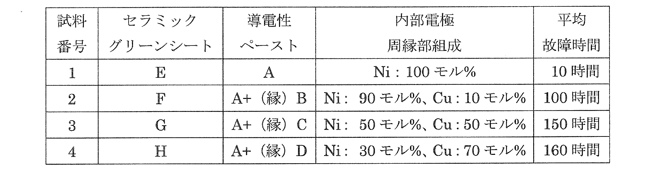
表2において、試料1はこの発明の範囲外の比較例であり、試料2~4がこの発明の範囲内の実施例である。
(6)考察
表2を参照して、試料2~4のように、内部電極周縁部を、NiとCuとの合金化領域、特に、Cu含有比が10モル%以上の合金化領域とすることにより、試料1のNi:100モル%の場合に比べて、平均寿命時間を10~16倍と長くすることができた。
表2を参照して、試料2~4のように、内部電極周縁部を、NiとCuとの合金化領域、特に、Cu含有比が10モル%以上の合金化領域とすることにより、試料1のNi:100モル%の場合に比べて、平均寿命時間を10~16倍と長くすることができた。
なお、以上の実験例は、MとしてCuを用いた場合について実施したものであったが、Cuに代えて、Pt、AuまたはPdを用いた場合であっても同様の効果が得られる。なぜなら、Pt、AuおよびPdは、Cuより少なくとも貴な金属(イオン化傾向が低い金属)であるからである。
1 積層セラミックコンデンサ
2 部品本体
3 セラミック層
4,5 内部電極
6,7 端面
8,9 外部電極
12 主要部
13 周縁部
14 セラミックグリーンシート
15 内部電極パターン
16 Ni膜
17 M膜
2 部品本体
3 セラミック層
4,5 内部電極
6,7 端面
8,9 外部電極
12 主要部
13 周縁部
14 セラミックグリーンシート
15 内部電極パターン
16 Ni膜
17 M膜
Claims (7)
- 積層された複数のセラミック層および前記セラミック層間の界面に沿って配置された内部電極を含み、前記内部電極の端部が所定の面に露出している、部品本体と、
前記部品本体の前記所定の面に露出した前記内部電極の端部に電気的に接続されるように前記部品本体の前記所定の面上に形成された、外部電極と
を備え、
前記内部電極を主要部と周縁部とに区分したとき、前記主要部はNiを主成分とし、前記周縁部の少なくとも一部には、NiとM(Mは、Cu、Pt、AuおよびPdから選ばれる少なくとも1種)とが合金化された合金化領域が形成されている、
積層セラミック電子部品。 - 前記MはCuである、請求項1に記載の積層セラミック電子部品。
- 前記合金化領域には、Cu含有比が10モル%以上の箇所が存在する、請求項2に記載の積層セラミック電子部品。
- 複数のセラミックグリーンシートを用意する工程と、
前記セラミックグリーンシート上に、Niを主成分とするNi膜を形成するとともに、前記Ni膜に接しかつ前記Ni膜の周縁部の少なくとも一部に沿って、少なくともM(Mは、Cu、Pt、AuおよびPdから選ばれる少なくとも1種)を含むM膜を形成することによって、内部電極を形成する工程と、
前記内部電極が形成されたセラミックグリーンシートを含む複数の前記セラミックグリーンシートを積層することによって、生の部品本体を得る工程と、
前記生の部品本体を焼成することによって、前記内部電極の周縁部の少なくとも一部においてNiとMとの合金化を進めるとともに、焼結した部品本体を得る、焼成工程と、
前記部品本体の前記所定の面に露出した前記内部電極の端部に電気的に接続されるように外部電極を形成する工程と
を備える、積層セラミック電子部品の製造方法。 - 前記MとしてCuが選ばれる、請求項1に記載の積層セラミック電子部品の製造方法。
- 前記内部電極を形成する工程において、前記Ni膜は、Ni粉末を含むNi導電性ペーストを塗布することによって形成され、前記M膜は、M粉末を含むM導電性ペーストを塗布することによって形成される、請求項4または5に記載の積層セラミック電子部品の製造方法。
- 前記M導電性ペーストはNi粉末をさらに含み、前記焼成工程において進むNiとMとの合金化に供されるNiの少なくとも一部は、前記M導電性ペースト中のNi粉末によって与えられる、請求項6に記載の積層セラミック電子部品の製造方法。
Applications Claiming Priority (2)
| Application Number | Priority Date | Filing Date | Title |
|---|---|---|---|
| JP2011052828 | 2011-03-10 | ||
| JP2011-052828 | 2011-03-10 |
Publications (1)
| Publication Number | Publication Date |
|---|---|
| WO2012120913A1 true WO2012120913A1 (ja) | 2012-09-13 |
Family
ID=46797884
Family Applications (1)
| Application Number | Title | Priority Date | Filing Date |
|---|---|---|---|
| PCT/JP2012/050053 Ceased WO2012120913A1 (ja) | 2011-03-10 | 2012-01-05 | 積層セラミック電子部品およびその製造方法 |
Country Status (1)
| Country | Link |
|---|---|
| WO (1) | WO2012120913A1 (ja) |
Cited By (2)
| Publication number | Priority date | Publication date | Assignee | Title |
|---|---|---|---|---|
| US20210074476A1 (en) * | 2019-09-09 | 2021-03-11 | Murata Manufacturing Co., Ltd. | Multilayer ceramic electronic component |
| US20230238183A1 (en) * | 2022-01-27 | 2023-07-27 | Murata Manufacturing Co., Ltd. | Three-terminal multilayer ceramic capacitor |
Citations (4)
| Publication number | Priority date | Publication date | Assignee | Title |
|---|---|---|---|---|
| JPH03208323A (ja) * | 1990-01-10 | 1991-09-11 | Murata Mfg Co Ltd | 積層コンデンサ |
| JPH08148372A (ja) * | 1994-11-16 | 1996-06-07 | Taiyo Yuden Co Ltd | 磁器コンデンサ及びその製造方法 |
| JPH10144559A (ja) * | 1996-11-05 | 1998-05-29 | Matsushita Electric Ind Co Ltd | 端子電極ペースト、積層電子部品、およびその製造方法 |
| JP2000049033A (ja) * | 1998-07-27 | 2000-02-18 | Murata Mfg Co Ltd | セラミック電子部品 |
-
2012
- 2012-01-05 WO PCT/JP2012/050053 patent/WO2012120913A1/ja not_active Ceased
Patent Citations (4)
| Publication number | Priority date | Publication date | Assignee | Title |
|---|---|---|---|---|
| JPH03208323A (ja) * | 1990-01-10 | 1991-09-11 | Murata Mfg Co Ltd | 積層コンデンサ |
| JPH08148372A (ja) * | 1994-11-16 | 1996-06-07 | Taiyo Yuden Co Ltd | 磁器コンデンサ及びその製造方法 |
| JPH10144559A (ja) * | 1996-11-05 | 1998-05-29 | Matsushita Electric Ind Co Ltd | 端子電極ペースト、積層電子部品、およびその製造方法 |
| JP2000049033A (ja) * | 1998-07-27 | 2000-02-18 | Murata Mfg Co Ltd | セラミック電子部品 |
Cited By (4)
| Publication number | Priority date | Publication date | Assignee | Title |
|---|---|---|---|---|
| US20210074476A1 (en) * | 2019-09-09 | 2021-03-11 | Murata Manufacturing Co., Ltd. | Multilayer ceramic electronic component |
| US11495404B2 (en) * | 2019-09-09 | 2022-11-08 | Murata Manufacturing Co., Ltd. | Multilayer ceramic electronic component |
| US20230238183A1 (en) * | 2022-01-27 | 2023-07-27 | Murata Manufacturing Co., Ltd. | Three-terminal multilayer ceramic capacitor |
| US12327683B2 (en) * | 2022-01-27 | 2025-06-10 | Murata Manufacturing Co., Ltd. | Three-terminal multilayer ceramic capacitor |
Similar Documents
| Publication | Publication Date | Title |
|---|---|---|
| US9099244B2 (en) | Multilayer ceramic capacitor and method for manufacturing multilayer ceramic capacitor | |
| KR101771728B1 (ko) | 적층 세라믹 전자부품 및 이의 제조방법 | |
| JP5093351B2 (ja) | 積層セラミックコンデンサ | |
| JP4073416B2 (ja) | 積層セラミックコンデンサ | |
| CN104282438A (zh) | 陶瓷电子部件及其制造方法 | |
| US9991054B2 (en) | Multilayer electronic component | |
| JP2015226053A (ja) | 積層セラミックキャパシタ、積層セラミックキャパシタの製造方法、及び積層セラミックキャパシタの実装基板 | |
| JP2005129802A (ja) | 積層セラミックコンデンサ | |
| CN104240950A (zh) | 多层陶瓷电容器和安装有该多层陶瓷电容器的板 | |
| US9997297B2 (en) | Multilayer electronic component | |
| JP5870625B2 (ja) | 電極焼結体、積層電子部品、内部電極ペースト、電極焼結体の製造方法、積層電子部品の製造方法 | |
| JP5772255B2 (ja) | 積層電子部品 | |
| JP2005294314A (ja) | 積層セラミックコンデンサ | |
| JP2019192862A (ja) | 積層セラミックコンデンサおよびその製造方法 | |
| JP2017059815A (ja) | 積層電子部品 | |
| JP5925628B2 (ja) | 積層セラミック電子部品及びその製造方法 | |
| JP4513981B2 (ja) | 積層セラミック電子部品及びその製造方法 | |
| JPWO2011114808A1 (ja) | 積層セラミック電子部品 | |
| WO2022210642A1 (ja) | 積層セラミックコンデンサ | |
| JP5887919B2 (ja) | 電極焼結体および積層電子部品 | |
| WO2012120913A1 (ja) | 積層セラミック電子部品およびその製造方法 | |
| JP2014036218A (ja) | 積層セラミック電子部品及びその製造方法 | |
| JP2009266716A (ja) | 導電性ペーストおよび積層セラミックコンデンサの製造方法 | |
| JP4968309B2 (ja) | ペースト組成物、電子部品および積層セラミックコンデンサの製造方法 | |
| JP5527400B2 (ja) | 積層セラミック電子部品 |
Legal Events
| Date | Code | Title | Description |
|---|---|---|---|
| 121 | Ep: the epo has been informed by wipo that ep was designated in this application |
Ref document number: 12755469 Country of ref document: EP Kind code of ref document: A1 |
|
| NENP | Non-entry into the national phase |
Ref country code: DE |
|
| 122 | Ep: pct application non-entry in european phase |
Ref document number: 12755469 Country of ref document: EP Kind code of ref document: A1 |
|
| NENP | Non-entry into the national phase |
Ref country code: JP |