WO2012114714A1 - 光学部材 - Google Patents
光学部材 Download PDFInfo
- Publication number
- WO2012114714A1 WO2012114714A1 PCT/JP2012/001109 JP2012001109W WO2012114714A1 WO 2012114714 A1 WO2012114714 A1 WO 2012114714A1 JP 2012001109 W JP2012001109 W JP 2012001109W WO 2012114714 A1 WO2012114714 A1 WO 2012114714A1
- Authority
- WO
- WIPO (PCT)
- Prior art keywords
- convex
- lens
- concave portion
- convex portion
- concave
- Prior art date
Links
Images


Classifications
-
- G—PHYSICS
- G02—OPTICS
- G02B—OPTICAL ELEMENTS, SYSTEMS OR APPARATUS
- G02B1/00—Optical elements characterised by the material of which they are made; Optical coatings for optical elements
- G02B1/10—Optical coatings produced by application to, or surface treatment of, optical elements
- G02B1/11—Anti-reflection coatings
- G02B1/118—Anti-reflection coatings having sub-optical wavelength surface structures designed to provide an enhanced transmittance, e.g. moth-eye structures
Definitions
- the technology disclosed herein relates to an optical member.
- the technology disclosed herein relates to an optical member having an antireflection concavo-convex structure that suppresses reflection of incident light on the surface.
- the surface of the optical member has a fine structure (for example, a fine structure composed of regularly arranged linear protrusions or linear concave parts or a regular arrangement with a pitch equal to or less than the wavelength of incident light).
- SWS Subwavelength Structure
- Patent Document 1 discloses an optical element in which a pattern of an antireflection concavo-convex structure is formed so that the depth of a concavo-convex groove is gradually reduced toward the outer periphery.
- the reflection suppressing effect varies depending on the height or depth of the fine structure, the reflection suppressing function may be lowered when the fine structure is lowered.
- the present invention has been made in view of such a point, and an object thereof is to improve a reflection suppressing function in an antireflection structure in which the height or depth of a fine structure varies depending on a region.
- An optical member having at least one curved surface in which a plurality of structural units are regularly arranged, and having an antireflection concavo-convex structure that suppresses reflection of light having a wavelength longer than the period of the structural units,
- the concavo-convex structure has a region where the height of the structural unit is relatively small and a region where the height of the structural unit is relatively large, and the region of the region where the height of the structural unit is relatively small
- An optical member in which substantially flat surfaces are formed on an upper surface and a lower surface of an antireflection concavo-convex structure.
- substantially flat surfaces are formed on the upper and lower surfaces of the antireflection uneven structure in the region where the height of the structural unit is low.
- Light interference can occur at the upper and lower surfaces, which are substantially flat surfaces.
- the antireflection effect in the region where the height of the structural unit is low can be further enhanced.
- FIG. 1 is a cross-sectional view of the lens of the first embodiment.
- FIG. 2 is a partially enlarged view of the antireflection uneven structure of the first embodiment.
- FIG. 3 is a diagram illustrating a process for manufacturing a lens mold.
- FIG. 4 is a graph showing the relationship between the wavelength and the reflectance in the example.
- FIG. 5 is a cross-sectional view of the lens of the second embodiment.
- FIG. 6 is a cross-sectional view of the lens of the third embodiment.
- FIG. 7 is a schematic diagram illustrating a base surface of the first optical surface of the third embodiment.
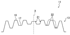
- FIG. 1 shows a cross-sectional view of the lens 11 according to the first embodiment.
- the lens 11 according to Embodiment 1 has an antireflection uneven structure.
- the lens 11 is an example of an optical member.
- the lens 11 has a first optical surface 14, a second optical surface 15, and an edge surface 12.
- the first optical surface 14 and the second optical surface 15 are opposed to each other.
- the edge surface 12 is formed on the outer periphery of the first and second optical surfaces 14 and 15 and is connected to the outer peripheral edges of the first and second optical surfaces 14 and 15.
- SWS antireflection uneven structure
- the SWS 13 has a plurality of convex portions 21 and concave portions 22 arranged alternately to suppress reflection of light having a wavelength longer than the period of the convex portions and concave portions.
- the SWS 13 is configured by regularly arranging a plurality of structural units (convex portions or concave portions), and suppresses reflection of light having a wavelength longer than the period of the structural units.
- the SWS 13 gradually changes the refractive index from the tip of the convex portion 21 toward the bottom of the concave portion 22 and suppresses reflection of light.
- the convex portion 21 is formed in a substantially conical shape.
- the recess 22 is formed in a substantially mortar shape.
- the period of the convex portion 21 or the concave portion 22 is preferably set to be equal to or less than a value obtained by dividing the wavelength of light incident on the lens 11 by the refractive index of the lens 11. Further, the height of the convex portion 21 or the depth of the concave portion 22 is preferably 0.4 times or more the wavelength of light incident on the lens 11. By satisfying these, a sufficient antireflection effect can be exhibited.
- the height of the convex portion 21 is a direction in which the optical axis X of the lens 11 extends from the curved surface passing through the bottom of the concave portion 22 (hereinafter also referred to as a lower base surface) to the top portion of the convex portion 21 (hereinafter referred to as light).
- the depth of the concave portion 22 is a dimension in the optical axis direction from a curved surface passing through the top of the convex portion 21 (hereinafter also referred to as an upper base surface) to the bottom portion of the concave portion 22.
- the period of the convex portion 21 is an interval in the direction parallel to the surface orthogonal to the optical axis X between the top portions of the adjacent convex portions 21.
- the period of the recesses 22 is an interval between the bottoms of the adjacent recesses 22 in a direction parallel to the plane orthogonal to the optical axis X.
- the convex portions 21 and the concave portions 22 are alternately arranged, the height of the convex portions 21 and the depth of the concave portions 22 substantially coincide with each other, and the period of the convex portions 21 and the period of the concave portions 22 substantially coincide with each other.
- the period of the convex part 21 or the concave part 22 is about 266 nm or less, the height of the convex part 21 or If the depth of the recess 22 is about 280 nm or more, a sufficient reflection suppressing effect can be expected.
- the height of the convex portion 21 or the depth of the concave portion 22 is not uniform over the first optical surface 14. That is, the height of the convex portion 21 or the depth of the concave portion 22 varies depending on the location. For example, since a curved surface such as a lens has a different inclination with respect to the optical axis X depending on the location, it is difficult to make the height of the convex portion 21 or the depth of the concave portion 22 uniform when the SWS 13 is formed on the curved surface. is there. In the SWS 13 according to this embodiment, the height of the convex portion 21 is relatively high in the peripheral portion of the first optical surface 14, and the height of the convex portion 21 is relatively low in the central portion of the first optical surface 14.
- the height of the convex portion 21 increases toward the periphery of the first optical surface 14, and the height of the convex portion 21 decreases toward the center of the first optical surface 14.
- the peripheral portion of the first optical surface 14 is an example of a region where the height of the convex portion 21 is relatively small.
- the central portion of the first optical surface 14 is an example of a region where the height of the convex portion 21 is relatively large.
- FIG. 2 is a partial enlarged cross-sectional view of the central portion of the antireflection uneven structure 13 of the lens 11.
- the first flat portion 16 is formed at the top of the convex portion 21, and the second flat portion 17 is formed at the bottom of the concave portion 22.
- the top part of the convex part 21 and the bottom part of the concave part 22 have a sharp shape, and no flat part is formed.
- These first and second flat portions 16 and 17 constitute a flat surface.
- the first and second flat portions 16 and 17 are substantially orthogonal to the optical axis X. That is, the first and second flat portions 16 and 17 are substantially parallel to each other.
- the first and second flat portions 16 and 17 are substantially circular.
- the areas of the first and second flat portions 16 and 17 increase toward the center of the first optical surface 14, that is, as the height of the convex portion 21 decreases and the depth of the concave portion 22 decreases. growing. Note that the first and second flat portions 16 and 17 do not need to be strictly flat, and may be substantially flat.
- the portion of the first flat portion 16 that is farthest from the lower base surface in the optical axis direction is the top of the convex portion 21, and the second The portion of the flat portion 17 that is farthest from the upper base surface in the optical axis direction is the bottom of the concave portion 22, and the lower base surface, the upper base surface, the height of the convex portion 21, the period of the convex portion 21, and the depth of the concave portion 22. Now consider the period of the recess 22.
- the center of the first flat portion 16 is the top of the convex portion 21 and the second flat portion 17
- the center is the top of the recess 22.
- the lower base surface is a curved surface that passes through the bottom of the concave portion 22 that does not have the second flat portion 17 and passes through the center of the second flat portion 17 for the concave portion 22 that has the second flat portion 17.
- the height of the convex portion 21 is a dimension in the optical axis direction from the lower base surface to the center of the first flat portion 16.
- the period of the convex portion 21 is an interval between the centers of the first flat portions 16 of the adjacent convex portions 21 in a direction parallel to the plane orthogonal to the optical axis X.
- the reflection suppressing effect can be improved over the entire surface of the first optical surface 14.
- the convex portion 21 is high and the concave portion 22 is deep. That is, the portion where the convex portion 21 is low or the concave portion 22 is shallow has a smaller reflection suppressing effect than the portion where the convex portion 21 is high or the concave portion 22 is deep.
- the refractive index changes abruptly at the first and second flat portions 16 and 17, and in the first and second flat portions 16 and 17, Part of the incident light is reflected.
- the flat portions are provided in both the convex portion 21 and the concave portion 22, the light reflected by the first flat portion 16 and the light reflected by the second flat portion 15 interfere with each other and weaken each other. As a result, the reflected light as a whole of the first optical surface 14 is suppressed. That is, even if the reflection suppression effect is originally relatively small, the light reflection can be suppressed by using the light interference effect.
- the lens 11 is manufactured by molding using a lens mold.
- the lens mold has an inverted shape of SWS13.
- the lens 11 is molded by, for example, heat press molding.
- the lens 11 is molded by, for example, injection molding or UV molding.
- FIG. 3 shows a process chart for producing the lens mold 37.
- a mold base material 31 is prepared. Then, as shown in FIG. 3A, a lens shape (a state before the SWS 13 is formed) is formed on the mold base material 31 by machining.
- a metal mask 32 is formed on the surface of the mold base material 31 formed in a lens shape.
- a method for forming the metal mask 32 a sputtering method, a vapor deposition method, or the like is preferable.
- a resist mask 33 is formed on the metal mask 32.
- a spin coating method or a spray coating method is preferable.
- a resist dot pattern 34 corresponding to the SWS 13 is formed from the resist mask 33.
- a method for forming the resist dot pattern 34 an electron beam drawing method, an interference exposure (hologram exposure) method, or the like is preferable.
- the hole diameter of the resist dot pattern 34 is preferably uniform over the entire surface.
- the resist dot pattern 34 is transferred to the metal mask 32 by dry etching. Thereby, a metal mask dot pattern 35 is formed.
- the metal mask dot pattern 35 may be formed by wet etching.
- the metal mask dot pattern 35 is transferred to the mold base material 31 by dry etching.
- a lens mold 37 in which the reverse shape 36 of the SWS 13 is formed on the surface of the mold base material 31 is completed.
- plasma (ions) generated in a dry etching apparatus concentrates on the protrusions or corners of the workpiece.
- plasma (ions) tends to concentrate on the end portion 38 of the mold base material 31. Therefore, the etching rate of the end portion 38 where the plasma is concentrated is high, and the etching rate of the central portion is low. As shown in FIG.
- the peripheral portion of the mold base 31 has a high etching speed because the etching rate is high, and the concave portion
- the convex portion is low and the concave portion is shallow.
- the etching time in the central part of the mold base material 31, the height of the convex part at the peripheral part of the mold base material 31 while leaving a flat part at the top part of the convex part and the bottom part of the concave part. And the depth of the recess can be maximized.
- the convex part is high and the concave part is deep in the peripheral part of the lens mold 37, and the convex part is gradually lowered and the concave part is gradually shallower toward the central part. .
- a flat portion is formed at the top of the convex portion at the center of the lens mold 37 and the bottom of the concave portion.
- the lens 11 includes the antireflection concavo-convex structure 13 in which a plurality of convex portions 21 and concave portions 22 are arranged and suppresses reflection of light having a wavelength longer than the period of the convex portions 21 and concave portions 22.
- the antireflection concavo-convex structure 13 includes a region where the convex portion 21 is relatively low and the concave portion 22 is relatively shallow, and a region where the convex portion 21 is relatively high and the concave portion 22 is relatively deep.
- the lens 11 is an optical element having at least one curved surface in which a plurality of structural units are regularly arranged and an antireflection concavo-convex structure that suppresses reflection of light having a wavelength longer than the period of the structural units is formed.
- the antireflection concavo-convex structure is a member having a region where the height of the structural unit is relatively small and a region where the height of the structural unit is relatively large, and the height of the structural unit.
- a substantially flat portion is formed on the upper and lower surfaces of the antireflection concavo-convex structure in a relatively small area.
- the reflection suppressing effect of the convex portion 21 and the concave portion 22 themselves is relatively small.
- the first flat portion 16 is formed at the top of the convex portion 21 and the second flat portion 17 is formed at the bottom of the concave portion 22, so that the reflected light at the first flat portion 16 and the reflected light at the second flat portion 17 are formed.
- the reflection suppression effect can be improved by the interference effect. As a result, even if the configuration is such that the convex portion 21 is relatively low and the concave portion 22 is relatively shallow, and the convex portion 21 is relatively high and the concave portion 22 is relatively deep.
- the suppression effect can be improved as a whole. Further, by making the convex portion 21 low and the concave portion 22 shallow, the antireflection concavo-convex structure 13 can be easily formed. That is, in the region where the ease of making the antireflection concavo-convex structure 13 is required, the first and second flat portions 16, 17 are formed at the top of the convex portion 21 and the bottom of the concave portion 22 by making the convex portion 21 low and the concave portion 22 shallow. By forming the structure, it is possible to prevent the deterioration of the antireflection effect while improving the ease of making the antireflection uneven structure 13. That is, it is possible to achieve both the ease of making the antireflection concavo-convex structure 13 and the antireflection effect, which could not be solved conventionally.
- the first and second flat portions 16 and 17 are larger as the convex portion 21 is lower or the concave portion 22 is shallower.
- the reflection suppressing effect of the convex portion 21 and the concave portion 22 itself becomes smaller.
- the reflection suppressing effect due to interference can be increased by increasing the first flat portion 16 as the convex portion 21 is lowered and increasing the second flat portion 17 as the concave portion 22 is shallow.
- the lens of this example corresponds to the lens 11 of the first embodiment.
- Example> As an example, the following lens was molded.
- Cyclic olefin polymers for example, ZEONEX (registered trademark) (manufactured by ZEON Corporation), ARTON (registered trademark) (manufactured by JSR Corporation), Apel (registered trademark) (manufactured by Mitsui Chemicals, Inc.)
- ZEONEX registered trademark
- ARTON registered trademark
- JSR Corporation manufactured by JSR Corporation
- Apel registered trademark
- silicon carbide (SiC) was prepared as the mold base material 31.
- a lens shape was formed on the die base material 31 by machining, tungsten silicide (WSi) was formed by sputtering, and then an electron beam resist (positive type) was applied by spin coating. Thereafter, a dot shape was drawn by electron beam drawing.
- a dot pattern was formed on the WSi mask by dry etching using argon gas. Thereafter, the SWS inversion shape was formed on the SiC surface of the mold base 31 by dry etching using a fluorocarbon-based gas.
- the lens mold 37 thus fabricated was subjected to a mold release treatment by being immersed in a fluorine-based mold release agent.
- a lens was injection molded using the lens mold 37 subjected to the mold release treatment.
- the lens 11 thus manufactured was a biconvex lens, and had an effective diameter of 16 mm and a lens thickness of 2.4 mm.
- the period of the convex portion 21 and the concave portion 22 was 250 nm over the entire surface of the first optical surface 14.
- the height of the convex portion 21 and the depth of the concave portion 22 are 350 nm at the peripheral portion of the lens and 210 nm at the central portion of the lens 11, and the height gradually decreases toward the central portion.
- first and second flat portions 16 and 17 are formed at the top of the convex portion 21 and the bottom of the concave portion 22 at the center of the lens 11, respectively.
- the outer diameter of the first flat portion 16 at the center of the lens 11 was about 60 nm.
- the areas of the first and second flat portions 16 and 17 became smaller toward the periphery of the lens 11.
- a lens in which the first and second flat portions 16 and 17 were not formed was molded. That is, in the lens according to the comparative example, the first flat portion 16 is not formed in the convex portion 21 in the lens according to the embodiment, and the second flat portion 17 is not formed in the concave portion 22. It was. Therefore, although the period of the convex part 21 and the recessed part 22 is the same in a comparative example and an Example, since the 1st and 2nd flat parts 16 and 17 are not formed, the direction of the comparative example is more convex part 21. High and the recess 22 is deep. Even so, in the lens according to the comparative example, the convex portion 21 is lower and the concave portion 22 is shallower in the central portion than in the peripheral portion. Other than that, the lens of the example and the lens of the comparative example are the same.
- FIG. 4 the result of having measured the reflectance of the lens surface about an Example and a comparative example is shown.
- an optical measuring device USPM-RU III manufactured by Olympus was used for the reflectance.
- BK7 which is a general optical glass
- the reflectance of Examples and Comparative Examples was measured.
- a measurement object (Example or Comparative Example) and a reference were set in the optical measurement apparatus, and the reflectance was measured by irradiating light of 400 to 700 nm.
- the graph of FIG. 7 shows the reflectance with respect to each wavelength of an Example and a comparative example.
- the horizontal axis in FIG. 7 is the wavelength
- the vertical axis is the reflectance.
- Graph (a), (b) is a graph which shows the reflectance of an Example. Specifically, the graph (a) shows a region in which the convex portion 21 is low and the concave portion 22 is shallow in the lens 11 according to the embodiment, and a flat portion is provided at the top of the convex portion 21 and the bottom of the concave portion 22. The reflectance at is shown.
- Graph (b) shows the reflectance in a region where the convex portion 21 is high and the concave portion 22 is deep in the lens 11 according to the example.
- the graph (c) shows the reflectance in the region (center portion of the lens) where the convex portion is low and the concave portion is shallow among the lenses according to the comparative example. In the comparative example, the flat portion is not provided.
- the reflectance with respect to visible light was less than about 1.4%.
- the reflectance with respect to light having a long wavelength among visible light is large.
- the height of the convex portion and the depth of the concave portion are about 210 nm, and the height of the convex portion and the depth of the concave portion for a component having a long wavelength in visible light. Is less than 0.4 times the wavelength. Therefore, the reflection of visible light cannot be sufficiently suppressed.
- the reflectance with respect to visible light is about 0.15% or less.
- a high antireflection effect is exhibited in a region where the convex portion is high and the concave portion is deep, but the antireflection effect is small in a region where the convex portion is low and the concave portion is shallow.
- the reflectance in the example, in the region where the convex portion 21 is high and the concave portion 22 is deep (peripheral portion of the lens), the reflectance can be suppressed to about 0.1% over the entire visible light region. . This is because the height of the convex portion 21 and the depth of the concave portion 22 are about 350 nm, and have a sufficient height and depth with respect to the wavelength of visible light. Further, in the region where the convex portion 21 is low and the concave portion 22 is deep (center portion of the lens), the reflectance can be suppressed to about 0.15% or less over the entire visible light region.
- the interference effect by the 1st flat part 16 of the convex part 21 and the 2nd flat part 17 of the recessed part 22 is exhibited, and the reflection suppression effect by it expressed.
- the effect of suppressing reflection can be made equal between a region where the convex portion 21 is high and the concave portion 22 is deep, and a region where the convex portion 21 is low and the concave portion 22 is shallow.
- a high antireflection effect can be exhibited.
- Embodiment 2 ⁇ Embodiment 2 >> Hereinafter, the second embodiment will be described with reference to the drawings.
- the lens according to the second embodiment is different from the lens according to the first embodiment in the shape of the SWS provided on the optical surface.
- the difference from the first embodiment will be mainly described.
- FIG. 5 is a sectional view of the lens 41.
- the lens 41 has a first optical surface 44, a second optical surface 45, and an edge surface 42.
- a SWS 43 is formed on the first optical surface 44.
- the SWS 43 has a plurality of convex portions 48 and concave portions 49 arranged alternately. In the central portion of the first optical surface 44, the height of the convex portion 48 is relatively high and the depth of the concave portion 49 is relatively large. The height of the convex portion 48 and the depth of the concave portion 49 become lower and shallower toward the peripheral portion of the first optical surface 44.
- a first flat portion 46 is formed at the top of the convex portion 48, and a second flat portion 47 is formed at the bottom of the concave portion 49. Further, the areas of the first and second flat portions 46 and 47 become larger toward the peripheral portion of the first optical surface 44.
- the manufacturing method of the lens 41 is substantially the same as the manufacturing method of the lens 11 according to the first embodiment.
- the resist hole diameter in the peripheral portion is made larger than that in the central portion.
- the dose amount (exposure amount) of electron beam drawing may be changed.
- the first and second flat portions 46 and 47 are formed in the relatively low convex portion 48 and the shallow concave portion 49. That is, in the low convex portion 48 and the shallow concave portion 49, the reflection suppressing effect by the minute concave and convex portion is smaller than that in the high convex portion 48 and the deep concave portion 49, but it can be supplemented by the reflection suppressing effect by the interference effect. As a result, like the first embodiment, the reflectance with respect to visible light on the entire first optical surface 44 can be kept small.
- the peripheral portion of the first optical surface 44 is a portion where the inclination of the first optical surface 44 is the largest, and is a portion that is difficult to release during lens molding.
- a lens having a large inclination angle such as an objective lens capable of condensing blue light
- the amount of glass material deformation during molding increases toward the periphery, and the load on the lens mold increases toward the periphery. Therefore, in the peripheral part, the unevenness of the lens and the unevenness of the lens mold are tightly engaged with each other, making it difficult to release the mold.
- the amount of lens shrinkage in the cooling process during molding increases toward the periphery.
- the unevenness of the lens and the unevenness of the lens mold are closely meshed with each other at the periphery, and it becomes difficult to release the mold.
- the surface area is increased, which makes it more difficult to release.
- the above-mentioned problem is solved by lowering the convex portion 48 and shallowing the concave portion 49 in the peripheral portion and forming the first and second flat portions 46 and 47 in addition thereto. Can be formed easily. That is, it is possible to achieve both the ease of manufacturing the lens and the improvement of the reflection suppression effect.
- Embodiment 3 The third embodiment will be described below with reference to the drawings.
- the lens according to the third embodiment is different from the lenses according to the first and second embodiments in the shape of SWS formed on the optical surface.
- the difference from the first and second embodiments will be mainly described.
- FIG. 6 is a cross-sectional view of the lens 51.
- the lens 51 has a first optical surface 54, a second optical surface 55, and an edge surface 52.
- a SWS 53 is formed on the first optical surface 54.
- the SWS 53 has a plurality of convex portions 58 and concave portions 59 that are alternately arranged.
- the height of the convex portion 58 and the depth of the concave portion 59 are not uniform over the first optical surface 54, and differ depending on the location.
- the height of the convex portion 58 and the depth of the concave portion 59 do not change monotonously according to the radial position of the first optical surface 54, but increase or decrease.
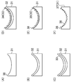
- the first optical surface 54 has a base surface 61 as shown in FIG.
- the base surface 61 has regions A to E.
- Regions A and E are regions located on the outermost periphery of the base surface 61 and are regions having a large inclination angle with respect to the optical axis X (hereinafter simply referred to as “inclination angle”).
- the region C is a region located in the central portion of the base surface 61, and includes a portion where the central inclination angle is gentle and a portion where the peripheral inclination angle is steep.
- the region B is a region located between the region A and the region C, and includes a substantially horizontal portion with a gentle inclination angle.
- the region D is a region located between the region E and the region C, and includes a substantially horizontal portion with a gentle inclination angle.
- the reflection suppressing effect can be improved by the interference effect.
- the reflectance with respect to visible light can be kept small over the entire first optical surface 54.
- regions A and E it is possible to make the structure easy to release during molding without deteriorating the reflection suppressing effect.
- regions B and D the ease of making can be improved without deteriorating the reflection suppression effect.
- regions B and D a high antireflection effect can be exhibited by increasing the convex portion 59 and deepening the concave portion 59. .
- the lens mold for molding such SWS 53 can be manufactured by controlling the hole diameter when forming the resist dot pattern 34 as in the second embodiment.
- the height of the convex portion and the depth of the concave portion are changed in accordance with the lens shape such as the tilt angle and the position of the lens such as the central portion and the peripheral portion.
- molding especially mold release
- the reflection suppressing effect can be improved by providing a flat portion at the top of the convex portion and the bottom of the concave portion. That is, for various reasons, the convex portion may be lowered and the concave portion may be shallow, but even in such a case, it is possible to prevent the reflection suppression effect from deteriorating. As a result, a lens having a high reflection suppression effect can be realized over the entire optical surface.
- the lens manufacturing method and lens mold manufacturing method are not limited to the above-described embodiment.
- the mold base material may be any material that has high strength and is easily finely processed by etching.
- quartz SiO2, silicon carbide (SiC), silicon (Si), glassy carbon (C), carbide (WC), or the like may be used.
- metal mask material Cr, Ta, WSi, Ni, W, etc. may be used.
- the electron beam drawing method is used for manufacturing the lens mold, but the present invention is not limited to this.
- Lithography such as an interference exposure (hologram exposure) method or X-ray lithography may be used.
- the mask may be formed by nanoimprint or particle arrangement.
- the configuration of the lens is not limited to the above embodiment.
- a convex lens has been described, but a concave lens may be used.
- the optical member on which the SWS is formed is not limited to a lens. You may apply SWS of the said structure to the surface of a display, the internal peripheral surface of a lens-barrel, a prism. That is, the base surface on which the SWS 13 is formed may be a flat surface.
- the SWS is provided only on the first optical surface, but is not limited thereto.
- the SWS may be provided on both the first optical surface and the second optical surface, or may be provided only on the second optical surface.
- the convex portion has a conical shape and the concave portion has a mortar shape.
- the convex portion may be a pyramid such as a quadrangular pyramid or a triangular pyramid, and the concave portion may be an inverted shape thereof.
- a convex part and a recessed part are not restricted to a cone shape and its inversion shape, Arbitrary shapes can be employ
- the convex portion may be a linear convex portion extending in the circumferential direction around the optical axis X
- the concave portion may be a linear concave portion extending in the circumferential direction around the optical axis X.
- the flat part formed at the top of the convex part and the bottom part of the concave part has a larger radial width around the optical axis X as the convex part becomes lower and the concave part becomes shallower.
- the optical member according to the present invention has a reflection suppressing effect and high environmental resistance, and is useful as a lens barrel, an optical element represented by a lens, and the like.
- various optical systems such as a high-quality imaging optical system, objective optical system, scanning optical system, and pickup optical system, lens barrel unit, optical pickup unit, and imaging unit
- An optical unit, an imaging device, an optical pickup device, an optical scanning device, and the like can be realized.
Landscapes
- Physics & Mathematics (AREA)
- General Physics & Mathematics (AREA)
- Optics & Photonics (AREA)
- Surface Treatment Of Optical Elements (AREA)
Abstract
レンズ(11)は、複数の凸部(21)及び凹部(22)が配列されてなり、凸部(21)及び凹部(22)の周期以上の波長の光の反射を抑制する反射防止凹凸構造(13)を備えている。反射防止凹凸構造(13)は、凸部(21)が相対的に低く且つ凹部(22)が相対的に浅い領域と、凸部(21)が相対的に高く且つ凹部(22)が相対的に深い領域とを有している。凸部(21)が相対的に低く且つ凹部(22)が相対的に浅い領域においては、凸部(21)の頂部と凹部(22)の底部とに第1及び第2平坦面(16,17)が形成されている。
Description
ここに開示された技術は、光学部材に関する。特に、ここに開示された技術は、入射光の反射を抑制する反射防止凹凸構造が表面に形成された光学部材に関する。
近年、光の反射を抑制する反射防止処理が表面に施された種々の光学部材が提案されている。
反射防止処理の1つとして、光学部材の表面に入射光の波長以下のピッチで微細構造(例えば、規則的に配列された線条凸部又は線条凹部からなる微細構造や、規則的に配列された錐体状若しくは柱状の凸部又はすり鉢状若しくは筒状の凹部からなる微細構造等。以下、このような微細構造が複数配列されてなる構造を「反射防止凹凸構造」又は「SWS(Subwavelength Structure)」と称することがある。)形成する処理が提案されている。
例えば、特許文献1は、反射防止凹凸構造のパターンが外周に向かって徐々に凹凸形状の溝の深さが浅く形成されている光学素子を開示している。
しかし、反射抑制効果は微細構造の高さ又は深さによって異なるため、微細構造が低くなると反射抑制機能も低くなる虞がある。
本発明は、かかる点に鑑みてなされたものであり、その目的とするところは、微細構造の高さ又は深さが領域によって異なる反射防止構造体において、反射抑制機能を向上させることにある。
構造単位が規則的に複数配列されてなり、該構造単位の周期以上の波長の光の反射を抑制する反射防止凹凸構造が形成された少なくともひとつの曲面を有する光学部材であって、前記反射防止凹凸構造は、前記構造単位の高さが相対的に小さい領域と、前記構造単位の高さが相対的に大きい領域と、を有し、前記構造単位の高さが相対的に小さい領域の前記反射防止凹凸構造の上面および下面に略平坦面が形成されている、光学部材。
本発明では、構造単位の高さが低い領域の反射防止凹凸構造の上面および下面に略平坦面が形成されている。略平坦面である上面および下面で光の干渉を起こすことができる。この光の干渉を利用することで、構造単位の高さが低い領域の反射防止効果をより高めることができる。その結果、微細構造の高さが領域によってことなる反射防止構造体において、従来よりも優れた反射防止機能を実現する反射防止構造体を実現することができる。
以下、図面を用いて実施の形態について説明する。
《実施形態1》
[レンズの概要]
図1に、実施形態1に係るレンズ11の断面図を示す。
[レンズの概要]
図1に、実施形態1に係るレンズ11の断面図を示す。
実施形態1に係るレンズ11は、反射防止凹凸構造を有する。レンズ11は、光学部材の一例である。レンズ11は、第1光学面14と、第2光学面15と、コバ面12とを有している。第1光学面14と第2光学面15とは、互いに対向している。コバ面12は、第1及び第2光学面14,15の外周に形成され、第1及び第2光学面14,15の外周縁に接続されている。第1光学面14には、反射防止凹凸構造(以下、SWSと称することがある。)13が形成されている。
SWS13は、複数の凸部21及び凹部22が交互に配列されて、該凸部及び凹部の周期以上の波長の光の反射を抑制する。換言すると、SWS13は、構造単位(凸部又は凹部)が規則的に複数配列されてなり、該構造単位の周期以上の波長の光の反射を抑制する。詳しくは、SWS13は、凸部21の先端から凹部22の底に向かって屈折率を漸次変化させることになり、光の反射を抑制する。凸部21は、略円錐状に形成されている。凹部22は、略すり鉢状に形成されている。凸部21又は凹部22の周期は、レンズ11に入射する光の波長をレンズ11の屈折率で除した値以下に設定されることが好ましい。また、凸部21の高さ又は凹部22の深さは、レンズ11に入射する光の波長の0.4倍以上であることが好ましい。これらを満たすことによって、十分な反射抑制効果を発揮させることができる。ここで、凸部21の高さは、凹部22の底部を通る曲面(以下、下ベース面ともいう)から、凸部21の頂部までの、レンズ11の光軸Xが延びる方向(以下、光軸方向ともいう)の寸法である。凹部22の深さは、凸部21の頂部を通る曲面(以下、上ベース面ともいう)から、凹部22の底部までの光軸方向の寸法である。凸部21の周期は、隣接する凸部21の頂部間の、光軸Xと直交する面と平行な方向への間隔である。凹部22の周期は、隣接する凹部22の底部間の、光軸Xと直交する面と平行な方向への間隔である。凸部21と凹部22とは交互に配列されているので、凸部21の高さと凹部22の深さとは略一致し、凸部21の周期と凹部22の周期とは略一致する。例えば、屈折率1.5のレンズ11に入射する可視光(波長:約400~700nm)の反射を抑制したい場合、凸部21又は凹部22の周期が約266nm以下、凸部21の高さ又は凹部22の深さが約280nm以上であれば、十分な反射抑制効果が期待できる。
ここで、凸部21の高さ又は凹部22の深さは、第1光学面14に亘って均一ではない。すなわち、凸部21の高さ又は凹部22の深さは、場所によって異なる。例えば、レンズなどの曲面は、光軸Xに対する傾きが場所によって異なるので、曲面上にSWS13を形成する場合には、凸部21の高さ又は凹部22の深さを均一にすることが困難である。本実施形態に係るSWS13は、第1光学面14の周辺部では凸部21の高さが相対的に高く、第1光学面14の中心部では凸部21の高さが相対的に低い。詳しくは、SWS13は、第1光学面14の周辺部ほど凸部21の高さが高く、第1光学面14の中心部に向かうにつれて凸部21の高さが低くなっている。第1光学面14の周辺部は、凸部21の高さが相対的に小さい領域の一例である。また、第1光学面14の中心部は、凸部21の高さが相対的に大きい領域の一例である。
[SWSの詳細構造]
図2に、レンズ11の反射防止凹凸構造13の中央部における部分拡大断面図を示す。第1光学面14の中央部においては、凸部21の頂部に第1平坦部16が形成され、凹部22の底部に第2平坦部17が形成されている。第1光学面14の周辺部においては、図1に示すように、凸部21の頂部及び凹部22の底部は、尖鋭な形状をしており、平坦部が形成されていない。これら第1及び第2平坦部16,17が平坦面を構成する。
図2に、レンズ11の反射防止凹凸構造13の中央部における部分拡大断面図を示す。第1光学面14の中央部においては、凸部21の頂部に第1平坦部16が形成され、凹部22の底部に第2平坦部17が形成されている。第1光学面14の周辺部においては、図1に示すように、凸部21の頂部及び凹部22の底部は、尖鋭な形状をしており、平坦部が形成されていない。これら第1及び第2平坦部16,17が平坦面を構成する。
本実施形態では、第1及び第2平坦部16,17は、光軸Xに対して略直交する。すなわち、第1及び第2平坦部16,17は、互いに略平行である。第1及び第2平坦部16,17は、略円形である。また、第1及び第2平坦部16,17の面積は、第1光学面14の中心に向かうにつれて大きく、即ち、凸部21の高さが低くなるにつれて、凹部22の深さが浅くなるにつれて大きくなる。尚、第1及び第2平坦部16,17は、厳密に平坦である必要はなく、実質的に平坦であればよい。
また、第1及び第2平坦部16,17が形成されている場合には、第1平坦部16のうち下ベース面から光軸方向に最も離れた部分を凸部21の頂部とし、第2平坦部17のうち上ベース面から光軸方向に最も離れた部分を凹部22の底部として、前記下ベース面、上ベース面、凸部21の高さ、凸部21の周期、凹部22の深さ、及び凹部22の周期を観念する。本実施形態のように、第1及び第2平坦部16,17が光軸Xに略直交する場合には、第1平坦部16の中心を凸部21の頂部とし、第2平坦部17の中心を凹部22の頂部とする。例えば、下ベース面は、第2平坦部17を有さない凹部22については底部を、第2平坦部17を有する凹部22については、第2平坦部17の中心を通る曲面である。凸部21の高さは、下ベース面から第1平坦部16の中心までの光軸方向の寸法である。凸部21の周期は、隣接する凸部21の第1平坦部16の中心間の、光軸Xと直交する面と平行な方向への間隔である。
このように、第1及び第2平坦部16,17を形成することによって、第1光学面14全面で反射抑制効果を向上させることができる。詳しくは、反射抑制効果の観点からは、凸部21は高く、凹部22は深いことが好ましい。すなわち、凸部21が低い又は凹部22が浅い部分は、凸部21が高い又は凹部22が深い部分に比べて、反射抑制効果が小さい。それに対し、第1及び第2平坦部16,17を設けると、第1及び第2平坦部16,17で屈折率が急激に変化することになり、第1及び第2平坦部16,17では入射した光の一部が反射する。しかしながら、凸部21と凹部22との両方に平坦部が設けられているので、第1平坦部16で反射した光と第2平坦部15で反射した光とは、互いに干渉して弱め合う。その結果、第1光学面14全体としての反射光が抑制される。つまり、本来的には反射抑制効果が相対的に小さい部分であっても、光の干渉効果を利用することによって光の反射を抑制することができる。
[製造方法]
続いて、レンズ11の製造方法について説明する。レンズ11は、レンズ金型を用いた成形により製造する。レンズ金型は、SWS13の反転形状を有している。レンズ11の材料がガラスの場合には、例えば、ヒートプレス成形によりレンズ11が成形される。レンズ11の材料が樹脂の場合には、例えば、射出成形やUV成形によりレンズ11が成形される。
続いて、レンズ11の製造方法について説明する。レンズ11は、レンズ金型を用いた成形により製造する。レンズ金型は、SWS13の反転形状を有している。レンズ11の材料がガラスの場合には、例えば、ヒートプレス成形によりレンズ11が成形される。レンズ11の材料が樹脂の場合には、例えば、射出成形やUV成形によりレンズ11が成形される。
次に、成形に用いるレンズ金型の作製について説明する。図3に、レンズ金型37を作製するための工程図を示す。
まず、金型母材31を用意する。そして、図3(A)に示すように、機械加工により金型母材31にレンズ形状(SWS13が形成される前の状態)を形成する。
次に、図3(B)に示すように、レンズ形状に形成した金型母材31の表面に金属マスク32を形成する。金属マスク32の形成方法としては、スパッタリング法・蒸着法などが好ましい。
次に、図3(C)に示すように、金属マスク32の上にレジストマスク33を形成する。レジストマスク33の形成方法としてはスピンコート法、スプレーコート法が好ましい。
次に、図3(D)に示すように、レジストマスク33から、SWS13に対応したレジストドットパターン34を形成する。レジストドットパターン34の形成方法としては、電子ビーム描画法や干渉露光(ホログラム露光)法などが好ましい。また、レジストドットパターン34の穴径は全面均一であることが好ましい。
次に、図3(E)に示すように、ドライエッチングによりレジストドットパターン34を金属マスク32に転写する。それにより、金属マスクドットパターン35が形成される。なお、金属マスクドットパターン35の形成方法としては、ウェットエッチングでもよい。
次に、図3(F)に示すように、ドライエッチングにより金属マスクドットパターン35を金型母材31に転写する。これにより、金型母材31表面にSWS13の反転形状36が形成されたレンズ金型37が完成する。
一般に、ドライエッチング装置内で発生したプラズマ(イオン)は、被加工材の突起部もしくは角部に集中する。前記プロセスにおいて金型母材31をドライエッチング加工する場合、金型母材31の端部38にプラズマ(イオン)が集中しやすい。そのため、プラズマが集中する端部38のエッチング速度が速く、中央部のエッチング速度が遅くなる。図3(D)で示すように、均一な穴径を有するレジストドットパターン34を用いてドライエッチング加工を行うと、金型母材31の周辺部ではエッチング速度が速いため凸部が高く、凹部が深くなる一方、金型母材31の中央部ではエッチング速度が遅いため凸部が低く、凹部が浅くなる。このとき、エッチング時間を制御することによって、金型母剤31の中央部においては凸部の頂部と凹部の底部に平坦部を残しつつ、金型母材31の周辺部の凸部の高さ及び凹部の深さを最大とすることができる。
このようなプロセスを用いることにより、レンズ金型37の周辺部では凸部が高く且つ凹部が深く、中央部に向かうに従って凸部の高さが徐々に低く且つ凹部の深さが徐々に浅くなる。また、レンズ金型37の中央部の凸部の頂部及び凹部の底部には、平坦部が形成されている。
[効果]
前記実施形態によれば、レンズ11は、複数の凸部21及び凹部22が配列されてなり、該凸部21及び凹部22の周期以上の波長の光の反射を抑制する反射防止凹凸構造13を備えている。前記反射防止凹凸構造13は、前記凸部21が相対的に低く且つ前記凹部22が相対的に浅い領域と、前記凸部21が相対的に高く且つ前記凹部22が相対的に深い領域とを有し、前記凸部21が相対的に低く且つ前記凹部22が相対的に浅い領域においては、前記凸部21の頂部と前記凹部22の底部とにそれぞれ第1及び第2平坦部16,17が形成されている。
前記実施形態によれば、レンズ11は、複数の凸部21及び凹部22が配列されてなり、該凸部21及び凹部22の周期以上の波長の光の反射を抑制する反射防止凹凸構造13を備えている。前記反射防止凹凸構造13は、前記凸部21が相対的に低く且つ前記凹部22が相対的に浅い領域と、前記凸部21が相対的に高く且つ前記凹部22が相対的に深い領域とを有し、前記凸部21が相対的に低く且つ前記凹部22が相対的に浅い領域においては、前記凸部21の頂部と前記凹部22の底部とにそれぞれ第1及び第2平坦部16,17が形成されている。
換言すれば、レンズ11は、構造単位が規則的に複数配列されてなり、該構造単位の周期以上の波長の光の反射を抑制する反射防止凹凸構造が形成された少なくともひとつの曲面を有する光学部材であって、前記反射防止凹凸構造は、前記構造単位の高さが相対的に小さい領域と、前記構造単位の高さが相対的に大きい領域と、を有し、前記構造単位の高さが相対的に小さい領域の前記反射防止凹凸構造の上面及び下面に略平坦部が形成されている。
前記の構成によれば、前記凸部21が相対的に低く且つ前記凹部22が相対的に浅い領域では、凸部21及び凹部22のそれ自体の反射抑制効果は相対的に小さい。しかし、凸部21の頂部に第1平坦部16を形成し、凹部22の底部に第2平坦部17を形成することによって、第1平坦部16における反射光と第2平坦部17における反射光との干渉効果により反射抑制効果を向上させることができる。その結果、凸部21が相対的に低く且つ凹部22が相対的に浅い領域と、凸部21が相対的に高く且つ凹部22が相対的に深い領域とが混在する構成であっても、反射抑制効果を全体的に向上させることができる。また、凸部21を低く且つ凹部22を浅くすることによって、反射防止凹凸構造13を形成し易くすることができる。つまり、反射防止凹凸構造13の作り易さが求められる領域においては凸部21を低く且つ凹部22を浅くし且つ凸部21の頂部及び凹部22の底部に第1及び第2平坦部16,17を形成することによって、反射防止凹凸構造13の作り易さを向上させつつ、反射抑制効果の悪化を防止することができる。つまり、従来は解決できなかった、反射防止凹凸構造13の作り易さと反射抑制効果の両立を図ることができる。
また、前記第1及び第2平坦部16,17は、前記凸部21が低くなるほど、又は、前記凹部22が浅くなるほど、大きくなっている。
つまり、凹部22が浅くなるほど、凸部21及び凹部22のそれ自体の反射抑制効果は小さくなる。それに対して、凸部21が低くなるほど第1平坦部16を大きくし、凹部22が浅くなるほど第2平坦部17を大きくすることによって、干渉による反射抑制効果を大きくすることができる。
以下、実施例について説明する。本実施例のレンズは実施形態1のレンズ11に対応している。
〈実施例〉
実施例として、以下のレンズを成形した。
実施例として、以下のレンズを成形した。
環状オレフィンポリマ(例えば、ZEONEX(登録商標)(日本ゼオン株式会社製)、ARTON(登録商標)(JSR株式会社製)、アペル(登録商標)(三井化学株式会社製)など)をレンズ材料として、レンズ金型を用いて射出成形によってレンズを成形した。
レンズ金型37については、まず、金型母材31としてシリコンカーバイド(SiC)を用意した。機械加工により、金型母材31にレンズ形状を形成し、スパッタリング法によりタングステンシリサイド(WSi)を形成した後、スピンコート法により電子ビーム用レジスト(ポジ型)を塗布した。その後、電子ビーム描画によりドット形状を描画した。
レジストドットパターンをマスクとして、アルゴンガスを用いたドライエッチングによりWSiマスクにドットパターンを形成した。その後、フルオロカーボン系ガスを用いたドライエッチングにより、金型母材31のSiC表面にSWSの反転形状を形成した。
こうして作製されたレンズ金型37を、フッ素系離型剤に浸漬して離型処理した。この離型処理したレンズ金型37を用いて、レンズを射出成形した。
こうして製造されたレンズ11は、両凸レンズであり、その有効径は16mmで、レンズ厚は2.4mmであった。
実施例に用いたレンズ11において、凸部21及び凹部22の周期は、第1光学面14全面に亘って250nmであった。凸部21の高さ及び凹部22の深さは、レンズの周辺部では350nmで、レンズ11の中央部では210nmであり、中央部に向かうにつれて徐々に高さが低くなっていた。また、レンズ11の中央部の凸部21の頂部及び凹部22の底部にはそれぞれ、第1及び第2平坦部16,17が形成されていた。レンズ11の中央における第1平坦部16の外径は、約60nmであった。第1及び第2平坦部16,17の面積は、レンズ11の周辺部に向かうにつれて小さくなっていた。
〈比較例〉
また、比較例として、第1及び第2平坦部16,17が形成されていないレンズを成形した。すなわち、比較例に係るレンズは、実施例に係るレンズにおいて凸部21に第1平坦部16を形成せず、尖鋭な形状とし、凹部22に第2平坦部17を形成せず、尖鋭な形状とした。そのため、比較例と実施例とでは、凸部21及び凹部22の周期は同じであるが、第1及び第2平坦部16,17が形成されていない分、比較例の方が凸部21が高く、凹部22が深い。そうはいっても、比較例に係るレンズにおいては、中央部の方が、周辺部に比べて凸部21が低く、凹部22が浅い。それ以外については、実施例のレンズと比較例のレンズとは同様である。
また、比較例として、第1及び第2平坦部16,17が形成されていないレンズを成形した。すなわち、比較例に係るレンズは、実施例に係るレンズにおいて凸部21に第1平坦部16を形成せず、尖鋭な形状とし、凹部22に第2平坦部17を形成せず、尖鋭な形状とした。そのため、比較例と実施例とでは、凸部21及び凹部22の周期は同じであるが、第1及び第2平坦部16,17が形成されていない分、比較例の方が凸部21が高く、凹部22が深い。そうはいっても、比較例に係るレンズにおいては、中央部の方が、周辺部に比べて凸部21が低く、凹部22が浅い。それ以外については、実施例のレンズと比較例のレンズとは同様である。
〈測定結果〉
図4に、実施例及び比較例について、レンズ表面の反射率を測定した結果を示す。反射率は、オリンパス社製の光学測定装置USPM-RU IIIを用いた。一般的な光学ガラスであるBK7をリファレンスとして、実施例及び比較例の反射率を測定した。具体的には、前記光学測定装置に、測定対象(実施例又は比較例)とリファレンスとをセットし、400~700nmの光を照射し、反射率を測定した。図7のグラフは、実施例及び比較例の各波長に対する反射率を示す。図7の横軸は波長であり、縦軸は反射率である。グラフ(a),(b)は、実施例の反射率を示すグラフである。具体的には、グラフ(a)は、実施例に係るレンズ11のうち凸部21が低く且つ凹部22が浅く、さらには凸部21の頂部及び凹部22の底部に平坦部が設けられた領域での反射率を示している。グラフ(b)は、実施例に係るレンズ11のうち凸部21が高く且つ凹部22が深い領域での反射率を示している。一方、グラフ(c)は、比較例に係るレンズのうちの凸部が低く且つ凹部が浅い領域(レンズの中央部)での反射率を示している。比較例では、平坦部が設けられていない。
図4に、実施例及び比較例について、レンズ表面の反射率を測定した結果を示す。反射率は、オリンパス社製の光学測定装置USPM-RU IIIを用いた。一般的な光学ガラスであるBK7をリファレンスとして、実施例及び比較例の反射率を測定した。具体的には、前記光学測定装置に、測定対象(実施例又は比較例)とリファレンスとをセットし、400~700nmの光を照射し、反射率を測定した。図7のグラフは、実施例及び比較例の各波長に対する反射率を示す。図7の横軸は波長であり、縦軸は反射率である。グラフ(a),(b)は、実施例の反射率を示すグラフである。具体的には、グラフ(a)は、実施例に係るレンズ11のうち凸部21が低く且つ凹部22が浅く、さらには凸部21の頂部及び凹部22の底部に平坦部が設けられた領域での反射率を示している。グラフ(b)は、実施例に係るレンズ11のうち凸部21が高く且つ凹部22が深い領域での反射率を示している。一方、グラフ(c)は、比較例に係るレンズのうちの凸部が低く且つ凹部が浅い領域(レンズの中央部)での反射率を示している。比較例では、平坦部が設けられていない。
比較例については、凸部が低く且つ凹部が浅い領域では、可視光に対する反射率は、約1.4%未満であった。特に、可視光のうち波長が長い光に対する反射率が大きい。凸部が低く且つ凹部が浅い領域では、凸部の高さ及び凹部の深さは約210nmであって、可視光のうち波長が長い成分に対しては凸部の高さ及び凹部の深さが波長の0.4倍未満となっている。そのため、可視光の反射を十分には抑制できていない。尚、図示は省略するが、凸部が高く且つ凹部が深い領域(レンズの周辺部)では、可視光に対する反射率は、約0.15%以下であった。このように、変形例においては、凸部が高く且つ凹部が深い領域においては高い反射抑制効果が発揮されているが、凸部が低く且つ凹部が浅い領域においては反射抑制効果が小さい。
それに対して、実施例については、凸部21が高く且つ凹部22が深い領域(レンズの周辺部)では、可視光域全域に亘って反射率を約0.1%程度に抑えることができた。これは、凸部21の高さ及び凹部22の深さが約350nmであって、可視光の波長に対して十分な高さ及び深さを有しているためである。また、凸部21が低く且つ凹部22が深い領域(レンズの中央部)では、可視光全域に亘って反射率を約0.15%以下に抑えることができた。これは、凸部21の第1平坦部16と凹部22の第2平坦部17とによる干渉効果が発揮され、それによる反射抑制効果が発現したためである。このように、実施例においては、凸部21が低く且つ凹部22が浅い領域の反射抑制効果を向上させることができる。さらには、凸部21が高く且つ凹部22が深い領域と凸部21が低く且つ凹部22が浅い領域とで反射抑制効果を同等にすることができ、ひいては、レンズ11の全面に亘って、均一且つ高い反射抑制効果を発揮させることができる。
《実施形態2》
以下、実施形態2について図面を参照しながら説明する。実施形態2に係るレンズは、光学面上に設けられたSWSの形状が実施形態1のレンズとは異なる。以下、実施形態1との相違点を中心に説明する。
以下、実施形態2について図面を参照しながら説明する。実施形態2に係るレンズは、光学面上に設けられたSWSの形状が実施形態1のレンズとは異なる。以下、実施形態1との相違点を中心に説明する。
図5は、レンズ41の断面図である。レンズ41は、第1光学面44と、第2光学面45と、コバ面42とを有している。第1光学面44には、SWS43が形成されている。SWS43は、交互に配列された複数の凸部48及び凹部49を有している。第1光学面44の中央部では、相対的に、凸部48の高さが高く且つ凹部49の深さが深い。凸部48の高さ及び凹部49の深さは、第1光学面44の周辺部に向かうにつれて低く、浅くなっている。第1光学面44の周辺部においては、凸部48の頂部に第1平坦部46が形成され、凹部49の底部に第2平坦部47が形成されている。また、第1及び第2平坦部46,47の面積は、第1光学面44の周辺部に向かうにつれて大きくなる。
レンズ41の製造方法は、実施形態1に係るレンズ11の製造方法とほぼ同様である。レンズ41用のレンズ金型を作製においては、図3(D)で示したレジストドットパターン34を形成する際に、周辺部のレジスト穴径を中央部に比べて大きくする。レジストドットパターン34の穴径を調整するには、例えば電子ビーム描画のドーズ量(露光量)を変化させればよい。
本実施形態によれば、相対的に低い凸部48及び浅い凹部49に第1及び第2平坦部46,47が形成されている。つまり、低い凸部48及び浅い凹部49では、高い凸部48及び深い凹部49に比べて、微小凹凸部による反射抑制効果が小さいが、干渉効果による反射抑制効果でそれを補うことができる。その結果、実施形態1と同様に、第1光学面44全面での可視光に対する反射率を小さく抑えることができる。
また、第1光学面44の周辺部は、第1光学面44の傾斜が最も大きい部分であり、レンズ成形において離型し難い部分である。例えば、青色光を集光可能な対物レンズのように傾斜角の大きいレンズでは、成形時の硝材変形量が周辺部ほど大きく、レンズ金型への負荷が周辺部ほど大きくなる。そのため、周辺部においては、レンズの凹凸とレンズ金型の凹凸とがきつく噛み合ってしまい、離型し難くなる。また、成形時の冷却工程におけるレンズの収縮量は、周辺部ほど大きくなる。この点においても、レンズの凹凸とレンズ金型の凹凸とが周辺部できつく噛み合ってしまい、離型し難くなる。特に、SWS43のような微細構造を有する構成においては表面積が増大するため、さらに離型し難くなる。それに対し、本実施形態では、周辺部における凸部48を低くし且つ凹部49を浅くし、それに加えて、第1及び第2平坦部46,47を形成することによって、前述の問題を解決することができ、成形を容易にすることができる。つまり、レンズの作り易さと反射抑制効果の向上の両立を図ることができる。
《実施形態3》
以下、実施形態3について図面を参照しながら説明する。実施形態3に係るレンズは、光学面上に形成されたSWSの形状が、実施形態1,2のレンズと異なる。以下、実施形態1,2との相違点を中心に説明する。
以下、実施形態3について図面を参照しながら説明する。実施形態3に係るレンズは、光学面上に形成されたSWSの形状が、実施形態1,2のレンズと異なる。以下、実施形態1,2との相違点を中心に説明する。
図6は、レンズ51の断面図である。レンズ51は、第1光学面54と、第2光学面55と、コバ面52とを有している。第1光学面54には、SWS53が形成されている。SWS53は、交互に配列された複数の凸部58及び凹部59を有している。SWS53は、凸部58の高さ及び凹部59の深さが第1光学面54に亘って均一ではなく、場所によって異なっている。さらに、凸部58の高さ及び凹部59の深さは、第1光学面54の半径方向位置に応じて単調に変化するのではなく、増加したり減少したりする。
詳しくは、第1光学面54は、図7に示すようなベース面61を有している。ベース面61は、領域A~Eを有している。領域A,Eは、ベース面61の最も周辺に位置する領域であり、光軸Xに対する傾斜角(以下、単に「傾斜角」という)が大きい領域である。領域Cは、ベース面61の中央部に位置する領域であり、中央の傾斜角が緩やかな部分と、その周辺の傾斜角が急な部分とを含んでいる。領域Bは、領域Aと領域Cとの間に位置する領域であり、傾斜角が緩やかで略水平な部分を含んでいる。領域Dは、領域Eと領域Cとの間に位置する領域であり、傾斜角が緩やかで略水平な部分を含んでいる。
領域A,Eでは、傾斜角が大きいので、凸部58を低く且つ凹部59を浅くしている。領域B,Dでは、傾斜角が小さいので、凸部58を高く且つ凹部59を深くしている。領域Cでは、傾斜角は小さいものの、金型の作り易さ及びレンズ成形のし易さを優先して、凸部58を低く且つ凹部59を浅くしている。そして、凸部58が低く且つ凹部59が浅い領域A,C,Eにおいては、凸部58の頂部に第1平坦部56が形成され、凹部59の底部に第2平坦部57が形成されている。
これにより、凸部58が低く且つ凹部59が浅い領域であっても、干渉効果により反射抑制効果を向上させることができる。その結果、実施形態1,2と同様に、第1光学面54全面で可視光に対する反射率を小さく抑えることができる。また、領域A,Eのように傾斜角が大きい領域においても、反射抑制効果を悪化させることなく、成形時に離型し易い構造とすることができる。また、領域Cのように、傾斜角にかかわらず、SWS13の作り易さを向上させたい領域においても、反射抑制効果を悪化させることなく、作り易さを向上させることができる。さらに、領域B,Dのように、SWS13の高さ及び深さを小さくする必要がない領域においては、凸部59を高く、凹部59を深くすることによって高い反射抑制効果を発揮させることができる。
尚、このようなSWS53を成形するためのレンズ金型は、実施形態2と同様に、レジストドットパターン34を形成する際の穴径を制御することにより作製できる。
以上、実施形態1~3で説明したとおり、傾斜角などのレンズ形状や、中央部や周辺部などのレンズの位置に応じて、凸部の高さ及び凹部の深さを変化させている。これにより、金型作製及び成形(特に、離型)を容易にすることができる。それに加えて、相対的に凸部が低く且つ凹部が浅い領域においては、凸部の頂部及び凹部の底部に平坦部を設けることによって、反射抑制効果を向上させることができる。つまり、種々の理由により凸部を低く且つ凹部を浅くする場合があるが、そのような場合であっても反射抑制効果の悪化を防止することができる。その結果、光学面全面で反射抑制効果の高いレンズを実現できる。
《その他の実施形態》
前記実施形態について、以下のような構成としてもよい。
前記実施形態について、以下のような構成としてもよい。
レンズの製造方法及びレンズ金型の作製方法は、前記実施形態に限られるものではない。
例えば、金型母材は、高強度で且つエッチングにより微細加工し易い材料であればよい。例えば、石英SiO2、シリコンカーバイド(SiC)、シリコン(Si)、グラッシーカーボン(C)、超硬(WC)などでもよい。
金属マスク材料としては、Cr、Ta、WSi、Ni、Wなどでもよい。
前記実施形態では、レンズ金型の作製に電子ビーム描画法を用いたが、これに限られるものではない。干渉露光(ホログラム露光)法、X線リソグラフィなどのリソグラフィでもよい。また、ナノインプリントや粒子配列によってマスクを形成してもよい。
レンズ金型を用いてレンズ成形を行う場合は、成形前に金型の成形面を離型処理したほうがよい。ガラス成形であれば、カーボン、窒化硼素、DLC、貴金属膜(白金(Pt)、パラジウム(Pd)、イリジウム(Ir)、ロジウム(Rh)、オスミウム(Os)、ルテニウム(Ru)、レニウム(Re)、タングステン(W)、タンタル(Ta)のうち、少なくとも1種類以上の金属を含む合金)などの薄膜を表面に形成すればよい。樹脂成形であれば、フッ素系離型剤を成形面に塗布すればよい。このような離型処理を行うことで、成形品の離型性を高めることができる。
また、レンズの構成は、前記実施形態に限られるものではない。
例えば、前記実施形態では、凸レンズについて説明したが、凹レンズであってもよい。
さらには、SWSが形成される光学部材は、レンズに限られるものではない。ディスプレイの表面、鏡筒の内周面、プリズム等に前記構成のSWSを適用してもよい。すなわち、SWS13が形成されるベース面は、平面であってもよい。
前記実施形態では、SWSは第1光学面上にのみ設けられているが、これに限られない。SWSは、第1光学面と第2光学面の両方に設けられてもよいし、第2光学面のみに設けられてもよい。
前記実施形態では、凸部は円錐状であり、凹部はすり鉢状であるが、これに限られるものではない。例えば、凸部は、四角錘や三角錐等の角錐であってもよく、凹部は、それらの反転形状であってもよい。また、凸部及び凹部は、錐体状及びその反転形状に限られるものではなく、任意の形状を採用することができる。また、凸部は、光軸X周りの周方向に延びる線条凸部であってもよく、凹部は、光軸X周りの周方向に延びる線条凹部であってもよい。その場合、凸部の頂部及び凹部の底部に形成される平坦部は、凸部が低くなるにつれて、凹部が浅くなるにつれて、光軸Xを中心とする半径方向の幅が大きくなる。
本発明は、前記実施形態に限定されず、その精神または主要な特徴から逸脱することなく他のいろいろな形で実施することができる。このように、上述の実施形態はあらゆる点で単なる例示に過ぎず、限定的に解釈してはならない。本発明の範囲は請求の範囲によって示すものであって、明細書本文には何ら拘束されない。さらに、請求の範囲の均等範囲に属する変形や変更は、すべて本発明の範囲内のものである。
本発明に係る光学部材は、反射抑制効果及び高い耐環境性を有し、レンズ鏡筒や、レンズ等に代表される光学素子等として有用である。本発明に係る光学部材を用いることによって、高品位な結像光学系、対物光学系、走査光学系、ピックアップ光学系等の各種光学系、レンズ鏡筒ユニット、光ピックアップユニット、撮像ユニット等の各種光学ユニット、及び撮像装置、光ピックアップ装置、光走査装置等を実現することが可能となる。
11、41、51 レンズ
12 コバ面
13、43、53 反射防止凹凸構造
14、44、54 第1光学面
15、45、55 第2光学面
16、46、56 第1平坦部(平坦面)
17、47、57 第2平坦部(平坦面)
21、48、58 凸部
22、49、59 凹部
31 金型母材
32 金属マスク
33 レジストマスク
34 レジストドットパターン
35 金属マスクドットパターン
36 反転形状
37 レンズ金型
12 コバ面
13、43、53 反射防止凹凸構造
14、44、54 第1光学面
15、45、55 第2光学面
16、46、56 第1平坦部(平坦面)
17、47、57 第2平坦部(平坦面)
21、48、58 凸部
22、49、59 凹部
31 金型母材
32 金属マスク
33 レジストマスク
34 レジストドットパターン
35 金属マスクドットパターン
36 反転形状
37 レンズ金型
Claims (7)
- 複数の凸部及び凹部が配列されてなり、該凸部及び凹部の周期以上の波長の光の反射を抑制する反射防止凹凸構造を備えた光学部材であって、
前記反射防止凹凸構造は、前記凸部が相対的に低く且つ前記凹部が相対的に浅い領域と、前記凸部が相対的に高く且つ前記凹部が相対的に深い領域とを有し、
前記凸部が相対的に低く且つ前記凹部が相対的に浅い領域においては、前記凸部の頂部と前記凹部の底部とに平坦面が形成されている光学部材。 - 前記平坦面は、前記凸部が低くなるほど、又は、前記凹部が浅くなるほど、大きくなる、請求項1に記載の光学部材。
- 前記反射防止凹凸構造は、曲面上に形成されており、
前記曲面は、中央部に比べて周辺部の傾斜が急な形状であり、
前記曲面の中央部よりも前記曲面の周辺部の方が、前記凸部が低く且つ前記凹部が浅い、請求項1に記載の光学部材。 - 前記凸部は、前記曲面の中央部から前記曲面の周辺部に向かって低くなり、
前記凹部は、前記曲面の中央部から前記曲面の周辺部に向かって浅くなる、請求項3に記載の光学部材。 - 前記反射防止構造は、中央部に比べて周辺部の傾斜が急な曲面上に形成されており、
前記曲面の周辺部よりも前記曲面の中央部の方が、前記凸部が低く且つ前記凹部が浅い、請求項1に記載の光学部材。 - 前記凸部は、前記曲面の周辺部から前記曲面の中央部に向かって低くなり、
前記凹部は、前記曲面の周辺部から前記曲面の中央部に向かって浅くなる、請求項5に記載の光学部材。 - 前記凸部が相対的に低く且つ前記凹部が相対的に浅い領域と、前記凸部が相対的に高く且つ前記凹部が相対的に深い領域とが、交互に並んで形成されている、請求項1に記載の光学部材。
Priority Applications (2)
| Application Number | Priority Date | Filing Date | Title |
|---|---|---|---|
| JP2012527925A JP5352010B2 (ja) | 2011-02-22 | 2012-02-20 | 光学部材 |
| US13/765,111 US9268067B2 (en) | 2011-02-22 | 2013-02-12 | Optical component having antireflection structure |
Applications Claiming Priority (2)
| Application Number | Priority Date | Filing Date | Title |
|---|---|---|---|
| JP2011-035663 | 2011-02-22 | ||
| JP2011035663 | 2011-02-22 |
Related Child Applications (1)
| Application Number | Title | Priority Date | Filing Date |
|---|---|---|---|
| US13/765,111 Continuation US9268067B2 (en) | 2011-02-22 | 2013-02-12 | Optical component having antireflection structure |
Publications (1)
| Publication Number | Publication Date |
|---|---|
| WO2012114714A1 true WO2012114714A1 (ja) | 2012-08-30 |
Family
ID=46720508
Family Applications (1)
| Application Number | Title | Priority Date | Filing Date |
|---|---|---|---|
| PCT/JP2012/001109 WO2012114714A1 (ja) | 2011-02-22 | 2012-02-20 | 光学部材 |
Country Status (3)
| Country | Link |
|---|---|
| US (1) | US9268067B2 (ja) |
| JP (1) | JP5352010B2 (ja) |
| WO (1) | WO2012114714A1 (ja) |
Cited By (9)
| Publication number | Priority date | Publication date | Assignee | Title |
|---|---|---|---|---|
| WO2013150744A1 (ja) * | 2012-04-04 | 2013-10-10 | パナソニック株式会社 | 光学素子、それを備えた撮像装置及び光学素子の製造方法 |
| WO2013150742A1 (ja) * | 2012-04-04 | 2013-10-10 | パナソニック株式会社 | 光学素子、それを備えた撮像装置及び光学素子の製造方法 |
| JP2014102311A (ja) * | 2012-11-19 | 2014-06-05 | Seiko Epson Corp | マイクロレンズアレイ基板、マイクロレンズアレイ基板の製造方法、電気光学装置、電子機器 |
| WO2014112593A1 (ja) * | 2013-01-17 | 2014-07-24 | コニカミノルタ株式会社 | 光学素子の製造方法及び反射防止構造体の作製方法 |
| JP2018527629A (ja) * | 2015-08-14 | 2018-09-20 | マツクス−プランク−ゲゼルシヤフト ツール フエルデルング デル ヴイツセンシヤフテン エー フアウMAX−PLANCK−GESELLSCHAFT ZUR FOeRDERUNG DER WISSENSCHAFTEN E.V. | 単一基板上に複数のナノ構造勾配を含むナノ構造基板の製造 |
| JP2019204051A (ja) * | 2018-05-25 | 2019-11-28 | 国立研究開発法人産業技術総合研究所 | 光接続部品、及び光接続部品の製造方法 |
| JP2020521530A (ja) * | 2017-06-01 | 2020-07-27 | カール・ツアイス・メディテック・アーゲー | 回折格子構造を有する人工水晶体及び人工水晶体を製造する方法 |
| US11583391B2 (en) | 2017-06-01 | 2023-02-21 | Carl Zeiss Meditec Ag | Artificial eye lens with laser-generated birefringent structure and method for producing an artificial eye lens |
| WO2023189459A1 (ja) * | 2022-03-28 | 2023-10-05 | ソニーセミコンダクタソリューションズ株式会社 | 光検出装置およびその製造方法、並びに電子機器 |
Families Citing this family (2)
| Publication number | Priority date | Publication date | Assignee | Title |
|---|---|---|---|---|
| JP2015220313A (ja) | 2014-05-16 | 2015-12-07 | ソニー株式会社 | 固体撮像装置およびその製造方法、並びに電子機器 |
| KR101746076B1 (ko) | 2015-04-20 | 2017-06-12 | 주식회사 이엘피 | 미세 형상 구조체를 갖는 렌즈 및 그 렌즈 제조 방법 |
Citations (3)
| Publication number | Priority date | Publication date | Assignee | Title |
|---|---|---|---|---|
| JP2005157325A (ja) * | 2003-10-27 | 2005-06-16 | Matsushita Electric Ind Co Ltd | 光量分布制御素子、並びにそれを用いた光学機器 |
| WO2007018149A1 (ja) * | 2005-08-08 | 2007-02-15 | Matsushita Electric Industrial Co., Ltd. | 撮像光学系 |
| JP2007127855A (ja) * | 2005-11-04 | 2007-05-24 | Konica Minolta Holdings Inc | 光学素子 |
Family Cites Families (10)
| Publication number | Priority date | Publication date | Assignee | Title |
|---|---|---|---|---|
| JP2002267815A (ja) | 2001-03-08 | 2002-09-18 | Dainippon Printing Co Ltd | 反射防止性成形品およびその製造方法 |
| US7239448B2 (en) | 2003-10-27 | 2007-07-03 | Matsushita Electric Industrial Co., Ltd | Light quantity distribution control element and optical apparatus using the same |
| US20070144700A1 (en) * | 2004-03-25 | 2007-06-28 | Sanyo Electric Co., Ltd. | Production method of curved-surface metal mold having fine uneven structure and production method of optical element using this metal mold |
| JP2005283814A (ja) * | 2004-03-29 | 2005-10-13 | Sanyo Electric Co Ltd | 反射防止処理を施した光学素子及びその金型並びに金型の製造方法 |
| US20100172027A1 (en) | 2006-06-06 | 2010-07-08 | Kazuhiro Yamada | Optical member |
| US20100271706A1 (en) | 2006-06-21 | 2010-10-28 | Panasonic Corporation | Optical member and optical system, optical unit and optical device including the optical member |
| WO2008001662A1 (fr) * | 2006-06-30 | 2008-01-03 | Panasonic Corporation | Élément optique et dispositif optique le comprenant |
| JP4933173B2 (ja) | 2006-07-03 | 2012-05-16 | 株式会社リコー | 成形品、成形型、光学素子、光学装置、光走査装置、画像表示装置、光ピックアップ装置 |
| JP4539657B2 (ja) * | 2007-01-18 | 2010-09-08 | ソニー株式会社 | 反射防止用光学素子 |
| JP2009198628A (ja) | 2008-02-20 | 2009-09-03 | Nissan Motor Co Ltd | 反射防止構造及び反射防止成形体 |
-
2012
- 2012-02-20 WO PCT/JP2012/001109 patent/WO2012114714A1/ja active Application Filing
- 2012-02-20 JP JP2012527925A patent/JP5352010B2/ja not_active Expired - Fee Related
-
2013
- 2013-02-12 US US13/765,111 patent/US9268067B2/en not_active Expired - Fee Related
Patent Citations (3)
| Publication number | Priority date | Publication date | Assignee | Title |
|---|---|---|---|---|
| JP2005157325A (ja) * | 2003-10-27 | 2005-06-16 | Matsushita Electric Ind Co Ltd | 光量分布制御素子、並びにそれを用いた光学機器 |
| WO2007018149A1 (ja) * | 2005-08-08 | 2007-02-15 | Matsushita Electric Industrial Co., Ltd. | 撮像光学系 |
| JP2007127855A (ja) * | 2005-11-04 | 2007-05-24 | Konica Minolta Holdings Inc | 光学素子 |
Cited By (16)
| Publication number | Priority date | Publication date | Assignee | Title |
|---|---|---|---|---|
| US9285509B2 (en) | 2012-04-04 | 2016-03-15 | Panasonic Intellectual Property Management Co., Ltd. | Optical element, imaging apparatus including the element, and method of manufacturing the optical element |
| WO2013150742A1 (ja) * | 2012-04-04 | 2013-10-10 | パナソニック株式会社 | 光学素子、それを備えた撮像装置及び光学素子の製造方法 |
| JP5555816B2 (ja) * | 2012-04-04 | 2014-07-23 | パナソニック株式会社 | 光学素子、それを備えた撮像装置及び光学素子の製造方法 |
| JP5555817B2 (ja) * | 2012-04-04 | 2014-07-23 | パナソニック株式会社 | 光学素子、それを備えた撮像装置及び光学素子の製造方法 |
| WO2013150744A1 (ja) * | 2012-04-04 | 2013-10-10 | パナソニック株式会社 | 光学素子、それを備えた撮像装置及び光学素子の製造方法 |
| US9279916B2 (en) | 2012-04-04 | 2016-03-08 | Panasonic Intellectual Property Management Co., Ltd. | Optical element, imaging apparatus including the element, and method of manufacturing the optical element |
| JP2014102311A (ja) * | 2012-11-19 | 2014-06-05 | Seiko Epson Corp | マイクロレンズアレイ基板、マイクロレンズアレイ基板の製造方法、電気光学装置、電子機器 |
| JPWO2014112593A1 (ja) * | 2013-01-17 | 2017-01-19 | コニカミノルタ株式会社 | 光学素子の製造方法及び反射防止構造体の作製方法 |
| WO2014112593A1 (ja) * | 2013-01-17 | 2014-07-24 | コニカミノルタ株式会社 | 光学素子の製造方法及び反射防止構造体の作製方法 |
| JP2018527629A (ja) * | 2015-08-14 | 2018-09-20 | マツクス−プランク−ゲゼルシヤフト ツール フエルデルング デル ヴイツセンシヤフテン エー フアウMAX−PLANCK−GESELLSCHAFT ZUR FOeRDERUNG DER WISSENSCHAFTEN E.V. | 単一基板上に複数のナノ構造勾配を含むナノ構造基板の製造 |
| JP2020521530A (ja) * | 2017-06-01 | 2020-07-27 | カール・ツアイス・メディテック・アーゲー | 回折格子構造を有する人工水晶体及び人工水晶体を製造する方法 |
| JP7152421B2 (ja) | 2017-06-01 | 2022-10-12 | カール・ツアイス・メディテック・アーゲー | 回折格子構造を有する人工水晶体及び人工水晶体を製造する方法 |
| US11583391B2 (en) | 2017-06-01 | 2023-02-21 | Carl Zeiss Meditec Ag | Artificial eye lens with laser-generated birefringent structure and method for producing an artificial eye lens |
| JP2019204051A (ja) * | 2018-05-25 | 2019-11-28 | 国立研究開発法人産業技術総合研究所 | 光接続部品、及び光接続部品の製造方法 |
| JP7258327B2 (ja) | 2018-05-25 | 2023-04-17 | 国立研究開発法人産業技術総合研究所 | 光接続部品、及び光接続部品の製造方法 |
| WO2023189459A1 (ja) * | 2022-03-28 | 2023-10-05 | ソニーセミコンダクタソリューションズ株式会社 | 光検出装置およびその製造方法、並びに電子機器 |
Also Published As
| Publication number | Publication date |
|---|---|
| US9268067B2 (en) | 2016-02-23 |
| JP5352010B2 (ja) | 2013-11-27 |
| US20130148206A1 (en) | 2013-06-13 |
| JPWO2012114714A1 (ja) | 2014-07-07 |
Similar Documents
| Publication | Publication Date | Title |
|---|---|---|
| JP5352010B2 (ja) | 光学部材 | |
| JP5587672B2 (ja) | マスクブランク用基板の製造方法、インプリントモールド用マスクブランクの製造方法、及びインプリントモールドの製造方法 | |
| US8328371B2 (en) | Anti-reflection structure body, method of producing the same and method of producing optical member | |
| JP6470176B2 (ja) | 多層反射膜付き基板、euvリソグラフィー用反射型マスクブランク、euvリソグラフィー用反射型マスク及びその製造方法、並びに半導体装置の製造方法 | |
| JP4916597B2 (ja) | 型および型の製造方法ならびに反射防止膜 | |
| JP5521655B2 (ja) | 反射型スクリーン、投影システム、フロントプロジェクションテレビ及び反射型スクリーンの製造方法 | |
| JPWO2005109042A1 (ja) | 光学素子及びその製造方法 | |
| JP5615971B2 (ja) | 型の製造方法 | |
| JP4739729B2 (ja) | 反射防止構造体を備えた部材の製造方法 | |
| JP6458051B2 (ja) | 型および型の製造方法ならびに反射防止膜 | |
| JP5525656B2 (ja) | 光学素子の製造方法 | |
| US20120062995A1 (en) | Optical element with antireflection function and optical apparatus including the same | |
| JPWO2016031167A1 (ja) | 反射防止膜および反射防止膜を備えた光学部材 | |
| JP4714627B2 (ja) | 表面に微細な凹凸構造を有する構造体の製造方法 | |
| TW202143330A (zh) | 平坦化設備、平坦化程序及製造物品的方法 | |
| JP2005132679A (ja) | 無反射構造を有する光学素子の製造方法、及び当該方法により製造された無反射構造を有する光学素子 | |
| WO2020031945A1 (ja) | 反射防止構造体付き光学素子、その製造方法、製造用金型の製造方法及び撮像装置 | |
| JP5414945B1 (ja) | 光学素子及びそれを備えた撮像装置 | |
| JP5622118B2 (ja) | 反射防止フィルム、反射防止フィルムの作製に用いられる型、および、型の製造方法 | |
| JP2016004096A (ja) | 光学素子及びそれを備えた撮像装置 | |
| JP7192409B2 (ja) | インプリントモールド用基板及びインプリントモールド、並びにそれらの製造方法 | |
| KR20130068549A (ko) | 비반사 유리 및 그 제조방법 | |
| JP5935281B2 (ja) | 型、型の製造方法、および、型を用いた反射防止フィルムの製造方法 | |
| JP7346547B2 (ja) | 表面微細構造を備えた基体 | |
| JP2023039111A (ja) | 回折光学素子、その製造方法および型の製造方法 |
Legal Events
| Date | Code | Title | Description |
|---|---|---|---|
| WWE | Wipo information: entry into national phase |
Ref document number: 2012527925 Country of ref document: JP |
|
| 121 | Ep: the epo has been informed by wipo that ep was designated in this application |
Ref document number: 12749102 Country of ref document: EP Kind code of ref document: A1 |
|
| NENP | Non-entry into the national phase |
Ref country code: DE |
|
| 122 | Ep: pct application non-entry in european phase |
Ref document number: 12749102 Country of ref document: EP Kind code of ref document: A1 |