WO2012111821A1 - A/d変換器、イメージセンサデバイス及びアナログ信号からディジタル信号を生成する方法 - Google Patents
A/d変換器、イメージセンサデバイス及びアナログ信号からディジタル信号を生成する方法 Download PDFInfo
- Publication number
- WO2012111821A1 WO2012111821A1 PCT/JP2012/053868 JP2012053868W WO2012111821A1 WO 2012111821 A1 WO2012111821 A1 WO 2012111821A1 JP 2012053868 W JP2012053868 W JP 2012053868W WO 2012111821 A1 WO2012111821 A1 WO 2012111821A1
- Authority
- WO
- WIPO (PCT)
- Prior art keywords
- conversion
- reference voltage
- output
- input
- signal
- Prior art date
- Legal status (The legal status is an assumption and is not a legal conclusion. Google has not performed a legal analysis and makes no representation as to the accuracy of the status listed.)
- Ceased
Links
Images






Classifications
-
- H—ELECTRICITY
- H03—ELECTRONIC CIRCUITRY
- H03M—CODING; DECODING; CODE CONVERSION IN GENERAL
- H03M1/00—Analogue/digital conversion; Digital/analogue conversion
- H03M1/12—Analogue/digital converters
- H03M1/18—Automatic control for modifying the range of signals the converter can handle, e.g. gain ranging
-
- H—ELECTRICITY
- H03—ELECTRONIC CIRCUITRY
- H03M—CODING; DECODING; CODE CONVERSION IN GENERAL
- H03M1/00—Analogue/digital conversion; Digital/analogue conversion
- H03M1/12—Analogue/digital converters
- H03M1/14—Conversion in steps with each step involving the same or a different conversion means and delivering more than one bit
-
- H—ELECTRICITY
- H03—ELECTRONIC CIRCUITRY
- H03M—CODING; DECODING; CODE CONVERSION IN GENERAL
- H03M1/00—Analogue/digital conversion; Digital/analogue conversion
- H03M1/12—Analogue/digital converters
- H03M1/14—Conversion in steps with each step involving the same or a different conversion means and delivering more than one bit
- H03M1/16—Conversion in steps with each step involving the same or a different conversion means and delivering more than one bit with scale factor modification, i.e. by changing the amplification between the steps
- H03M1/162—Conversion in steps with each step involving the same or a different conversion means and delivering more than one bit with scale factor modification, i.e. by changing the amplification between the steps the steps being performed sequentially in a single stage, i.e. recirculation type
-
- H—ELECTRICITY
- H03—ELECTRONIC CIRCUITRY
- H03M—CODING; DECODING; CODE CONVERSION IN GENERAL
- H03M3/00—Conversion of analogue values to or from differential modulation
- H03M3/30—Delta-sigma modulation
- H03M3/39—Structural details of delta-sigma modulators, e.g. incremental delta-sigma modulators
-
- H—ELECTRICITY
- H03—ELECTRONIC CIRCUITRY
- H03M—CODING; DECODING; CODE CONVERSION IN GENERAL
- H03M3/00—Conversion of analogue values to or from differential modulation
- H03M3/30—Delta-sigma modulation
- H03M3/458—Analogue/digital converters using delta-sigma modulation as an intermediate step
- H03M3/46—Analogue/digital converters using delta-sigma modulation as an intermediate step using a combination of at least one delta-sigma modulator in series with at least one analogue/digital converter of a different type
-
- H—ELECTRICITY
- H04—ELECTRIC COMMUNICATION TECHNIQUE
- H04N—PICTORIAL COMMUNICATION, e.g. TELEVISION
- H04N25/00—Circuitry of solid-state image sensors [SSIS]; Control thereof
- H04N25/70—SSIS architectures; Circuits associated therewith
- H04N25/76—Addressed sensors, e.g. MOS or CMOS sensors
- H04N25/77—Pixel circuitry, e.g. memories, A/D converters, pixel amplifiers, shared circuits or shared components
-
- H—ELECTRICITY
- H03—ELECTRONIC CIRCUITRY
- H03M—CODING; DECODING; CODE CONVERSION IN GENERAL
- H03M1/00—Analogue/digital conversion; Digital/analogue conversion
- H03M1/12—Analogue/digital converters
- H03M1/34—Analogue value compared with reference values
- H03M1/38—Analogue value compared with reference values sequentially only, e.g. successive approximation type
- H03M1/40—Analogue value compared with reference values sequentially only, e.g. successive approximation type recirculation type
- H03M1/403—Analogue value compared with reference values sequentially only, e.g. successive approximation type recirculation type using switched capacitors
-
- H—ELECTRICITY
- H03—ELECTRONIC CIRCUITRY
- H03M—CODING; DECODING; CODE CONVERSION IN GENERAL
- H03M1/00—Analogue/digital conversion; Digital/analogue conversion
- H03M1/12—Analogue/digital converters
- H03M1/50—Analogue/digital converters with intermediate conversion to time interval
- H03M1/56—Input signal compared with linear ramp
Definitions
- the present invention relates to an A / D converter, an image sensor device, and a method for generating a digital signal from an analog signal.
- Patent Document 1 describes an A / D converter.
- an integration type or folding integration type
- a / D conversion is performed on an input analog signal, and a cyclic type is applied to a residual analog signal of the folding integration type A / D conversion.
- a / D conversion is performed.
- folding integration type A / D conversion calculation for A / D conversion is performed while repeating sampling of an input signal and integration of sample values, and a digital value is obtained from an analog signal.
- the dynamic range is expanded by the folding operation while reducing noise by integration, so that both low noise and dynamic range can be achieved.
- the folding integration type A / D converter described in Patent Document 1 when the voltage range of the input signal is 0 to 1V, the output range is 2 ⁇ 1V to 1V. Double.
- the cyclic A / D conversion performed after the folding integration A / D conversion is configured by a fully differential cyclic A / D converter, the input voltage in the folding integration is used while using the same reference voltage. It is possible to accommodate an input voltage range that is twice the range.
- a cyclic A / D converter is configured by a single-ended A / D converter, there is a problem that only a half input voltage range of a fully differential type can be handled.
- an object of the present invention is to realize an A / D converter that performs A / D conversion by folding integration and cyclic A / D conversion for the residual analog signal with a single-ended configuration.
- the A / D converter includes an input for receiving an analog signal to be converted into a digital value, an output, a gain stage including an operational amplifier circuit having a first input, a second input and an output, and an output of the gain stage.
- An A / D conversion circuit that generates a digital signal including one or more bits with reference to the conversion reference voltage, a logic circuit that generates a control signal according to the digital signal, D / having a second output and providing at least one of the first reference reference voltage and the second reference reference voltage to the gain stage via the first and second outputs according to the control signal
- a gain circuit includes first to third capacitors, the capacitance of the third capacitor is larger than the capacitances of the first and second capacitors, and the second input of the operational amplifier circuit is In response to the reference potential, the first reference reference voltage is higher than the second reference reference voltage value, and the D / A conversion circuit is responsive to the control signal to output the first and second reference references to the first output.
- a switch circuit for providing any of the voltages and for providing either the first or second reference voltage to the second output, the A / D converter comprising a first A / D converter And the second A / D conversion operation.
- the gain stage In the first A / D conversion operation, the gain stage generates a calculation value by the operation amplification circuit and the first to third capacitors.
- the first storage operation In the first storage operation, the first capacitor stores the first or second reference reference voltage or the analog signal supplied from the first output, and the first storage operation.
- the second capacitor is a first or second reference voltage supplied from the second output.
- the third capacitor is connected between the output of the operational amplifier circuit and the first input. In the first arithmetic operation, the first or second reference reference voltage is the first reference voltage in the first storage operation.
- the first capacitor When the first capacitor is stored in the first capacitor, the first capacitor is connected between the input for receiving the analog signal and the first input, and when the analog signal is stored in the first capacitor in the storing operation.
- the first capacitor is connected between the first output and the first input
- the second capacitor is connected between the second output and the first input
- the third capacitor is operationally amplified.
- the gain stage includes the operation amplification circuit and the first to first circuits.
- a second that generates a calculation value by a third capacitor; And a second storing operation for storing the calculated value in the first and second capacitors.
- the third capacitor is connected between the output of the operational amplifier circuit and the first input.
- the first and second capacitors are respectively connected between the first or second output of the D / A conversion circuit and the first input, and the calculated value is output to the output of the gain stage. Generated.
- the first A / D conversion operation for performing the folding integration type A / D conversion and the cyclic A A second A / D conversion operation for performing / D conversion is realized.
- the capacitance of the third capacitor used for integration of the output signal is the first and second used for storing the analog signal to be A / D converted and the reference reference voltage. Since it is larger than the capacitance of the capacitor, the analog signal input in the folding integration type A / D conversion is attenuated according to the capacitance ratio and sampled and integrated. Therefore, the voltage range of the analog signal output in the folding integration type A / D conversion is also reduced in accordance with the capacitance ratio of the capacitor, so that the A / D converter can be configured with a single end configuration.
- the third capacitor has a capacity twice that of the first or second capacitor.
- the analog signal input in the folding integration type A / D conversion is attenuated by 1/2 and sampled and integrated. Therefore, the voltage range of the analog signal output in the folding integration type A / D conversion is also halved according to the capacitance ratio of the capacitor. Therefore, in the cyclic A / D conversion, the single-ended A / D conversion is performed. An input voltage suitable for the converter is provided.
- the conversion reference voltage is a median value between the first standard reference voltage and the second standard reference voltage value
- the A / D conversion circuit is a 1-bit digital signal. The signal is generated, and the logic circuit generates a control signal having first and second values.
- a / D converter According to this A / D converter, a digital signal is generated based on one appropriately set conversion reference voltage. Therefore, the A / D conversion circuit is easily configured and receives the generated digital signal. A circuit having a simple configuration can be adopted.
- the first conversion reference voltage V RC2H and the second conversion reference voltage V RC2L in the second A / D conversion operation are expressed by the following equations, respectively.
- V RC2H (5V RH + 3V RL ) / 8
- V RC2L (3V RH + 5V RL ) / 8
- the second A / D conversion operation is appropriately performed.
- the A / D converter circuit includes first and second conversion reference voltages, and the first conversion reference voltage includes the first reference reference voltage and the second reference reference voltage.
- the first conversion reference voltage in the first A / D conversion operation is higher than the median value between the reference voltage values and lower than the first reference reference voltage
- the first conversion reference voltage in the second A / D conversion operation is The second conversion reference voltage is higher than the conversion reference voltage
- the second conversion reference voltage is lower than the median value and higher than the second reference reference voltage
- the second conversion reference voltage in the first A / D conversion operation is the second A / D Below the second conversion reference voltage in the D conversion operation
- the A / D conversion circuit generates a ternary digital signal
- the logic circuit generates a control signal having first to third values.
- V RC1H (3V RH + V RL ) / 4
- V RC1L (V RH + 3V RL ) / 4
- the first conversion reference voltage V RC2H and the second conversion reference voltage V RC2L in the second A / D conversion operation are expressed by the following equations, respectively.
- V RC2H (5V RH + 3V RL ) / 8
- V RC2L (3V RH + 5V RL ) / 8 According to this A / D converter, the second A / D conversion operation is appropriately performed.
- the first capacitor in the first storing operation, is connected between the input of the first output or the gain stage and the reference potential, and the second capacitor is 2 or the input of the gain stage and the reference potential.
- the standard reference voltage supplied from the first output or the analog signal supplied from the input of the gain stage is stored in the first capacitor and supplied from the second output.
- An analog signal supplied from the reference voltage or the input of the gain stage is stored in the second capacitor.
- Another aspect of the present invention is a single-ended A / D converter having an input and an output for receiving an analog signal to be converted into a digital value, and a first input, a second input and an output A gain stage including an operational amplifier circuit, an A / D conversion circuit that generates a digital signal including one or a plurality of bits with reference to a conversion reference voltage based on a signal from an output of the gain stage, and according to the digital signal And a logic circuit for generating a control signal and first and second outputs, and at least one of the first reference reference voltage and the second reference reference voltage is set according to the control signal.
- a gain stage comprising: a D / A conversion circuit provided to the gain stage via a second output; and a reference voltage generation circuit that divides the first and second reference reference voltages to generate a converted reference voltage.
- the capacitance of the third capacitor is larger than the capacitances of the first and second capacitors, and the second input of the operational amplifier circuit receives the reference potential and receives the first reference The reference voltage is higher than the second standard reference voltage value, and the D / A conversion circuit provides either the first or second standard reference voltage to the first output in response to the control signal and Including a switch circuit for providing either of the first and second reference reference voltages to the two outputs, wherein the A / D converter includes one conversion reference voltage, or the first and second conversion reference voltages.
- the first A / D conversion operation for causing the A / D converter circuit to generate a 1-bit or ternary digital signal with reference to the above, and the ternary digital signal with reference to the first and second conversion reference voltages Perform the second A / D conversion operation to be generated by the A / D conversion circuit, and refer to it
- the voltage generation circuit generates a voltage higher than a median value between the first standard reference voltage and the second standard reference voltage value and lower than the first standard reference voltage for the second A / D conversion operation.
- a voltage lower than the median value and higher than the second reference voltage is generated as the second conversion reference voltage for the second A / D conversion operation, and the median value is Generated as one conversion reference voltage for one A / D conversion, or a voltage higher than the first conversion reference voltage and lower than the first reference reference voltage for the second A / D conversion operation, Generating a first conversion reference voltage for the first conversion operation and a voltage lower than the second conversion reference voltage for the second A / D conversion operation and higher than the second reference reference voltage. Is generated as a second conversion reference voltage for the conversion operation.
- the image sensor device includes a cell array including an array of image sensor cells and a converter array connected to the cell array and including a plurality of A / D converters.
- Each of the A / D converters is a column of the cell array.
- the A / D converter is connected to the image sensor cell via a line, and each A / D converter is the A / D converter described above. According to this image sensor device, since the A / D converter is configured as a single end type, the area of the image sensor device can be reduced.
- Still another aspect of the present invention is a method for generating a digital signal from an analog signal using an A / D converter.
- This method is a method of generating a digital signal from an analog signal using the A / D converter described above, storing the analog signal from the input of the gain stage in a first capacitor, A first initial storage step of connecting a first input to perform a first storing operation, and a first computing operation by connecting a first capacitor between the first output and the first input;
- a first calculation step for performing the first storage step storing the analog signal from the input of the gain stage in the first capacitor and performing a first storage operation, a first calculation step, and a first storage
- An integration type A / D conversion step in which the steps are repeated a predetermined number of times, and a residual analog signal that is an operation value in the integration type A / D conversion step is stored in the first and second capacitors, and a second storage operation is performed.
- An initial storage step, a second calculation step for performing a second calculation operation, and a calculation value generated at the output of the gain stage in the second calculation step is stored in the first and second capacitors, A second storage step for performing the storage operation, and a cyclic A / D conversion step for repeating the second calculation step and the second storage step a predetermined number of times.
- an input analog signal is A / D converted by folding integration using a single-ended A / D converter, and the residual analog signal is subjected to cyclic A / D conversion.
- the digital signal corresponding to the analog signal is generated from the result of both A / D conversions.
- a method for generating a digital signal from an analog signal using an A / D converter is performed using an analog signal from an image sensor device including an array of image sensor cells using the A / D converter.
- a method for generating a digital signal wherein the image sensor cell is capable of generating a first signal indicating a reset level and a second signal indicating a signal level superimposed on the reset level, and an input of a gain stage
- a first reset level storing step of storing in the first capacitor and performing a first storing operation, a first reset level calculating step, and a first reset level storing step are repeated a predetermined number of times.
- Reset level integration type A / D conversion step and a first signal for storing the first or second reference reference voltage supplied from the first output in the first capacitor and performing the first storing operation A level storing step and a first signal level calculating step for performing a first calculating operation by connecting a first capacitor between an input of the gain stage supplied with the second signal and the first input.
- a second storage step for storing a calculation value generated at the output of the gain stage in the second calculation step in the first and second capacitors and performing a second storage operation;
- a cyclic A / D conversion step in which the calculation step and the second storage step are repeated a predetermined number of times.
- the first signal for the second signal is integrated so that the analog signal is integrated in the opposite phase. Since the level integration type A / D conversion step is performed, variation in the signal from the image sensor cell can be canceled.
- an A / D converter that performs A / D conversion by folding integration and cyclic A / D conversion for the residual analog signal with a single-ended configuration.
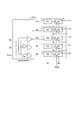
- FIG. 1 is a diagram showing a circuit block of an A / D converter according to the present embodiment.
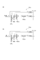
- FIG. 2 is a circuit diagram of a reference voltage generating circuit in the cyclic A / D converter shown in FIG.
- FIG. 3 is a circuit diagram of a reference voltage generation circuit in the cyclic A / D converter shown in FIG.
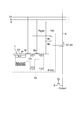
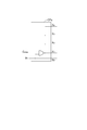
- FIG. 4 is a diagram illustrating an image sensor cell.
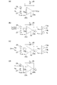
- FIG. 5 is a drawing showing the operation of integral A / D conversion in the A / D converter shown in FIG.
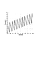
- FIG. 6 is a diagram showing input / output characteristics of the gain stage by simulation.
- FIG. 7 is a diagram showing a comparative example of the input / output characteristics of the gain stage by simulation.
- FIG. 1 is a diagram showing a circuit block of an A / D converter according to the present embodiment.
- FIG. 2 is a circuit diagram of a reference voltage generating circuit in the cyclic A / D converter shown in FIG.
- FIG. 3 is a circuit diagram
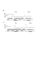
- FIG. 8 is a diagram showing processing timing in one horizontal reading period when analog CDS is performed, and a processing timing in one horizontal reading period when digital CDS is performed.
- FIG. 9 is a diagram showing an operation of cyclic A / D conversion in the A / D converter shown in FIG.
- FIG. 10 is a diagram showing an operation of integral A / D conversion in the A / D converter shown in FIG.
- FIG. 11 is a diagram showing the relationship between the input level of the analog signal VIN , which is an input signal, and the digital count value, corresponding to the simulation of FIG.
- FIG. 12 is a diagram illustrating an operation of integral A / D conversion in the A / D converter.
- FIG. 13 is a diagram showing input / output characteristics of the gain stage by simulation in the operation of the integral A / D conversion shown in FIG.
- FIG. 14 is a block diagram showing a configuration for generating a digital value from the output signal of the comparator.
- FIG. 15 is a circuit diagram of a part of the configuration shown in FIG.
- FIG. 16 is a circuit diagram of a part of the configuration shown in FIG.
- FIG. 1 is a circuit diagram of an A / D converter according to the present embodiment.
- the A / D converter 11 uses the same circuit for a first A / D conversion operation that is a so-called folding integration type A / D conversion and a second A / D conversion operation that is a cyclic A / D conversion. Implement using the configuration.
- the A / D converter 11 realizes the first and second A / D conversion operations by changing the time-series control pattern of the switches included in the A / D converter 11.
- the A / D converter 11 includes a gain stage 15, an A / D conversion circuit 17, a logic circuit 19, and a D / A conversion circuit 21.
- the A / D converter 11 includes a reference voltage generation circuit 37 and a clock generator 41.
- the gain stage 15 includes an input 15a receiving the analog signal V IN to be converted to a digital value, and an output 15b to provide a calculation value V OP.
- the gain stage 15 includes a single-ended operational amplifier circuit 23 and first to third capacitors 25, 27, and 29.
- the operational amplifier circuit 23 has a first input 23a, an output 23b, and a second input 23c.
- the phase of the signal of the output 23b is inverted from the phase of the signal applied to the first input 23a.
- the first and second inputs 23a and 23c are an inverting input terminal and a non-inverting input terminal, respectively, and the output 23b is a non-inverting output terminal.
- a second input 23c of the operational amplifier circuit 23 is connected to a reference potential line L COM, also receives a reference voltage V COM.
- the gain stage 15 includes a plurality of switches for connecting the capacitors 25, 27, and 29 and the operational amplifier circuit 23.
- the arrangement of the switches 43, 47, 49, 51, 53, and 55 shown in FIG. 1 is an example.
- the switches 43, 47, 49, 51, 53 are controlled by the clock generator 41.
- the gain stage 15 can perform the first calculation operation and the first storage operation in the first A / D conversion operation, and the second calculation operation and the second storage operation in the second A / D conversion operation.
- a second storage operation can be performed.
- the calculation value V OP is generated by the calculation amplifier circuit 23 and the first to third capacitors 25, 27, and 29.
- the first capacitor 25 is connected to the first or second reference reference voltage V RH or V RL supplied from the first output 21 a of the D / A conversion circuit 21 or the gain stage input 15 a.
- the analog signal V IN supplied from is stored.
- the second capacitor 27 stores the first or second reference reference voltages V RH and V RL supplied from the second output 21 b of the D / A conversion circuit 21.
- the third capacitor 29 is connected between the output 23b of the operational amplifier circuit 23 and the first input 23a, thereby holding the calculated value VOP .
- the first capacitor 25 is analog.
- the analog signal VIN is stored in the first capacitor 25 in the first storing operation, it is connected between the input 15a that receives the signal VIN and the first input 23a of the operational amplifier circuit 23.
- One capacitor 25 is connected between the first output 21 a of the D / A conversion circuit 21 and the first input 23 a of the operational amplifier circuit 23.
- the second capacitor 27 is connected between the second output 21 b of the D / A conversion circuit 21 and the first input 23 a of the operational amplifier circuit 23.
- the third capacitor 29 is connected between the output 23b of the operational amplifier circuit 23 and the first input 23a, so that the calculated value V OP is applied to the output 15b of the gain stage 23. Generated.
- the calculated value V OP is stored in the first and second capacitors 25 and 27.
- the calculation value V OP is generated by the calculation amplifier circuit 23 and the first to third capacitors 25, 27, and 29. That is, in the second arithmetic operation, the third capacitor 29 is connected between the output 23b of the operational amplifier circuit 23 and the first input 23a, and the first and second capacitors 25 and 27 are respectively connected to D / Connected between the first output 21 a or the second output 21 b of the A conversion circuit 21 and the first input 23 a, the calculated value V OP is generated at the output 15 b of the gain stage 15.
- the first to third capacitors 25, 27, and 29 are capacitors for storing and calculating various signal values.
- the capacitance C 2 of the third capacitor 29 is larger than the capacitances C 1a and C 1b of the first and second capacitors 25 and 27.
- the analog signal VIN input in the first A / D conversion operation that is the folding integration type A / D conversion is attenuated according to the capacitance ratio (C 1a / C 2 , C 1b / C 2 ).
- the voltage range of the analog signal VIN output in the folding integration type A / D conversion is also reduced according to the capacitance ratio of the capacitor, so that the A / D converter 11 can be configured with a single-end configuration.
- the analog signal VIN input in the folding integration type A / D conversion is attenuated by 1 ⁇ 2 and sampled and integrated.
- the voltage range of the analog signal V OP is outputted in the folding integral type A / D conversion also, since half according to the volume ratio of the capacitor, the second A / D converter is a cyclic A / D converter In operation, an input voltage suitable for a single-ended A / D converter is provided.
- the A / D conversion circuit 17 generates a digital signal D according to the conversion reference voltages V RCH and V RCL based on the signal V OP from the output 23 b of the gain stage 23.
- the A / D conversion circuit 17 can include, for example, two comparators 17a and 17b.
- the comparators 17a and 17b respectively compare the input analog signal with the respective predetermined first and second converted reference voltages V RCH and V RCL, and as shown in FIG. 1, the comparison result signals B 0 and B 1 is provided.
- the conversion reference voltages V RCH and V RCL in the A / D conversion circuit 17 are provided by the reference voltage generation circuit 37.
- the digital signal D indicates an A / D conversion value.
- the digital signal D has, for example, 2 bits (B 0 , B 1 ), and each bit (B 0 , B 1 ) can take “1” or “0”.
- the A / D conversion circuit 17 may generate the digital signal D using, for example, one comparator 17a in the first A / D conversion operation.
- the digital signal D is only 1 bit (B 1 ) and can represent a binary value.
- a signal used as a reference in the comparator 17a is a conversion reference voltage V RCH .
- the reference voltage generation circuit 37 is a circuit that generates first and second conversion reference voltages V RCH and V RCL based on the first and second reference reference voltages V RH and V RL .
- the first reference reference voltage V RH and the second reference reference voltage V RL are supplied from the reference voltage sources 33 and 35.
- FIG. 2 is an example of a circuit diagram of the reference voltage generation circuit 37.
- the reference voltage generation circuit 37 is a circuit that generates a reference voltage by dividing the first and second standard reference voltages by a ladder resistor, for example, and includes the first and second reference references.
- voltages V RC1H , V RC2H , V RC2L , and V RC1L are generated according to the resistors R 1 to R 5 having predetermined resistance values.
- the voltages V RC1H and V RC1L are supplied as the first and second conversion reference voltages V RCH and V RCL by the operation of the switch SI.
- the voltages V RC2H and V RC2L are supplied as the first and second conversion reference voltages V RCH and V RCL by the operation of the switch SA.
- the first conversion reference voltage V RCH is higher than the median value between the first reference reference voltage V RH and the second reference reference voltage value V RL and It is lower than the standard reference voltage VRH .
- the first conversion reference voltage V RCH at the first A / D conversion operation is higher than the first conversion reference voltage V RCH in the second A / D conversion operation.
- the second conversion reference voltage V RCL is lower than the median value between the first standard reference voltage V RH and the second standard reference voltage value V RL and higher than the second standard reference voltage V RL .
- the second conversion reference voltage V RCL in the first A / D conversion operation is lower than the second conversion reference voltage V RCL in the second A / D conversion operation. Since the first and second conversion reference voltages V RCH and V RCL are generated in this way, the first A / D conversion operation and the second A / D conversion operation are appropriately performed.
- V RC1H (3V RH + V RL ) / 4
- V RC1L (V RH + 3V RL ) / 4
- voltages V RC2H and V RC2L represented by the following expressions are supplied as the first and second conversion reference voltages V RCH and V RCL in the second A / D conversion operation.
- V RC2H (5V RH + 3V RL ) / 8
- V RC2L (3V RH + 5V RL ) / 8 Since the first and second conversion reference voltages V RCH and V RCL are generated in this way, the second A / D conversion operation is more appropriately performed.
- FIG. 3 shows an example of a circuit diagram of the reference voltage generation circuit 37 when the A / D conversion circuit 17 generates the digital signal D using one comparator 17a in the first A / D conversion operation. It is.
- the reference voltage generation circuit 37 in the first A / D conversion operation, the voltage V RC1H is supplied as the first conversion reference voltage V RCH by the operation of the switch SI.
- the voltages V RC2H and V RC2L are supplied as the first and second conversion reference voltages V RCH and V RCL by the operation of the switch SA.
- the first conversion reference voltage V RCH in the first A / D conversion operation is between the first standard reference voltage V RH and the second standard reference voltage value V RL. Is the median of Further, as the first and second conversion reference voltages V RCH and V RCL in the second A / D conversion operation, voltages V RC2H and V RC2L represented by the following expressions are supplied.
- V RC2H (5V RH + 3V RL ) / 8
- V RC2L (3V RH + 5V RL ) / 8
- the logic circuit 19 generates a control signal V CONT (for example, ⁇ DH , ⁇ DL , ⁇ DS ) corresponding to the digital signal D.
- V CONT for example, ⁇ DH , ⁇ DL , ⁇ DS
- D / A conversion circuit 21, first and second output 21a has 21b, at least one of the first standard reference voltage V RH and the second standard reference voltage V RL, control signal V CONT Accordingly, the gain stage 15 is provided via the first and second outputs 21a and 21b.
- the first reference voltage V RH and the second reference voltage V RL are supplied from the reference voltage sources 33 and 35.
- the D / A conversion circuit 21 provides either the first or second reference reference voltage V RH or V RL to the first output 21a and the first to the second output 21b.
- a switch circuit 31 for providing one of the second reference reference voltages V RH and V RL .
- the switch circuit 31 operates the switches 31a and 31b to supply the first and second reference reference voltages V RH and V RL to the first and second outputs 21a and 21b, respectively, and operates the switches 31a and 31c.
- the first standard reference voltage V RH the first and second output 21a by, supplied to both 21b, the switch 31b, the second standard reference voltage V RL first and by operating the 31c 2 are supplied to both outputs 21a and 21b.
- the first and second outputs 21a and 21b of the D / A conversion circuit 21 are connected to one ends 25a and 27a of the first and second capacitors 25 and 27, respectively.
- the D / A conversion circuit 21 is connected to the comparator 17a.
- the following control is performed in accordance with the control signal V CONT based on the digital signal B 1 .
- V DA1 V RH
- V DA2 V RL
- FIG. 4 is a diagram illustrating pixels of the image sensor.
- the image sensor device includes a cell array including an array of image sensor cells 2a, and a converter array connected to the cell array and including a plurality of A / D converters 11. Each of the A / D converters 11 is connected to the image sensor cell 2a via the column line 8 of the cell array.
- the image sensor cell 2a has, for example, a CMOS image sensor cell structure.
- the photodiode DF receives light L for one pixel related to the image.
- the gate of the selection transistor M S is connected to the row select line S extending in the row direction.
- the gate of the reset transistor M R is connected to the reset line R.
- the gate of the transfer transistor M T is connected to the transfer selection line extending in the row direction.
- One end of the photodiode DF is connected to the floating diffusion layer FD via the transfer transistor M T.
- Floating diffusion layer FD is connected to a reset potential line Reset via the reset transistor M R, is connected to the gate of the transistor M A.
- One current terminal (for example, drain) of the transistor M A is connected to the column line 8 via the selection transistor M S.
- Transistor M A is provided in the column line through the selection transistor M S a potential corresponding to the charge amount of the floating diffusion layer FD.
- the image sensor cell 2a having this structure can generate a first signal indicating a reset level and a second signal indicating a signal level superimposed on the reset level. That is, the image sensor cell 2a, first, providing a reset control signal R to the reset transistor M R, resets the floating diffusion layer FD. Through the amplification transistor M A, read out the reset level. Then, a charge transfer control signal TX is supplied to the transfer transistor M T, is transferred from the photodiode DF photoinduced signal charges to the floating diffusion layer. Thereafter, through the transistor M A, reading the signal level. Thus, the pixel 2a can generate the first signal S1 indicating the reset level and the second signal S2 indicating the signal level superimposed on the reset level.
- the A / D converter 11 performs a first storing operation as a first initial storing step.
- the analog signal VIN received via the input 15a of the gain stage 15 is stored in the first capacitor 25, and the output 23b of the gain stage 15 and the first input 23a are connected.
- the second capacitor 27 stores the second reference voltage VRL supplied from the second output 21b, and the third capacitor 29 includes the output 23b of the operational amplifier circuit 23 and the first input 23a. Connected between.
- the first calculation operation is performed by connecting the first capacitor 25 between the first output 21a and the first input 23a.
- the second capacitor 27 is connected between the second output 21b and the first input 23a, and the third capacitor 29 is connected between the output 23b of the operational amplifier circuit 23 and the first input 23a.
- the calculated value V OP is generated at the output 15 b of the gain stage 15.
- a reference reference voltage V RH or a second reference reference voltage V RL is provided.
- V OP V COM
- the output V OP at this time is as follows.
- the A / D converter 11 performs the first storing operation shown in FIG. 5D as the first storing step.
- the first storage step while retaining the operation value V OP to the capacitance C 2 by connecting the third capacitor 29 between the output 23b and the first input 23a of the operational amplifier circuit 23, the gain stage The analog signal VIN from the 15 inputs 15 a is stored in the first capacitor 25, and the second reference voltage V RL supplied from the second output 21 b is stored in the second capacitor 27.
- the A / D converter 11 performs the first calculation operation as the first calculation step shown in FIG. 5B or 5C. That is, the A / D converter 11 selects the first calculation step while selecting one of the first calculation operations shown in FIGS. 5B and 5C according to the value of the output value D. And an integration type A / D conversion step in which the first storing step is repeated a predetermined number of times.
- the integration type A / D conversion step the calculation value VOP when the first calculation step and the first storage step are repeated M times to perform sampling and integration is expressed by the following equation (7).
- the analog signal VIN that is the input signal is multiplied by a half gain, sampling is performed M times, and folding integration type A / D conversion is performed. And the amplitude range of the output (calculated value V OP ) is the same as the input signal.
- FIG. 6 is a diagram showing input / output characteristics at the time of an operation (folding integration type A / D conversion) of the gain stage 15 obtained by simulation as an integration type A / D converter.
- FIG. 6 (a) the output is 1 to 2V with respect to the input of 1.5V to 2.5V and the amplitude is 1V, and the amplitude is within the range of 1V.
- the second reference voltage VRL is adopted as the reference voltage VRI in the arithmetic operation. That is, in FIGS. 5A and 5D, the second reference reference voltage VRL is supplied to the second capacitor 27.
- the first reference voltage VRH may be adopted as the reference voltage VRI in the calculation operation.
- the absolute value of the output is different from that when the second standard reference voltage V RL is employed. In this case, the equation (7) is transformed into the following equation (8).
- the first and second conversion reference voltages V RCH and V RCL supplied to the comparators 17a and 17b are changed as compared with the input / output characteristics shown in FIG. Shown in In the example of the input / output characteristics shown in FIG. 6A , the first and second conversion reference voltages V RCH and V RCL have the values shown below.
- the first and second conversion reference voltages V RCH and V RCL are values shown below.
- the first and second conversion reference voltages V RCH and V RCL are preferably set to values as when the input / output characteristics of FIG. 6A are obtained.
- FIG. 8A is a diagram illustrating processing timing in one horizontal readout period when analog CDS is performed.
- FIG. 8B is a diagram showing processing timing in one horizontal readout period when digital CDS is performed.
- an analog signal V IN that is input to the gain stage 15 is a first signal that is output from the image sensor cell and indicates a reset level in the period S fr1 .
- Integral A / D conversion is performed (first reset level integral A / D conversion step).
- the integration type A / D conversion is performed by using the second signal indicating the signal level superimposed on the reset level as the analog signal VIN input to the gain stage 15 (first signal).
- Level integration type A / D conversion step In the first signal level integration type A / D conversion step, as described later with reference to FIG. 9, the polarity of the charge transferred to the third capacitor 29 serving as an integrator is changed to the first reset level.
- the calculation is performed so as to be opposite to the level integration type A / D conversion step. Thereby, the value of the upper bit in the digital value obtained by A / D converting the signal level is obtained. In the digital value obtained here, noise is canceled. Then, in the period Scs1 , cyclic A / D conversion is performed using a residual analog signal obtained as a result of the first signal level integration A / D conversion step as an input signal. Thereby, the value of the lower bit in the digital value obtained by A / D converting the signal level is obtained.
- Integral A / D conversion is performed as VIN (integral A / D conversion step for the first signal). Thereby, the value of the upper bit in the digital value obtained by A / D converting the reset level is obtained.
- cyclic A / D conversion is performed using the residual analog signal obtained as a result of the integral A / D conversion step for the first signal as an input signal (cyclic for the first signal).
- Type A / D conversion step Thereby, the value of the lower bit in the digital value obtained by A / D converting the reset level is obtained. Accordingly, a digital value obtained by A / D-converting the reset level is obtained in the period S fr2 and the period S cr2 .
- integral A / D conversion is performed using the second signal indicating the signal level superimposed on the reset level as the analog signal VIN input to the gain stage 15 (second signal). Integration type A / D conversion step). Thereby, the value of the upper bit in the digital value obtained by A / D converting the second signal is obtained. Then, in the period Scs2 , cyclic A / D conversion is performed using a residual analog signal obtained as a result of the integral A / D conversion step for the second signal as an input signal. Thereby, the value of the lower bit in the digital value obtained by A / D converting the second signal is obtained.
- a digital value obtained by A / D converting the reset signal is obtained in the period Sfs2 and the period Scs2 . Accordingly, a digital value obtained by A / D converting the second signal is obtained in the period Sfs2 and the period Scs2 . Then, by subtracting the digital value obtained in the period S fr2 and the period S cr2 from the digital value obtained in the period S fs2 and the period S cs2 , the signal level in which the output variation and noise between cells are canceled. Can be obtained.
- This cyclic A / D conversion is performed, for example, in the periods S cs1 , S cr2 , S cs2 in FIG.
- the gain stage 15 performs a second storing operation as a second initial storing step as shown in FIG.
- the residual analog that is the calculation value V OP in the first signal level integration type A / D conversion step (period S fs1 ) or the integration type A / D conversion step (period S fr2 or period S fs2 ).
- the signal is stored in the first, second and third capacitors 25, 27 and 29.
- the switches 31c, 47, 51 are turned on, and the switches 31a, 31b, 43, 49, 53 are turned off.
- the operation value V OP in the first signal level integration type A / D conversion step or the integration type A / D conversion step is provided to the comparators 17a and 17b.
- the comparators 17a and 17b generate digital signals B 1 and B 0 based on the provided operation value V OP .
- the second calculation operation is performed.
- the gain stage 15 generates a calculation value V OP by the calculation amplifier circuit 23 and the capacitors 25, 27, and 29.
- the third capacitor 29 is connected between the output 15b of the operational amplifier circuit 15 and the input 15a, and the first capacitor 25 is connected to the first output 21a and the first input 23a.
- the second capacitor 27 is connected between the second output 21b and the first input 23a.
- D the output value
- a voltage V RH or a second reference voltage V RL is provided.
- the comparators 17a and 17b operate as follows.
- the gain stage 15 performs the second storage operation as the second storage step shown in FIG. 9A following the second calculation step.
- the second storage step is different from the second initial storage step in that the calculation value V OP in the second calculation step is stored in the first, second, and third capacitors 25, 27, and 29.
- the gain stage 15 repeats the second calculation step and the second storage step a predetermined number of times as a cyclic A / D conversion step.
- FIG. 10 shows an example of the integral type A / D conversion operation for the second signal indicating the signal level superimposed on the reset level when the analog CDS is performed as described above.
- the polarity of the charge transferred to the capacitor constituting the integrator is opposite to the integral A / D conversion (see FIG. 5) performed on the first signal indicating the reset level.
- An A / D conversion operation is performed.
- the gain stage 15 stores the first signal level storage shown in FIG. 10 (a) or FIG. 10 (b) according to the value of the output value D in the calculation operation one step before.
- a first storing operation as a step is performed.
- the gain stage 15 connects the third capacitor 29 between the output 23b of the operational amplifier circuit 23 and the first input 23a, so that in the first reset level integral A / D conversion step.
- the first reference reference voltage V RH or the second reference reference voltage V RL supplied from the first output 21 a is stored in the first capacitor 25 while the calculated value V OP is held in the capacitor C 2 .
- the first reference reference voltage V RH or the second reference reference voltage V RL supplied from the second output 21 b is stored in the second capacitor 27.
- the gain stage 15 performs a first calculation operation as a first signal level calculation step shown in FIG.
- the gain stage 15 connects the first capacitor 25 between the input VIN of the gain stage 15 to which the second signal is supplied and the first input 23a, and the second output 21b and the second output 21b.
- a second capacitor 27 is connected between the first input 23a.
- the analog signal VIN and the reference voltage V RI in the operational amplifier circuit 23 are changed to the first and second capacitors 25 and 27.
- the charge related to the analog signal VIN is transferred to the integrator with the opposite polarity to the integral type A / D conversion shown in FIG.
- the analog signal VIN provided to the input 15a of the gain stage 15 is a reset level signal VRES .
- the analog signal VIN provided to the input 15a of the gain stage 15 is a signal level signal V SIG . Therefore, the expression (10) is expressed as the expression (12).
- Formula (12) is represented as the following Formula (13).
- Expression (13) is expressed as Expression (14) below using Expression (6).
- the digital value for M (V RES ⁇ V SIG ) to be obtained is expressed by the result of the cyclic A / D conversion and the result of the folding integration A / D conversion (digital count value). Means that. If the result of the folding integration type A / D conversion is n bits, the A / D converter 11 of the present embodiment can perform A / D conversion to obtain a digital value of (n + m ⁇ 1) bits.
- the digital count value which is the result of the folding integration type A / D conversion, appears as 1 in the output value D (B 1 + B 0 or B 1 ) by the counter circuit provided at the subsequent stage of the A / D conversion circuit 17. It is obtained by acquiring the number of times. The acquisition of the count value will be described later.
- FIG. 11 is a diagram showing the relationship between the input level of the analog signal VIN , which is an input signal corresponding to the simulation of FIG. 6, and the digital count value.
- the digital count value takes a value of 15 gradations for 16 samplings and integrations in the integral type A / D conversion and an input range of 1.0V. obtain. Therefore, the range of this digital count value is represented by about 4 bits.
- This term can be a value in the range of 0 to 14 when the input level range is 1.0 V, and is represented by 4 bits. Therefore, for example, when the cyclic A / D conversion is performed so that a 12-bit output result is obtained, the higher order bits of the counter value are shifted by 1 bit to generate a linear signal.
- the gain stage 15 performs a first storing operation as a first initial storing step.
- the analog signal VIN received via the input 15a of the gain stage 15 is stored in the first capacitor 25, and the output 23b of the gain stage 15 and the first input 23a are connected.
- the second capacitor 27 stores the second reference voltage VRL supplied from the second output 21b, and the third capacitor 29 includes the output 23b of the operational amplifier circuit 23 and the first input 23a. Connected between.
- the first calculation operation is performed by connecting the first capacitor 25 between the first output 21a and the first input 23a.
- the second capacitor 27 is connected between the second output 21b and the first input 23a, and the third capacitor 29 is connected between the output 23b of the operational amplifier circuit 23 and the first input 23a.
- the calculated value V OP is generated at the output 15 b of the gain stage 15.
- RH or a second reference voltage VRL is provided.
- the first reference reference voltage V RH and the second reference reference voltage V RL are respectively obtained from the first output 21a and the second output 21b of the D / A conversion circuit 21.
- the operation shown in FIG. 12B is performed while being controlled to be provided.
- the second reference reference voltage VRL is controlled so as to be provided from the first output 21a and the second output 21b of the D / A conversion circuit 21 as shown in FIG. Operation is performed.
- the gain stage 15 performs the first storing operation shown in FIG. 12D as a first storing step.
- the first storage step while retaining the operation value V OP to the capacitance C 2 by connecting the third capacitor 29 between the output 23b and the first input 23a of the operational amplifier circuit 23, the gain stage The analog signal VIN from the 15 inputs 15 a is stored in the first capacitor 25, and the second reference voltage V RL supplied from the second output 21 b is stored in the second capacitor 27.
- the gain stage 15 selects the first calculation step and the first calculation while selecting one of the first calculation operations shown in FIGS. 12B and 12C according to the value of the output value D.
- the integration type A / D conversion step is performed by repeating the storing step a predetermined number of times.
- FIG. 13 shows an operation of the gain stage 15 as an integration type A / D converter (folding integration type A / D conversion) when the A / D conversion circuit 17 generates the digital signal D using one comparator 17a.
- the output is 1.5 to 2.5 V with respect to the input of 1.5 to 2.5 V and the amplitude is 1 V, and the amplitude is within the range of 1 V. .
- FIG. 14A is a diagram showing the digital unit DC A when the A / D conversion circuit 17 generates the digital signal D using the two comparators 17a and 17b and the two conversion reference voltages V RCH and V RCL . is there.
- the digital part DC A includes a complement part CP A , an adder AD A , a register RG 1A, and a register RG 2A .
- FIG. 15 is a diagram showing a detailed configuration of the complement unit CP A , the adder AD A , and the register RG 1A shown in FIG. In the example shown in FIG. 15, a 5-bit digital value is obtained. The operation of these configurations will be described below with reference to FIGS. 14 (a) and 15.
- a reset signal reset is given to a 5-bit register RG 1A (consisting of five flip-flops FF), and their outputs are set to zero.
- the output of the register RG 1A and the 2-bit outputs (B1, B0) from the two comparators 17a and 17b of the integration type A / D conversion are added to the adder AD.
- A is added by A (consisting of five full adders FA), a clock is further added, and the output result is stored in the register RG 1A .
- a signal Comp provided to complement portion CP A is set to 0.
- the value is incremented by -1.
- the value is added by -2.
- Register RG 2A stores a digital value obtained as a result of cyclic A / D conversion.
- FIG. 14 (b) is a diagram illustrating a digital section DC B in the A / D conversion circuit 17 generates a digital signal D by using one comparator 17a and one conversion reference voltage V RCH.
- the digital part DC B includes a complement part CP B , an adder AD B , a register RG 1B, and a register RG 2B .
- FIG. 16 is a diagram showing a detailed configuration of the complement unit CP B shown in FIG.
- the configurations of the adder AD B and the register RG 1B are the same as those shown in FIG. In the example shown in FIG. 16, a 5-bit digital value is obtained.
- FIGS the operation of these configurations will be described with reference to FIGS.
- a reset signal reset is given to a 5-bit register RG 1B (consisting of five flip-flops FF), and their outputs are set to zero.
- the output of the register RG 1B and the 1-bit output (B1) from one comparator 17a of the integration type A / D conversion are added to the adder AD B (5 And the output result is stored in the register RG 1B .
- the 1-bit output is digitally integrated.
- Register RG 2B stores a digital value obtained as a result of cyclic A / D conversion.
- the first A / D conversion for performing the folding integration type A / D conversion is performed by controlling the operation procedure in the same circuit configuration.
- the operation and the second A / D conversion operation for performing the cyclic A / D conversion are realized.
- the capacitance of the third capacitor 29 used for integration of the output signal is the first and second used for storing the analog signal to be A / D converted and the reference reference voltage. Therefore, the analog signal VIN input in the folding integration type A / D conversion is attenuated according to the capacitance ratio and sampled and integrated. Therefore, the voltage range of the analog signal output in the folding integration type A / D conversion is also reduced in accordance with the capacitance ratio of the capacitor, so that the A / D converter can be configured with a single end configuration.
- an A / D converter that performs A / D conversion by folding integration and cyclic A / D conversion on the residual analog signal can be realized by a single-ended configuration. It becomes possible.
Landscapes
- Engineering & Computer Science (AREA)
- Theoretical Computer Science (AREA)
- Multimedia (AREA)
- Signal Processing (AREA)
- Analogue/Digital Conversion (AREA)
Abstract
Description
VRC2H=(5VRH+3VRL)/8
VRC2L=(3VRH+5VRL)/8
このA/D変換器によれば、適切に第2のA/D変換動作が実施される。
VRC1H=(3VRH+VRL)/4
VRC1L=(VRH+3VRL)/4
第2のA/D変換動作における第1の変換参照電圧VRC2Hは及び第2の変換参照電圧VRC2Lはそれぞれ下記式により表される。
VRC2H=(5VRH+3VRL)/8
VRC2L=(3VRH+5VRL)/8
このA/D変換器によれば、適切に第2のA/D変換動作が実施される。
VOP>VRCHのとき B1=1,B0=1
VRCL<VOP≦VRCHのとき B1=0,B0=1
VOP≦VRCLのとき B1=0,B0=0
VOP>VRCHのとき B1=1
VOP≦VRCHのとき B1=0
VRC1H=(3VRH+VRL)/4
VRC1L=(VRH+3VRL)/4
また、第2のA/D変換動作における第1及び第2の変換参照電圧VRCH、VRCLとして、以下の式により表される電圧VRC2H,VRC2Lが供給されることが好ましい。
VRC2H=(5VRH+3VRL)/8
VRC2L=(3VRH+5VRL)/8
このように第1及び第2の変換参照電圧VRCH、VRCLが生成されるので、より適切に第2のA/D変換動作が実施される。
VRC2H=(5VRH+3VRL)/8
VRC2L=(3VRH+5VRL)/8
条件D=2が満たされるとき:VDA1=VDA2=VRH
条件D=1が満たされるとき:VDA1=VRH、VDA2=VRL
条件D=0が満たされるとき:VDA1=VDA2=VRL
といった制御を行う。
条件B1=1が満たされるとき:VDA1=VRH、VDA2=VRL
条件B1=0が満たされるとき:VDA1=VDA2=VRL
Q1a=C1a(VIN-VCOM) …(1)
Q1b=C1b(VRL-VCOM) …(2)
となる。
VOP>VRCHのとき B1=1,B0=1
VRCL<VOP≦VRCHのとき B1=0,B0=1
VOP≦VRCLのとき B1=0,B0=0 …(3)


ここで、式(5)におけるΔVRは以下の式(6)により表される。



VRCH=(3VRH+VRL)/4=1.75V
VRCL=(VRH+3VRL)/4=1.25V
これに対して、図7に示す入出力特性の例では、第1及び第2の変換参照電圧VRCH、VRCLは、以下に示す値である。
VRCH=(5VRH+3VRL)/8=1.625V
VRCL=(3VRH+5VRL)/8=1.375V
図7に示されるように、第1及び第2の変換参照電圧VRCH、VRCLが変更されると、ゲインステージ15における積分型A/D変換が好適に実施されない。従って、第1及び第2の変換参照電圧VRCH、VRCLは、図6(a)の入出力特性が得られたときのような値に設定されることが好ましい。
VOP>VRCHのとき D=2(B1=1,B0=1)
VRCL<VOP≦VRCHのとき D=1(B1=0,B0=1)
VOP≦VRCLのとき D=0(B1=0,B0=0)

さらに、第1の信号レベル用演算ステップ及び第1の信号レベル用格納ステップをM回繰り返したときの演算値VOP(2M)は、以下の式(10)により表される。

また、VRI=VRHである場合には、式(10)は、以下の式(11)のように変形される。


さらに、式(12)は、以下の式(13)のように表される。

さらに、式(13)は、式(6)を用いて、以下の式(14)のように表される。


ここで、かっこ[]は、かっこ内の値のディジタル値を意味する。
さらに、値Yを式(16)のように表す。

式(14)は、値X,Yを用いて、以下の式(17)のように表される。


の項は、入力レベルの範囲が1.0Vである場合に、0~14の範囲の値を取りうるので、4ビットで表される。従って、例えば、巡回型A/D変換を12ビットの出力結果が得られるように実施した場合には、カウンタ値の上位ビットを1ビットシフトして線形の信号を生成することから、本実施形態のA/D変換器11は、15ビット(=(12+4-1)ビット)にほぼ相当するダイナミックレンジを有することができる。以上説明したように、本実施形態のA/D変換器11は、フォールディング積分型のA/D変換である積分型A/D変換によるノイズ低減の効果を十分に得ながら、広いダイナミックレンジを有するディジタル信号の出力をすることができる。
VOP>VRCHのとき B1=1
VOP≦VRCHのとき B1=0
Claims (11)
- シングルエンド構成のA/D変換器であって、
ディジタル値に変換されるアナログ信号を受ける入力、出力、並びに第1の入力、第2の入力及び出力を有する演算増幅回路を含むゲインステージと、
前記ゲインステージの前記出力からの信号に基づき、変換参照電圧を参照して、1又は複数のビットを含むディジタル信号を生成するA/D変換回路と、
前記ディジタル信号に応じて、制御信号を生成する論理回路と、
第1及び第2の出力を有し、第1の基準参照電圧及び第2の基準参照電圧の少なくともいずれか一方を、前記制御信号に応じて前記第1及び第2の出力を介して前記ゲインステージに提供するD/A変換回路とを備え、
前記ゲインステージは、第1~第3のキャパシタを含み、
前記第3のキャパシタの容量は、前記第1及び第2のキャパシタの容量より大きく、
前記演算増幅回路の前記第2の入力は、基準電位を受け、
前記第1の基準参照電圧は、前記第2の基準参照電圧値より高く、
前記D/A変換回路は、前記制御信号に応答して、前記第1の出力に前記第1及び第2の基準参照電圧のいずれかを提供すると共に前記第2の出力に前記第1及び第2の基準参照電圧のいずれかを提供するためのスイッチ回路を含み、
当該A/D変換器は、第1のA/D変換動作と、第2のA/D変換動作を行い、
前記第1のA/D変換動作では、前記ゲインステージは、前記演算増幅回路及び前記第1~第3のキャパシタにより演算値を生成する第1の演算動作と、第1の格納動作と、を行い、
前記第1の格納動作では、
前記第1のキャパシタは、前記第1の出力から供給される第1若しくは第2の基準参照電圧又は前記アナログ信号を格納し、
前記第2のキャパシタは、前記第2の出力から供給される第1又は第2の基準参照電圧を格納し、
前記第3のキャパシタは、前記演算増幅回路の前記出力と前記第1の入力との間に接続され、
前記第1の演算動作では、
前記第1の格納動作において第1又は第2の基準参照電圧が前記第1のキャパシタに格納された場合には、前記第1のキャパシタが前記アナログ信号を受ける入力と前記第1の入力との間に接続され、前記第1の格納動作において前記アナログ信号が前記第1のキャパシタに格納された場合には、前記第1のキャパシタが前記第1の出力と前記第1の入力との間に接続され、
前記第2のキャパシタが前記第2の出力と前記第1の入力との間に接続され、
前記第3のキャパシタが前記演算増幅回路の前記出力と前記第1の入力との間に接続されることにより、前記演算値が前記ゲインステージの前記出力に生成され、
前記第2のA/D変換動作では、
前記ゲインステージは、前記演算増幅回路及び前記第1~第3のキャパシタにより演算値を生成する第2の演算動作と、前記演算値を前記第1及び第2のキャパシタに格納する第2の格納動作を行い、
前記第2の演算動作では、前記第3のキャパシタが前記演算増幅回路の前記出力と前記第1の入力との間に接続されると共に前記第1及び第2のキャパシタがそれぞれ前記D/A変換回路の前記第1又は第2の出力と前記第1の入力との間に接続されて、前記演算値が当該ゲインステージの前記出力に生成される、
A/D変換器。 - 前記第3のキャパシタは、前記第1又は第2のキャパシタの容量の2倍の容量を有する、
請求項1に記載のA/D変換器。 - 前記第1のA/D変換動作における前記変換参照電圧は、前記第1の基準参照電圧と前記第2の基準参照電圧値との間の中央値であり、
前記A/D変換回路は、1ビットのディジタル信号を生成し、
前記論理回路は、第1及び第2の値を有する制御信号を生成する、
請求項1又は2に記載のA/D変換器。 - 前記第2のA/D変換動作において参照される第1の変換参照電圧VRC2Hは及び第2の変換参照電圧VRC2Lはそれぞれ下記式により表される、
VRC2H=(5VRH+3VRL)/8
VRC2L=(3VRH+5VRL)/8
請求項3に記載のA/D変換器。 - 前記A/D変換回路は、第1及び第2の変換参照電圧を有し、
前記第1の変換参照電圧は、前記第1の基準参照電圧と前記第2の基準参照電圧値との間の中央値より高く且つ前記第1の基準参照電圧より低く、
前記第1のA/D変換動作における前記第1の変換参照電圧は、前記第2のA/D変換動作における前記第1の変換参照電圧より高く、
前記第2の変換参照電圧は、前記中央値より低く且つ前記第2の基準参照電圧より高く、
前記第1のA/D変換動作における前記第2の変換参照電圧は、前記第2のA/D変換動作における前記第2の変換参照電圧より低く、
前記A/D変換回路は、3値のディジタル信号を生成し、
前記論理回路は、第1~第3の値を有する制御信号を生成する、
請求項1又は2に記載のA/D変換器。 - 前記第1の基準参照電圧をVRH、前記第2の基準参照電圧をVRL、としたときに、
前記第1のA/D変換動作における前記第1の変換参照電圧VRC1H及び前記第2の変換参照電圧VRC1Lはそれぞれ下記式により表され、
VRC1H=(3VRH+VRL)/4
VRC1L=(VRH+3VRL)/4
前記第2のA/D変換動作における前記第1の変換参照電圧VRC2Hは及び前記第2の変換参照電圧VRC2Lはそれぞれ下記式により表される、
VRC2H=(5VRH+3VRL)/8
VRC2L=(3VRH+5VRL)/8
請求項5に記載のA/D変換器。 - 前記第1の格納動作では、前記第1のキャパシタは、前記第1の出力又は前記ゲインステージの入力と前記基準電位との間に接続され、前記第2のキャパシタは、前記第2の出力又は前記ゲインステージの入力と前記基準電位との間に接続される、
請求項1~6のいずれか1項に記載のA/D変換器。 - シングルエンド構成のA/D変換器であって、
ディジタル値に変換されるアナログ信号を受ける入力、出力、並びに第1の入力、第2の入力及び出力を有する演算増幅回路を含むゲインステージと、
前記ゲインステージの前記出力からの信号に基づき、変換参照電圧を参照して、1又は複数のビットを含むディジタル信号を生成するA/D変換回路と、
前記ディジタル信号に応じて、制御信号を生成する論理回路と、
第1及び第2の出力を有し、第1の基準参照電圧及び第2の基準参照電圧の少なくともいずれか一方を、前記制御信号に応じて前記第1及び第2の出力を介して前記ゲインステージに提供するD/A変換回路と、
前記第1及び第2の基準参照電圧を分圧して前記変換参照電圧を生成する参照電圧発生回路と、を備え、
前記ゲインステージは、第1~第3のキャパシタを含み、
前記第3のキャパシタの容量は、前記第1及び第2のキャパシタの容量より大きく、
前記演算増幅回路の前記第2の入力は、基準電位を受け、
前記第1の基準参照電圧は、前記第2の基準参照電圧値より高く、
前記D/A変換回路は、前記制御信号に応答して、前記第1の出力に前記第1及び第2の基準参照電圧のいずれかを提供すると共に前記第2の出力に前記第1及び第2の基準参照電圧のいずれかを提供するためのスイッチ回路を含み、
当該A/D変換器は、一の変換参照電圧、又は第1及び第2の変換参照電圧を参照して1ビットまたは3値のディジタル信号を前記A/D変換回路に生成させる第1のA/D変換動作と、第1及び第2の変換参照電圧を参照して3値のディジタル信号を前記A/D変換回路に生成させる第2のA/D変換動作とを行い、
前記参照電圧発生回路は、
前記第1の基準参照電圧と前記第2の基準参照電圧値との間の中央値より高く且つ前記第1の基準参照電圧より低い電圧を前記第2のA/D変換動作のための前記第1の変換参照電圧として生成すると共に、前記中央値より低く且つ前記第2の基準参照電圧より高い電圧を前記第2のA/D変換動作のための前記第2の変換参照電圧として生成し、
前記中央値を前記第1のA/D変換のための前記一の変換参照電圧として生成、又は前記第2のA/D変換動作のための前記第1の変換参照電圧より高く且つ前記第1の基準参照電圧より低い電圧を、前記第1の変換動作のための前記第1の変換参照電圧として生成すると共に前記第2のA/D変換動作のための前記第2の変換参照電圧より低く且つ前記第2の基準参照電圧より高い電圧を、前記第1の変換動作のための前記第2の変換参照電圧として生成する、
A/D変換器。 - イメージセンサデバイスであって、
イメージセンサセルのアレイを含むセルアレイと、
前記セルアレイに接続されており複数のA/D変換器を含む変換器アレイとを備え、
前記A/D変換器の各々は、前記セルアレイのカラム線を介して前記イメージセンサセルに接続されており、
前記A/D変換器の各々は、請求項1~8のいずれか1項に記載されたものである、
イメージセンサデバイス。 - 請求項1~8のいずれか1項に記載のA/D変換器を用いてアナログ信号からディジタル信号を生成する方法であって、
前記ゲインステージの入力からの前記アナログ信号を前記第1のキャパシタに格納し、前記演算増幅回路の出力と前記第1の入力とを接続して前記第1の格納動作を行う第1の初期格納ステップと、
前記第1のキャパシタを前記第1の出力と前記第1の入力との間に接続して前記第1の演算動作を行う第1の演算ステップと、
前記ゲインステージの入力からの前記アナログ信号を前記第1のキャパシタに格納して前記第1の格納動作を行う第1の格納ステップと、
前記第1の演算ステップ及び第1の格納ステップを所定回数繰り返して行う積分型A/D変換ステップと、
前記積分型A/D変換ステップにおける演算値である残差アナログ信号を前記第1及び第2のキャパシタに格納して前記第2の格納動作を行う第2の初期格納ステップと、
前記第2の演算動作を行う第2の演算ステップと、
前記第2の演算ステップにおいて前記ゲインステージの出力に生成された前記演算値を前記第1及び第2のキャパシタに格納して前記第2の格納動作を行う第2の格納ステップと、
前記第2の演算ステップ及び第2の格納ステップを所定回数繰り返して行う巡回型A/D変換ステップと、
を有する方法。 - 請求項1~8のいずれか1項に記載のA/D変換器を用いて、イメージセンサセルのアレイを含むイメージセンサデバイスからのアナログ信号からデジタル信号を生成する方法であって、
前記イメージセンサセルは、リセットレベルを示す第1の信号と該リセットレベルに重畳された信号レベルを示す第2の信号とを生成可能であり、
前記ゲインステージの入力を介して受けた前記第1の信号を前記第1のキャパシタに格納し、前記演算増幅回路の出力と前記第1の入力とを接続して前記第1の格納動作を行う第1の初期格納ステップと、
前記第1のキャパシタを前記第1の出力と前記第1の入力との間に接続して前記第1の演算動作を行う第1のリセットレベル用演算ステップと、
前記ゲインステージの入力からの前記アナログ信号を前記第1のキャパシタに格納して前記第1の格納動作を行う第1のリセットレベル用格納ステップと、
前記第1のリセットレベル用演算ステップ及び第1のリセットレベル用格納ステップを所定回数繰り返して行う第1のリセットレベル用積分型A/D変換ステップと、
前記第1の出力から供給される第1若しくは第2の基準参照電圧を前記第1のキャパシタに格納して前記第1の格納動作を行う第1の信号レベル用格納ステップと、
前記第2の信号が供給された前記ゲインステージの入力と前記第1の入力との間に前記第1のキャパシタを接続して前記第1の演算動作を行う第1の信号レベル用演算ステップと、
前記第1の信号レベル用演算ステップ及び第1の信号レベル用格納ステップを所定回数繰り返して行う第1の信号レベル用積分型A/D変換ステップと、
前記第1の信号レベル用積分型A/D変換ステップにおける演算値である残差アナログ信号を前記第1及び第2のキャパシタに格納して前記第2の格納動作を行う第2の初期格納ステップと、
前記第2の演算動作を行う第2の演算ステップと、
前記第2の演算ステップにおいて前記ゲインステージの出力に生成された前記演算値を前記第1及び第2のキャパシタに格納して前記第2の格納動作を行う第2の格納ステップと、
前記第2の演算ステップ及び第2の格納ステップを所定回数繰り返して行う巡回型A/D変換ステップと、
を有する方法。
Priority Applications (4)
| Application Number | Priority Date | Filing Date | Title |
|---|---|---|---|
| EP12747652.1A EP2677661A4 (en) | 2011-02-18 | 2012-02-17 | A/d converter, image sensor device, and method of generating digital signal from analog signal |
| KR1020137021590A KR101743800B1 (ko) | 2011-02-18 | 2012-02-17 | A/d 변환기, 이미지 센서 디바이스 및 아날로그 신호로부터 디지털 신호를 생성하는 방법 |
| JP2012558044A JP5818170B2 (ja) | 2011-02-18 | 2012-02-17 | A/d変換器、イメージセンサデバイス及びアナログ信号からディジタル信号を生成する方法 |
| US13/985,723 US9236879B2 (en) | 2011-02-18 | 2012-02-17 | A/D converter, image sensor device, and method of generating digital signal from analog signal |
Applications Claiming Priority (2)
| Application Number | Priority Date | Filing Date | Title |
|---|---|---|---|
| JP2011033718 | 2011-02-18 | ||
| JP2011-033718 | 2011-02-18 |
Publications (1)
| Publication Number | Publication Date |
|---|---|
| WO2012111821A1 true WO2012111821A1 (ja) | 2012-08-23 |
Family
ID=46672731
Family Applications (1)
| Application Number | Title | Priority Date | Filing Date |
|---|---|---|---|
| PCT/JP2012/053868 Ceased WO2012111821A1 (ja) | 2011-02-18 | 2012-02-17 | A/d変換器、イメージセンサデバイス及びアナログ信号からディジタル信号を生成する方法 |
Country Status (5)
| Country | Link |
|---|---|
| US (1) | US9236879B2 (ja) |
| EP (1) | EP2677661A4 (ja) |
| JP (1) | JP5818170B2 (ja) |
| KR (1) | KR101743800B1 (ja) |
| WO (1) | WO2012111821A1 (ja) |
Cited By (3)
| Publication number | Priority date | Publication date | Assignee | Title |
|---|---|---|---|---|
| JP2014239426A (ja) * | 2013-05-09 | 2014-12-18 | 株式会社ブルックマンテクノロジ | A/d変換回路用ディジタル補正回路、a/d変換回路及びイメージセンサデバイス |
| JP2015053648A (ja) * | 2013-09-09 | 2015-03-19 | オリンパス株式会社 | 撮像装置 |
| JP2017139583A (ja) * | 2016-02-02 | 2017-08-10 | 国立大学法人静岡大学 | A/d変換器、イメージセンサデバイス及びアナログ信号からディジタル信号を生成する方法 |
Families Citing this family (7)
| Publication number | Priority date | Publication date | Assignee | Title |
|---|---|---|---|---|
| US9560523B2 (en) * | 2013-08-23 | 2017-01-31 | General Electric Company | Mobile device authentication |
| US9148481B1 (en) | 2014-09-04 | 2015-09-29 | Sandia Corporation | Embedded instrumentation architecture |
| KR101723624B1 (ko) | 2015-10-08 | 2017-04-06 | 동국대학교 산학협력단 | 싸이클릭 디지털-아날로그 변환기의 코어 회로 및 이를 포함하는 디지털-아날로그 변환기 |
| US10715757B2 (en) * | 2016-11-11 | 2020-07-14 | National University Corporation Shizuoka University | A/D converter |
| TWI638529B (zh) * | 2017-10-25 | 2018-10-11 | 瑞昱半導體股份有限公司 | 可彈性切換候選電容的運算放大器 |
| TWI645681B (zh) * | 2017-10-25 | 2018-12-21 | 瑞昱半導體股份有限公司 | 運算放大器可供不同電路級共用的管線式類比數位轉換器 |
| EP3557767B1 (en) * | 2018-04-19 | 2023-01-11 | ams AG | Light-to-digital converter arrangement and method for light-to-digital conversion |
Citations (2)
| Publication number | Priority date | Publication date | Assignee | Title |
|---|---|---|---|---|
| JP2004096636A (ja) * | 2002-09-03 | 2004-03-25 | Sanyo Electric Co Ltd | アナログ−デジタル変換回路 |
| WO2008016049A1 (fr) | 2006-07-31 | 2008-02-07 | National University Corporation Shizuoka University | Convertisseur a/n et circuit de lecture |
Family Cites Families (1)
| Publication number | Priority date | Publication date | Assignee | Title |
|---|---|---|---|---|
| JP4817399B2 (ja) * | 2006-06-08 | 2011-11-16 | 国立大学法人静岡大学 | 変換回路、アナログディジタル変換器、およびアナログ信号に対応したディジタル信号を生成する方法 |
-
2012
- 2012-02-17 US US13/985,723 patent/US9236879B2/en active Active
- 2012-02-17 EP EP12747652.1A patent/EP2677661A4/en not_active Ceased
- 2012-02-17 WO PCT/JP2012/053868 patent/WO2012111821A1/ja not_active Ceased
- 2012-02-17 KR KR1020137021590A patent/KR101743800B1/ko active Active
- 2012-02-17 JP JP2012558044A patent/JP5818170B2/ja active Active
Patent Citations (2)
| Publication number | Priority date | Publication date | Assignee | Title |
|---|---|---|---|---|
| JP2004096636A (ja) * | 2002-09-03 | 2004-03-25 | Sanyo Electric Co Ltd | アナログ−デジタル変換回路 |
| WO2008016049A1 (fr) | 2006-07-31 | 2008-02-07 | National University Corporation Shizuoka University | Convertisseur a/n et circuit de lecture |
Non-Patent Citations (1)
| Title |
|---|
| See also references of EP2677661A4 |
Cited By (3)
| Publication number | Priority date | Publication date | Assignee | Title |
|---|---|---|---|---|
| JP2014239426A (ja) * | 2013-05-09 | 2014-12-18 | 株式会社ブルックマンテクノロジ | A/d変換回路用ディジタル補正回路、a/d変換回路及びイメージセンサデバイス |
| JP2015053648A (ja) * | 2013-09-09 | 2015-03-19 | オリンパス株式会社 | 撮像装置 |
| JP2017139583A (ja) * | 2016-02-02 | 2017-08-10 | 国立大学法人静岡大学 | A/d変換器、イメージセンサデバイス及びアナログ信号からディジタル信号を生成する方法 |
Also Published As
| Publication number | Publication date |
|---|---|
| US20140014821A1 (en) | 2014-01-16 |
| EP2677661A4 (en) | 2017-08-23 |
| JP5818170B2 (ja) | 2015-11-18 |
| KR101743800B1 (ko) | 2017-06-05 |
| JPWO2012111821A1 (ja) | 2014-07-07 |
| EP2677661A1 (en) | 2013-12-25 |
| US9236879B2 (en) | 2016-01-12 |
| KR20140006885A (ko) | 2014-01-16 |
Similar Documents
| Publication | Publication Date | Title |
|---|---|---|
| JP5818170B2 (ja) | A/d変換器、イメージセンサデバイス及びアナログ信号からディジタル信号を生成する方法 | |
| JP4793602B2 (ja) | A/d変換器および読み出し回路 | |
| JP5769178B2 (ja) | A/d変換器 | |
| CN101512904B (zh) | Ad转换电路和光检测装置 | |
| US8797455B2 (en) | Analog-to-digital converter, image sensor including the same, and apparatus including image sensor | |
| JP4811339B2 (ja) | A/d変換器 | |
| JPWO2009131018A1 (ja) | イメージセンサー用a/d変換器 | |
| JP6327937B2 (ja) | A/d変換回路用ディジタル補正回路、a/d変換回路及びイメージセンサデバイス | |
| JP6830672B2 (ja) | A/d変換器 | |
| JP5962636B2 (ja) | 電圧検出装置 | |
| JP2020088500A (ja) | A/d変換器 | |
| JP2005072844A (ja) | A/dコンバータ | |
| US20140252207A1 (en) | Analog-to-digital converter and solid-state imaging device | |
| JP6771758B2 (ja) | A/d変換器 | |
| JP2017139583A (ja) | A/d変換器、イメージセンサデバイス及びアナログ信号からディジタル信号を生成する方法 | |
| KR101902119B1 (ko) | 스위치드-커패시터 d/a 변환기를 사용한 축차 비교형 a/d 변환기 | |
| JP6903154B2 (ja) | 増幅回路及びそれを備えるアナログデジタル変換システム | |
| JP4917618B2 (ja) | 相関二重サンプリング装置及びイメージセンサシステム | |
| WO2007029786A1 (ja) | ノイズキャンセル機能付きa/d変換器 | |
| JP2019054512A (ja) | ノイズ除去を備えたアナログデジタル変換器 | |
| JP2007013885A (ja) | パイプラインa/d変換器およびパイプラインa/d変換方法 | |
| JP4478798B2 (ja) | オフセット低減機能をもつ巡回型a/d変換器、およびオフセット電圧を低減する方法 | |
| JP2009055587A (ja) | 可変ゲイン増幅器およびd/a変換器 | |
| JPWO2020095393A1 (ja) | A/d変換器、イメージセンサデバイス、及びアナログ信号からディジタル信号を生成する方法 | |
| JP2008141397A (ja) | 巡回型a/d変換器およびイメージセンサ |
Legal Events
| Date | Code | Title | Description |
|---|---|---|---|
| 121 | Ep: the epo has been informed by wipo that ep was designated in this application |
Ref document number: 12747652 Country of ref document: EP Kind code of ref document: A1 |
|
| ENP | Entry into the national phase |
Ref document number: 2012558044 Country of ref document: JP Kind code of ref document: A |
|
| ENP | Entry into the national phase |
Ref document number: 20137021590 Country of ref document: KR Kind code of ref document: A |
|
| NENP | Non-entry into the national phase |
Ref country code: DE |
|
| WWE | Wipo information: entry into national phase |
Ref document number: 2012747652 Country of ref document: EP |
|
| WWE | Wipo information: entry into national phase |
Ref document number: 13985723 Country of ref document: US |