WO2012111385A1 - 正特性サーミスタ - Google Patents
正特性サーミスタ Download PDFInfo
- Publication number
- WO2012111385A1 WO2012111385A1 PCT/JP2012/051331 JP2012051331W WO2012111385A1 WO 2012111385 A1 WO2012111385 A1 WO 2012111385A1 JP 2012051331 W JP2012051331 W JP 2012051331W WO 2012111385 A1 WO2012111385 A1 WO 2012111385A1
- Authority
- WO
- WIPO (PCT)
- Prior art keywords
- thermistor
- thick film
- alumina substrate
- semiconductor ceramic
- amount
- Prior art date
- Legal status (The legal status is an assumption and is not a legal conclusion. Google has not performed a legal analysis and makes no representation as to the accuracy of the status listed.)
- Ceased
Links
Images
Classifications
-
- H—ELECTRICITY
- H01—ELECTRIC ELEMENTS
- H01C—RESISTORS
- H01C7/00—Non-adjustable resistors formed as one or more layers or coatings; Non-adjustable resistors made from powdered conducting material or powdered semi-conducting material with or without insulating material
- H01C7/02—Non-adjustable resistors formed as one or more layers or coatings; Non-adjustable resistors made from powdered conducting material or powdered semi-conducting material with or without insulating material having positive temperature coefficient
- H01C7/022—Non-adjustable resistors formed as one or more layers or coatings; Non-adjustable resistors made from powdered conducting material or powdered semi-conducting material with or without insulating material having positive temperature coefficient mainly consisting of non-metallic substances
- H01C7/023—Non-adjustable resistors formed as one or more layers or coatings; Non-adjustable resistors made from powdered conducting material or powdered semi-conducting material with or without insulating material having positive temperature coefficient mainly consisting of non-metallic substances containing oxides or oxidic compounds, e.g. ferrites
- H01C7/025—Perovskites, e.g. titanates
-
- H—ELECTRICITY
- H01—ELECTRIC ELEMENTS
- H01C—RESISTORS
- H01C1/00—Details
- H01C1/14—Terminals or tapping points specially adapted for resistors; Arrangements of terminals or tapping points on resistors
- H01C1/1406—Terminals or electrodes formed on resistive elements having positive temperature coefficient
-
- H—ELECTRICITY
- H05—ELECTRIC TECHNIQUES NOT OTHERWISE PROVIDED FOR
- H05B—ELECTRIC HEATING; ELECTRIC LIGHT SOURCES NOT OTHERWISE PROVIDED FOR; CIRCUIT ARRANGEMENTS FOR ELECTRIC LIGHT SOURCES, IN GENERAL
- H05B3/00—Ohmic-resistance heating
- H05B3/10—Heating elements characterised by the composition or nature of the materials or by the arrangement of the conductor
- H05B3/12—Heating elements characterised by the composition or nature of the materials or by the arrangement of the conductor characterised by the composition or nature of the conductive material
- H05B3/14—Heating elements characterised by the composition or nature of the materials or by the arrangement of the conductor characterised by the composition or nature of the conductive material the material being non-metallic
- H05B3/141—Conductive ceramics, e.g. metal oxides, metal carbides, barium titanate, ferrites, zirconia, vitrous compounds
-
- H—ELECTRICITY
- H05—ELECTRIC TECHNIQUES NOT OTHERWISE PROVIDED FOR
- H05B—ELECTRIC HEATING; ELECTRIC LIGHT SOURCES NOT OTHERWISE PROVIDED FOR; CIRCUIT ARRANGEMENTS FOR ELECTRIC LIGHT SOURCES, IN GENERAL
- H05B2203/00—Aspects relating to Ohmic resistive heating covered by group H05B3/00
- H05B2203/02—Heaters using heating elements having a positive temperature coefficient
Definitions
- the present invention relates to a positive temperature coefficient thermistor, and more particularly to a positive temperature coefficient thermistor suitable for use as a heating element through which a large current flows.
- a thermistor composed of a semiconductor ceramic having a positive resistance temperature characteristic (PTC characteristic), that is, a positive temperature coefficient thermistor is widely used as a heating element, for example.
- a heating element using a positive temperature coefficient thermistor is advantageous in that it has a self-control function and thus does not require an external control circuit.
- a positive temperature coefficient thermistor used as a heating element is usually provided with an element body made of a single-plate-shaped semiconductor ceramic obtained by pressure-molding and firing a barium titanate-based semiconductor powder.
- the semiconductor ceramic exhibiting the thermistor characteristics is preferably in the form of a film.
- Patent Document 1 Japanese Patent Application Laid-Open No. 55-130101
- Patent Document 1 Ni, Al and / or RuO 2 powder and glass frit are added to barium titanate semiconductor ceramic powder, and a paste-like mixture using an organic binder is applied onto an insulating substrate.
- a thick-film positive characteristic semiconductor element obtained by firing at 600 to 1000 ° C. after being formed into a thick film is described.
- the area resistance at room temperature of the obtained thick film type positive characteristic semiconductor element is in the range of 150 to 700 ⁇ / cm 2 .
- the resistivity is 15 k ⁇ ⁇ cm to 70 k ⁇ ⁇ cm, which is a considerably high resistivity.
- the thickness is less than 0.1 mm, a higher resistivity is exhibited.
- Patent Document 1 suggests that the sheet resistance can be controlled by changing the addition amount of the conductive particles.
- the addition amount of the conductive particles is variable. The range is limited. Therefore, the increase in resistivity by increasing the addition amount of conductive particles cannot be expected so much.
- Patent Document 2 Japanese Patent Application Laid-Open No. 11-246268
- Patent Document 2 contains a boron oxide in a barium titanate-based semiconductor sintered body, and an oxide composed of at least one selected from barium, strontium, calcium, yttrium, and a rare earth element.
- boron element (assumed to be B) is in an atomic ratio of 0.005 ⁇ B / ⁇ ⁇ 0.50, 1 ⁇ B / ( ⁇ ) ⁇ 4 (where ⁇ is in the semiconductor ceramic)
- the total amount of barium, strontium, calcium, yttrium, and rare earth elements contained in the semiconductor; ⁇ : the total amount of titanium, tin, zirconium, niobium, tungsten, and antimony contained in the semiconductor ceramic) is disclosed. Has been.
- Patent Document 2 discloses a single-plate semiconductor ceramic element obtained by firing at a temperature of 1000 ° C. or lower.
- Patent Document 2 only discloses a single-plate semiconductor ceramic element, and does not disclose any film-like heating element. That is, Patent Document 2 does not demonstrate whether a thick film can be sintered after a thick film serving as a heating element is formed on an insulating ceramic substrate such as an alumina substrate. In addition, when a semiconductor ceramic is fired in a thick film state on an insulator ceramic substrate, the thick film as a sintered body can have low resistance, or no peeling or the like occurs between the insulator ceramic substrate and high There are further issues to be pursued, such as whether adhesion can be secured.
- an object of the present invention is to achieve a low resistance while having a form in which a thick film serving as a heat source is formed on an insulating ceramic substrate, and thus it is possible to energize a large current.
- An object of the present invention is to provide a positive temperature coefficient thermistor having excellent adhesion between a ceramic substrate and a thick film.
- an alumina substrate is used as the insulator ceramic substrate.
- the present inventors have found that low resistance can be realized when the amount of sodium in the alumina substrate and the amount of donor and manganese in the barium titanate-based semiconductor ceramic exhibit a certain relationship, leading to the present invention. It is a thing.
- a positive temperature coefficient thermistor according to the present invention includes an alumina substrate, a thermistor thick film having a positive resistance temperature characteristic formed on the alumina substrate, and in contact with the thermistor thick film and sandwiching at least a part of the thermistor thick film. Although it is provided with at least one pair of electrodes which oppose, in order to solve the technical problem mentioned above, it is characterized by providing the following structures.
- the above thermistor thick film is characterized by comprising a sintered body of a semiconductor ceramic mainly composed of barium titanate.
- the total amount of donors contained in the sintered body of the semiconductor ceramic was expressed as x when expressed by the donor / Ti atomic ratio, and the amount of Mn contained in the sintered body of the semiconductor ceramic was expressed by the Mn / Ti atomic ratio.
- y when the amount of Na in the alumina substrate is expressed by the Na / Al atomic ratio, z 0.0008 ⁇ (x ⁇ 0.5y ⁇ 0.5z) ⁇ 0.004, 0 ⁇ y ⁇ 0.007, and 0 ⁇ z ⁇ 0.002.
- the semiconductor ceramic preferably contains at least boron element as a subcomponent.
- the donor is preferably a rare earth element.
- the amount of Na in the alumina substrate and the amount of donor and the amount of Mn in the barium titanate semiconductor ceramic are selected as described above.
- a positive temperature coefficient thermistor with low resistance can be obtained.
- the semiconductor ceramic constituting the thermistor thick film is in a state where the crystal particles are in surface contact with each other by sintering, the contact area between the particles can be widened. This also contributes to a reduction in resistance. That is, the resistance can be reduced as compared with the case where the semiconductor powder particles and the conductive particles are simply glued so as to be in point contact, as in the above-described Patent Document 1.
- the semiconductor ceramic constituting the thermistor thick film contains at least boron element as an accessory component, it can be surely sintered at a temperature of about 1000 ° C. or lower. Therefore, it is possible to easily realize a positive temperature coefficient thermistor having a structure in which a thermistor thick film made of a semiconductor ceramic sintered body is formed on an alumina substrate, that is, a form suitable as a heating element for large current.
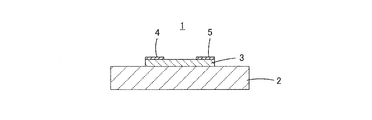
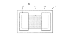
- FIG. 2 is an enlarged sectional view taken along line II-II in FIG. It is a top view which shows the positive temperature coefficient thermistor 11 as a sample produced in the experiment example.
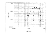
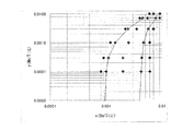
- Table 1 prepared in the experimental example, those containing “Sm” as “Ln” show the relationship between “x (Sm / Ti ratio)” and “z (Na / Al ratio)”.
- FIG. Of the samples shown in Table 2 prepared in the experimental example, those containing “Sm” as “Ln” show the relationship between “x (Sm / Ti ratio)” and “y (Mn / Ti ratio)”.
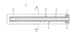
- a positive temperature coefficient thermistor 1 according to an embodiment of the present invention will be described with reference to FIGS.
- the positive temperature coefficient thermistor 1 is in contact with the alumina substrate 2, the thermistor thick film 3 formed on the alumina substrate 2 and exhibiting the PTC characteristic, and the thermistor thick film 3 with at least a part of the thermistor thick film 3 interposed therebetween. And at least one pair of electrodes 4 and 5. Further, although not shown, a protective film may be formed on the alumina substrate 2 so as to cover the thermistor thick film 3 and the electrodes 4 and 5.
- the thermistor thick film 3 is ABO 3 (A always contains barium and may further contain at least one selected from strontium, calcium, lead and rare earth elements. B necessarily contains titanium, and further contains tin, zirconium. , Niobium, tungsten, and antimony may be included.) And a sintered body of a semiconductor ceramic having a barium titanate (BaTiO 3 ) system as a main component.
- ABO 3 A always contains barium and may further contain at least one selected from strontium, calcium, lead and rare earth elements.
- B necessarily contains titanium, and further contains tin, zirconium. , Niobium, tungsten, and antimony may be included.
- This semiconductor ceramic preferably contains at least boron element as a subcomponent. Boron acts to enable low-temperature firing.
- the A content is ⁇ in atomic ratio
- the B content is ⁇ in atomic ratio
- the boron element content Is the atomic ratio ⁇ , 0.05 ⁇ ⁇ / ⁇ ⁇ 1.5, and 1 ⁇ ⁇ / ( ⁇ ) ⁇ 4 It is preferable to satisfy the following condition.
- the boron element contained in the semiconductor ceramic of the present invention exists in the form of an oxide represented by B 2 BaO 4 or B 2 O 3 dissolved in the main component represented by BaTiO 3 ceramic. It may be a thing, and if it contains a boron element, it will not be limited to the said form.
- elements other than boron may be added as subcomponents of the semiconductor ceramic.
- the sintered body of a semiconductor ceramic is x when the total amount of donors contained therein is represented by the donor / Ti atomic ratio, and y when the amount of Mn contained therein is represented by the Mn / Ti atomic ratio.
- the amount of Na in the alumina substrate is expressed as Na / Al atomic ratio, and z, 0.0008 ⁇ (x ⁇ 0.5y ⁇ 0.5z) ⁇ 0.004, 0 ⁇ y ⁇ 0.007, and 0 ⁇ z ⁇ 0.002.
- the resistivity thermistor 1 can achieve a low resistivity of, for example, less than 10 k ⁇ ⁇ cm at room temperature. Furthermore, high adhesion can be obtained between the alumina substrate 2 and the thermistor thick film 3.
- Mn serves as an acceptor for BaTiO 3 -based semiconductor ceramics
- Na also serves as an acceptor like Mn, so that Mn and Na reduce the effect of the donor. It is done. That is, the resistance can be lowered by adding an appropriate amount of donor to the BaTiO 3 based semiconductor ceramic. However, if Na or Mn is present, the effect of the donor is weakened, so that the appropriate amount of donor is shifted to a larger amount. Is shown.
- Na does not exist in the BaTiO 3 -based semiconductor ceramic before firing, and it is intended to be included in the alumina substrate or contained as an impurity. Regarding Na, it is considered that it influences because it diffuses from the alumina substrate into the BaTiO 3 based semiconductor ceramic during firing.
- rare earth elements such as La, Y, Sm, Ce, Dy, Gd and the like shown in JP 2001-326102 A, Nb, Ta, Bi, Sb, W, and the like can be used. .
- the thermistor thick film 3 has a thickness of 1 ⁇ m or more, for example.
- a semiconductor ceramic paste formed by mixing semiconductor ceramic powder with varnish is prepared, and this semiconductor ceramic paste is applied onto the alumina substrate 2 or a doctor blade on the alumina substrate 2. After the method or the like is applied to form a sheet, the firing process may be performed.
- the electrodes 4 and 5 have a portion located on the thermistor thick film 3 as well shown in FIG. As shown well in FIG. 1, the first electrode 4 is formed along the longitudinal direction of the thermistor thick film 3 having a rectangular planar shape. On the other hand, the second electrode 5 is positioned so as to face the first electrode 4 with a predetermined distance from the first electrode 4. Further, the electrodes 4 and 5 respectively form wide lead portions 6 and 7 at respective end portions, and these lead portions 6 and 7 are located on one end side of the insulating ceramic substrate 2. .
- the electrodes 4 and 5 are made of a material capable of making ohmic contact with the thermistor thick film 3.
- a material of the electrodes 4 and 5 for example, a base metal such as Ni, Cu, or Al or an alloy thereof, or ohmic Ag that is ohmicized by addition of a base metal is used.
- a thin film forming method such as sputtering or vapor deposition, or a thick film method in which a conductive paste is applied and baked can be applied.
- the positive temperature coefficient thermistor 1 has a structure in which a thermistor thick film 3 is formed in a long pattern on an elongated alumina substrate 2 (that is, an aspect ratio is large). is doing. Therefore, there is a problem that peeling is likely to occur between the alumina substrate 2 and the thermistor thick film 3 due to differences in the respective linear expansion coefficients.
- high adhesion can be ensured between the alumina substrate 2 and the thermistor thick film 3, and therefore, peeling can be prevented. Accordingly, the present invention becomes more significant particularly when the positive temperature coefficient thermistor has a form in which a long thermistor thick film is formed on a long insulator ceramic substrate as shown in FIG.
- the above prepared powder was pulverized with PSZ balls in water for 5 hours using a ball mill, and then calcined at a temperature of 1000 ° C. for 2 hours.
- MnCO 3 was added to obtain a mixture having the following composition.
- Tables 1 and 2 also show the value of “x ⁇ 0.5y ⁇ 0.5z” for each sample.
- varnish was added to the above mixture to form a paste, which was then applied onto an alumina substrate and fired at a temperature of 1050 ° C. for 2 hours to obtain a thermistor thick film made of a sintered ceramic ceramic.
- the thickness t of the thermistor thick film after firing was 100 ⁇ m.
- a pair of electrodes 14 is formed on the alumina substrate 12 so as to cover each end of the thermistor thick film 13 formed on the alumina substrate 12. And a positive temperature coefficient thermistor 11 as a sample was obtained.
- room temperature resistivity was measured for each of the obtained samples.
- Room temperature resistivity is measured by the two-terminal method when a DC voltage of 1 V is applied at a room temperature of 25 ° C.
- room temperature resistivity when it was 10 k ⁇ ⁇ cm or more, it was determined to be defective.
- the “room temperature resistivity” It was as high as 10 k ⁇ ⁇ cm or more.
- the “room temperature resistivity” is as high as 10 k ⁇ ⁇ cm or more.
- the “room temperature resistivity” is as high as 10 k ⁇ ⁇ cm or more.
- FIG. 4 is a diagram showing the relationship between “x (Sm / Ti ratio)” and “z (Na / Al ratio)” for samples including “Sm” as “Ln” among the samples shown in Table 1. It is.
- FIG. 5 is a diagram showing the relationship between “x (Sm / Ti ratio)” and “y (Mn / Ti ratio)” for samples including “Sm” as “Ln” among the samples shown in Table 2. It is. 4 and 5, it is shown that the area surrounded by the line has a composition within the scope of the present invention.
Landscapes
- Engineering & Computer Science (AREA)
- Microelectronics & Electronic Packaging (AREA)
- Chemical & Material Sciences (AREA)
- Ceramic Engineering (AREA)
- Materials Engineering (AREA)
- Physics & Mathematics (AREA)
- Electromagnetism (AREA)
- Compositions Of Oxide Ceramics (AREA)
- Thermistors And Varistors (AREA)
Abstract
アルミナ基板上に発熱源となるサーミスタ厚膜が形成された形態を有する正特性サーミスタにおいて、低抵抗化を図る。 アルミナ基板(2)と、アルミナ基板(2)上に形成された、PTC特性を示すサーミスタ厚膜(3)と、サーミスタ厚膜(3)の少なくとも一部を挟んで対向する1対の電極(4,5)とを備える、正特性サーミスタ(1)において、サーミスタ厚膜(3)は、チタン酸バリウム系を主成分とする半導体セラミックの焼結体からなり、そこに含まれるドナーの総量をドナー/Ti原子比でxとし、Mn量をMn/Ti原子比でyとし、アルミナ基板(2)中のNa量をNa/Al原子比でzとしたとき、0.0008≦(x-0.5y-0.5z)≦0.004、0≦y≦0.007、および0<z≦0.002の条件を満たすようにする。
Description
この発明は、正特性サーミスタに関するもので、特に、大電流が流れる発熱体としての用途に適した正特性サーミスタに関するものである。
正の抵抗温度特性(PTC特性)を有する半導体セラミックをもって構成されたサーミスタ、すなわち正特性サーミスタは、たとえば発熱体として広く利用されている。正特性サーミスタを利用した発熱体は、自己制御機能を有し、よって外部の制御回路を必要としない点で有利である。
発熱体として用いられる正特性サーミスタは、通常、チタン酸バリウム系半導体粉末を加圧成形した後、焼成することによって得られた、単板形状の半導体セラミックからなる素子本体を備えている。しかし、正特性サーミスタが大面積の発熱体として用いられる場合には、サーミスタ特性を示す半導体セラミックは膜状の形態とされることが好ましい。
このような膜状の発熱源を有する半導体素子としては、たとえば、特開昭55-130101号公報(特許文献1)に記載されたものがある。
特許文献1には、チタン酸バリウム系半導体セラミック粉末に、Ni、Alおよび/またはRuO2粉末とガラスフリットとを加え、有機結合剤を用いてペースト状にした混合物を絶縁性基板上に塗布して厚膜状に成形した後、600~1000℃で焼成することによって得られた、厚膜型正特性半導体素子が記載されている。
しかしながら、特許文献1に記載の厚膜型正特性半導体素子では、チタン酸バリウム系半導体セラミック粉末粒子とNi粉末等の導電性粒子とは、焼結するのではなく、単にガラスで糊付けされた状態にすぎないため、個々の粒子の結合が点接触となり、低抵抗化が困難である。このため、発熱体などに使用される場合において、大電流を通電できず、極めて狭い範囲での実用化しかできない。
事実、特許文献1に記載の実施例では、得られた厚膜型正特性半導体素子の室温における面積抵抗は150~700Ω/cm2の範囲にあり、同文献第3頁左上欄第16~17行の「厚さが0.1mm以下」という文言を根拠に、厚さ0.1mmで計算すると、抵抗率が15kΩ・cm~70kΩ・cmとなり、かなりの高抵抗率となる。ここで、もし、厚みが0.1mmより薄い場合は、さらに高い抵抗率を示すことになる。
なお、特許文献1は、導電性粒子の添加量を変えることによって面積抵抗の制御が可能であることを示唆しているが、良好なPTC特性を維持するため、導電性粒子の添加量の可変範囲は限られている。よって、導電性粒子の添加量を増やすことによる抵抗率の増大はそれほど望めない。
他方、膜状の発熱体ではなく、単板形状の発熱体として用いられる半導体セラミック素子が、たとえば特開平11-246268号公報(特許文献2)に記載されている。
特許文献2には、チタン酸バリウム系の半導体焼結体中に、ホウ素酸化物を含有し、バリウム、ストロンチウム、カルシウム、イットリウム、希土類元素の中から選ばれる少なくとも1種類からなる酸化物を含有しした半導体セラミックであって、ホウ素元素(Bとする)が原子比で、0.005≦B/β≦0.50、1≦B/(α-β)≦4(ただし、α:半導体セラミック中に含まれるバリウム、ストロンチウム、カルシウム、イットリウム、希土類元素の総量;β:半導体セラミック中に含まれるチタン、錫、ジルコニウム、ニオブ、タングステン、アンチモンの総量)となるように添加されている半導体セラミックが開示されている。
特許文献2には、また、1000℃以下の温度で焼成して得られた単板形状の半導体セラミック素子が開示されている。
しかしながら、特許文献2では、単板形状の半導体セラミック素子が開示されているのみで、膜状の発熱体については一切開示されていない。すなわち、特許文献2では、アルミナ基板などの絶縁体セラミック基板上に発熱体となる厚膜を形成した後、この厚膜を焼結できるかどうかは実証されていない。また、半導体セラミックを絶縁体セラミック基板上において厚膜状態で焼成したとき、焼結体としての厚膜が低抵抗となり得るか、あるいは、絶縁体セラミック基板との間で剥離等が生じず、高い密着性を確保できるか、など、さらに追求すべき課題がある。
そこで、この発明の目的は、絶縁体セラミック基板上に発熱源となる厚膜が形成された形態を有しながら、低抵抗化が図られ、よって大電流の通電が可能であり、しかも絶縁体セラミック基板と厚膜との間での密着性に優れた、正特性サーミスタを提供しようとすることである。
この発明では、絶縁体セラミック基板として、アルミナ基板が用いられる。
そして、本件発明者は、アルミナ基板中のナトリウム量、ならびにチタン酸バリウム系半導体セラミック中のドナー量およびマンガン量が一定の関係を示す場合に低抵抗を実現できることを見出し、この発明をなすに至ったものである。
この発明に係る正特性サーミスタは、アルミナ基板と、アルミナ基板上に形成された、正の抵抗温度特性を示すサーミスタ厚膜と、サーミスタ厚膜に接し、かつサーミスタ厚膜の少なくとも一部を挟んで対向する、少なくとも1対の電極とを備えるものであるが、上述した技術的課題を解決するため、次のような構成を備えることを特徴としている。
上記サーミスタ厚膜は、チタン酸バリウム系を主成分とする半導体セラミックの焼結体からなることを特徴としている。
そして、半導体セラミックの焼結体に含まれるドナーの総量を、ドナー/Ti原子比で表わしたとき、xとし、半導体セラミックの焼結体に含まれるMn量を、Mn/Ti原子比で表わしたとき、yとし、アルミナ基板中のNa量を、Na/Al原子比で表わしたとき、zとしたとき、
0.0008≦(x-0.5y-0.5z)≦0.004、
0≦y≦0.007、および
0<z≦0.002
の条件を満たすことをさらなる特徴としている。
0.0008≦(x-0.5y-0.5z)≦0.004、
0≦y≦0.007、および
0<z≦0.002
の条件を満たすことをさらなる特徴としている。
上記半導体セラミックは、副成分として少なくともホウ素元素を含むことが好ましい。
上記ドナーは、好ましくは、希土類元素である。
この発明によれば、アルミナ基板中のNa量、ならびにチタン酸バリウム系半導体セラミック中のドナー量およびMn量が上述のような関係に選ばれているので、後述する実験例によって明らかにされるように、低抵抗化が図られた正特性サーミスタを得ることができる。
また、サーミスタ厚膜を構成する半導体セラミックは、焼結により、結晶粒子同士が面接触した状態となっているので、粒子間の接触面積を広くすることができる。このことも、低抵抗化に寄与する。すなわち、前述の特許文献1に記載のもののように、半導体粉末粒子および導電性粒子が点接触するように単に糊付けされているような状態のものに比べて、低抵抗化を図ることができる。
さらに、この発明によれば、アルミナ基板とサーミスタ厚膜との間で高い密着性を得ることができ、よって剥離等の問題を招きにくくすることができる。
この発明において、サーミスタ厚膜を構成する半導体セラミックが、副成分として少なくともホウ素元素を含んでいると、1000℃程度またはそれより低い温度で確実に焼結させることができる。よって、半導体セラミック焼結体からなるサーミスタ厚膜をアルミナ基板上に形成した構造、すなわち大電流用の発熱体として適した形態の正特性サーミスタを容易に実現することができる。
図1および図2を参照して、この発明の一実施形態による正特性サーミスタ1について説明する。
正特性サーミスタ1は、アルミナ基板2と、アルミナ基板2上に形成された、PTC特性を示すサーミスタ厚膜3と、サーミスタ厚膜3に接し、かつサーミスタ厚膜3の少なくとも一部を挟んで対向する、少なくとも1対の電極4および5とを備えている。さらに、図示しないが、アルミナ基板2上には、サーミスタ厚膜3ならびに電極4および5を覆うように、保護膜が形成されてもよい。
サーミスタ厚膜3は、ABO3(Aは、バリウムを必ず含み、さらにストロンチウム、カルシウム、鉛および希土類元素から選ばれる少なくとも1種を含むことがある。Bは、チタンを必ず含み、さらに錫、ジルコニウム、ニオブ、タングステンおよびアンチモンから選ばれる少なくとも1種を含むことがある。)で表わされるチタン酸バリウム(BaTiO3)系を主成分とする半導体セラミックの焼結体からなる。
この半導体セラミックは、副成分として少なくともホウ素元素を含むことが好ましい。ホウ素は、低温焼成を可能とするように作用するものであるが、半導体セラミックにおける、上記Aの含有量を原子比でα、上記Bの含有量を原子比でβ、およびホウ素元素の含有量を原子比でγとしたとき、
0.05≦γ/β≦1.5、および
1≦γ/(α-β)≦4
の条件を満たすようにされることが好ましい。
0.05≦γ/β≦1.5、および
1≦γ/(α-β)≦4
の条件を満たすようにされることが好ましい。
この発明の半導体セラミックに含まれるホウ素元素は、BaTiO3系セラミックで表わされる主成分に固溶しているもの、B2BaO4あるいはB2O3で示される酸化物の状態で存在しているものであってもよく、ホウ素元素を含有していれば、上記形態に限定されるものではない。
なお、低温焼成を可能とするため、ホウ素以外の元素が半導体セラミックの副成分として添加されてもよい。
半導体セラミックの焼結体は、そこに含まれるドナーの総量を、ドナー/Ti原子比で表わしたとき、xとし、そこに含まれるMn量を、Mn/Ti原子比で表わしたとき、yとし、アルミナ基板中のNa量を、Na/Al原子比で表わしたとき、zとしたとき、
0.0008≦(x-0.5y-0.5z)≦0.004、
0≦y≦0.007、および
0<z≦0.002
の条件を満たすようにされる。
0.0008≦(x-0.5y-0.5z)≦0.004、
0≦y≦0.007、および
0<z≦0.002
の条件を満たすようにされる。
上記の条件を満たすことによって、正特性サーミスタ1において、室温でたとえば10kΩ・cm未満といった低い抵抗率を実現することができる。さらに、アルミナ基板2とサーミスタ厚膜3との間で高い密着性を得ることができる。
上記(x-0.5y-0.5z)の値が0.0008未満では、BaTiO3系半導体セラミックの抵抗率が高くなり、他方、0.004を超えても、同様に高抵抗率となる。
これは、BaTiO3系半導体セラミックに対して、Mnがアクセプタとなり、また、Naも、Mnと同様、アクセプタ的な役割を果たすので、これらMnおよびNaがドナーの効果を減殺するためであると考えられる。すなわち、BaTiO3系半導体セラミックに適量のドナーを添加することで低抵抗化が可能であるが、NaやMnが存在すると、ドナーの効果を弱めるため、ドナーの適量がより多い方へシフトすることを示している。
なお、Naに関しては、焼成前にはBaTiO3系半導体セラミック中には存在せず、アルミナ基板に敢えて含有したものも、不純物として含有するものも対象となる。Naに関しては、焼成中にアルミナ基板からBaTiO3系半導体セラミック中に拡散するために影響するものと考える。
また、Mn量に相当するyが0.007を超え、あるいは、Na量に相当するzが0.002を超えると、ドナー量をより多くするだけでは補正しきれなくなり、ドナー量によらず高抵抗化してしまう。なお、Mnについては、含有されないこともある。
ドナー元素としては、特開2001-326102号公報などで示されているLa、Y、Sm、Ce、Dy、Gdなどの希土類元素や、Nb、Ta、Bi、Sb、Wなどを用いることができる。
サーミスタ厚膜3は、たとえば1μm以上の厚みを有している。サーミスタ厚膜3を形成するため、たとえば、半導体セラミック粉末にワニスを混合して形成した半導体セラミックペーストを用意し、この半導体セラミックペーストをアルミナ基板2上に塗布するか、アルミナ基板2上でドクターブレード法等を適用してシート状に成形するかした後、焼成工程を実施するようにすればよい。
電極4および5は、図2によく示されているように、サーミスタ厚膜3上に位置する部分を有している。第1の電極4は、図1によく示されているように、矩形の平面形状を有するサーミスタ厚膜3の長手方向に沿うように形成されている。他方、第2の電極5は、第1の電極4に対して所定の間隔を隔てながら、第1の電極4に対向するように位置している。また、電極4および5は、それぞれ、各々の端部において幅広の引出し部6および7を形成しており、これら引出し部6および7は、絶縁体セラミック基板2の一方端側に位置している。
電極4および5は、サーミスタ厚膜3との間でオーミック接触が取れる材料から構成される。電極4および5の材料としては、たとえば、Ni、Cu、Al等の卑金属またはその合金、あるいは卑金属添加によりオーミック化されたオーミックAg等が用いられる。
電極4および5を形成するにあたっては、たとえば、スパッタリング、蒸着等の薄膜形成法、または導電性ペーストを塗布して焼き付ける厚膜法を適用することができる。
図示した正特性サーミスタ1は、特に図1からわかるように、長尺状の(すなわち、アスペクト比が大きい)アルミナ基板2上にサーミスタ厚膜3が長尺状のパターンをもって形成された構造を有している。そのため、アルミナ基板2とサーミスタ厚膜3との間で、各々の線膨張係数の違い等が原因となって剥がれが生じやすいという課題がある。しかし、この発明によれば、アルミナ基板2とサーミスタ厚膜3との間で高い密着性を確保でき、よって、剥がれが生じにくくすることができる。したがって、この発明は、特に、正特性サーミスタが図1に示すような長尺の絶縁体セラミック基板上に長尺のサーミスタ厚膜が形成された形態を有するとき、より意義深いものとなる。
次に、この発明の効果を確認するために実施した実験例について説明する。
[実験例1]
まず、BaCO3、TiO2、ならびに、ドナーとなる希土類元素酸化物:Ln2O3としてのSm2O3、Y2O3およびNd2O3の各粉末を用意し、これら粉末を(Ba1-xLnx)TiO3となるように調合した。ここで、xは、ドナーの総量をドナー/Ti原子比で表わしたものであるが、表1および表2の「x」の欄に示されている。
まず、BaCO3、TiO2、ならびに、ドナーとなる希土類元素酸化物:Ln2O3としてのSm2O3、Y2O3およびNd2O3の各粉末を用意し、これら粉末を(Ba1-xLnx)TiO3となるように調合した。ここで、xは、ドナーの総量をドナー/Ti原子比で表わしたものであるが、表1および表2の「x」の欄に示されている。
次いで、上記調合粉末を、ボールミルを用いて、水中でPSZボールとともに5時間粉砕した後、1000℃の温度で2時間仮焼した。得られた仮焼粉に、BNとBaCO3とを添加するとともに、表1および表2の「y」(Mn量を、Mn/Ti原子比で表わしたもの)の欄に示す添加量をもって、MnCO3を添加して、以下の組成のような混合物を得た。
(Ba1-xLnx)TiO3+0.3BN+0.15BaCO3+yMnCO3
他方、表1および表2の「z」(アルミナ基板中のNa量をNa/Al原子比で表わしたもの)となるNa量を有するアルミナ基板を用意した。
他方、表1および表2の「z」(アルミナ基板中のNa量をNa/Al原子比で表わしたもの)となるNa量を有するアルミナ基板を用意した。
表1および表2には、各試料についての「x-0.5y-0.5z」の値も示されている。
次に、上記混合物にワニスを添加し、ペースト化した後、アルミナ基板上に塗布して1050℃の温度で2時間焼成して、半導体セラミックの焼結体からなるサーミスタ厚膜を得た。焼成後のサーミスタ厚膜の厚みtは100μmであった。
次に、Niスパッタリングを実施することによって、図3に示すように、アルミナ基板12上に形成された上記サーミスタ厚膜13の各端部を覆う状態で、アルミナ基板12上に1対の電極14および15を形成し、試料となる正特性サーミスタ11を得た。
次に、表1および表2に示すように、得られた各試料について、「室温抵抗率」を測定した。「室温抵抗率」は、室温25℃において、1Vの直流電圧を印加した際の抵抗率を2端子法で測定したものである。この「室温抵抗率」に関して、10kΩ・cm以上の場合、不良と判定した。

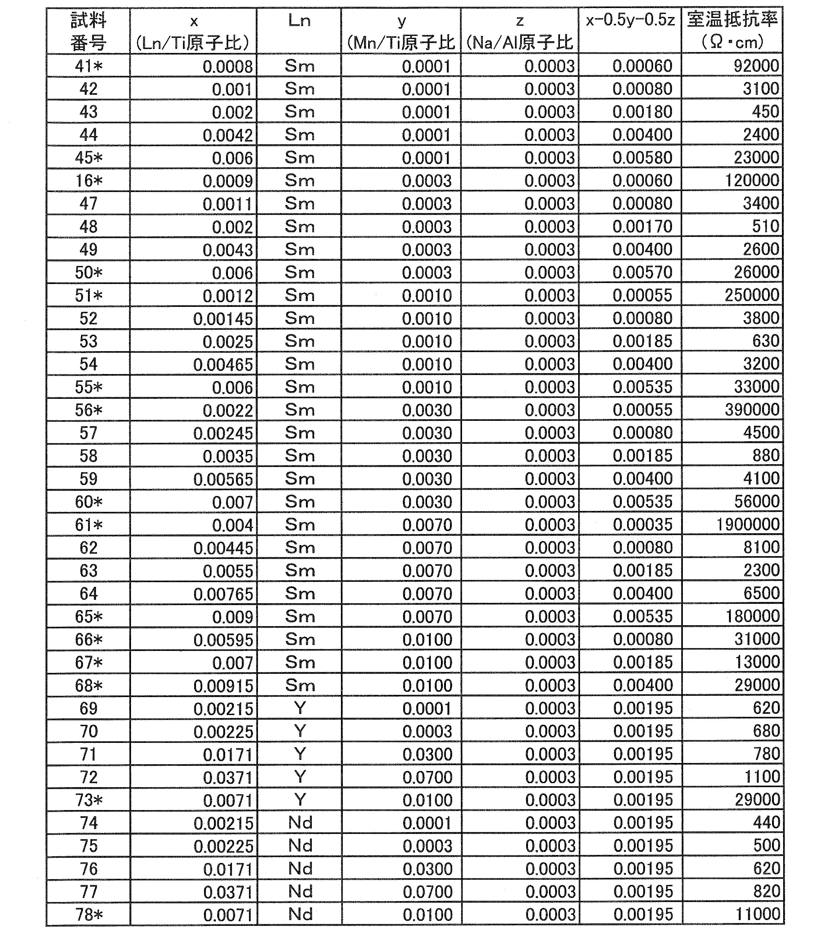
表1および表2において、試料番号に*を付したものは、この発明の範囲外の比較例である。なお、表1に示した試料と表2に示した試料とは、前者が半導体セラミック中にMnを含まず、後者がMnを含む点で区別される。
表1および表2に示すように、この発明の範囲内の試料2~4、7~9、12~14、17~19、22~24、29~33、35~39、42~44、47~49、52~54、57~59、62~64、69~72、および74~77によれば、「室温抵抗率」を10kΩ・cm未満と低くすることができる。これらの試料は、0.0008≦(x-0.5y-0.5z)≦0.004、0≦y≦0.007、および0<z≦0.002の条件を満たしている。
また、上記のこの発明の範囲内の試料については、表1および表2には示されていないが、サーミスタ厚膜がアルミナ基板から剥がれることもなかった。
これらに対して、「x-0.5y-0.5z」の値が0.0008未満の試料1、6、11、16、21、41、46、51、56および61では、「室温抵抗率」が10kΩ・cm以上と高くなった。
同様に、「x-0.5y-0.5z」の値が0.004を超える試料5、10、15、20、25、45、50、55、60および65でも、「室温抵抗率」が10kΩ・cm以上と高くなった。
また、「y」が0.007を超える試料66~68、73および78でも、「室温抵抗率」が10kΩ・cm以上と高くなった。
また、「z」が0.002を超える試料26~28、34、40でも、「室温抵抗率」が10kΩ・cm以上と高くなった。
図4は、表1に示した試料のうち、「Ln」として「Sm」を含むものについて、「x(Sm/Ti比)」と「z(Na/Al比)」との関係を示す図である。図5は、表2に示した試料のうち、「Ln」として「Sm」を含むものについて、「x(Sm/Ti比)」と「y(Mn/Ti比)」との関係を示す図である。図4および図5において、線で囲まれた領域がこの発明の範囲内の組成であることを示している。
1,11 正特性サーミスタ
2,12 アルミナ基板
3,13 サーミスタ厚膜
4,5,14,15 電極
2,12 アルミナ基板
3,13 サーミスタ厚膜
4,5,14,15 電極
Claims (3)
- アルミナ基板と、
前記アルミナ基板上に形成された、正の抵抗温度特性を示すサーミスタ厚膜と、
前記サーミスタ厚膜に接し、かつ前記サーミスタ厚膜の少なくとも一部を挟んで対向する、少なくとも1対の電極と
を備え、
前記サーミスタ厚膜は、チタン酸バリウム系を主成分とする半導体セラミックの焼結体からなり、
前記半導体セラミックの焼結体に含まれるドナーの総量を、ドナー/Ti原子比で表わしたとき、xとし、前記半導体セラミックの焼結体に含まれるMn量を、Mn/Ti原子比で表わしたとき、yとし、前記アルミナ基板中のNa量を、Na/Al原子比で表わしたとき、zとしたとき、
0.0008≦(x-0.5y-0.5z)≦0.004、
0≦y≦0.007、および
0<z≦0.002
の条件を満たす、
正特性サーミスタ。 - 前記半導体セラミックは、副成分として少なくともホウ素元素を含む、請求項1に記載の正特性サーミスタ。
- 前記ドナーは希土類元素である、請求項1または2に記載の正特性サーミスタ。
Applications Claiming Priority (2)
| Application Number | Priority Date | Filing Date | Title |
|---|---|---|---|
| JP2011-031570 | 2011-02-17 | ||
| JP2011031570 | 2011-02-17 |
Publications (1)
| Publication Number | Publication Date |
|---|---|
| WO2012111385A1 true WO2012111385A1 (ja) | 2012-08-23 |
Family
ID=46672324
Family Applications (1)
| Application Number | Title | Priority Date | Filing Date |
|---|---|---|---|
| PCT/JP2012/051331 Ceased WO2012111385A1 (ja) | 2011-02-17 | 2012-01-23 | 正特性サーミスタ |
Country Status (1)
| Country | Link |
|---|---|
| WO (1) | WO2012111385A1 (ja) |
Cited By (3)
| Publication number | Priority date | Publication date | Assignee | Title |
|---|---|---|---|---|
| DE102017101946A1 (de) | 2017-02-01 | 2018-08-02 | Epcos Ag | PTC-Heizer mit verringertem Einschaltstrom |
| CN116315439A (zh) * | 2022-12-05 | 2023-06-23 | 欣旺达电动汽车电池有限公司 | 一种隔膜、钠离子电池和用电设备 |
| EP4297052A4 (en) * | 2021-01-13 | 2025-12-03 | Jiangsu New Linzhi Electronic Tech Co Ltd | A ceramic thermistor element with a positive temperature coefficient, exhibiting high resistance to reducing atmospheres, and its preparation process. |
Citations (4)
| Publication number | Priority date | Publication date | Assignee | Title |
|---|---|---|---|---|
| JPS55130101A (en) * | 1979-03-30 | 1980-10-08 | Tokyo Shibaura Electric Co | Method of manufacting thick film positive temperature coefficient semiconductor element |
| JPH11246268A (ja) * | 1998-03-05 | 1999-09-14 | Murata Mfg Co Ltd | 半導体セラミックおよび半導体セラミック素子 |
| JP2002076609A (ja) * | 2000-08-25 | 2002-03-15 | Kyocera Corp | 回路基板 |
| JP2008169453A (ja) * | 2007-01-15 | 2008-07-24 | Dowa Electronics Materials Co Ltd | 銀粒子分散液およびその製造方法 |
-
2012
- 2012-01-23 WO PCT/JP2012/051331 patent/WO2012111385A1/ja not_active Ceased
Patent Citations (4)
| Publication number | Priority date | Publication date | Assignee | Title |
|---|---|---|---|---|
| JPS55130101A (en) * | 1979-03-30 | 1980-10-08 | Tokyo Shibaura Electric Co | Method of manufacting thick film positive temperature coefficient semiconductor element |
| JPH11246268A (ja) * | 1998-03-05 | 1999-09-14 | Murata Mfg Co Ltd | 半導体セラミックおよび半導体セラミック素子 |
| JP2002076609A (ja) * | 2000-08-25 | 2002-03-15 | Kyocera Corp | 回路基板 |
| JP2008169453A (ja) * | 2007-01-15 | 2008-07-24 | Dowa Electronics Materials Co Ltd | 銀粒子分散液およびその製造方法 |
Cited By (4)
| Publication number | Priority date | Publication date | Assignee | Title |
|---|---|---|---|---|
| DE102017101946A1 (de) | 2017-02-01 | 2018-08-02 | Epcos Ag | PTC-Heizer mit verringertem Einschaltstrom |
| US12424357B2 (en) | 2017-02-01 | 2025-09-23 | Tdk Electronics Ag | PTC heater with reduced switch-on current |
| EP4297052A4 (en) * | 2021-01-13 | 2025-12-03 | Jiangsu New Linzhi Electronic Tech Co Ltd | A ceramic thermistor element with a positive temperature coefficient, exhibiting high resistance to reducing atmospheres, and its preparation process. |
| CN116315439A (zh) * | 2022-12-05 | 2023-06-23 | 欣旺达电动汽车电池有限公司 | 一种隔膜、钠离子电池和用电设备 |
Similar Documents
| Publication | Publication Date | Title |
|---|---|---|
| JP5099011B2 (ja) | チタン酸バリウム系半導体磁器組成物とそれを用いたptc素子 | |
| JP5327556B2 (ja) | 半導体セラミック及び正特性サーミスタ | |
| US9666369B2 (en) | Dielectric ceramic composition and multilayer ceramic capacitor containing the same | |
| JP6424728B2 (ja) | 半導体磁器組成物およびptcサーミスタ | |
| JP6915222B2 (ja) | 誘電体組成物及びそれを含む積層セラミックキャパシター | |
| US9530547B2 (en) | Laminated PTC thermistor element | |
| JP2002246207A (ja) | 電圧非直線抵抗体及び磁器組成物 | |
| US9799451B2 (en) | Dielectric composition and multilayer ceramic capacitor containing the same | |
| JP2017034140A (ja) | 半導体磁器組成物およびptcサーミスタ | |
| JP6102405B2 (ja) | 誘電体磁器組成物、および誘電体素子 | |
| WO2012111385A1 (ja) | 正特性サーミスタ | |
| CN110797189B (zh) | 多层陶瓷电容器 | |
| JP2021068734A (ja) | セラミック電子部品およびその製造方法 | |
| JP7700195B2 (ja) | セラミックデバイスおよびその製造方法 | |
| US20140247107A1 (en) | Barium titanate semiconductor ceramic and ptc thermistor using the same | |
| JP4710096B2 (ja) | 積層型正特性サーミスタ | |
| JP4792900B2 (ja) | バリスタ用磁器組成物、及び積層バリスタ | |
| US8390421B2 (en) | Semiconductor ceramic and positive-coefficient characteristic thermistor | |
| WO2012111386A1 (ja) | 正特性サーミスタ | |
| JPH11340090A (ja) | 粒界絶縁型積層セラミックコンデンサの製造方法 | |
| JP2014072374A (ja) | チタン酸バリウム系半導体磁器組成物およびそれを用いたptcサーミスタ | |
| WO2013065373A1 (ja) | 半導体セラミックおよびそれを用いたptcサーミスタ | |
| JPH04115409A (ja) | 非還元性誘電体磁器組成物 | |
| WO2010110331A1 (ja) | 半導体磁器組成物、発熱体及び発熱モジュール | |
| JP4788274B2 (ja) | Ctr特性を有する酸化物導電体磁器および抵抗体 |
Legal Events
| Date | Code | Title | Description |
|---|---|---|---|
| 121 | Ep: the epo has been informed by wipo that ep was designated in this application |
Ref document number: 12746575 Country of ref document: EP Kind code of ref document: A1 |
|
| NENP | Non-entry into the national phase |
Ref country code: DE |
|
| 122 | Ep: pct application non-entry in european phase |
Ref document number: 12746575 Country of ref document: EP Kind code of ref document: A1 |
|
| NENP | Non-entry into the national phase |
Ref country code: JP |