WO2012108290A1 - 導電性ペースト及び該導電性ペーストを用いた太陽電池素子 - Google Patents
導電性ペースト及び該導電性ペーストを用いた太陽電池素子 Download PDFInfo
- Publication number
- WO2012108290A1 WO2012108290A1 PCT/JP2012/052055 JP2012052055W WO2012108290A1 WO 2012108290 A1 WO2012108290 A1 WO 2012108290A1 JP 2012052055 W JP2012052055 W JP 2012052055W WO 2012108290 A1 WO2012108290 A1 WO 2012108290A1
- Authority
- WO
- WIPO (PCT)
- Prior art keywords
- conductive paste
- glass
- glass frit
- solar cell
- semiconductor silicon
- Prior art date
- Legal status (The legal status is an assumption and is not a legal conclusion. Google has not performed a legal analysis and makes no representation as to the accuracy of the status listed.)
- Ceased
Links
Images
Classifications
-
- H—ELECTRICITY
- H10—SEMICONDUCTOR DEVICES; ELECTRIC SOLID-STATE DEVICES NOT OTHERWISE PROVIDED FOR
- H10F—INORGANIC SEMICONDUCTOR DEVICES SENSITIVE TO INFRARED RADIATION, LIGHT, ELECTROMAGNETIC RADIATION OF SHORTER WAVELENGTH OR CORPUSCULAR RADIATION
- H10F77/00—Constructional details of devices covered by this subclass
- H10F77/20—Electrodes
- H10F77/206—Electrodes for devices having potential barriers
- H10F77/211—Electrodes for devices having potential barriers for photovoltaic cells
-
- H—ELECTRICITY
- H10—SEMICONDUCTOR DEVICES; ELECTRIC SOLID-STATE DEVICES NOT OTHERWISE PROVIDED FOR
- H10F—INORGANIC SEMICONDUCTOR DEVICES SENSITIVE TO INFRARED RADIATION, LIGHT, ELECTROMAGNETIC RADIATION OF SHORTER WAVELENGTH OR CORPUSCULAR RADIATION
- H10F19/00—Integrated devices, or assemblies of multiple devices, comprising at least one photovoltaic cell covered by group H10F10/00, e.g. photovoltaic modules
-
- H—ELECTRICITY
- H01—ELECTRIC ELEMENTS
- H01B—CABLES; CONDUCTORS; INSULATORS; SELECTION OF MATERIALS FOR THEIR CONDUCTIVE, INSULATING OR DIELECTRIC PROPERTIES
- H01B1/00—Conductors or conductive bodies characterised by the conductive materials; Selection of materials as conductors
- H01B1/20—Conductive material dispersed in non-conductive organic material
- H01B1/22—Conductive material dispersed in non-conductive organic material the conductive material comprising metals or alloys
-
- Y—GENERAL TAGGING OF NEW TECHNOLOGICAL DEVELOPMENTS; GENERAL TAGGING OF CROSS-SECTIONAL TECHNOLOGIES SPANNING OVER SEVERAL SECTIONS OF THE IPC; TECHNICAL SUBJECTS COVERED BY FORMER USPC CROSS-REFERENCE ART COLLECTIONS [XRACs] AND DIGESTS
- Y02—TECHNOLOGIES OR APPLICATIONS FOR MITIGATION OR ADAPTATION AGAINST CLIMATE CHANGE
- Y02E—REDUCTION OF GREENHOUSE GAS [GHG] EMISSIONS, RELATED TO ENERGY GENERATION, TRANSMISSION OR DISTRIBUTION
- Y02E10/00—Energy generation through renewable energy sources
- Y02E10/50—Photovoltaic [PV] energy
- Y02E10/547—Monocrystalline silicon PV cells
Definitions
- the present invention relates to a lead-free conductive paste that can be used as an electrode formed in a semiconductor silicon solar cell.
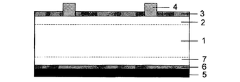
- the solar cell element As an electronic component using a semiconductor silicon substrate, a solar cell element as shown in FIG. 1 is known. As shown in FIG. 1, the solar cell element is formed by forming an n-type semiconductor silicon layer 2 on the light-receiving surface side of a p-type semiconductor silicon substrate 1 having a thickness of about 200 ⁇ m, and nitriding to increase the light-receiving efficiency on the light-receiving surface side surface.
- An antireflection film 3 such as a silicon film, and a surface electrode 4 connected to the semiconductor are formed on the antireflection film 3.
- an aluminum electrode layer 5 is uniformly formed on the back side of the p-type semiconductor silicon substrate 1.
- the aluminum electrode layer 5 is generally formed by applying an aluminum paste material composed of an aluminum powder, glass frit, an organic vehicle containing a binder such as ethyl cellulose or acrylic resin by screen printing or the like, and having a temperature of about 600 to 900 ° C. It is formed by baking for a short time.
- the glass frit containing the lead component described above can be used for a conductive paste such as an aluminum paste material to obtain a high BSF effect, and is an important component for lowering the melting point of the conductive paste. However, it has a great negative effect on the human body and the environment.
- Patent Document 1 and Patent Document 2 described above have a problem that the conductive paste contains a lead component.
- an object of the present invention is to obtain a lead-free conductive paste that can be used as an electrode formed in a semiconductor silicon solar cell.
- the present invention relates to a conductive paste for a solar cell using a semiconductor silicon substrate, and the composition of the glass frit contained in the conductive paste is substantially free of a lead component and contains 1 to 2 SiO 2 by mass%. 20, 5 to 30 for B 2 O 3 , 0 to 10 for Al 2 O 3 , 5 to 35 for ZnO, 5 for RO (total of at least one selected from the group consisting of MgO, CaO, SrO, and BaO) 30 to 30, R 2 O (total of at least one selected from the group consisting of Li 2 O, Na 2 O, and K 2 O) 0.1 to 6 and Bi 2 O 3 to 10 to 60
- the conductive paste is characterized.
- the surface resistance of the p + layer is about 20 to 30 ⁇ / ⁇ , so that the p + layer when the conductive paste of the present invention is used.
- the surface resistance is preferably 30 ⁇ / ⁇ or less. When the surface resistance is lower, conversion efficiency is improved when used as a solar cell element.
- the glass frit of the present invention is characterized in that the thermal expansion coefficient at 30 ° C. to 300 ° C. is (70 to 110) ⁇ 10 ⁇ 7 / ° C. and the softening point is 450 ° C. or higher and 600 ° C. or lower.
- the above thermal expansion coefficient means a linear expansion coefficient.
- the conductive paste of the present invention is an aluminum paste material having aluminum powder.
- the conductive paste of the present invention is characterized in that the composition of the glass frit contains at least K 2 O as R 2 O.
- the conductive paste of the present invention is characterized in that the composition of the glass frit contains at least BaO as RO.
- the present invention it is possible to obtain a conductive paste containing glass frit that does not contain lead.
- the conductive paste of the present invention as a solar cell element, a high BSF effect can be obtained. Also, good adhesion to the semiconductor silicon substrate can be obtained. Furthermore, since it does not substantially contain a lead component, there is no harmful effect on the human body and the environment.
- the conductive paste of the present invention contains glass frit (1 to 5% by mass) in addition to an organic vehicle containing aluminum powder and a binder such as ethyl cellulose or acrylic resin, and the glass frit is substantially free of a lead component.
- a binder such as ethyl cellulose or acrylic resin
- R 2 O total of at least one selected from the group consisting of Li 2 O, Na 2 O, and K 2 O
- Bi 2 O 3 is an electrically conductive paste characterized by containing 10-60.
- SiO 2 is a glass forming component.
- B 2 O 3 which is another glass forming component, a stable glass can be formed, and 1 to 20% ( (The same applies to the mass% below). If it exceeds 20%, the softening point of the glass will rise, making it difficult to use as a conductive paste. More preferably, it is 5 to 17%, and further preferably 8 to 15%.
- B 2 O 3 is a glass-forming component, facilitates glass melting, suppresses an excessive increase in the thermal expansion coefficient of glass, imparts fluidity to glass during firing, and lowers the dielectric constant of glass. And 5 to 30% in the glass. If it is less than 5, the fluidity of the glass becomes insufficient and the sinterability is impaired. On the other hand, if it exceeds 30%, the stability of the glass decreases. Further, it is more preferably in the range of 10 to 25%, still more preferably 15 to 25%.
- Al 2 O 3 is an optional component that suppresses crystallization of glass. If it exceeds 10%, the softening point of the glass rises, making it difficult to use as a conductive paste. More preferably, it may be 0 to 5%.
- ZnO is a component that lowers the softening point of glass and is contained in the glass in an amount of 5 to 35%. If it is less than 5%, the above-mentioned action cannot be exhibited. If it exceeds 35%, the glass becomes unstable and crystals are likely to be formed. Further, it is more preferably in the range of 8-30%, still more preferably 10-20%.
- RO total of at least one selected from the group consisting of MgO, CaO, SrO and BaO
- RO lowers the softening point of the glass and is contained in the glass in an amount of 5 to 30%. If it is less than 5%, the softening point of the glass is not sufficiently lowered and the sinterability is impaired. On the other hand, if it exceeds 30%, the thermal expansion coefficient of the glass may become too high.
- the range is preferably 10 to 30%, more preferably 10 to 20%.
- RO may be a single component or a mixture of a plurality of components, but more preferably contains BaO.
- R 2 O (total of at least one selected from the group consisting of Li 2 O, Na 2 O, and K 2 O) lowers the softening point of the glass and adjusts the thermal expansion coefficient to an appropriate range. It is contained in the range of 1 to 6%. If it is less than 0.1%, the softening point of the glass is not sufficiently lowered and the sinterability is impaired. On the other hand, if it exceeds 6%, the thermal expansion coefficient may be excessively increased. More preferably, it is in the range of 1 to 6%, more preferably 1 to 3%.
- the surface resistance of the p + layer can be made lower than 30 ⁇ / ⁇ , but the R 2 O exceeds 6% by mass. If containing Te, the order by R 2 O alkali component increases sometimes exhibit deliquescence, in the present invention to 6% by mass or less the R 2 O.
- R 2 O may be a single component or a mixture of a plurality of components.
- the “main component” mentioned above may be such that the mass of K 2 O with respect to the total mass of R 2 O components is 50% by mass or more, and preferably 70% by mass or more.
- Bi 2 O 3 lowers the softening point of the glass and adjusts the thermal expansion coefficient, and is contained in the range of 10 to 60%. If it is less than 10%, the softening point of the glass is not sufficiently lowered, and the sinterability is impaired. On the other hand, if it exceeds 60%, the thermal expansion coefficient is excessively increased. More preferably, it is in the range of 15 to 55%.
- CuO, TiO 2 , In 2 O 3 , SnO 2 , TeO 2 or the like represented by a general oxide may be added.
- substantially not containing lead hereinafter sometimes referred to as PbO
- substantially free of PbO means an amount of PbO mixed as an impurity in the glass raw material. For example, if it is in the range of 0.3% or less in the low-melting glass, there is almost no influence on the adverse effects described above, that is, the influence on the human body and the environment, the insulation characteristics, etc., and it is not substantially affected by PbO. Become.
- the glass frit By using the glass frit, it is possible to obtain a conductive paste having a thermal expansion coefficient of (70 to 110) ⁇ 10 ⁇ 7 / ° C. and a softening point of 450 to 600 ° C. at 30 to 300 ° C. .
- the coefficient of thermal expansion is outside (70 to 110) ⁇ 10 ⁇ 7 / ° C., problems such as peeling and substrate warpage occur during electrode formation.
- it is in the range of (75-100) ⁇ 10 ⁇ 7 / ° C.
- the softening point exceeds 600 ° C., it does not flow sufficiently at the time of firing, so that problems such as poor adhesion to the semiconductor silicon substrate occur.
- the softening point is preferably 480 ° C or higher and 580 ° C or lower.
- the conductive paste of the present invention can be used for solar cell elements as described above. Furthermore, since the conductive paste can be baked at a low temperature, it can be used as a substrate for electronic materials such as a wiring pattern forming material using silver or aluminum or various electrodes.
- One of the preferred embodiments of the conductive paste of the present invention is a conductive paste containing glass frit, aluminum powder, and an organic vehicle, and the viscosity of the conductive paste is preferably 200 Pa ⁇ s or less.
- the conductive paste is applied and fired on a semiconductor silicon substrate to form an aluminum electrode layer. If the viscosity is out of the above range, the moldability and workability may be deteriorated.
- the particle size of the glass frit contained in the conductor paste is preferably 1 to 10 ⁇ m in average particle size and 30 ⁇ m or less in maximum particle size.
- the particle size of the glass frit was measured using a laser diffraction / scattering soot particle size / particle size distribution measuring device (manufactured by Nikkiso Co., Ltd.). If the average particle diameter of the glass frit exceeds 10 ⁇ m and the maximum particle diameter exceeds 30 ⁇ m, the adhesion between the semiconductor silicon substrate and the aluminum electrode layer may be reduced when the aluminum electrode layer is formed on the semiconductor silicon substrate. .
- the aluminum powder has conductivity, and in order to exhibit conductivity usable as an aluminum electrode layer, it is preferable to have 50 to 80% by mass with respect to the conductive paste.
- the organic vehicle is composed of an organic solvent and a binder, and volatilizes when fired to form an aluminum electrode layer.
- the viscosity of the organic solvent and the binder may be adjusted as appropriate so that the viscosity is in the above-described range and volatilizes during the baking process. %, And the binder may be contained in an amount of 1 to 10% by mass.
- Organic solvents include, for example, N, N′-dimethylformamide (DMF), ⁇ -terpineol, higher alcohol, ⁇ -butyllactone ( ⁇ -BL), tetralin, butyl carbitol acetate, ethyl acetate, isoamyl acetate, diethylene glycol monoethyl Ether, diethylene glycol monoethyl ether acetate, benzyl alcohol, toluene, 3-methoxy-3-methylbutanol, triethylene glycol monomethyl ether, triethylene glycol dimethyl ether, dipropylene glycol monomethyl ether, dipropylene glycol monobutyl ether, tripropylene glycol monomethyl ether , Tripropylene glycol monobutyl ether, propylene carbonate, dimethyl sulfoxide (DMSO) N- methyl-2-pyrrolidone and the like can be used.
- DMSO dimethyl sulfoxide
- DMSO dimethyl
- acrylic acid ester (acrylic resin), ethyl cellulose, polyethylene glycol derivative, nitrocellulose, polymethylstyrene, polyethylene carbonate, methacrylic acid ester and the like
- acrylic acid ester, nitrocellulose, and ethylcellulose are preferable because of their good thermal decomposability.
- the glass powder was prepared by weighing and mixing various inorganic raw materials so as to have the predetermined composition described in the examples.
- This raw material batch was put into a platinum crucible and heated and melted in an electric heating furnace at 1000 to 1300 ° C. for 1 to 2 hours to have the compositions shown in Examples 1 to 6 in Table 1 and Comparative Examples 1 to 5 in Table 2.
- Glass was obtained.
- a part of the glass was poured into a mold and made into a block shape for use in measuring the thermal expansion coefficient.
- the remaining glass was flaked with a rapid cooling twin roll molding machine and sized with a pulverizer into a powder having an average particle size of 1 to 10 ⁇ m and a maximum particle size of less than 30 ⁇ m.
- the softening point was measured using a thermal analyzer TG-DTA (manufactured by Rigaku Corporation).
- the thermal expansion coefficient was determined from the amount of elongation at 30 to 300 ° C. when the temperature was raised at 5 ° C./min using a thermal dilatometer.
- a p-type semiconductor silicon substrate 1 was prepared, and the conductive paste prepared above was screen-printed thereon. These test pieces were dried in an oven at 140 ° C. for 10 minutes and then baked in an electric furnace at 800 ° C. for 1 minute to form an aluminum electrode layer 5 and a BSF layer 6 on the p-type semiconductor silicon substrate 1. A structure was obtained.
- a p-type semiconductor silicon substrate 1 formed with the aluminum electrode layer 5 was immersed in an aqueous solution of sodium hydroxide, the p + layer 7 by an aluminum electrode layer 5 and the BSF layer 6 is etched to expose the surface, p +
- the surface resistance of the layer 7 was measured with a four-probe type surface resistance measuring instrument.
- the softening point is 450 ° C. to 600 ° C., and a suitable thermal expansion coefficient (70 to 110) ⁇ 10 ⁇ 7 / ° C. And had good adhesion to the p-type semiconductor silicon substrate 1.
- the resistance value of the p + layer 7 related to the conversion efficiency of the solar cell element is also 26 ⁇ / ⁇ or less, and can be used as a conductive paste for semiconductor silicon solar cells.
- Comparative Examples 1 to 5 in Table 2 outside the composition range of the present invention do not provide good adhesion to the p-type semiconductor silicon substrate 1, have a high resistance value of the p + layer 7, or have a glass after melting. Since it exhibits deliquescence, it cannot be applied as a conductive paste for semiconductor silicon solar cells.
Landscapes
- Physics & Mathematics (AREA)
- Chemical & Material Sciences (AREA)
- Dispersion Chemistry (AREA)
- Spectroscopy & Molecular Physics (AREA)
- Glass Compositions (AREA)
- Photovoltaic Devices (AREA)
- Conductive Materials (AREA)
Abstract
【課題】半導体シリコン太陽電池に形成される電極として使用可能な鉛を含まない導電性ペーストを得ることを目的とした。 【解決手段】半導体シリコン基板を用いる太陽電池用の導電性ペーストであって、該導電性ペーストに含まれるガラスフリットの組成は、実質的に鉛成分を含まず、質量%でSiO2を1~20、B2O3を5~30、Al2O3を0~10、ZnOを5~35、RO(MgO、CaO、SrO、及びBaOからなる群から選ばれる少なくとも1種の合計)を5~30、R2O(Li2O、Na2O、及びK2Oからなる群から選ばれる少なくとも1種の合計)を0.1~6、Bi2O3を10~60、を含むことを特徴とする導電性ペースト。
Description
本発明は、半導体シリコン太陽電池に形成される電極として使用可能な鉛を含まない導電性ペーストに関する。
半導体シリコン基板を用いた電子部品として、図1に示すような太陽電池素子が知られている。図1に示すように、太陽電池素子は、厚みが200μm程度のp型半導体シリコン基板1の受光面側にn型半導体シリコン層2を形成し、受光面側表面に受光効率をあげるための窒化珪素膜などの反射防止膜3、さらにその反射防止膜3上に半導体と接続した表面電極4が形成されている。
また、p型半導体シリコン基板1の裏側には、アルミニウム電極層5が一様に形成されている。このアルミニウム電極層5は、一般に、アルミニウム粉末、ガラスフリット、エチルセルロースやアクリル樹脂などのバインダーを含む有機ビヒクルとからなるアルミニウムペースト材料を、スクリーン印刷などを用いて塗布し、600~900℃程度の温度で短時間焼成することで形成される。
このアルミニウムペースト材料の焼成において、アルミニウムがp型半導体シリコン基板1に拡散することで、アルミニウム電極層5とp型半導体シリコン基板1との間にBSF(Back Surface Field)層6と呼ばれるSi-Al共晶層が形成され、さらにはアルミニウムの拡散による不純物層p+層7が形成される。このp+層7は、pn接合の光起電力効果によって生成したキャリアの再結合による損失を抑制する効果をもたらし、太陽電池素子の変換効率向上に寄与する。このBSF効果に関しては、例えば特許文献1や特許文献2などに開示されているように、アルミニウムペースト材料に含まれるガラスフリットとして、鉛を含有するガラスを用いることにより、高い効果を得ることが可能であると開示されている。
一般的に、p+層の表面抵抗とBSF効果には相関があり、p+層の表面抵抗が低いほどBSF効果が高く、太陽電池素子としての変換効率が高いとされている。
前述した鉛成分を含むガラスフリットは、アルミニウムペースト材料のような導電性ペーストに使用することにより、高いBSF効果を得ることができ、さらに上記導電性ペーストを低融点とする上で重要な成分であるものの、人体や環境に与える弊害が大きい。前述した特許文献1及び特許文献2は導電性ペーストに鉛成分を含むという問題がある。
そこで本発明は、半導体シリコン太陽電池に形成される電極として使用可能な鉛を含まない導電性ペーストを得ることを目的とした。
本発明は、半導体シリコン基板を用いる太陽電池用の導電性ペーストであって、該導電性ペーストに含まれるガラスフリットの組成は、実質的に鉛成分を含まず、質量%でSiO2を1~20、B2O3を5~30、Al2O3を0~10、ZnOを5~35、RO(MgO、CaO、SrO、及びBaOからなる群から選ばれる少なくとも1種の合計)を5~30、R2O(Li2O、Na2O、及びK2Oからなる群から選ばれる少なくとも1種の合計)を0.1~6、Bi2O3を10~60を含むことを特徴とする導電性ペーストである。
鉛を含有するガラスフリットを使用した導電性ペーストを用いた場合、p+層の表面抵抗は20~30Ω/□程度を示すことから、本発明の導電性ペーストを用いた際のp+層の表面抵抗は、30Ω/□以下とすることが好ましい。該表面抵抗が低いほど太陽電池素子として用いた場合、変換効率が向上する。
また本発明の前記ガラスフリットは、30℃~300℃における熱膨張係数が(70~110)×10-7/℃、軟化点が450℃以上600℃以下であることを特徴とする。本発明において上記の熱膨張係数は線膨張係数を意味するものである。
また、本発明の導電性ペーストは、アルミニウム粉末を有するアルミニウムペースト材料であることを特徴とする。
また、本発明の導電性ペーストは、前記ガラスフリットの組成において、R2Oとして少なくともK2Oを含むことを特徴とする。
また、本発明の導電性ペーストは、前記ガラスフリットの組成において、ROとして少なくともBaOを含むことを特徴とする。
本発明により、鉛を含まないガラスフリットを含む導電性ペーストを得ることが可能である。本発明の導電性ペーストを太陽電池素子として使用することにより、高いBSF効果を得ることができる。また、半導体シリコン基板と良好な密着性を得ることができる。さらに、実質的に鉛成分を含まないため人体や環境に与える弊害がない。
本発明の導電性ペーストは、アルミニウム粉末とエチルセルロースやアクリル樹脂などのバインダーを含む有機ビヒクルに加えて、ガラスフリットを含み(1~5質量%)、該ガラスフリットが実質的に鉛成分を含まず、質量%でSiO2を1~20、B2O3を5~30、Al2O3を0~10、ZnOを5~35、RO(MgO、CaO、SrO、及びBaOからなる群から選ばれる少なくとも1種の合計)を5~30、R2O(Li2O、Na2O、及びK2Oからなる群から選ばれる少なくとも1種の合計)を0.1~6、Bi2O3を10~60を含むことを特徴とする導電性ペーストである。
本発明のガラスフリットにおいて、SiO2はガラス形成成分であり、別のガラス形成成分であるB2O3と共存させることにより、安定したガラスを形成することが可能であり、1~20%(質量%、以下においても同様である)含有させる。20%を越えると、ガラスの軟化点が上昇し導電性ペーストとして使用し難くなる。より好ましくは5~17%、さらに好ましくは8~15%の範囲である。
B2O3はガラス形成成分であり、ガラス溶融を容易とし、ガラスの熱膨張係数の過度の上昇を抑え、かつ、焼成時にガラスに流動性を与え、ガラスの誘電率を低下させるものであり、ガラス中に5~30%含有させる。5未満ではガラスの流動性が不充分となることにより焼結性が損なわれ、一方で30%を越えるとガラスの安定性が低下する。また、より好ましくは10~25%、さらに好ましくは15~25%の範囲である。
Al2O3は、ガラスの結晶化を抑制する任意成分である。ガラス中に0~10%含有させるが、10%を超えるとガラスの軟化点が上昇し導電性ペーストとして使用し難くなる。また、より好ましくは0~5%としてもよい。
ZnOはガラスの軟化点を下げる成分で、ガラス中に5~35%含有させる。5%未満では上記作用を発揮し得ず、35%を超えるとガラスが不安定となり結晶を生じ易くなる。また、より好ましくは8~30%、さらに好ましくは10~20%の範囲である。
RO(MgO、CaO、SrO、及びBaOからなる群から選ばれる少なくとも1種の合計)はガラスの軟化点を下げるものであり、ガラス中に5~30%含有させる。5%未満ではガラスの軟化点の低下が不十分となり焼結性が損なわれる。一方で30%を越えるとガラスの熱膨張係数が高くなりすぎることがある。好ましくは10~30%、より好ましくは10~20%の範囲である。また、ROは1成分でも、複数成分を混合して用いても良いが、BaOを含むのがさらに好ましい。
R2O(Li2O、Na2O、及びK2Oからなる群から選ばれる少なくとも1種の合計)はガラスの軟化点を下げ熱膨張係数を適宜範囲に調整するものであり、0.1~6%の範囲で含有させる。0.1%未満ではガラスの軟化点の低下が不十分となり焼結性が損なわれる。一方で6%を越えると熱膨張係数を過度に上昇させることがある。より好ましくは1~6%、さらに好ましくは1~3%の範囲である。
本発明において、ガラスフリットに含有するR2O量を増加させることにより、p+層の表面抵抗を30Ω/□より低い値にすることが可能であるが、該R2Oを6質量%越えて含む場合、該R2Oのアルカリ成分が多くなることにより潮解性を呈することがあるため、本発明では該R2Oを6質量%以下とする。
また、R2Oは1成分でも、複数成分を混合して用いても良いが、特にR2O成分中のK2O量を主成分にする、又はK2O成分のみを用いると、外観や基板との密着性が良好となるため好ましい。なお、上記の「主成分」とは、R2O成分の質量の合計値に対するK2Oの質量が50質量%以上であればよく、好ましくは70質量%以上としてもよい。
Bi2O3はガラスの軟化点を下げ、熱膨張係数を調整するものであり、10~60%の範囲で含有させる。10%未満ではガラスの軟化点の低下が不十分で、焼結性が損なわれる。他方60%を越えると熱膨張係数を過度に上昇させる。より好ましくは15~55%の範囲である。
上記の他にも、一般的な酸化物で表すCuO、TiO2、In2O3、SnO2、TeO2などを加えてもよい。
実質的に鉛(以下PbOと記載することもある)を含まないことにより、人体や環境に与える影響を皆無とすることができる。ここで、実質的にPbOを含まないとは、PbOがガラス原料中に不純物として混入する程度の量を意味する。例えば、低融点ガラス中における0.3%以下の範囲であれば、先述した弊害、すなわち人体、環境に対する影響、絶縁特性等に与える影響は殆どなく、実質的にPbOの影響を受けないことになる。
前記ガラスフリットを用いることにより、30℃~300℃における熱膨張係数が(70~110)×10-7/℃、軟化点が450℃以上600℃以下の導電性ペーストを得ることが可能となる。熱膨張係数が(70~110)×10-7/℃を外れると電極形成時に剥離、基板の反り等の問題が発生する。好ましくは、(75~100)×10-7/℃の範囲である。また、軟化点が600℃を越えると焼成時に十分に流動しないため、半導体シリコン基板との密着性が悪くなる等の問題が発生する。好ましくは上記軟化点が480℃以上580℃以下である。
本発明の導電性ペーストは、前述したように太陽電池素子に使用することが可能である。またさらに、該導電性ペーストは低温で焼成が可能であることから、銀やアルミ等を用いた配線パターンの形成材料や各種電極等、電子材料用基板としても使用できる。
本発明の導電性ペーストの好適な実施形態のひとつは、ガラスフリット、アルミニウム粉末、有機ビヒクルを含有する導電性ペーストであり、該導電性ペーストの粘度を200Pa・s以下とするのが好ましい。該導電性ペーストは、半導体シリコン基板上に塗布・焼成しアルミニウム電極層を形成するものであるが、粘度が上記範囲を外れると、成形性や加工性が悪くなることがある。
上記導電体ペーストに含まれるガラスフリットの粒径は、平均粒径を1~10μm、最大粒径を30μm以下とするのが好ましい。ガラスフリットの粒径は、レーザー回折・散乱式 粒子径・粒度分布測定装置(日機装(株)製)を用いて測定した。ガラスフリットの平均粒子径が10μmを超え、更に最大粒子径が30μmを超えると半導体シリコン基板上にアルミニウム電極層を形成した際に半導体シリコン基板とアルミニウム電極層との密着性が低下することがある。
また、アルミニウム粉末は導電性を有するものであり、アルミニウム電極層として利用可能な導電性を示すために、導電性ペーストに対して50~80質量%有するのが好ましい。
また、有機ビヒクルは有機溶剤とバインダーとからなるものであり、焼成してアルミニウム電極層を形成する際、揮発するものである。該有機溶剤とバインダーは、粘度が前述した範囲となり、焼成過程で揮発するように含有量や種類等、適宜調整されればよいが、例えば、導電性ペーストに対して有機溶剤を10~40質量%、バインダーを1~10質量%含むものとしてもよい。
有機溶剤は、例えば、N、N’-ジメチルホルムアミド(DMF)、α-テルピネオール、高級アルコール、γ-ブチルラクトン(γ-BL)、テトラリン、ブチルカルビトールアセテート、酢酸エチル、酢酸イソアミル、ジエチレングリコールモノエチルエーテル、ジエチレングリコールモノエチルエーテルアセテート、ベンジルアルコール、トルエン、3-メトキシ-3-メチルブタノール、トリエチレングリコールモノメチルエーテル、トリエチレングリコールジメチルエーテル、ジプロピレングリコールモノメチルエーテル、ジプロピレングリコールモノブチルエーテル、トリプロピレングリコールモノメチルエーテル、トリプロピレングリコールモノブチルエーテル、プロピレンカーボネート、ジメチルスルホキシド(DMSO)、N-メチル-2-ピロリドン等が使用可能である。特に、α-テルピネオールは、高粘性であり、樹脂等の溶解性も良好であるため、好ましい。
バインダーは、例えば、アクリル酸エステル(アクリル樹脂)、エチルセルロース、ポリエチレングリコール誘導体、ニトロセルロース、ポリメチルスチレン、ポリエチレンカーボネート、メタクリル酸エステル等が使用可能である。特に、アクリル酸エステル、ニトロセルロース、エチルセルロースは、熱分解性が良好であるため、好ましい。
以下、実施例に基づき、説明する。
(導電性ペースト)
まず、ガラス粉末は、実施例に記載した所定組成となるように各種無機原料を秤量、混合して原料バッチを作製した。この原料バッチを白金ルツボに投入し、電気加熱炉内で1000~1300℃、1~2時間で加熱溶融して表1の実施例1~6、表2の比較例1~5に示す組成のガラスを得た。ガラスの一部は型に流し込み、ブロック状にして熱膨張係数測定用に供した。残余のガラスは急冷双ロール成形機にてフレーク状とし、粉砕装置で平均粒径1~10μm、最大粒径30μm未満の粉末状に整粒した。
まず、ガラス粉末は、実施例に記載した所定組成となるように各種無機原料を秤量、混合して原料バッチを作製した。この原料バッチを白金ルツボに投入し、電気加熱炉内で1000~1300℃、1~2時間で加熱溶融して表1の実施例1~6、表2の比較例1~5に示す組成のガラスを得た。ガラスの一部は型に流し込み、ブロック状にして熱膨張係数測定用に供した。残余のガラスは急冷双ロール成形機にてフレーク状とし、粉砕装置で平均粒径1~10μm、最大粒径30μm未満の粉末状に整粒した。
なお、軟化点は、熱分析装置TG―DTA(リガク(株)製)を用いて測定した。また、上記の熱膨張係数は熱膨張計を用い、5℃/分で昇温したときの30~300℃での伸び量から線膨張係数を求めた。
次いで、αテルピネオールとブチルカルビトールアセテートの混合物からなるペーストオイル39質量%にバインダーとしてのエチルセルロース1質量%と上記ガラス粉3質量%、また導電性粉末としてアルミニウム粉末を57質量%で混合し、粘度100±50Pa・s程度の導電性ペーストを調製した。
次に、p型半導体シリコン基板1を準備し、その上部に上記で作製した導電性ペーストをスクリーン印刷した。これらの試験片を、140℃のオーブンで10分間乾燥させ、次に電気炉にて800℃条件下で1分間焼成し、p型半導体シリコン基板1にアルミニウム電極層5とBSF層6を形成した構造を得た。
次に、アルミニウム電極層5のp型半導体シリコン基板1との密着性を調べるために、メンディングテープ(ニチバン製)をアルミニウム電極層5に貼り付け、剥離したときのアルミニウム電極層5の剥がれ状態を目視にて評価した。
その後、アルミニウム電極層5を形成したp型半導体シリコン基板1を水酸化ナトリウム水溶液に浸漬して、アルミニウム電極層5およびBSF層6をエッチングすることでp+層7を表面に露出させ、p+層7の表面抵抗を4探針式表面抵抗測定器で測定した。
(結果)
無鉛低融点ガラス組成および、各種試験結果を表に示す。
無鉛低融点ガラス組成および、各種試験結果を表に示す。

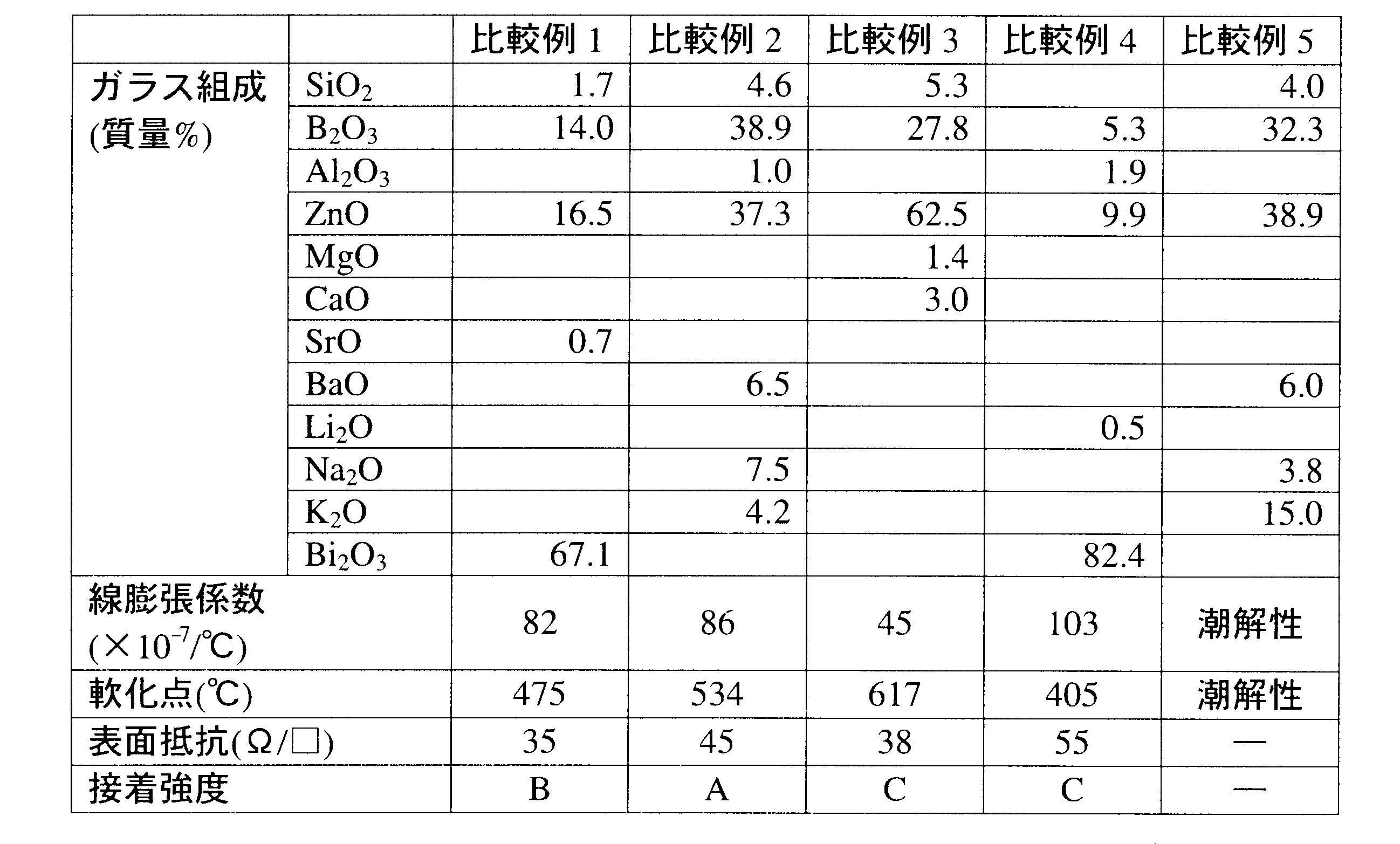
なお表1及び2の接着強度の欄において、Aは接着強度が良好であったことを示し、Bは接着強度がどちらかというと良好であったことを示し、Cは接着強度が不十分であったことを示す。
表1における実施例1~6に示すように、本発明の組成範囲内においては、軟化点が450℃~600℃であり、好適な熱膨張係数(70~110)×10-7/℃を有しており、p型半導体シリコン基板1との密着性も良好であった。更には、太陽電池素子の変換効率に関係するp+層7の抵抗値も26Ω/□以下となり、半導体シリコン太陽電池用の導電性ペーストとして用いることが可能である。
他方、本発明の組成範囲を外れる表2における比較例1~5は、p型半導体シリコン基板1との良好な密着性が得られない、p+層7の抵抗値が高い、または溶解後にガラスが潮解性を示すなど、半導体シリコン太陽電池用の導電性ペーストとしては適用し得ないものであった。
1 p型半導体シリコン基板
2 n型半導体シリコン層
3 反射防止膜
4 表面電極
5 アルミニウム電極層
6 BSF層
7 P+層
2 n型半導体シリコン層
3 反射防止膜
4 表面電極
5 アルミニウム電極層
6 BSF層
7 P+層
Claims (6)
- 半導体シリコン基板を用いる太陽電池用の導電性ペーストであって、該導電性ペーストはガラスフリットを含み、該ガラスフリットの組成は、実質的に鉛成分を含まず、質量%で
SiO2を1~20、
B2O3を5~30、
Al2O3を0~10、
ZnOを5~35、
RO(MgO、CaO、SrO、及びBaOからなる群から選ばれる少なくとも1種の合計)を5~30、
R2O(Li2O、Na2O、及びK2Oからなる群から選ばれる少なくとも1種の合計)を0.1~6、
Bi2O3を10~60、
を含むことを特徴とする導電性ペースト。 - 前記ガラスフリットは、30℃~300℃における熱膨張係数が(70~110)×10-7/℃、軟化点が450℃以上600℃以下であることを特徴とする請求項1に記載の導電性ペースト。
- 前記導電性ペーストはアルミニウム粉末を有することを特徴とする請求項1又は請求項2に記載の導電性ペースト。
- 前記ガラスフリットの組成において、R2Oとして少なくともK2Oを含むことを特徴とする請求項1乃至請求項3のいずれか1項に記載の導電性ペースト。
- 前記ガラスフリットの組成において、ROとして少なくともBaOを含むことを特徴とする請求項1乃至請求項4のいずれか1項に記載の導電性ペースト。
- 請求項1乃至請求項5のいずれか1項に記載の導電性ペーストを焼成させたアルミニウム電極層を有することを特徴とする太陽電池素子。
Priority Applications (2)
| Application Number | Priority Date | Filing Date | Title |
|---|---|---|---|
| CN201280005074.3A CN103314414B (zh) | 2011-02-10 | 2012-01-31 | 导电性糊剂及使用了该导电性糊剂的太阳能电池元件 |
| KR1020137020740A KR101455019B1 (ko) | 2011-02-10 | 2012-01-31 | 도전성 페이스트 및 그 도전성 페이스트를 사용한 태양전지 소자 |
Applications Claiming Priority (4)
| Application Number | Priority Date | Filing Date | Title |
|---|---|---|---|
| JP2011026781 | 2011-02-10 | ||
| JP2011-026781 | 2011-02-10 | ||
| JP2011270958A JP5888493B2 (ja) | 2011-02-10 | 2011-12-12 | 導電性ペースト及び該導電性ペーストを用いた太陽電池素子 |
| JP2011-270958 | 2011-12-12 |
Publications (1)
| Publication Number | Publication Date |
|---|---|
| WO2012108290A1 true WO2012108290A1 (ja) | 2012-08-16 |
Family
ID=46638506
Family Applications (1)
| Application Number | Title | Priority Date | Filing Date |
|---|---|---|---|
| PCT/JP2012/052055 Ceased WO2012108290A1 (ja) | 2011-02-10 | 2012-01-31 | 導電性ペースト及び該導電性ペーストを用いた太陽電池素子 |
Country Status (5)
| Country | Link |
|---|---|
| JP (1) | JP5888493B2 (ja) |
| KR (1) | KR101455019B1 (ja) |
| CN (1) | CN103314414B (ja) |
| TW (1) | TWI497739B (ja) |
| WO (1) | WO2012108290A1 (ja) |
Cited By (3)
| Publication number | Priority date | Publication date | Assignee | Title |
|---|---|---|---|---|
| CN103440900A (zh) * | 2013-09-10 | 2013-12-11 | 乐凯胶片股份有限公司 | 一种晶体硅太阳能电池用无铅正银浆料 |
| CN103440899A (zh) * | 2013-08-15 | 2013-12-11 | 广东风华高新科技股份有限公司 | 银电极浆料 |
| CN106396417A (zh) * | 2016-08-31 | 2017-02-15 | 安徽斯迈尔电子科技有限公司 | 一种大功率电阻中玻璃相的制备方法 |
Families Citing this family (10)
| Publication number | Priority date | Publication date | Assignee | Title |
|---|---|---|---|---|
| JP6155965B2 (ja) * | 2013-08-23 | 2017-07-05 | 旭硝子株式会社 | 電極形成用ガラス粉末および電極形成用導電ペースト |
| CN103617824B (zh) * | 2013-12-06 | 2016-10-05 | 苏州柏特瑞新材料有限公司 | 一种高附着力太阳能电池正面银浆及其制备方法 |
| JP2015115400A (ja) * | 2013-12-10 | 2015-06-22 | 東洋アルミニウム株式会社 | 導電性アルミニウムペースト |
| KR20170108577A (ko) * | 2016-03-18 | 2017-09-27 | 대주전자재료 주식회사 | 태양전지용 무연 도전 페이스트 |
| JP6688500B2 (ja) * | 2016-06-29 | 2020-04-28 | ナミックス株式会社 | 導電性ペースト及び太陽電池 |
| JP6714275B2 (ja) * | 2016-08-23 | 2020-06-24 | ナミックス株式会社 | 導電性ペースト及び太陽電池 |
| CN106571172A (zh) * | 2016-09-27 | 2017-04-19 | 东莞珂洛赫慕电子材料科技有限公司 | 一种铝合金基板厚膜电路中温烧结介质浆料及其制备方法 |
| CN109994247A (zh) * | 2017-12-29 | 2019-07-09 | 白金光学科技(苏州)有限公司 | 一种导电浆料 |
| JP7088811B2 (ja) * | 2018-11-09 | 2022-06-21 | Agc株式会社 | ガラス、ガラス粉末、導電ペーストおよび太陽電池 |
| JP7444552B2 (ja) * | 2019-06-04 | 2024-03-06 | Agc株式会社 | ガラス組成物、ガラス組成物の製造方法、導電ペースト、及び太陽電池 |
Citations (10)
| Publication number | Priority date | Publication date | Assignee | Title |
|---|---|---|---|---|
| JP2009120462A (ja) * | 2007-11-19 | 2009-06-04 | Asahi Glass Co Ltd | 色素増感型太陽電池製造用無鉛ガラスおよびガラスセラミックス組成物 |
| WO2010005629A1 (en) * | 2008-07-10 | 2010-01-14 | Ferro Corporation | Zinc containing glasses and enamels |
| WO2010011430A1 (en) * | 2008-06-26 | 2010-01-28 | E. I. Du Pont De Nemours And Company | Glass compositions used in conductors for photovoltaic cells |
| JP2010173904A (ja) * | 2009-01-30 | 2010-08-12 | Asahi Glass Co Ltd | ガラス組成物およびそれを用いた導電性ペースト |
| JP2010192480A (ja) * | 2009-02-16 | 2010-09-02 | Nippon Electric Glass Co Ltd | 電極形成用ガラス組成物および電極形成材料 |
| JP2010251138A (ja) * | 2009-04-16 | 2010-11-04 | Nippon Electric Glass Co Ltd | 電極形成用ガラス組成物および電極形成材料 |
| JP2010248034A (ja) * | 2009-04-16 | 2010-11-04 | Nippon Electric Glass Co Ltd | 電極形成用ガラス組成物および電極形成材料 |
| JP2010280554A (ja) * | 2009-06-08 | 2010-12-16 | Nippon Electric Glass Co Ltd | 色素増感型太陽電池用ガラスおよび色素増感型太陽電池用材料 |
| JP2011136890A (ja) * | 2009-12-29 | 2011-07-14 | Central Glass Co Ltd | 絶縁被覆用無鉛低融点ガラスペースト |
| JP2011207629A (ja) * | 2010-03-28 | 2011-10-20 | Central Glass Co Ltd | 低融点ガラス組成物及びそれを用いた導電性ペースト材料 |
Family Cites Families (3)
| Publication number | Priority date | Publication date | Assignee | Title |
|---|---|---|---|---|
| JP2001139345A (ja) * | 1999-11-10 | 2001-05-22 | Asahi Glass Co Ltd | 無鉛低融点ガラスおよびガラスフリット |
| US7176152B2 (en) * | 2004-06-09 | 2007-02-13 | Ferro Corporation | Lead-free and cadmium-free conductive copper thick film pastes |
| CN101840744B (zh) * | 2010-02-10 | 2012-04-25 | 武汉伊莱瑞尔高新技术有限公司 | 环保型无铅铝浆及其制备方法 |
-
2011
- 2011-12-12 JP JP2011270958A patent/JP5888493B2/ja not_active Expired - Fee Related
-
2012
- 2012-01-31 WO PCT/JP2012/052055 patent/WO2012108290A1/ja not_active Ceased
- 2012-01-31 KR KR1020137020740A patent/KR101455019B1/ko not_active Expired - Fee Related
- 2012-01-31 CN CN201280005074.3A patent/CN103314414B/zh not_active Expired - Fee Related
- 2012-02-10 TW TW101104460A patent/TWI497739B/zh not_active IP Right Cessation
Patent Citations (11)
| Publication number | Priority date | Publication date | Assignee | Title |
|---|---|---|---|---|
| JP2009120462A (ja) * | 2007-11-19 | 2009-06-04 | Asahi Glass Co Ltd | 色素増感型太陽電池製造用無鉛ガラスおよびガラスセラミックス組成物 |
| WO2010011430A1 (en) * | 2008-06-26 | 2010-01-28 | E. I. Du Pont De Nemours And Company | Glass compositions used in conductors for photovoltaic cells |
| WO2010011429A1 (en) * | 2008-06-26 | 2010-01-28 | E. I. Du Pont De Nemours And Company | Glass compositions used in conductors for photovoltaic cells |
| WO2010005629A1 (en) * | 2008-07-10 | 2010-01-14 | Ferro Corporation | Zinc containing glasses and enamels |
| JP2010173904A (ja) * | 2009-01-30 | 2010-08-12 | Asahi Glass Co Ltd | ガラス組成物およびそれを用いた導電性ペースト |
| JP2010192480A (ja) * | 2009-02-16 | 2010-09-02 | Nippon Electric Glass Co Ltd | 電極形成用ガラス組成物および電極形成材料 |
| JP2010251138A (ja) * | 2009-04-16 | 2010-11-04 | Nippon Electric Glass Co Ltd | 電極形成用ガラス組成物および電極形成材料 |
| JP2010248034A (ja) * | 2009-04-16 | 2010-11-04 | Nippon Electric Glass Co Ltd | 電極形成用ガラス組成物および電極形成材料 |
| JP2010280554A (ja) * | 2009-06-08 | 2010-12-16 | Nippon Electric Glass Co Ltd | 色素増感型太陽電池用ガラスおよび色素増感型太陽電池用材料 |
| JP2011136890A (ja) * | 2009-12-29 | 2011-07-14 | Central Glass Co Ltd | 絶縁被覆用無鉛低融点ガラスペースト |
| JP2011207629A (ja) * | 2010-03-28 | 2011-10-20 | Central Glass Co Ltd | 低融点ガラス組成物及びそれを用いた導電性ペースト材料 |
Cited By (3)
| Publication number | Priority date | Publication date | Assignee | Title |
|---|---|---|---|---|
| CN103440899A (zh) * | 2013-08-15 | 2013-12-11 | 广东风华高新科技股份有限公司 | 银电极浆料 |
| CN103440900A (zh) * | 2013-09-10 | 2013-12-11 | 乐凯胶片股份有限公司 | 一种晶体硅太阳能电池用无铅正银浆料 |
| CN106396417A (zh) * | 2016-08-31 | 2017-02-15 | 安徽斯迈尔电子科技有限公司 | 一种大功率电阻中玻璃相的制备方法 |
Also Published As
| Publication number | Publication date |
|---|---|
| KR20130121933A (ko) | 2013-11-06 |
| JP5888493B2 (ja) | 2016-03-22 |
| CN103314414A (zh) | 2013-09-18 |
| TW201242060A (en) | 2012-10-16 |
| JP2012180261A (ja) | 2012-09-20 |
| CN103314414B (zh) | 2015-09-16 |
| KR101455019B1 (ko) | 2014-10-28 |
| TWI497739B (zh) | 2015-08-21 |
Similar Documents
| Publication | Publication Date | Title |
|---|---|---|
| JP5888493B2 (ja) | 導電性ペースト及び該導電性ペーストを用いた太陽電池素子 | |
| JP5609319B2 (ja) | 低融点ガラス組成物及びそれを用いた導電性ペースト材料 | |
| JP5272373B2 (ja) | 多結晶Si太陽電池 | |
| CN102026927A (zh) | 在用于光伏电池的导体中使用的玻璃组合物 | |
| JP5796270B2 (ja) | 電極形成材料 | |
| JP5569094B2 (ja) | 低融点ガラス組成物及びそれを用いた導電性ペースト材料 | |
| JP5910509B2 (ja) | 導電性ペースト及び該導電性ペーストを用いた太陽電池素子 | |
| WO2013103087A1 (ja) | 電極形成用ガラス及びこれを用いた電極形成材料 | |
| JP5943295B2 (ja) | 電極形成用ガラス及びこれを用いた電極形成材料 | |
| JP5796281B2 (ja) | 電極形成材料 | |
| KR20140074415A (ko) | 태양전지 후면 전극의 제조 방법 및 이를 이용한 태양전지 소자 | |
| JP6112384B2 (ja) | 電極形成用ガラス及びこれを用いた電極形成材料 | |
| JP2013189372A (ja) | 導電性ペースト材料 | |
| JP2014105153A (ja) | ビスマス系ガラス組成物及びこれを用いた電極形成材料 | |
| JP2013212949A (ja) | 電極形成用ガラス及びこれを用いた電極形成材料 | |
| KR20130043805A (ko) | 알루미늄 페이스트 조성물 및 이를 이용한 태양전지 소자 | |
| KR20140052480A (ko) | 알루미늄 페이스트 조성물 및 이를 이용한 태양전지 소자 | |
| KR20130042366A (ko) | 알루미늄 페이스트 조성물 및 이를 이용한 태양전지 소자 |
Legal Events
| Date | Code | Title | Description |
|---|---|---|---|
| 121 | Ep: the epo has been informed by wipo that ep was designated in this application |
Ref document number: 12744300 Country of ref document: EP Kind code of ref document: A1 |
|
| ENP | Entry into the national phase |
Ref document number: 20137020740 Country of ref document: KR Kind code of ref document: A |
|
| NENP | Non-entry into the national phase |
Ref country code: DE |
|
| 122 | Ep: pct application non-entry in european phase |
Ref document number: 12744300 Country of ref document: EP Kind code of ref document: A1 |