WO2012108150A1 - マグネトロンスパッタリング装置、マグネトロンスパッタリング装置の制御方法、及び成膜方法 - Google Patents
マグネトロンスパッタリング装置、マグネトロンスパッタリング装置の制御方法、及び成膜方法 Download PDFInfo
- Publication number
- WO2012108150A1 WO2012108150A1 PCT/JP2012/000710 JP2012000710W WO2012108150A1 WO 2012108150 A1 WO2012108150 A1 WO 2012108150A1 JP 2012000710 W JP2012000710 W JP 2012000710W WO 2012108150 A1 WO2012108150 A1 WO 2012108150A1
- Authority
- WO
- WIPO (PCT)
- Prior art keywords
- target
- magnetron sputtering
- sputtering apparatus
- phase difference
- adjacent
- Prior art date
- Legal status (The legal status is an assumption and is not a legal conclusion. Google has not performed a legal analysis and makes no representation as to the accuracy of the status listed.)
- Ceased
Links
Images




Classifications
-
- C—CHEMISTRY; METALLURGY
- C23—COATING METALLIC MATERIAL; COATING MATERIAL WITH METALLIC MATERIAL; CHEMICAL SURFACE TREATMENT; DIFFUSION TREATMENT OF METALLIC MATERIAL; COATING BY VACUUM EVAPORATION, BY SPUTTERING, BY ION IMPLANTATION OR BY CHEMICAL VAPOUR DEPOSITION, IN GENERAL; INHIBITING CORROSION OF METALLIC MATERIAL OR INCRUSTATION IN GENERAL
- C23C—COATING METALLIC MATERIAL; COATING MATERIAL WITH METALLIC MATERIAL; SURFACE TREATMENT OF METALLIC MATERIAL BY DIFFUSION INTO THE SURFACE, BY CHEMICAL CONVERSION OR SUBSTITUTION; COATING BY VACUUM EVAPORATION, BY SPUTTERING, BY ION IMPLANTATION OR BY CHEMICAL VAPOUR DEPOSITION, IN GENERAL
- C23C14/00—Coating by vacuum evaporation, by sputtering or by ion implantation of the coating forming material
- C23C14/22—Coating by vacuum evaporation, by sputtering or by ion implantation of the coating forming material characterised by the process of coating
- C23C14/34—Sputtering
- C23C14/35—Sputtering by application of a magnetic field, e.g. magnetron sputtering
-
- C—CHEMISTRY; METALLURGY
- C23—COATING METALLIC MATERIAL; COATING MATERIAL WITH METALLIC MATERIAL; CHEMICAL SURFACE TREATMENT; DIFFUSION TREATMENT OF METALLIC MATERIAL; COATING BY VACUUM EVAPORATION, BY SPUTTERING, BY ION IMPLANTATION OR BY CHEMICAL VAPOUR DEPOSITION, IN GENERAL; INHIBITING CORROSION OF METALLIC MATERIAL OR INCRUSTATION IN GENERAL
- C23C—COATING METALLIC MATERIAL; COATING MATERIAL WITH METALLIC MATERIAL; SURFACE TREATMENT OF METALLIC MATERIAL BY DIFFUSION INTO THE SURFACE, BY CHEMICAL CONVERSION OR SUBSTITUTION; COATING BY VACUUM EVAPORATION, BY SPUTTERING, BY ION IMPLANTATION OR BY CHEMICAL VAPOUR DEPOSITION, IN GENERAL
- C23C14/00—Coating by vacuum evaporation, by sputtering or by ion implantation of the coating forming material
- C23C14/22—Coating by vacuum evaporation, by sputtering or by ion implantation of the coating forming material characterised by the process of coating
- C23C14/34—Sputtering
- C23C14/35—Sputtering by application of a magnetic field, e.g. magnetron sputtering
- C23C14/352—Sputtering by application of a magnetic field, e.g. magnetron sputtering using more than one target
-
- C—CHEMISTRY; METALLURGY
- C23—COATING METALLIC MATERIAL; COATING MATERIAL WITH METALLIC MATERIAL; CHEMICAL SURFACE TREATMENT; DIFFUSION TREATMENT OF METALLIC MATERIAL; COATING BY VACUUM EVAPORATION, BY SPUTTERING, BY ION IMPLANTATION OR BY CHEMICAL VAPOUR DEPOSITION, IN GENERAL; INHIBITING CORROSION OF METALLIC MATERIAL OR INCRUSTATION IN GENERAL
- C23C—COATING METALLIC MATERIAL; COATING MATERIAL WITH METALLIC MATERIAL; SURFACE TREATMENT OF METALLIC MATERIAL BY DIFFUSION INTO THE SURFACE, BY CHEMICAL CONVERSION OR SUBSTITUTION; COATING BY VACUUM EVAPORATION, BY SPUTTERING, BY ION IMPLANTATION OR BY CHEMICAL VAPOUR DEPOSITION, IN GENERAL
- C23C14/00—Coating by vacuum evaporation, by sputtering or by ion implantation of the coating forming material
- C23C14/06—Coating by vacuum evaporation, by sputtering or by ion implantation of the coating forming material characterised by the coating material
- C23C14/08—Oxides
-
- C—CHEMISTRY; METALLURGY
- C23—COATING METALLIC MATERIAL; COATING MATERIAL WITH METALLIC MATERIAL; CHEMICAL SURFACE TREATMENT; DIFFUSION TREATMENT OF METALLIC MATERIAL; COATING BY VACUUM EVAPORATION, BY SPUTTERING, BY ION IMPLANTATION OR BY CHEMICAL VAPOUR DEPOSITION, IN GENERAL; INHIBITING CORROSION OF METALLIC MATERIAL OR INCRUSTATION IN GENERAL
- C23C—COATING METALLIC MATERIAL; COATING MATERIAL WITH METALLIC MATERIAL; SURFACE TREATMENT OF METALLIC MATERIAL BY DIFFUSION INTO THE SURFACE, BY CHEMICAL CONVERSION OR SUBSTITUTION; COATING BY VACUUM EVAPORATION, BY SPUTTERING, BY ION IMPLANTATION OR BY CHEMICAL VAPOUR DEPOSITION, IN GENERAL
- C23C14/00—Coating by vacuum evaporation, by sputtering or by ion implantation of the coating forming material
- C23C14/22—Coating by vacuum evaporation, by sputtering or by ion implantation of the coating forming material characterised by the process of coating
- C23C14/54—Controlling or regulating the coating process
-
- H—ELECTRICITY
- H01—ELECTRIC ELEMENTS
- H01J—ELECTRIC DISCHARGE TUBES OR DISCHARGE LAMPS
- H01J37/00—Discharge tubes with provision for introducing objects or material to be exposed to the discharge, e.g. for the purpose of examination or processing thereof
- H01J37/32—Gas-filled discharge tubes
- H01J37/34—Gas-filled discharge tubes operating with cathodic sputtering
- H01J37/3402—Gas-filled discharge tubes operating with cathodic sputtering using supplementary magnetic fields
- H01J37/3405—Magnetron sputtering
- H01J37/3408—Planar magnetron sputtering
-
- H—ELECTRICITY
- H01—ELECTRIC ELEMENTS
- H01J—ELECTRIC DISCHARGE TUBES OR DISCHARGE LAMPS
- H01J37/00—Discharge tubes with provision for introducing objects or material to be exposed to the discharge, e.g. for the purpose of examination or processing thereof
- H01J37/32—Gas-filled discharge tubes
- H01J37/34—Gas-filled discharge tubes operating with cathodic sputtering
- H01J37/3411—Constructional aspects of the reactor
- H01J37/3444—Associated circuits
-
- H—ELECTRICITY
- H01—ELECTRIC ELEMENTS
- H01J—ELECTRIC DISCHARGE TUBES OR DISCHARGE LAMPS
- H01J37/00—Discharge tubes with provision for introducing objects or material to be exposed to the discharge, e.g. for the purpose of examination or processing thereof
- H01J37/32—Gas-filled discharge tubes
- H01J37/34—Gas-filled discharge tubes operating with cathodic sputtering
- H01J37/3464—Operating strategies
Definitions
- the present invention relates to a magnetron sputtering apparatus, a control method of a magnetron sputtering apparatus, and a film forming method.
- a sputtering method is generally known as a method for forming a thin film on the surface of a substrate.
- the sputtering method is widely known as a dry process technique indispensable for a film forming technique.
- a rare gas such as Ar gas is introduced into a vacuum vessel, direct current (DC) power or high frequency (RF, AC) power is supplied to a cathode including a target to generate glow discharge, and film formation is performed. How to do it.
- the sputtering method includes a magnetron sputtering method in which a magnet is disposed on the back surface of the target in an electrically grounded chamber to increase the plasma density in the vicinity of the target surface so that film formation can be performed at high speed.
- a sputtering method is used in a process of forming a predetermined thin film on a processing substrate having a large area such as a glass substrate constituting a liquid crystal display panel or the like.
- Patent Document 1 discloses that the substrate 111 to be processed is parallel to the substrate 111.
- a magnetron sputtering apparatus 100 having a plurality of first targets 101 and a plurality of second targets 102 arranged is disclosed.
- the plurality of first targets 101 are arranged in parallel to each other, and their one ends are connected to each other, thereby forming a comb-like shape as a whole.
- the plurality of second targets 102 are also arranged in parallel to each other, and one end thereof is connected to each other, thereby forming a comb-like shape as a whole.
- the first target 101 and the second target are alternately arranged so that the comb teeth of the first target 101 and the second target 102 mesh with each other.
- One high frequency power source 103 is connected to the plurality of first targets 101.
- one high-frequency power source 104 is connected to the plurality of second targets 102.
- each of the first and second targets 101 and 102 is energized with a high-frequency current whose phase is shifted by 180 ° between the first target 101 and the second target 102.
- Glow discharge is generated while the anode electrode and the cathode electrode are alternately switched between the pair of first and second targets 101 and 102.
- a plasma atmosphere is formed in the chamber, and a thin film 111 is formed on the surface of the substrate 110 by sputtering.
- a sputtering apparatus disclosed in Patent Document 2 includes a plurality of targets arranged in a vacuum chamber, a direct current power source and a high frequency power source, an impedance matching circuit provided between the high frequency power source and the target, a direct current A switch unit provided between the power source and the target and a phase shifter connected to the high frequency power source are provided.
- a high-frequency current intermittently output from the high-frequency power source is supplied to each target via the impedance matching circuit, and a direct-current output intermittently from the DC power source is superimposed on the high-frequency current. It has become. As a result, the dielectric film is uniformly and efficiently formed on a large substrate.
- the present invention has been made in view of such various points, and an object of the present invention is to stabilize the plasma state while avoiding complication of the apparatus configuration.
- a magnetron sputtering apparatus includes a target unit on which a substrate to be processed is disposed so as to face each other, an AC power source that supplies power to the target unit, and the target unit. And a magnet unit that reciprocally moves, wherein a plurality of first targets and second targets are alternately arranged in the target unit, and the first target and the second target adjacent to each other.
- a plurality of sets are provided, and the first target and the second target are connected to the AC power source for each of the sets, and are connected to the first target and the second target in the set adjacent to each other.
- a control unit for controlling the phase difference between the voltages output from the AC power supply is provided.
- the method for controlling a magnetron sputtering apparatus includes a target unit on which a substrate to be processed is disposed facing, an AC power source that supplies power to the target unit, and a reciprocating movement along the target unit. And a magnetron sputtering apparatus in which a plurality of first targets and second targets are alternately arranged and a plurality of pairs of the first target and the second target adjacent to each other are provided in the target portion.
- a method of controlling wherein the AC power supply is connected to the first target and the second target for each set, and the first target and the second target are connected to each other in the set adjacent to each other. The phase difference of each voltage output from the AC power supply is controlled.
- a film forming method includes a target unit on which a substrate to be processed is disposed to face, an AC power source that supplies power to the target unit, and a magnet unit that reciprocates along the target unit.
- a plurality of first targets and second targets are alternately arranged on the target unit, and the substrate is formed by a magnetron sputtering apparatus provided with a plurality of sets of the first target and the second target adjacent to each other.
- the AC power supply is connected to the first target and the second target for each set, and the first target and the second target are connected to each other in the set adjacent to each other.
- a thin film is formed on the surface of the substrate by controlling the phase difference between the voltages output from the connected AC power supplies.
- an AC power supply is connected for each set to the first target and the second target, and is output from the AC power supply connected to the first target and the second target in a set adjacent to each other. Since the phase difference of each voltage is controlled, it is possible to stabilize the plasma state by suppressing the voltage applied to the first target and the second target from interfering with each other in each adjacent pair. become. In addition, since a DC power supply, a switch unit for controlling the DC power supply, and the like are not required, complication of the apparatus configuration can be avoided.
- FIG. 1 is a cross-sectional view illustrating a schematic configuration of a magnetron sputtering apparatus according to the first embodiment.
- FIG. 2 is a plan view showing a target portion in the first embodiment.
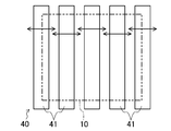
- FIG. 3 is a plan view showing the positional relationship between the magnet unit and the substrate in the first embodiment.
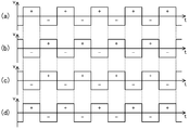
- FIG. 4A is a graph showing a voltage wave applied to the first target.
- FIG. 4B is a graph showing a voltage wave applied to the second target.
- FIG. 4C is a graph showing a voltage wave applied to the first target.
- FIG. 4D is a graph showing a voltage wave applied to the second target.
- FIG. 5A is a graph showing a voltage wave applied to the first target.
- FIG. 5B is a graph showing a voltage wave applied to the second target.
- FIG. 5C is a graph showing a voltage wave applied to the first target.
- FIG. 5D is a graph showing a voltage wave applied to the second target.
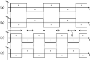
- FIG. 6A is a graph showing a voltage wave applied to the first target.
- FIG. 6B is a graph showing a voltage wave applied to the second target.
- FIG. 6C is a graph showing a voltage wave applied to the first target.
- FIG. 6D is a graph showing a voltage wave applied to the second target.
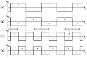
- FIG. 7A is a graph showing a voltage wave applied to the first target.
- FIG. 7B is a graph showing a voltage wave applied to the second target.
- FIG. 7C is a graph showing a voltage wave applied to the first target.
- FIG. 7D is a graph showing a voltage wave applied to the second target.
- FIG. 8 is an enlarged cross-sectional view showing an example of a main part of a conventional magnetron sputtering apparatus.
- FIG. 9 is an enlarged plan
- Embodiment 1 of the Invention 1 to 4 show Embodiment 1 of the present invention.
- FIG. 1 is a cross-sectional view showing a schematic configuration of a magnetron sputtering apparatus 1 according to the first embodiment.
- FIG. 2 is a plan view showing the target unit 20 in the first embodiment.
- FIG. 3 is a plan view showing the positional relationship between the magnet unit 40 and the substrate 10 in the first embodiment.
- FIG. 4 is a graph showing a voltage waveform subjected to power supply control in the first embodiment.
- the magnetron sputtering apparatus 1 includes a substrate holding unit 11 that holds a substrate 10 to be processed and a target unit in which the substrate 10 held by the substrate holding unit 11 is opposed to the target unit. 20, an AC power supply 30 for supplying power to the target unit 20, a magnet unit 40 disposed on the back side of the target unit 20, which is opposite to the substrate 10 of the target unit 20, and the substrate holding unit 11. And a chamber 50 for accommodating the target unit 20.
- the chamber 50 is a vacuum chamber, and its side wall 51 is electrically grounded.
- a vacuum pump (not shown) is connected to the chamber 50, and the inside of the chamber 50 is depressurized by the vacuum pump.
- the chamber 50 is provided with a gas supply unit (not shown).
- the gas supply unit is configured to introduce Ar gas and, if necessary, O 2 gas into the vacuum chamber 50.
- the substrate 10 is a substrate such as a glass substrate constituting a liquid crystal display panel (not shown), for example.
- the size of the substrate 10 is, for example, 730 mm in length and 920 mm in width.
- the substrate holding unit 11 has a heater (not shown) that holds the substrate 10 on its lower surface and heats the substrate 10 during film formation.
- a substrate mask 24 that covers the outer edge portion of the lower surface of the substrate 10 is provided.
- first targets 25 and a plurality of second targets 26 are alternately arranged on the target unit 20.
- the first target 25 and the second target 26 are each formed, for example, in the same rectangular plate shape, and are predetermined in the short side direction (the left-right direction in FIGS. 1 and 2 and the moving direction of the magnet unit 40 described later). Arranged at intervals. Therefore, the long side portion of the first target 25 is adjacent to the long side portion of the second target 26.
- the target unit 20 is provided with a plurality of sets 21 of the first target 25 and the second target 26 adjacent to each other.
- the target unit 20 in the present embodiment has two sets 21 of the first target 25 and the second target 26. That is, as shown in FIG. 1, the target unit 20 includes a set 21 of a first target 25a and a second target 26b, and a set 21 of a first target 25c and a second target 26d.
- the first and second targets 25 and 26 are made of, for example, a material including IGZO (In—Ga—ZnO 4 ; amorphous oxide semiconductor), ITO, Ti, Al, Mo, Cu, IZO, Al alloy, or Cu alloy. It is configured.
- the target unit 20 is supported by the target support unit 22.
- the target support portion 22 is formed of a conductive material such as Cu, for example.
- the target support portion 22 is installed on the insulating member 23.
- the AC power supply 30 is connected to the first and second targets 25 and 26 via the target support portion 22 for each group 21. As shown in FIG. 4, each AC power supply 30 applies AC drive voltages having the same frequency to the target unit 20 via the target support unit 22.
- the frequency of the drive voltage of the AC power supply 30 is 1 MHz or less, for example, about 19 kHz to 20 kHz.
- the magnet unit 40 is configured to reciprocate along the target unit 20 by a drive mechanism (not shown). As shown in FIG. 1, the magnet unit 40 has a plurality of magnets 41 arranged at predetermined intervals in the moving direction of the magnet unit 40 (left and right direction in FIG. 1).
- the magnets 41 swing in synchronization with each other.
- the swing speed is, for example, about 15 mm / s to 30 mm / s.
- the swing width of each magnet 41 is substantially the same as the width of the first and second targets 25 and 26 (that is, the width of the magnet unit 40 in the moving direction).
- the width of the magnet 41 is smaller than the width of the first and second targets 25 and 26.
- the width of the magnet 41 is, for example, about half of the width of the first and second targets 25 and 26.
- the said magnetron sputtering apparatus 1 has the control part 60 which controls the phase difference of the voltage output from the alternating current power supply 30.
- FIG. In the present embodiment, one control unit 60 is commonly connected to the plurality of AC power sources 30.
- the controller 60 controls the phase difference between the voltages output from the AC power supply 30 connected to the first target 25 and the second target 26 in the adjacent sets 21.
- the graph in FIG. 4A shows a voltage wave applied to the first target 25a.
- the graph of FIG. 4B shows a voltage wave applied to the second target 26b.
- the graph in FIG. 4C shows a voltage wave applied to the first target 25c.
- the graph of FIG.4 (d) shows the voltage wave applied to the 2nd target 26d.
- the horizontal axis represents time (t), while the vertical axis represents voltage (V).
- the controller 60 is included in different sets 21 and applied to the first target 25c and the second target 26b adjacent to each other so that the phases of the voltages are the same (that is, the phase difference ⁇ is 0). Control the phase difference ⁇ .
- the first target 25c included in the right set 21 in FIG. 1 is adjacent to the second target 26b included in the left set 21 in FIG.
- the frequency of the voltage applied to the 1st target 25c and the 2nd target 26b is the same.
- the phases of the voltages applied to the first target 25c and the second target 26b are the same.
- input power density of the AC power supply 30 is 1.0W / cm 2 ⁇ 4.0W / cm 2 approximately.
- a glow discharge is generated between the first target 25 and the second target 26 b and a glow discharge is generated between the first target 25 c and the second target 26 d.
- a plasma atmosphere is formed in the chamber 50, and a thin film is formed on the surface of the substrate 10 by sputtering.
- the substrate 10 that is a glass substrate is carried into the chamber 50 and is held by the substrate holding unit 11.
- the inside of the chamber 50 is depressurized by a vacuum pump (not shown), and the substrate 10 is heated by a heater (not shown) of the substrate holder 11.
- the targets 25 and 26 are made of a material containing, for example, IGZO (In—Ga—ZnO 4 ; amorphous oxide semiconductor), ITO, Ti, Al, Mo, Cu, IZO, Al alloy, or Cu alloy.
- a gas supply unit (not shown).
- a predetermined alternating voltage is applied from the alternating current power source 30 to supply power to the target unit 20, and film formation is started by swinging the magnet unit 40.
- the swing speed of the magnet unit 40 is, for example, about 15 mm / s to 30 mm / s.
- the voltage output from the AC power supply 30 is controlled by the control unit 60. That is, the control unit 60 controls the phase difference of the voltage applied from the AC power supply 30 to the first target 25 and the second target 26 of each set 21 for each set 21 of the first target 25 and the second target 26. To do.
- the phases of the voltages applied to the first target 25 and the second target 26 included in each set 21 are shifted from each other by 180 °. Therefore, as shown in the graph of FIG. 4, the plus and minus of the voltage are switched at the same timing for each group 21.
- control unit 60 includes the voltage applied to the first target 25c and the second target 26b that are included in different sets 21 and are adjacent to each other, so that the phase difference ⁇ is 0. Control the voltage.
- Input power density of the AC power supply 30 is 1.0W / cm 2 ⁇ 4.0W / cm 2 approximately.
- one glow discharge occurs between the first target 25a and the second target 26b, and a glow discharge occurs between the first target 25c and the second target 26d.
- a plasma atmosphere is formed in the chamber 50, and Ar positively ionized by the plasma is attracted to each first target 25 or second target 26.
- Ar ions collide with the targets 25 and 26, and the constituent particles of the targets 25 and 26 are blown off and adhere to the substrate 10. In this way, film formation is performed on the surface of the substrate 10.
- the phases of the voltages applied to the first target 25c and the second target 26b that are included in different sets 21 and are adjacent to each other are the same (that is, the phase difference ⁇ is 0).
- the phase difference ⁇ is controlled by the controller 60, it is possible to suppress the voltages applied to the first target 25c and the second target 26b from interfering with each other.
- the configuration of the DC power source and the switch unit for controlling the DC power source is not required, so that the device configuration can be prevented from becoming complicated.
- FIG. 5 shows Embodiment 2 of the present invention.
- FIG. 5 is a graph showing voltage waveforms subjected to power supply control in the second embodiment.
- FIG. 5A is a graph showing a voltage wave applied to the first target 25a.
- FIG. 5B is a graph showing a voltage wave applied to the second target 26b.
- FIG. 5C is a graph showing a voltage wave applied to the first target 25c.
- FIG. 5D is a graph showing a voltage wave applied to the second target 26d.
- the horizontal axis represents time (t), while the vertical axis represents voltage (V).
- the phase difference is controlled so that the phases of the voltages applied to the first target 25c and the second target 26b are the same as each other.
- the phase difference is shifted within a predetermined range.
- the substrate holding unit 11 that holds the substrate 10 to be processed and the substrate 10 held by the substrate holding unit 11 are opposed to each other as in the first embodiment.
- Target unit 20 AC power supply 30 for supplying power to the target unit 20, magnet unit 40 disposed on the back side of the target unit 20 opposite to the substrate 10 of the target unit 20, and the substrate A holding unit 11 and a chamber 50 that accommodates the target unit 20 are provided.
- the target part 20 in this Embodiment 2 has the group 21 of the 1st target 25a and the 2nd target 26b, and the group 21 of the 1st target 25c and the 2nd target 26d similarly to the said Embodiment 1.
- the first and second targets 25 and 26 are made of a material containing, for example, IGZO, ITO, Ti, Al, Mo, Cu, IZO, Al alloy, or Cu alloy.
- the said magnetron sputtering apparatus 1 has the control part 60 which controls the phase difference of the voltage output from the alternating current power supply 30.
- FIG. The control unit 60 of the present embodiment determines the level of the voltage applied from each AC power supply 30 to the first target 25 and the second target 26 of each set 21 for each set 21 of the first target 25 and the second target 26. Control the phase difference.
- the phases of the voltages applied to the first target 25 and the second target 26 included in each set 21 are shifted from each other by 180 °.
- control unit 60 includes a phase difference ⁇ of voltages applied to the first target 25c and the second target 26b that are included in mutually different sets 21 and adjacent to each other, and ⁇ 90 ° ⁇ ⁇ ⁇ .
- the phase difference is controlled so as to be within the range of 90 °.
- the control unit 60 shifts the phase of the voltage applied to the first target 25c by, for example, ⁇ 60 ° with respect to the phase of the voltage applied to the second target 26b.
- the phase difference ⁇ between the first target 25c and the second target 26b is, for example, ⁇ 60 °. Even in this case, the plasma state can be preferably stabilized.
- the substrate 10 which is a glass substrate, is carried into the chamber 50 and is held by the substrate holding unit 11.
- the inside of the chamber 50 is depressurized by a vacuum pump (not shown), and the substrate 10 is heated by a heater (not shown) of the substrate holder 11.
- the voltage output from the AC power supply 30 is controlled by the control unit 60. That is, the control unit 60 controls the phase difference of the voltage applied from the AC power supply 30 to the first target 25 and the second target 26 of each set 21 for each set 21 of the first target 25 and the second target 26. To do. The phases of the voltages applied to the first target 25 and the second target 26 included in each set 21 are shifted from each other by 180 °.
- control unit 60 includes voltages that are included in mutually different sets 21 and applied to the first target 25c and the second target 26b adjacent to each other, have the same frequency, and have a phase difference ⁇ of ⁇ 90 ° ⁇ ⁇ ⁇ .
- the voltage is controlled so as to be within a range of 90 °.
- Input power density of the AC power supply 30 is 1.0W / cm 2 ⁇ 4.0W / cm 2 approximately.
- one glow discharge occurs between the first target 25a and the second target 26b, and a glow discharge occurs between the first target 25c and the second target 26d.
- a plasma atmosphere is formed in the chamber 50, and Ar positively ionized by the plasma is attracted to each first target 25 or second target 26.
- Ar ions collide with the targets 25 and 26, and the constituent particles of the targets 25 and 26 are blown off and adhere to the substrate 10. In this way, film formation is performed on the surface of the substrate 10.
- the phase difference ⁇ of the voltages applied to the first target 25c and the second target 26b included in different sets 21 and adjacent to each other is in the range of ⁇ 90 ° ⁇ ⁇ ⁇ 90 °. Since the phase difference ⁇ is controlled by the control unit 60 so that the voltage applied to the first target 25c and the second target 26b can be prevented from interfering with each other. As a result, it is possible to reliably generate a glow discharge between the first target 25 and the second target 26 of each set 21 that is the original combination, and to stabilize the plasma state generated in the chamber 50.
- the configuration of the DC power source and the switch unit for controlling the DC power source is not required, so that the device configuration can be prevented from becoming complicated.
- the phase difference ⁇ is smaller than ⁇ 90 ° and larger than 90 °
- glow discharge occurs between the first target 25c and the second target 26b which are not the original combination.
- the amount of ions contained in the plasma generated between the first target 25a and the second target 26b included in one set 21 is such that the second target 26b of the set 21 and the first target of the other set 21 are the first. This is less than the amount of ions contained in the plasma generated between the target 26c. For this reason, the voltages applied to the targets 25 and 26 of each group 21 greatly interfere with each other, and the plasma state becomes unstable.
- the phase difference ⁇ is in the range of ⁇ 90 ° ⁇ ⁇ ⁇ 90 °
- the amount of ions included in the plasma generated between the first target 25a and the second target 26b included in one set 21 is larger. Therefore, the voltage applied to each set of targets 25 and 26 does not significantly interfere with each other, and the plasma state is stabilized. Therefore, as described above, when the phase difference ⁇ is in the range of ⁇ 90 ° ⁇ ⁇ ⁇ 90 °, the plasma state can be preferably stabilized.
- FIG. 6 shows Embodiment 3 of the present invention.
- FIG. 6 is a graph showing voltage waveforms subjected to power supply control in the third embodiment.
- FIG. 6A is a graph showing a voltage wave applied to the first target 25a.
- FIG. 6B is a graph showing a voltage wave applied to the second target 26b.
- FIG. 6C is a graph showing a voltage wave applied to the first target 25c.
- FIG. 6D is a graph showing a voltage wave applied to the second target 26d.
- the horizontal axis represents time (t), while the vertical axis represents voltage (V).
- the frequency of the voltage applied to each of the targets 25 and 26 is the same between the groups 21.
- the frequency of the voltage applied between the groups 21 is the same. They are different from each other under predetermined conditions.
- the substrate holding unit 11 that holds the substrate 10 to be processed and the substrate 10 held by the substrate holding unit 11 face each other.
- the target unit 20 in the third embodiment includes a set 21 of the first target 25a and the second target 26b and a set 21 of the first target 25c and the second target 26d, as in the first and second embodiments.
- the first and second targets 25 and 26 are made of a material containing, for example, IGZO, ITO, Ti, Al, Mo, Cu, IZO, Al alloy, or Cu alloy.
- the said magnetron sputtering apparatus 1 has the control part 60 which controls the phase difference of the voltage output from the alternating current power supply 30.
- FIG. The control unit 60 according to the present embodiment provides a phase difference between voltages applied to the first target 25 and the second target 26 of each set 21 from the AC power supply 30 for each set 21 of the first target 25 and the second target 26. To control. The phases of the voltages applied to the first target 25 and the second target 26 included in each set 21 are shifted from each other by 180 °.
- the control unit 60 includes a phase difference ⁇ of voltages applied to the first target 25c and the second target 26b that are included in different sets 21 and are adjacent to each other so that the phase difference ⁇ is in a range of ⁇ 90 ° ⁇ ⁇ ⁇ 90 °.
- the phase difference is controlled.
- one of the AC power supplies 30 connected to the first target 25 and the second target 26 in the adjacent sets 21 is an integer of the frequency of the voltage output from the other AC power supply 30. It is configured to output a voltage having a frequency that is not doubled.
- the frequency of the voltage applied to the first target 25a and the second target 26b of one set 21 is set to 20 kHz, for example, while the first target 25c and the second target 21c of the other set 21 are set.
- the frequency of the voltage applied to the target 26d is, for example, 30 kHz. That is, the other frequency is set to 1.5 times one frequency.
- the substrate 10 which is a glass substrate, is carried into the chamber 50 and is held by the substrate holding unit 11.
- the inside of the chamber 50 is depressurized by a vacuum pump (not shown), and the substrate 10 is heated by a heater (not shown) of the substrate holder 11.
- the voltage output from the AC power supply 30 is controlled by the control unit 60. That is, the control unit 60 controls the phase difference of the voltage applied from the AC power supply 30 to the first target 25 and the second target 26 of each set 21 for each set 21 of the first target 25 and the second target 26. To do. The phases of the voltages applied to the first target 25 and the second target 26 included in each set 21 are shifted from each other by 180 °.
- control unit 60 includes voltages that are included in mutually different sets 21 and applied to the first target 25c and the second target 26b adjacent to each other, have the same frequency, and have a phase difference ⁇ of ⁇ 90 ° ⁇ ⁇ ⁇ . The voltage is controlled so as to be within a range of 90 °.
- Input power density of the AC power supply 30 is 1.0W / cm 2 ⁇ 4.0W / cm 2 approximately.
- one of the AC power supplies 30 connected to the first target 25 and the second target 26 in the adjacent sets 21 outputs a voltage having a frequency that is not an integral multiple of the frequency output from the other AC power supply 30.
- the frequency of the voltage applied to the first target 25 a and the second target 26 b of one set 21 is set to 20 kHz, for example, while the first target 25 c and the second target 21 of the other set 21 are set.
- the frequency of the voltage applied to the target 26d is set to 30 kHz which is 1.5 times the frequency.
- one glow discharge occurs between the first target 25a and the second target 26b, and a glow discharge occurs between the first target 25c and the second target 26d.
- a plasma atmosphere is formed in the chamber 50, and Ar positively ionized by the plasma is attracted to each first target 25 or second target 26.
- Ar ions collide with the targets 25 and 26, and the constituent particles of the targets 25 and 26 are blown off and adhere to the substrate 10. In this way, film formation is performed on the surface of the substrate 10.
- FIG. 7 is a graph showing a voltage waveform subjected to power control in the comparative example.
- FIG. 7A is a graph showing a voltage wave applied to the first target 25a.
- FIG. 7B is a graph showing a voltage wave applied to the second target 26b.
- FIG. 7C is a graph showing a voltage wave applied to the first target 25c.
- FIG. 7D is a graph showing a voltage wave applied to the second target 26d.
- the horizontal axis represents time (t), while the vertical axis represents voltage (V).
- the frequency of the voltage applied to the first target 25a and the second target 26b of one set 21 is set to 20 kHz, for example, while the voltage applied to the first target 25c and the second target 26d of the other set 21 is The frequency is doubled to 40 kHz.
- the periods A in which the polarities of the applied voltages are different from each other for the first target 25 c and the second target 26 b that are included in the different sets 21 and are adjacent to each other are relatively Appears periodically in a long time.
- the plasma generated in each of the first target 25a and the second target 26b, which is the original combination, and the first target 25c and the second target 26d is reduced, so that the sputtering amount is greatly reduced periodically.
- the film quality of the thin film formed on the substrate 10 deteriorates due to destabilization of plasma.
- the periods B in which the polarities of the applied voltages are different from each other are distributed relatively short for the first target 25c and the second target 26b. be able to. Therefore, in each of the first target 25a and the second target 26b, which is the original combination, and the first target 25c and the second target 26d, the period during which plasma is reduced is long and does not appear periodically. The plasma state can be stabilized and the film quality of the thin film sputtered on the substrate 10 can be improved.
- the configuration of the DC power source and the switch unit for controlling the DC power source is not required, so that the device configuration can be prevented from becoming complicated.
- the present invention is not limited to the first to third embodiments, and the present invention includes a configuration in which these first to third embodiments are appropriately combined.
- the present invention is useful for a magnetron sputtering apparatus, a control method for a magnetron sputtering apparatus, and a film forming method.
Landscapes
- Chemical & Material Sciences (AREA)
- Engineering & Computer Science (AREA)
- Chemical Kinetics & Catalysis (AREA)
- Materials Engineering (AREA)
- Mechanical Engineering (AREA)
- Metallurgy (AREA)
- Organic Chemistry (AREA)
- Physics & Mathematics (AREA)
- Plasma & Fusion (AREA)
- Analytical Chemistry (AREA)
- Physical Vapour Deposition (AREA)
Abstract
Description
図1~図4は、本発明の実施形態1を示している。
次に、上記マグネトロンスパッタリング装置1の制御方法及び成膜方法について説明する。
したがって、この実施形態1によると、互いに異なる組21に含まれると共に互いに隣り合う第1ターゲット25c及び第2ターゲット26bに印加される電圧の位相が互いに同じ(つまり、位相差θが0)となるように、当該位相差θを制御部60によって制御するようにしたので、上記第1ターゲット25c及び第2ターゲット26bに印加される電圧が互いに干渉するのを抑制することができる。その結果、本来の組合せである各組21の第1ターゲット25と第2ターゲット26との間で確実にグロー放電を生じさせて、チャンバ50内に発生させるプラズマ状態を安定化させることができる。しかも、例えば直流電源やその直流電源を制御するスイッチユニット等の構成が不要になるため、装置構成の複雑化を回避することができる。
図5は、本発明の実施形態2を示している。
次に、本実施形態2における上記マグネトロンスパッタリング装置1の制御方法及び成膜方法について説明する。
したがって、この実施形態2によると、互いに異なる組21に含まれると共に互いに隣り合う第1ターゲット25c及び第2ターゲット26bに印加される電圧の位相差θが-90°≦θ≦90°の範囲内となるように、当該位相差θを制御部60によって制御するようにしたので、上記第1ターゲット25c及び第2ターゲット26bに印加される電圧が互いに干渉するのを抑制することができる。その結果、本来の組合せである各組21の第1ターゲット25と第2ターゲット26との間で確実にグロー放電を生じさせて、チャンバ50内に発生させるプラズマ状態を安定化させることができる。しかも、例えば直流電源やその直流電源を制御するスイッチユニット等の構成が不要になるため、装置構成の複雑化を回避することができる。
図6は、本発明の実施形態3を示している。
次に、本実施形態3における上記マグネトロンスパッタリング装置1の制御方法及び成膜方法について説明する。
ここで、図7は、比較例における電源制御をした電圧波形を示すグラフである。図7(a)は、第1ターゲット25aに印加される電圧波を示すグラフである。図7(b)は、第2ターゲット26bに印加される電圧波を示すグラフである。図7(c)は、第1ターゲット25cに印加される電圧波を示すグラフである。また、図7(d)は、第2ターゲット26dに印加される電圧波を示すグラフである。また、横軸は時間(t)を示す一方、縦軸は電圧(V)を示す。
10 基板
11 基板保持部
20 ターゲット部
21 ターゲットの組
25,25a,25c 第1ターゲット
26,26b,26d 第2ターゲット
30 電源
40 マグネット部
41 マグネット
60 制御部
Claims (13)
- 処理対象の基板が対向配置されるターゲット部と、
上記ターゲット部に対して電力を供給する交流電源と、
上記ターゲット部に沿って往復移動するマグネット部とを備えたマグネトロンスパッタリング装置であって、
上記ターゲット部には、第1ターゲット及び第2ターゲットが交互に複数配置されると共に、互いに隣り合う上記第1ターゲット及び第2ターゲットの組が複数設けられ、
上記第1ターゲット及び第2ターゲットには、上記各組毎に上記交流電源が接続され、
互いに隣り合う上記組において上記第1ターゲット及び第2ターゲットに接続されている上記交流電源からそれぞれ出力される各電圧の位相差を制御する制御部を備えている
ことを特徴とするマグネトロンスパッタリング装置。 - 請求項1に記載されたマグネトロンスパッタリング装置において、
上記制御部は、互いに異なる上記組に含まれると共に互いに隣り合う上記第1ターゲット及び第2ターゲットに印加される電圧の位相差θが-90°≦θ≦90°の範囲内となるように、上記位相差を制御する
ことを特徴とするマグネトロンスパッタリング装置。 - 請求項2に記載されたマグネトロンスパッタリング装置において、
互いに隣り合う上記組において上記第1ターゲット及び第2ターゲットに接続されている上記交流電源の一方は、他方の上記交流電源から出力される電圧の周波数の整数倍でない周波数の電圧を出力するように構成されている
ことを特徴とするマグネトロンスパッタリング装置。 - 請求項2に記載されたマグネトロンスパッタリング装置において、
互いに隣り合う上記組において上記第1ターゲット及び第2ターゲットに接続されている上記交流電源の周波数は、互いに同じであり、
上記制御部は、互いに異なる上記組に含まれると共に互いに隣り合う上記第1ターゲット及び第2ターゲットに印加される電圧の位相が互いに同じとなるように、上記位相差を制御する
ことを特徴とするマグネトロンスパッタリング装置。 - 請求項1乃至4の何れか1つに記載されたマグネトロンスパッタリング装置において、
複数の上記交流電源に対して、1つの上記制御部が接続されている
ことを特徴とするマグネトロンスパッタリング装置。 - 処理対象の基板が対向配置されるターゲット部と、
上記ターゲット部に対して電力を供給する交流電源と、
上記ターゲット部に沿って往復移動するマグネット部とを備え、
上記ターゲット部には、第1ターゲット及び第2ターゲットが交互に複数配置されると共に、互いに隣り合う上記第1ターゲット及び第2ターゲットの組が複数設けられたマグネトロンスパッタリング装置を制御する方法であって、
上記第1ターゲット及び第2ターゲットには、上記各組毎に上記交流電源を接続し、
互いに隣り合う上記組において上記第1ターゲット及び第2ターゲットに接続されている上記交流電源からそれぞれ出力される各電圧の位相差を制御する
ことを特徴とするマグネトロンスパッタリング装置の制御方法。 - 請求項6に記載されたマグネトロンスパッタリング装置の制御方法において、
互いに異なる上記組に含まれると共に互いに隣り合う上記第1ターゲット及び第2ターゲットに印加される電圧の位相差θが-90°≦θ≦90°の範囲内となるように、上記位相差を制御する
ことを特徴とするマグネトロンスパッタリング装置の制御方法。 - 請求項7に記載されたマグネトロンスパッタリング装置の制御方法において、
互いに隣り合う上記組において上記第1ターゲット及び第2ターゲットに接続されている上記交流電源の一方に、他方の上記交流電源から出力される電圧の周波数の整数倍でない周波数の電圧を出力させる
ことを特徴とするマグネトロンスパッタリング装置の制御方法。 - 請求項7に記載されたマグネトロンスパッタリング装置の制御方法において、
互いに隣り合う上記組において上記第1ターゲット及び第2ターゲットに接続されている上記交流電源の周波数を、互いに同じとし、
互いに異なる上記組に含まれると共に互いに隣り合う上記第1ターゲット及び第2ターゲットに印加される電圧の位相が互いに同じとなるように、上記位相差を制御する
ことを特徴とするマグネトロンスパッタリング装置の制御方法。 - 処理対象の基板が対向配置されるターゲット部と、
上記ターゲット部に対して電力を供給する交流電源と、
上記ターゲット部に沿って往復移動するマグネット部とを備え、
上記ターゲット部には、第1ターゲット及び第2ターゲットが交互に複数配置されると共に、互いに隣り合う上記第1ターゲット及び第2ターゲットの組が複数設けられたマグネトロンスパッタリング装置によって、上記基板に成膜を行う成膜方法であって、
上記第1ターゲット及び第2ターゲットには、上記各組毎に上記交流電源を接続し、
互いに隣り合う上記組において上記第1ターゲット及び第2ターゲットに接続されている上記交流電源からそれぞれ出力される各電圧の位相差を制御して、上記基板の表面に薄膜を形成する
ことを特徴とする成膜方法。 - 請求項10に記載された成膜方法において、
互いに異なる上記組に含まれると共に互いに隣り合う上記第1ターゲット及び第2ターゲットに印加される電圧の位相差θが-90°≦θ≦90°の範囲内となるように、上記位相差を制御する
ことを特徴とする成膜方法。 - 請求項11に記載された成膜方法において、
互いに隣り合う上記組において上記第1ターゲット及び第2ターゲットに接続されている上記交流電源の一方に、他方の上記交流電源から出力される電圧の周波数の整数倍でない周波数の電圧を出力させる
ことを特徴とする成膜方法。 - 請求項11に記載された成膜方法において、
互いに隣り合う上記組において上記第1ターゲット及び第2ターゲットに接続されている上記交流電源の周波数を、互いに同じとし、
互いに異なる上記組に含まれると共に互いに隣り合う上記第1ターゲット及び第2ターゲットに印加される電圧の位相が互いに同じとなるように、上記位相差を制御する
ことを特徴とする成膜方法。
Priority Applications (5)
| Application Number | Priority Date | Filing Date | Title |
|---|---|---|---|
| US13/984,034 US20130313108A1 (en) | 2011-02-08 | 2012-02-02 | Magnetron sputtering device, method for controlling magnetron sputtering device, and film forming method |
| CN201280008196.8A CN103348038B (zh) | 2011-02-08 | 2012-02-02 | 磁控溅射装置、磁控溅射装置的控制方法和成膜方法 |
| JP2012556777A JP5328995B2 (ja) | 2011-02-08 | 2012-02-02 | マグネトロンスパッタリング装置、マグネトロンスパッタリング装置の制御方法、及び成膜方法 |
| KR1020137021312A KR20130121935A (ko) | 2011-02-08 | 2012-02-02 | 마그네트론 스퍼터링 장치, 마그네트론 스퍼터링 장치의 제어방법, 및 성막방법 |
| US14/848,389 US20150376775A1 (en) | 2011-02-08 | 2015-09-09 | Method for controlling magnetron sputtering device, and film forming method |
Applications Claiming Priority (2)
| Application Number | Priority Date | Filing Date | Title |
|---|---|---|---|
| JP2011-024876 | 2011-02-08 | ||
| JP2011024876 | 2011-02-08 |
Related Child Applications (2)
| Application Number | Title | Priority Date | Filing Date |
|---|---|---|---|
| US13/984,034 A-371-Of-International US20130313108A1 (en) | 2011-02-08 | 2012-02-02 | Magnetron sputtering device, method for controlling magnetron sputtering device, and film forming method |
| US14/848,389 Division US20150376775A1 (en) | 2011-02-08 | 2015-09-09 | Method for controlling magnetron sputtering device, and film forming method |
Publications (1)
| Publication Number | Publication Date |
|---|---|
| WO2012108150A1 true WO2012108150A1 (ja) | 2012-08-16 |
Family
ID=46638377
Family Applications (1)
| Application Number | Title | Priority Date | Filing Date |
|---|---|---|---|
| PCT/JP2012/000710 Ceased WO2012108150A1 (ja) | 2011-02-08 | 2012-02-02 | マグネトロンスパッタリング装置、マグネトロンスパッタリング装置の制御方法、及び成膜方法 |
Country Status (6)
| Country | Link |
|---|---|
| US (2) | US20130313108A1 (ja) |
| JP (1) | JP5328995B2 (ja) |
| KR (1) | KR20130121935A (ja) |
| CN (1) | CN103348038B (ja) |
| TW (1) | TWI550118B (ja) |
| WO (1) | WO2012108150A1 (ja) |
Cited By (1)
| Publication number | Priority date | Publication date | Assignee | Title |
|---|---|---|---|---|
| WO2019039070A1 (ja) * | 2017-08-22 | 2019-02-28 | 株式会社アルバック | 成膜方法 |
Families Citing this family (8)
| Publication number | Priority date | Publication date | Assignee | Title |
|---|---|---|---|---|
| JP5891040B2 (ja) * | 2012-01-16 | 2016-03-22 | 株式会社アルバック | スパッタリング装置、絶縁膜の形成方法 |
| US9114666B2 (en) * | 2012-02-22 | 2015-08-25 | Lam Research Corporation | Methods and apparatus for controlling plasma in a plasma processing system |
| WO2013183202A1 (ja) * | 2012-06-08 | 2013-12-12 | キヤノンアネルバ株式会社 | スパッタリング装置およびスパッタリング成膜方法 |
| CN103710674B (zh) * | 2013-11-26 | 2017-10-20 | 山东希格斯新能源有限责任公司 | 一种制备cigs薄膜太阳能电池工艺方法 |
| KR102106358B1 (ko) * | 2017-01-05 | 2020-05-04 | 가부시키가이샤 아루박 | 막 형성방법 및 권취식 막 형성장치 |
| EP3791420B1 (en) | 2018-05-06 | 2024-06-12 | AES Global Holdings, Pte. Ltd. | Deposition system to reduce crazing |
| JP7505359B2 (ja) * | 2020-10-06 | 2024-06-25 | 東京エレクトロン株式会社 | マグネトロンスパッタ装置及びマグネトロンスパッタ方法 |
| US20220310370A1 (en) * | 2021-03-23 | 2022-09-29 | Advanced Energy Industries, Inc. | Electrode phasing using control parameters |
Citations (4)
| Publication number | Priority date | Publication date | Assignee | Title |
|---|---|---|---|---|
| JP2007031816A (ja) * | 2005-07-29 | 2007-02-08 | Ulvac Japan Ltd | スパッタリング装置及びスパッタリング方法 |
| WO2008032570A1 (en) * | 2006-09-14 | 2008-03-20 | Ulvac, Inc. | Thin film forming method and thin film forming apparatus |
| WO2010090197A1 (ja) * | 2009-02-04 | 2010-08-12 | シャープ株式会社 | 透明導電膜形成体及びその製造方法 |
| JP2010248577A (ja) * | 2009-04-16 | 2010-11-04 | Sumitomo Heavy Ind Ltd | スパッタリング装置および成膜方法 |
Family Cites Families (7)
| Publication number | Priority date | Publication date | Assignee | Title |
|---|---|---|---|---|
| JP3294166B2 (ja) * | 1997-09-22 | 2002-06-24 | 三容真空工業株式会社 | スパッタリング装置 |
| JP2003096561A (ja) * | 2001-09-25 | 2003-04-03 | Sharp Corp | スパッタ装置 |
| DE112005001299B4 (de) * | 2004-06-07 | 2016-09-29 | Ulvac, Inc. | Magnetron-Sputterverfahren und Magnetron-Sputtervorrichtung |
| JP4963023B2 (ja) * | 2006-01-11 | 2012-06-27 | 株式会社アルバック | スパッタリング方法及びスパッタリング装置 |
| DE112008000252T5 (de) * | 2007-01-26 | 2009-12-17 | Osaka Vacuum, Ltd. | Sputter-Verfahren und Sputter-Vorrichtung |
| WO2010044257A1 (ja) * | 2008-10-16 | 2010-04-22 | 株式会社アルバック | スパッタリング装置、薄膜形成方法及び電界効果型トランジスタの製造方法 |
| WO2012053174A1 (ja) * | 2010-10-22 | 2012-04-26 | シャープ株式会社 | マグネトロンスパッタリング装置、マグネトロンスパッタリング装置の制御方法、及び成膜方法 |
-
2012
- 2012-02-02 CN CN201280008196.8A patent/CN103348038B/zh not_active Expired - Fee Related
- 2012-02-02 JP JP2012556777A patent/JP5328995B2/ja not_active Expired - Fee Related
- 2012-02-02 KR KR1020137021312A patent/KR20130121935A/ko not_active Ceased
- 2012-02-02 WO PCT/JP2012/000710 patent/WO2012108150A1/ja not_active Ceased
- 2012-02-02 US US13/984,034 patent/US20130313108A1/en not_active Abandoned
- 2012-02-08 TW TW101104080A patent/TWI550118B/zh not_active IP Right Cessation
-
2015
- 2015-09-09 US US14/848,389 patent/US20150376775A1/en not_active Abandoned
Patent Citations (4)
| Publication number | Priority date | Publication date | Assignee | Title |
|---|---|---|---|---|
| JP2007031816A (ja) * | 2005-07-29 | 2007-02-08 | Ulvac Japan Ltd | スパッタリング装置及びスパッタリング方法 |
| WO2008032570A1 (en) * | 2006-09-14 | 2008-03-20 | Ulvac, Inc. | Thin film forming method and thin film forming apparatus |
| WO2010090197A1 (ja) * | 2009-02-04 | 2010-08-12 | シャープ株式会社 | 透明導電膜形成体及びその製造方法 |
| JP2010248577A (ja) * | 2009-04-16 | 2010-11-04 | Sumitomo Heavy Ind Ltd | スパッタリング装置および成膜方法 |
Cited By (2)
| Publication number | Priority date | Publication date | Assignee | Title |
|---|---|---|---|---|
| WO2019039070A1 (ja) * | 2017-08-22 | 2019-02-28 | 株式会社アルバック | 成膜方法 |
| JPWO2019039070A1 (ja) * | 2017-08-22 | 2020-04-16 | 株式会社アルバック | 成膜方法 |
Also Published As
| Publication number | Publication date |
|---|---|
| TW201243085A (en) | 2012-11-01 |
| JPWO2012108150A1 (ja) | 2014-07-03 |
| CN103348038A (zh) | 2013-10-09 |
| US20150376775A1 (en) | 2015-12-31 |
| US20130313108A1 (en) | 2013-11-28 |
| JP5328995B2 (ja) | 2013-10-30 |
| CN103348038B (zh) | 2015-05-20 |
| TWI550118B (zh) | 2016-09-21 |
| KR20130121935A (ko) | 2013-11-06 |
Similar Documents
| Publication | Publication Date | Title |
|---|---|---|
| JP5328995B2 (ja) | マグネトロンスパッタリング装置、マグネトロンスパッタリング装置の制御方法、及び成膜方法 | |
| JP5319021B2 (ja) | 薄膜形成装置及び薄膜形成方法 | |
| TWI539485B (zh) | 選擇性地活化化學處理之方法、電漿處理方法、及電漿蝕刻設備 | |
| US9548214B2 (en) | Plasma etching method of modulating high frequency bias power to processing target object | |
| JP5322234B2 (ja) | スパッタリング方法及びスパッタリング装置 | |
| KR20160117350A (ko) | 재료 증착 장치 및 방법 | |
| JPH05148644A (ja) | スパツタリング装置 | |
| CN107709605B (zh) | 真空电弧成膜装置及成膜方法 | |
| KR20200099474A (ko) | 플라즈마 처리 장치 및 플라즈마 처리 방법 | |
| WO2012053174A1 (ja) | マグネトロンスパッタリング装置、マグネトロンスパッタリング装置の制御方法、及び成膜方法 | |
| JP5322235B2 (ja) | スパッタリング方法 | |
| JP2011122195A (ja) | マグネトロンスパッタ電極用の磁石ユニット及びスパッタリング装置 | |
| CN1978698A (zh) | 磁控管溅射电极与应用磁控管溅射电极的溅射装置 | |
| KR101231669B1 (ko) | 스퍼터링 장치 및 스퍼터링 방법 | |
| JP7335495B2 (ja) | スパッタリング装置 | |
| JP2009275281A (ja) | スパッタリング方法及び装置 | |
| WO2012157202A1 (ja) | 薄膜形成方法 | |
| JP3817171B2 (ja) | プラズマプロセス装置 | |
| JP2020190004A (ja) | スパッタリング装置及びそのクリーニング方法 | |
| JP3778501B2 (ja) | スパッタリング装置およびスパッタリング方法 | |
| JP2002043235A (ja) | プラズマ処理装置 |
Legal Events
| Date | Code | Title | Description |
|---|---|---|---|
| 121 | Ep: the epo has been informed by wipo that ep was designated in this application |
Ref document number: 12744764 Country of ref document: EP Kind code of ref document: A1 |
|
| ENP | Entry into the national phase |
Ref document number: 2012556777 Country of ref document: JP Kind code of ref document: A |
|
| WWE | Wipo information: entry into national phase |
Ref document number: 13984034 Country of ref document: US |
|
| NENP | Non-entry into the national phase |
Ref country code: DE |
|
| ENP | Entry into the national phase |
Ref document number: 20137021312 Country of ref document: KR Kind code of ref document: A |
|
| 122 | Ep: pct application non-entry in european phase |
Ref document number: 12744764 Country of ref document: EP Kind code of ref document: A1 |