WO2012105701A1 - 導電性粒子及びこれを用いた異方性導電材料 - Google Patents
導電性粒子及びこれを用いた異方性導電材料 Download PDFInfo
- Publication number
- WO2012105701A1 WO2012105701A1 PCT/JP2012/052547 JP2012052547W WO2012105701A1 WO 2012105701 A1 WO2012105701 A1 WO 2012105701A1 JP 2012052547 W JP2012052547 W JP 2012052547W WO 2012105701 A1 WO2012105701 A1 WO 2012105701A1
- Authority
- WO
- WIPO (PCT)
- Prior art keywords
- resin
- layer
- particles
- metal
- metal layer
- Prior art date
- Legal status (The legal status is an assumption and is not a legal conclusion. Google has not performed a legal analysis and makes no representation as to the accuracy of the status listed.)
- Ceased
Links
Images
Classifications
-
- H—ELECTRICITY
- H01—ELECTRIC ELEMENTS
- H01B—CABLES; CONDUCTORS; INSULATORS; SELECTION OF MATERIALS FOR THEIR CONDUCTIVE, INSULATING OR DIELECTRIC PROPERTIES
- H01B1/00—Conductors or conductive bodies characterised by the conductive materials; Selection of materials as conductors
- H01B1/02—Conductors or conductive bodies characterised by the conductive materials; Selection of materials as conductors mainly consisting of metals or alloys
-
- H—ELECTRICITY
- H01—ELECTRIC ELEMENTS
- H01B—CABLES; CONDUCTORS; INSULATORS; SELECTION OF MATERIALS FOR THEIR CONDUCTIVE, INSULATING OR DIELECTRIC PROPERTIES
- H01B5/00—Non-insulated conductors or conductive bodies characterised by their form
-
- H—ELECTRICITY
- H01—ELECTRIC ELEMENTS
- H01B—CABLES; CONDUCTORS; INSULATORS; SELECTION OF MATERIALS FOR THEIR CONDUCTIVE, INSULATING OR DIELECTRIC PROPERTIES
- H01B5/00—Non-insulated conductors or conductive bodies characterised by their form
- H01B5/16—Non-insulated conductors or conductive bodies characterised by their form comprising conductive material in insulating or poorly conductive material, e.g. conductive rubber
-
- H—ELECTRICITY
- H01—ELECTRIC ELEMENTS
- H01R—ELECTRICALLY-CONDUCTIVE CONNECTIONS; STRUCTURAL ASSOCIATIONS OF A PLURALITY OF MUTUALLY-INSULATED ELECTRICAL CONNECTING ELEMENTS; COUPLING DEVICES; CURRENT COLLECTORS
- H01R11/00—Individual connecting elements providing two or more spaced connecting locations for conductive members which are, or may be, thereby interconnected, e.g. end pieces for wires or cables supported by the wire or cable and having means for facilitating electrical connection to some other wire, terminal, or conductive member, blocks of binding posts
- H01R11/01—Individual connecting elements providing two or more spaced connecting locations for conductive members which are, or may be, thereby interconnected, e.g. end pieces for wires or cables supported by the wire or cable and having means for facilitating electrical connection to some other wire, terminal, or conductive member, blocks of binding posts characterised by the form or arrangement of the conductive interconnection between the connecting locations
-
- H—ELECTRICITY
- H10—SEMICONDUCTOR DEVICES; ELECTRIC SOLID-STATE DEVICES NOT OTHERWISE PROVIDED FOR
- H10W—GENERIC PACKAGES, INTERCONNECTIONS, CONNECTORS OR OTHER CONSTRUCTIONAL DETAILS OF DEVICES COVERED BY CLASS H10
- H10W72/00—Interconnections or connectors in packages
- H10W72/30—Die-attach connectors
- H10W72/321—Structures or relative sizes of die-attach connectors
- H10W72/325—Die-attach connectors having a filler embedded in a matrix
-
- H—ELECTRICITY
- H10—SEMICONDUCTOR DEVICES; ELECTRIC SOLID-STATE DEVICES NOT OTHERWISE PROVIDED FOR
- H10W—GENERIC PACKAGES, INTERCONNECTIONS, CONNECTORS OR OTHER CONSTRUCTIONAL DETAILS OF DEVICES COVERED BY CLASS H10
- H10W72/00—Interconnections or connectors in packages
- H10W72/30—Die-attach connectors
- H10W72/351—Materials of die-attach connectors
- H10W72/352—Materials of die-attach connectors comprising metals or metalloids, e.g. solders
-
- H—ELECTRICITY
- H10—SEMICONDUCTOR DEVICES; ELECTRIC SOLID-STATE DEVICES NOT OTHERWISE PROVIDED FOR
- H10W—GENERIC PACKAGES, INTERCONNECTIONS, CONNECTORS OR OTHER CONSTRUCTIONAL DETAILS OF DEVICES COVERED BY CLASS H10
- H10W72/00—Interconnections or connectors in packages
- H10W72/30—Die-attach connectors
- H10W72/351—Materials of die-attach connectors
- H10W72/353—Materials of die-attach connectors not comprising solid metals or solid metalloids, e.g. ceramics
- H10W72/354—Materials of die-attach connectors not comprising solid metals or solid metalloids, e.g. ceramics comprising polymers
-
- H—ELECTRICITY
- H10—SEMICONDUCTOR DEVICES; ELECTRIC SOLID-STATE DEVICES NOT OTHERWISE PROVIDED FOR
- H10W—GENERIC PACKAGES, INTERCONNECTIONS, CONNECTORS OR OTHER CONSTRUCTIONAL DETAILS OF DEVICES COVERED BY CLASS H10
- H10W90/00—Package configurations
- H10W90/701—Package configurations characterised by the relative positions of pads or connectors relative to package parts
- H10W90/731—Package configurations characterised by the relative positions of pads or connectors relative to package parts of die-attach connectors
- H10W90/734—Package configurations characterised by the relative positions of pads or connectors relative to package parts of die-attach connectors between a chip and a stacked insulating package substrate, interposer or RDL
Definitions
- the present invention relates to conductive particles used for connection between electrodes and an anisotropic conductive material using the same.
- anisotropic conductive films are used for mounting components such as semiconductors on a printed circuit board.
- ACF Anisotropic Conductive Film
- a driving IC integrated circuit
- COG chip-on-glass
- the conductive particles dispersed in the anisotropic conductive film those in which electroless Ni plating is applied around the resin particles and Au plating is applied to the outer periphery thereof are known.
- Patent Document 3 discloses conductive particles in which metal particles are used as base material particles and sputtered metal is laminated on the surface of metal particles. However, metal particles have a wider particle size distribution than resin particles. It is difficult to cope with a fine pitch circuit.
- the present invention has been proposed in view of such a conventional situation, and provides conductive particles that improve connection reliability in a fine circuit and an anisotropic conductive material using the same.
- the inventors of the present invention improved the adhesion with the resin particle surface by coating the resin particle surface with electroless metal plating, and made the outermost layer a metal sputter layer. We found that reliable connection reliability can be obtained.
- the conductive particles according to the present invention are characterized by having resin particles, an electroless metal plating layer covering the surface of the resin particles, and a metal sputter layer excluding Au forming the outermost layer.
- the anisotropic conductive material according to the present invention includes a binder resin and conductive particles dispersed in the binder resin, and the conductive particles are electroless that covers the resin particles and the surface of the resin particles. It has a metal plating layer and a metal sputter layer excluding Au forming the outermost layer.
- the first electronic component and the second electronic component include resin particles, an electroless metal plating layer that covers the resin particle surface, and Au that forms the outermost layer. It is electrically connected by conductive particles having a metal sputter layer to be removed.
- connection method according to the present invention is such that conductive particles having resin particles, an electroless metal plating layer covering the surface of the resin particles, and a metal sputter layer excluding Au forming the outermost layer are dispersed in the binder resin.
- the anisotropic conductive film made is pasted on the terminal of the first electronic component, the second electronic component is temporarily arranged on the anisotropic conductive film, and is pressed from above the second electronic component by a heat pressing device. The terminal of the first electronic component and the terminal of the second electronic component are connected.
- the adhesion with the surface of the resin particles is improved, and by forming the outermost layer as a metal sputter layer, for example, IZO (Indium Zinc Oxide), Even when a fine pitch wiring material having a smooth surface such as amorphous ITO (Indium (Tin Oxide) is used, high connection reliability can be obtained. Furthermore, the same effect can be obtained even when a metal wiring that easily forms an oxide film is used.
- IZO Indium Zinc Oxide
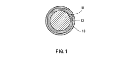
- FIG. 1 is a cross-sectional view showing conductive particles in the present embodiment.
- the electroconductive particle shown as a specific example of this invention has a resin particle, the electroless metal plating layer which coat
- FIG. 1 is a cross-sectional view showing an example of conductive particles in the present embodiment.
- the conductive particles include resin particles 11, an electroless metal plating layer 12 that covers the surface of the resin particles 11, and a metal sputter layer 13 that covers the electroless metal plating layer 12.
- Resin particle 11 is a base material (core) particle of conductive particles, and a particle that does not cause changes such as breakage, melting, flow, decomposition, and carbonization during mounting is used.
- resin particles 11 include monofunctional vinyl compounds typified by (meth) acrylic acid esters such as ethylene, propylene, and styrene, diallyl phthalate, triallyl trimellitate, triallyl cyanurate, Copolymers with polyfunctional vinyl compounds such as divinylbenzene, di (meth) acrylate, tri (meth) acrylates, curable polyurethane resin, cured epoxy resin, phenol resin, benzoguanamine resin, melamine resin, polyamide, polyimide , Silicone resin, fluororesin, polyester, polyphenylene sulfide resin, polyphenylene ether and the like.
- Particularly desirable resin particles 11 are selected from physical properties such as elastic modulus at the time of thermocompression bonding and fracture strength, and are polystyrene resin, acrylate resin, benzoguanamine resin, and a copolymer of a monofunctional vinyl compound and a polyfunctional vinyl compound.
- the average particle diameter of the resin particles 11 is not particularly limited, but is preferably 1 to 20 ⁇ m. When the average particle size is less than 1 ⁇ m, for example, when performing electroless plating, the particles tend to aggregate and hardly form single particles. On the other hand, if the average particle diameter exceeds 20 ⁇ m, the range used for fine pitch circuit boards as an anisotropic conductive material may be exceeded.
- the average particle diameter of the resin particles is obtained by measuring the particle diameters of 50 randomly selected base particles and arithmetically averaging them.
- the electroless metal plating layer 12 is one or more types of metal layers made of Cu, Ni, Co, Au, Ag, and Sn by electroless plating.
- an electroless Ni plating layer having good adhesion to the surface of the resin particles 11 is used.
- the thickness of the electroless metal plating layer 12 is preferably 20 to 200 nm. If the thickness is less than 20 nm, adhesion to the surface of the resin particles 11 cannot be obtained. On the other hand, if the thickness exceeds 200 nm, the conductive particles themselves aggregate and cannot be applied to fine pitch circuit connection.
- the metal sputter layer 13 is a metal layer made of Ni, Ru, W, Pd, Ir, Co, Mo, Ti, Rh, Pt, or an alloy containing one or more of these by sputtering.
- a bipolar sputtering method, a magnetron sputtering method, an RF (radio frequency) sputtering method, a reactive sputtering method, and other known sputtering methods can be widely used.
- a film forming method by a general vapor deposition method such as vacuum vapor deposition, laser ablation, chemical vapor deposition may be used.
- the Vickers hardness (Hv) of the metal sputter layer 13 is preferably 40 to 500. When the Vickers hardness (Hv) is less than 40, there is little biting into the wiring, and good connection resistance cannot be obtained. On the other hand, when the Vickers hardness (Hv) exceeds 500, the film ductility is poor, plating peeling does not occur, and good connection resistance cannot be obtained. In addition, Vickers hardness can be measured by the Vickers hardness test method prescribed
- the thickness of the metal sputter layer 13 is preferably 5 to 200 nm. When the thickness is less than 5 nm, a film is not uniformly formed, so that good connection resistance cannot be obtained. On the other hand, if the thickness exceeds 200 nm, the rate at which particle agglomeration occurs increases, which may reduce the insulating properties. Considering the manufacturing cost by sputtering, the more preferable thickness of the sputtered metal layer 13 is 5 to 30 nm.
- conductive particles use resin particles 11 as base material particles, the particle size distribution is narrower than that of metal particles, and can correspond to fine pitch wiring. Moreover, since the surface of the resin particle 11 is covered with the electroless metal plating layer 12, the adhesion with the surface of the resin particle 11 is improved, and the adhesion of the metal sputter layer 13 can be improved. Furthermore, since the sputtered metal layer 13 is formed as the outermost layer, the conductive particles can be caused to penetrate into the wiring, and the surface is smooth, such as IZO (Indium Zinc Oxide) or non-crystalline ITO (Indium Tin Oxide). Even when a fine pitch wiring material is used, high connection reliability can be obtained. Furthermore, the same effect can be obtained even when a metal wiring that easily forms an oxide film is used.
- IZO Indium Zinc Oxide
- ITO Indium Tin Oxide
- Anisotropic Conductive Material An anisotropic conductive material shown as a specific example of the present invention is obtained by dispersing the above-described conductive particles in a binder resin.
- Binder resin adhesive materials include epoxy resin, phenol resin, isocyanate resin, silicone resin, polyester resin, phenoxy resin, terpene resin, rosin resin, polyacrylic resin, styrene-butadiene rubber, acrylonitrile butadiene rubber, fluoro rubber, Thermosetting resins or thermoplastic resins such as polyethylene resin, vinyl resin, polybutylene resin, polybutadiene resin, polystyrene resin, polycarbonate resin, polyurethane resin, ionomer resin, polyacetal resin, etc. may be mentioned. You may use in combination of more than one kind.
- binder resin it is preferable to contain a film-forming resin, a thermosetting resin, and a curing agent.
- the film-forming resin corresponds to a high molecular weight resin having an average molecular weight of 10,000 or more, and preferably has an average molecular weight of about 10,000 to 80,000 from the viewpoint of film formation.
- the film forming resin include various resins such as phenoxy resin, polyester urethane resin, polyester resin, polyurethane resin, acrylic resin, polyimide resin, butyral resin, and these may be used alone or in combination of two or more. You may use it in combination.
- phenoxy resin is preferably used from the viewpoints of film formation state, connection reliability, and the like.
- thermosetting resin an epoxy resin, a liquid epoxy resin having fluidity at room temperature, or the like may be used alone, or two or more kinds may be mixed and used.
- the epoxy resin include bisphenol A type epoxy resin, bisphenol F type epoxy resin, novolac type epoxy resin, and various modified epoxy resins such as rubber and urethane. These may be used alone or in combination of two or more. Also good.
- Liquid epoxy resins include bisphenol type epoxy resin, naphthalene type epoxy resin, biphenyl type epoxy resin, phenol novolac type epoxy resin, stilbene type epoxy resin, triphenolmethane type epoxy resin, phenol aralkyl type epoxy resin, and naphthol type epoxy resin. Resin, dicyclopentadiene type epoxy resin, triphenylmethane type epoxy resin and the like can be used, and these may be used alone or in combination of two or more.
- the curing agent is not particularly limited and can be appropriately selected depending on the purpose.
- a latent curing agent that is activated by heating a latent curing agent that generates free radicals by heating, or the like can be used.
- the latent curing agent that is activated by heating include anionic curing agents such as polyamines and imidazoles, and cationic curing agents such as sulfonium salts.
- silane coupling agent epoxy, amino, mercapto sulfide, ureido, and the like can be used. Among these, in this Embodiment, an epoxy-type silane coupling agent is used preferably. Thereby, the adhesiveness in the interface of an organic material and an inorganic material can be improved. Moreover, you may add an inorganic filler. As the inorganic filler, silica, talc, titanium oxide, calcium carbonate, magnesium oxide and the like can be used, and the kind of the inorganic filler is not particularly limited. Depending on the content of the inorganic filler, the fluidity can be controlled and the particle capture rate can be improved.
- a rubber component or the like can also be used as appropriate for the purpose of relaxing the stress of the bonded body. Moreover, when mix
- a composition of a binder resin in which each component is blended is applied onto a release substrate using a bar coater, a coating device, etc., and the composition on the release substrate is then heated in a heat oven. Then, an anisotropic conductive film having a predetermined thickness is obtained by drying using a heat drying apparatus or the like.
- the release substrate has, for example, a laminated structure in which a release agent such as silicone is applied to PET (Poly Ethylene Terephthalate), OPP (Oriented Polypropylene), PMP (Poly-4-methylpentene-1), PTFE (Polytetrafluoroethylene), etc. While preventing the anisotropic conductive film from drying, these shapes are maintained.
- connection structure is such that the first electronic component and the second electronic component are electrically connected by the conductive particles described above.
- Examples of the first electronic component include an IC (Integrated Circuit) in which fine pitch bumps are formed.
- Examples of the second electronic component include IZO (Indium Zinc Oxide), amorphous ITO (Indium Tin Oxide), and the like.
- a fine-pitch wiring material having a smooth surface can be used.
- the conductive particles in the present embodiment are suitably used for joining such fine pitch IC and the wiring material. Since the conductive particles in the present embodiment cover the surface of the resin particles 11 with the electroless metal plating layer 12, the adhesion to the surface of the resin particles 11 is improved, and the adhesion of the metal sputter layer 13 is also improved. Can be improved. In addition, since the metal sputter layer 13 is formed as the outermost layer, conductive particles can be bitten into the wiring. For example, IZO (Indium Zinc Oxide), amorphous ITO (Indium Tin Oxide), etc. Even when a wiring material having a pitch is used, high connection reliability can be obtained. Furthermore, the same effect can be obtained even when a metal wiring that easily forms an oxide film is used.
- the method for connecting an electronic component in the present embodiment includes a resin particle, an electroless metal plating layer covering the surface of the resin particle, and a metal sputter layer excluding Au forming the outermost layer.
- An anisotropic conductive film in which particles are dispersed in a binder resin is pasted on a terminal of the first electronic component, a second electronic component is temporarily placed on the anisotropic conductive film, and heating is performed from the second electronic component. Pressing with a pressing device connects the terminal of the first electronic component and the terminal of the second electronic component. Thereby, the connection body by which the terminal of the 1st electronic component and the terminal of the 2nd electronic component were connected via the electroconductive particle is obtained.
- the anisotropic conductive film contains conductive particles whose resin particle surfaces are coated with an electroless metal plating layer, the conductive particles can be caused to bite into the wiring.
- high connection reliability can be obtained even when a fine pitch wiring material having a smooth surface such as IZO (Indium Zinc ⁇ Oxide) or amorphous ITO (Indium Tin Oxide) is used.
- IZO Indium Zinc ⁇ Oxide
- ITO Indium Tin Oxide
- Example> Examples of the present invention will be described below, but the present invention is not limited to these examples.
- the first metal layer and the second metal layer were formed in this order on the resin particles to produce conductive particles of Examples 1 to 10 and Comparative Examples 1 to 7.
- the thickness of the first metal layer, the thickness of the second metal layer, and the Vickers hardness (Hv) of the second metal layer were measured.
- anisotropic conductive films were produced using the conductive particles of Examples 1 to 10 and Comparative Examples 1 to 7. Using each anisotropic conductive film, an IC (Integrated Circuit) and a glass substrate on which a wiring pattern was formed were joined to obtain a mounting body. And about each mounting body, connection resistance was measured and connection reliability was evaluated.
- IC Integrated Circuit
- the thickness measurement of the metal layer was performed as follows.
- a metal of the second metal layer was formed on the glass substrate by a DC magnetron sputtering method.
- the sputtered metal layer was measured with a Vickers hardness tester (manufactured by Mitutoyo Corporation, HM-125) according to JIS Z2244, and this was defined as the Vickers hardness (Hv) of the second metal layer.
- this Vickers hardness (Hv) was computed by making test load into Kgf unit.
- phenoxy resin trade name: PKHH, manufactured by Phenoxy Associates
- naphthalene type bifunctional epoxy resin trade name: HP4032D, manufactured by DIC
- thermosetting resin 33 parts by mass of an imidazole curing agent (HP3941, manufactured by Asahi Kasei Chemicals Corporation)
- an epoxy silane coupling agent trade name: A-187, Momentive Performance Materials Co., Ltd.
- Conductive particles were prepared as in Examples 1 to 10 and Comparative Examples 1 to 7 described later.
- ITO Indium Tin Oxide
- the 0.7 mm thick ITO wiring board or glass substrate was bonded to a 0.7 mm thick IZO wiring board obtained by patterning an IZO (Indium Zinc Oxide) film.
- An anisotropic conductive film was slit to a predetermined width and attached to an ITO wiring board or an IZO wiring board. After temporarily fixing the IC thereon, bonding was performed at a bonding condition of 200 ° C.-60 MPa-5 sec using a heat tool coated with Teflon (trademark) having a thickness of 50 ⁇ m as a buffer material, thereby completing a mounting body. .
- connection resistance With respect to the mounted body, an initial resistance and a resistance after a TH test (Thermal Humidity Test) at a temperature of 85 ° C., a humidity of 85% RH, and 500 hours were measured. The measurement was performed using a digital multimeter (digital multimeter 7555, manufactured by Yokogawa Electric Corporation) to measure the connection resistance when a current of 1 mA was passed by the four-terminal method.
- Example 1 A Ni sputter layer (second metal layer) was formed by DC magnetron sputtering on the surface of the Ni-plated resin particles having an average particle diameter of 3 ⁇ m obtained by electroless Ni plating (first metal layer) on the resin particles.
- the Ni plating resin particles were prepared as follows. A palladium catalyst is supported by 5 g of divinylbenzene resin particles having an average particle diameter of 3 ⁇ m synthesized as described above by a dipping method. Nickel sulfate hexahydrate, sodium hypophosphite, sodium citrate are supported on the resin particles.
- Electroless nickel plating was performed using an electroless nickel plating solution (pH 12, plating temperature 50 ° C.) prepared from triethanolamine and thallium nitrate, and a Ni plating layer (first metal layer) was formed on the surface.
- Conductive particles were produced.
- a DC magnetron sputtering device manufactured in-house on the conductive particles having the Ni plating layer (first metal layer) formed on the surface, a vacuum degree of 1.5 Pa, an argon gas flow rate of 15.0 sccm, A second metal layer was formed on the surface of the first metal layer at a sputtering output of 1 W / cm 2 .
- the second metal layer was formed on the surface of the first metal layer while cooling the container holding the particles with a coolant having a temperature of 25 ° C.
- the thickness of the first metal layer was 100 nm, and the thickness of the second metal layer was 15 nm.
- the Vickers hardness (Hv) of the second metal layer was 50 to 70.
- Example 2 A Ru sputtered layer (second metal layer) is formed by DC magnetron sputtering on the surface of Ni-plated resin particles having an average particle diameter of 3 ⁇ m as in Example 1 in which electroless Ni plating (first metal layer) is applied to the resin particles. ) was formed.
- the thickness of the first metal layer was 100 nm, and the thickness of the second metal layer was 30 nm.
- the Vickers hardness (Hv) of the second metal layer was 300 to 400.
- Example 3 A Ru sputtered layer (second metal layer) is formed by DC magnetron sputtering on the surface of Ni-plated resin particles having an average particle diameter of 3 ⁇ m as in Example 1 in which electroless Ni plating (first metal layer) is applied to the resin particles. ) was formed.
- the thickness of the first metal layer was 100 nm, and the thickness of the second metal layer was 15 nm.
- the Vickers hardness (Hv) of the second metal layer was 300 to 400.
- Example 4 A Ru sputtered layer (second metal layer) is formed by DC magnetron sputtering on the surface of Ni-plated resin particles having an average particle diameter of 3 ⁇ m as in Example 1 in which electroless Ni plating (first metal layer) is applied to the resin particles. ) was formed.
- the thickness of the first metal layer was 100 nm, and the thickness of the second metal layer was 5 nm.
- the Vickers hardness (Hv) of the second metal layer was 300 to 400.
- Example 5 A Ru—Co sputtered layer (second layer) is formed on the surface of Ni-plated resin particles having an average particle diameter of 3 ⁇ m similar to Example 1 in which electroless Ni plating (first metal layer) is applied to resin particles by DC magnetron sputtering. Metal layer).
- the thickness of the first metal layer was 100 nm, and the thickness of the second metal layer was 15 nm.
- the Vickers hardness (Hv) of the second metal layer was 350 to 450.
- Example 6 The W sputtered layer (second metal layer) is formed on the surface of the Ni-plated resin particles having an average particle diameter of 3 ⁇ m similar to Example 1 in which the electroless Ni plating (first metal layer) is applied to the resin particles by the DC magnetron sputtering method. ) was formed.
- the thickness of the first metal layer was 100 nm, and the thickness of the second metal layer was 15 nm.
- the Vickers hardness (Hv) of the second metal layer was 300 to 400.
- the initial resistance was 0.1 ⁇ , and the resistance after the TH test was 1.6 ⁇ . Further, when the IC and the IZO wiring board were joined using the anisotropic conductive film containing the conductive particles, the initial resistance was 0.2 ⁇ , and the resistance after the TH test was 10.8 ⁇ . Table 1 shows the measurement results.
- Example 7 A Pd sputter layer (second metal layer) is formed by DC magnetron sputtering on the surface of Ni-plated resin particles having an average particle diameter of 3 ⁇ m similar to Example 1 in which electroless Ni plating (first metal layer) is applied to the resin particles. ) was formed.
- the thickness of the first metal layer was 100 nm, and the thickness of the second metal layer was 15 nm.
- the Vickers hardness (Hv) of the second metal layer was 40-60.
- Example 8 An Ir sputter layer (second metal layer) is formed by DC magnetron sputtering on the surface of Ni-plated resin particles having an average particle diameter of 3 ⁇ m similar to Example 1 in which electroless Ni plating (first metal layer) is applied to the resin particles. ) was formed.
- the thickness of the first metal layer was 100 nm, and the thickness of the second metal layer was 15 nm.
- the Vickers hardness (Hv) of the second metal layer was 300 to 400.
- Example 9 A Co sputtered layer (second metal layer) is formed on the surface of the Ni-plated resin particles having an average particle diameter of 3 ⁇ m similar to Example 1 in which electroless Ni plating (first metal layer) is applied to the resin particles by DC magnetron sputtering. ) was formed.
- the thickness of the first metal layer was 100 nm, and the thickness of the second metal layer was 15 nm.
- the Vickers hardness (Hv) of the second metal layer was 100 to 150.
- Example 10 A Mo sputtered layer (second metal layer) is formed by DC magnetron sputtering on the surface of Ni-plated resin particles having an average particle diameter of 3 ⁇ m as in Example 1 in which electroless Ni plating (first metal layer) is applied to the resin particles. ) was formed.
- the thickness of the first metal layer was 100 nm, and the thickness of the second metal layer was 15 nm.
- the Vickers hardness (Hv) of the second metal layer was 150 to 200.
- the thickness of the first metal layer was 100 nm, and the thickness of the second metal layer was 15 nm.
- the Vickers hardness (Hv) of the second metal layer was 10-30.
- the initial resistance was 0.1 ⁇ , and the resistance after the TH test was 3.0 ⁇ . Further, when the IC and the IZO wiring board were joined using the anisotropic conductive film containing the conductive particles, the initial resistance was 4.4 ⁇ , and the resistance after the TH test was 229.0 ⁇ . Table 2 shows the measurement results.
- Electroless Ni-P plating layer (first electrode layer) is formed on the surface of Ni-plated resin particles having an average particle diameter of 3 ⁇ m similar to Example 1 in which electroless Ni plating (first metal layer) is applied to resin particles by electroless plating. 2 metal layers).
- the thickness of the first metal layer was 100 nm, and the thickness of the second metal layer was 15 nm.
- the Vickers hardness (Hv) of the second metal layer was 10-30.
- the initial resistance was 0.1 ⁇ , and the resistance after the TH test was 4.1 ⁇ . Further, when the IC and the IZO wiring board were joined using the anisotropic conductive film containing the conductive particles, the initial resistance was 0.2 ⁇ , and the resistance after the TH test was 34.2 ⁇ . Table 2 shows the measurement results.
- the second metal layer was not formed using Ni-plated resin particles having an average particle diameter of 3 ⁇ m as in Example 1 in which electroless Ni plating (first metal layer) was applied to the resin particles.
- the thickness of the first metal layer was 100 nm.
- the Vickers hardness (Hv) of the first metal layer was 10-30.
- the initial resistance was 0.1 ⁇ , and the resistance after the TH test was 4.1 ⁇ . Further, when the IC and the IZO wiring board were joined using the anisotropic conductive film containing the conductive particles, the initial resistance was 0.2 ⁇ , and the resistance after the TH test was 34.2 ⁇ . Table 2 shows the measurement results.
- a Ni sputter layer (first metal layer) was formed on the surface of divinylbenzene resin particles having an average particle diameter of 3 ⁇ m by a DC magnetron sputtering method, and a second metal layer was not formed.
- the thickness of the first metal layer was 100 nm.
- the Vickers hardness (Hv) of the first metal layer was 50 to 70.
- the initial resistance was 0.1 ⁇ , and the resistance after the TH test was 5.8 ⁇ . Further, when the IC and the IZO wiring board were joined using the anisotropic conductive film containing the conductive particles, the initial resistance was 0.2 ⁇ , and the resistance after the TH test was 108.0 ⁇ . Table 2 shows the measurement results.
- a Ni sputtered layer (first metal layer) is formed by DC magnetron sputtering on the surface of divinylbenzene resin particles having an average particle diameter of 3 ⁇ m, and a Ni sputtered layer (second metal layer) is further formed by DC magnetron sputtering. did.
- the thickness of the first metal layer was 100 nm, and the thickness of the second metal layer was 15 nm.
- the Vickers hardness (Hv) of the first metal layer was 50 to 70.
- the initial resistance was 0.1 ⁇ , and the resistance after the TH test was 5.8 ⁇ . Further, when the IC and the IZO wiring board were joined using the anisotropic conductive film containing the conductive particles, the initial resistance was 0.2 ⁇ , and the resistance after the TH test was 108.0 ⁇ . Table 2 shows the measurement results.
- a Ni sputtered layer (first metal layer) is formed by DC magnetron sputtering on the surface of divinylbenzene resin particles having an average particle size of 3 ⁇ m, and an electroless Ni plated layer (first electroplating layer is formed on the surface of the Ni sputtered layer by electroless plating. 2 metal layers).
- the thickness of the first metal layer was 15 nm, and the thickness of the second metal layer was 100 nm.
- the Vickers hardness (Hv) of the first metal layer was 10-30.
- the initial resistance was 0.1 ⁇ , and the resistance after the TH test was 6.7 ⁇ . Further, when the IC and the IZO wiring board were joined using the anisotropic conductive film containing the conductive particles, the initial resistance was 0.2 ⁇ , and the resistance after the TH test was 67.8 ⁇ . Table 2 shows the measurement results.
- the thickness of the first metal layer was 100 nm, and the thickness of the second metal layer was 15 nm. Further, the Vickers hardness (Hv) of the first metal layer was 10 to 20.
- the first metal layer is an electroless metal plating layer
- the second metal layer is a Ni sputter layer, Ru sputter layer, Ru—Co sputter layer, W sputter layer, Pd.
- Good connection reliability was obtained by using any one of the sputtered layer, Ir sputtered layer, Co sputtered layer, and Mo sputtered layer.
- the Vickers hardness (Hv) of the second metal layer is 40 or more, good connection reliability is obtained, and in particular, the Vickers hardness (Hv) is 300 or more. In this case, good connection reliability was obtained for the IZO wiring board.
- good connection reliability was obtained when the thickness of the metal sputter layer was 5 to 30 nm.
Landscapes
- Wire Bonding (AREA)
- Conductive Materials (AREA)
- Non-Insulated Conductors (AREA)
- Electric Connection Of Electric Components To Printed Circuits (AREA)
Abstract
微細回路における接続信頼性を向上させる導電性粒子及びこれを用いた異方性導電材料を提供する。樹脂粒子(11)と、樹脂粒子表面を被覆する無電解金属めっき層(12)と、最外層を形成するAuを除く金属スパッタ層(13)とを有する導電性粒子を用いる。最外層に硬い金属スパッタ層(13)が形成されているため、配線へ導電性粒子を食い込ませることができ、高い接続信頼性を得ることができる。
Description
本発明は、電極間の接続に用いられる導電性粒子及びこれを用いた異方性導電材料に関する。本出願は、日本国において2011年2月4日に出願された日本特許出願番号特願2011-022451を基礎として優先権を主張するものであり、この出願を参照することにより、本出願に援用される。
従来、異方性導電フィルム(ACF:Anisotropic Conductive Film)は、プリント基板に半導体などの部品を装着させるために使用されている。例えば、LCD(Liquid Crystal Display)パネルの製造においては、画素をコントロールする駆動IC(集積回路)をガラス基板に接合する、いわゆるチップ・オン・グラス(COG)などに用いられている。異方性導電フィルムに分散される導電性粒子としては、樹脂粒子の周りに無電解Niめっきを施し、その外周にAuめっきが施されたものが知られている。
近年、IZO(Indium Zinc Oxide)、非結晶ITO(Indium Tin Oxide)など、透過度が高く、表面が平滑な配線材が使用されている。このため、金属めっきにより被膜された硬度の低い導電性粒子では、導電性粒子が配線材に食い込まず、良好な接続信頼性が得られないことがある。一方、スパッタリングなどの真空蒸着法により金属が被膜された硬度が高い導電性粒子によれば、接続信頼性の向上が期待される。
しかしながら、特許文献1、2に記載された導電性粒子のように、樹脂粒子表面に直接スパッタリングにより金属を積層させたものは、樹脂コア粒子表面とスパッタ金属表面との密着性が悪く、特に表面平滑性を有する配線材を使用した場合、接続信頼性が悪化してしまう。
また、特許文献3には、母材粒子に金属粒子を用い、金属粒子表面にスパッタ金属を積層させた導電性粒子が記載されているが、金属粒子は、樹脂粒子に比べ粒度分布が幅広いため、ファインピッチの回路に対応することが困難である。
本発明は、このような従来の実情に鑑みて提案されたものであり、微細回路における接続信頼性を向上させる導電性粒子及びこれを用いた異方性導電材料を提供する。
本件発明者らは、鋭意検討を行った結果、樹脂粒子表面に無電解金属めっきを被覆することにより、樹脂粒子表面との密着性を向上させ、最外層を金属スパッタ層とすることにより、良好な接続信頼性が得られることを見出した。
すなわち、本発明に係る導電性粒子は、樹脂粒子と、前記樹脂粒子表面を被覆する無電解金属めっき層と、最外層を形成するAuを除く金属スパッタ層とを有することを特徴とする。
また、本発明に係る異方性導電材料は、バインダ樹脂と、前記バインダ樹脂に分散された導電性粒子とを備え、前記導電性粒子は、樹脂粒子と、前記樹脂粒子表面を被覆する無電解金属めっき層と、最外層を形成するAuを除く金属スパッタ層とを有することを特徴とする。
また、本発明に係る接続構造体は、第1の電子部品と第2の電子部品とが、樹脂粒子と、前記樹脂粒子表面を被覆する無電解金属めっき層と、最外層を形成するAuを除く金属スパッタ層とを有する導電性粒子によって電気的に接続されていることを特徴とする。
また、本発明に係る接続方法は、樹脂粒子と、前記樹脂粒子表面を被覆する無電解金属めっき層と、最外層を形成するAuを除く金属スパッタ層とを有する導電性粒子がバインダ樹脂に分散された異方性導電フィルムを第1の電子部品の端子上に貼付け、前記異方性導電フィルム上に第2の電子部品を仮配置させ、前記第2の電子部品上から加熱押圧装置により押圧し、前記第1の電子部品の端子と、前記第2の電子部品の端子とを接続させることを特徴とする。
本発明によれば、樹脂粒子表面に無電解金属めっきを被覆することにより、樹脂粒子表面との密着性を向上させ、最外層を金属スパッタ層とすることにより、例えばIZO(Indium Zinc Oxide)、非結晶ITO(Indium Tin Oxide)など、表面が平滑なファインピッチの配線材を使用した場合でも、高い接続信頼性を得ることができる。更に、酸化膜を形成し易い金属配線を用いた場合にも、同様な効果を得ることができる。
以下、本発明の実施の形態について、図面を参照しながら下記順序にて詳細に説明する。
1.導電性粒子
2.異方性導電材料
3.接続構造体
4.実施例
1.導電性粒子
2.異方性導電材料
3.接続構造体
4.実施例
<1.導電性粒子>
本発明の具体例として示す導電性粒子は、樹脂粒子と、樹脂粒子表面を被覆する無電解金属めっき層と、最外層を形成するAuを除く金属スパッタ層とを有するものである。なお、本発明の目的を損なわない範囲で、樹脂粒子表面を被覆する無電解金属めっき層と、最外層を形成する金属スパッタ層との間に、無電解金属めっき層又は金属スパッタ層を設けても構わない。
本発明の具体例として示す導電性粒子は、樹脂粒子と、樹脂粒子表面を被覆する無電解金属めっき層と、最外層を形成するAuを除く金属スパッタ層とを有するものである。なお、本発明の目的を損なわない範囲で、樹脂粒子表面を被覆する無電解金属めっき層と、最外層を形成する金属スパッタ層との間に、無電解金属めっき層又は金属スパッタ層を設けても構わない。
図1は、本実施の形態における導電性粒子の一例を示す断面図である。この導電性粒子は、樹脂粒子11と、樹脂粒子11表面を被覆する無電解金属めっき層12と、無電解金属めっき層12を被覆する金属スパッタ層13とを有する。
樹脂粒子11は、導電性粒子の母材(コア)粒子であり、実装時に破壊、融解、流動、分解、炭化などの変化を起こさないものが用いられる。このような樹脂粒子11としては、例えば、エチレン、プロピレン、スチレンなどの(メタ)アクリル酸エステル類に代表される単官能のビニル化合物と、ジアリルフタレート、トリアリルトリメリテート、トリアリルシアヌレート、ジビニルベンゼン、ジ(メタ)アクリレート、トリ(メタ)アクリレート類などの多官能ビニル化合物との共重合体、硬化性ポリウレタン樹脂、硬化エポキシ樹脂、フェノール樹脂、ペンゾグアナミン樹脂、メラミン樹脂、ポリアミド、ポリイミド、シリコーン樹脂、フッ素樹脂、ポリエステル、ポリフェニレンスルフィド樹脂、ポリフェニレンエーテルなどが挙げられる。特に望ましい樹脂粒子11は、熱圧着時の弾性率、破壊強度といった物性から選定され、ポリスチレン樹脂、アクリル酸エステル樹脂、ベンゾグアナミン樹脂、単官能ビニル化合物と多官能ビニル化合物との共重合体である。
樹脂粒子11の平均粒径は、特に限定されないが、1~20μmであることが好ましい。平均粒径が1μm未満であると、例えば、無電解めっきをする際に凝集しやすく、単粒子となり難い。一方、平均粒径が20μmを超えると、異方性導電材料としてファインピッチの回路基板などに用いられる範囲を超えることがある。なお、樹脂粒子の平均粒子径は、無作為に選んだ50個の基材微粒子について粒子径を測定し、これらを算術平均したものである。
無電解金属めっき層12は、無電解めっきにより、Cu、Ni、Co、Au、Ag、Snからなる1種または複数種の金属層である。好ましい無電解金属めっき層12としては、樹脂粒子11表面との密着性が良好な無電解Niめっき層が用いられる。
無電解金属めっき層12の厚さは、20~200nmであることが好ましい。厚さが20nm未満であると、樹脂粒子11表面との密着性が得られない。一方、厚さが200nmを超えると、導電性粒子自体が凝集し、ファインピッチな回路接続に適用できない。
金属スパッタ層13は、スパッタリング法により、Ni、Ru、W、Pd、Ir、Co、Mo、Ti、Rh、Pt、又はこれらの1種以上を含む合金からなる金属層である。スパッタリング法としては、二極スパッタリング法、マグネトロンスパッタリング法、RF(高周波)スパッタリング法、反応性スパッタリング法、その他公知のスパッタリング法を広く利用することができる。また、金属スパッタ層13に所定の硬さが得られるのであれば、真空蒸着、レーザーアブレーション、化学的気相成長などの一般的な気相成長法による皮膜形成法を用いても構わない。
金属スパッタ層13のビッカース硬さ(Hv)は、40~500であることが好ましい。ビッカース硬さ(Hv)が40未満であると、配線への食い込みが少なく、良好な接続抵抗を得ることができない。一方、ビッカース硬さ(Hv)が500を超えると、皮膜延性が乏しく、めっき剥がれが発生していまい、良好な接続抵抗を得ることができない。なお、ビッカース硬さは、JISZ2244で規定されるビッカース硬さ試験法により測定することができる。
金属スパッタ層13の厚さは、5~200nmであることが好ましい。厚さが5nm未満であると、皮膜が均一に生成されないため、良好な接続抵抗が得られない。一方、厚さが200nmを超えると、粒子凝集が発生する割合が高くなり、絶縁性が低下する虞がある。スパッタリングによる製造コストを考慮すると、より好ましい金属スパッタ層13の厚さは、5~30nmである。
このような導電性粒子は、母材粒子として樹脂粒子11を用いるため、金属粒子に比べ粒度分布が狭く、ファインピッチ化された配線にも対応することができる。また、樹脂粒子11表面を無電解金属めっき層12で被覆するため、樹脂粒子11表面との密着性が向上し、また、金属スパッタ層13の密着性も向上させることができる。さらに、最外層として金属スパッタ層13が形成されているため、配線へ導電性粒子を食い込ませることができ、例えばIZO(Indium Zinc Oxide)、非結晶ITO(Indium Tin Oxide)など、表面が平滑なファインピッチの配線材を使用した場合でも、高い接続信頼性を得ることができる。更に、酸化膜を形成し易い金属配線を用いた場合にも、同様な効果を得ることができる。
<2.異方性導電材料>
本発明の具体例として示す異方性導電材料は、上述した導電性粒子がバインダ樹脂に分散されたものである。
本発明の具体例として示す異方性導電材料は、上述した導電性粒子がバインダ樹脂に分散されたものである。
バインダ樹脂の接着性材料としては、エポキシ樹脂、フェノール樹脂、イソシアネート樹脂、シリコーン樹脂、ポリエステル樹脂、フェノキシ樹脂、テルペン樹脂、ロジン樹脂、ポリアクリル樹脂、スチレン-ブタジエン系ゴム、アクリロニトリルブタジエンゴム、フッ素ゴム、ポリエチレン樹脂、ビニル樹脂、ポリブチレン樹脂、ポリブタジエン樹脂、ポリスチレン樹脂、ポリカーボネート樹脂、ポリウレタン樹脂、アイオノマー樹脂、ポリアセタール樹脂などの熱硬化性樹脂又は熱可塑性樹脂が挙げられ、これらは単独で使用しても、2種類以上組み合わせて使用してもよい。
具体的なバインダ樹脂としては、膜形成樹脂と、熱硬化性樹脂と、硬化剤とを含有することが好ましい。
膜形成樹脂は、平均分子量が10000以上の高分子量樹脂に相当し、フィルム形成性の観点から、10000~80000程度の平均分子量であることが好ましい。膜形成樹脂としては、フェノキシ樹脂、ポリエステルウレタン樹脂、ポリエステル樹脂、ポリウレタン樹脂、アクリル樹脂、ポリイミド樹脂、ブチラール樹脂などの種々の樹脂が挙げられ、これらは単独で用いても良いし、2種類以上を組み合わせて用いても良い。これらの中でも膜形成状態、接続信頼性などの観点からフェノキシ樹脂が好適に用いられる。
熱硬化性樹脂は、エポキシ樹脂、常温で流動性を有する液状エポキシ樹脂などを単独で用いても2種以上を混合して用いてもよい。エポキシ樹脂としては、ビスフェノールA型エポキシ樹脂、ビスフェノールF型エポキシ樹脂、ノボラック型エポキシ樹脂や、ゴム、ウレタンなどの各種変性エポキシ樹脂が例示され、これらは単独でも、2種以上を混合して用いてもよい。また、液状エポキシ樹脂としては、ビスフェノール型エポキシ樹脂、ナフタレン型エポキシ樹脂、ビフェニル型エポキシ樹脂、フェノールノボラック型エポキシ樹脂、スチルベン型エポキシ樹脂、トリフェノールメタン型エポキシ樹脂、フェノールアラルキル型エポキシ樹脂、ナフトール型エポキシ樹脂、ジシクロペンタジエン型エポキシ樹脂、トリフェニルメタン型エポキシ樹脂などを用いることができ、これらは単独でも、2種以上を混合して用いてもよい。
硬化剤は、特に制限はなく、目的に応じて適宜選択することができ、例えば、加熱により活性化する潜在性硬化剤、加熱により遊離ラジカルを発生させる潜在性硬化剤などを用いることができる。加熱により活性化する潜在性硬化剤としては、例えば、ポリアミン、イミダゾールなどのアニオン系硬化剤やスルホニウム塩などのカチオン系硬化剤などが挙げられる。
その他の添加組成物として、シランカップリング剤を添加することが好ましい。シランカップリング剤としては、エポキシ系、アミノ系、メルカプト・スルフィド系、ウレイド系などを用いることができる。これらの中でも、本実施の形態では、エポキシ系シランカップリング剤が好ましく用いられる。これにより、有機材料と無機材料の界面における接着性を向上させることができる。また、無機フィラーを添加させてもよい。無機フィラーとしては、シリカ、タルク、酸化チタン、炭酸カルシウム、酸化マグネシウムなどを用いることができ、無機フィラーの種類は特に限定されるものではない。無機フィラーの含有量により、流動性を制御し、粒子捕捉率を向上させることができる。また、ゴム成分なども接合体の応力を緩和させる目的で、適宜使用することができる。また、これらバインダ樹脂の各成分を配合する際には、トルエン、酢酸エチル、又はこれらの混合溶剤が好ましく用いられる。
異方性導電フィルムを作製する場合、各成分が配合されたバインダ樹脂の組成物をバーコーター、塗布装置などを用いて、剥離基材上に塗布し、剥離基材上の組成物を熱オーブン、加熱乾燥装置などを用いて乾燥させることにより、所定厚さの異方性導電フィルムを得る。剥離基材は、例えば、シリコーンなどの剥離剤がPET(Poly Ethylene Terephthalate)、OPP(Oriented Polypropylene)、PMP(Poly-4-methylpentene-1)、PTFE(Polytetrafluoroethylene)などに塗布した積層構造からなり、異方性導電フィルムの乾燥を防ぐとともに、これらの形状を維持する。
<3.接続構造体>
本発明の具体例として示す接続構造体は、第1の電子部品と第2の電子部品とが、上述した導電性粒子によって電気的に接続されているものである。
本発明の具体例として示す接続構造体は、第1の電子部品と第2の電子部品とが、上述した導電性粒子によって電気的に接続されているものである。
第1の電子部品としては、ファインピッチバンプが形成されたIC(Integrated Circuit)が挙げられ、第2の電子部品としては、例えばIZO(Indium Zinc Oxide)、非結晶ITO(Indium Tin Oxide)など、表面が平滑なファインピッチの配線材が挙げられる。
本実施の形態における導電性粒子は、このようなファインピッチ化されたICと配線材とを接合するのに好適に用いられる。本実施の形態における導電性粒子は、樹脂粒子11表面を無電解金属めっき層12で被覆しているため、樹脂粒子11表面との密着性を向上させ、また、金属スパッタ層13の密着性も向上させることができる。また、最外層として金属スパッタ層13が形成されるため、配線へ導電性粒子を食い込ませることができ、例えばIZO(Indium Zinc Oxide)、非結晶ITO(Indium Tin Oxide)など、表面が平滑なファインピッチの配線材を使用した場合でも、高い接続信頼性を得ることができる。更に、酸化膜を形成し易い金属配線を用いた場合にも、同様な効果を得ることができる。
次に、上述した異方性導電材料を用いた電子部品の接続方法について説明する。本実施の形態における電子部品の接続方法は、上述のように、樹脂粒子と、樹脂粒子表面を被覆する無電解金属めっき層と、最外層を形成するAuを除く金属スパッタ層とを有する導電性粒子がバインダ樹脂に分散された異方性導電フィルムを第1の電子部品の端子上に貼付け、異方性導電フィルム上に第2の電子部品を仮配置させ、第2の電子部品上から加熱押圧装置により押圧し、第1の電子部品の端子と、第2の電子部品の端子とを接続させるものである。これにより、導電性粒子を介して第1の電子部品の端子と第2の電子部品の端子とが接続された接続体が得られる。
本実施の形態における電子部品の接続方法は、異方性導電フィルムに樹脂粒子表面を無電解金属めっき層で被覆した導電性粒子を含有させているため、配線へ導電性粒子を食い込ませることができ、例えばIZO(Indium Zinc Oxide)、非結晶ITO(Indium Tin Oxide)など、表面が平滑なファインピッチの配線材を使用した場合でも、高い接続信頼性を得ることができる。更に、酸化膜を形成し易い金属配線を用いた場合にも、同様な効果を得ることができる。
<4.実施例>
以下、本発明の実施例について説明するが、本発明はこれらの実施例に限定されるものではない。
以下、本発明の実施例について説明するが、本発明はこれらの実施例に限定されるものではない。
先ず、樹脂粒子に第1の金属層と第2の金属層とをこの順に形成して実施例1~10及び比較例1~7の導電性粒子を作製した。各導電性粒子について、第1の金属層の厚さ、第2の金属層の厚さ、及び第2の金属層のビッカース硬さ(Hv)を測定した。
次に、実施例1~10及び比較例1~7の導電性粒子を用いて異方性導電フィルムを作製した。各異方性導電フィルムを用いてIC(Integrated Circuit)と配線パターンが形成されたガラス基板とを接合させ、実装体を得た。そして、各実装体について、接続抵抗を測定し、接続信頼性を評価した。
金属層の厚さ測定、金属層の硬さ測定、異方性導電フィルムの作製、実装体の作製、及び接続抵抗の測定は、次のように行った。
[金属層の厚さ測定]
エポキシ接着剤に導電性粒子を分散させて硬化させ、研磨機(丸本ストルアス社製)にて粒子断面を削り出した。この粒子断面をSEM(Scanning Electron Microscope)(キーエンス社製、VE-8800)にて観察し、第1の金属層の厚さ、及び第2の金属層の厚さを測定した。
エポキシ接着剤に導電性粒子を分散させて硬化させ、研磨機(丸本ストルアス社製)にて粒子断面を削り出した。この粒子断面をSEM(Scanning Electron Microscope)(キーエンス社製、VE-8800)にて観察し、第1の金属層の厚さ、及び第2の金属層の厚さを測定した。
[金属層の硬さ測定]
ガラス基板上に第2の金属層の金属をDCマグネトロンスパッタリング法により成膜した。この金属スパッタ層をビッカース硬さ試験機(ミツトヨ社製、HM-125)により、JIS Z2244に準拠して測定し、これを第2の金属層のビッカース硬さ(Hv)とした。なお、本ビッカース硬さ(Hv)は、試験荷重をKgf単位として算出した。
ガラス基板上に第2の金属層の金属をDCマグネトロンスパッタリング法により成膜した。この金属スパッタ層をビッカース硬さ試験機(ミツトヨ社製、HM-125)により、JIS Z2244に準拠して測定し、これを第2の金属層のビッカース硬さ(Hv)とした。なお、本ビッカース硬さ(Hv)は、試験荷重をKgf単位として算出した。
[異方性導電フィルムの作製]
膜形成樹脂として、フェノキシ樹脂(商品名:PKHH、フェノキシアソシエイツ社製)を25質量部、熱硬化性樹脂として、ナフタレン型2官能エポキシ樹脂(商品名:HP4032D、DIC社製)を10質量部、イミダゾール系硬化剤(HP3941、旭化成ケミカルズ社製(株))を33質量部、エポキシ系シランカップリング剤(商品名:A-187、モメンティブ・パフォーマンス・マテリアルズ(株))を2質量部、及び導電性粒子を30質量部配合し、樹脂組成物を調製した。この樹脂組成物を、剥離処理されたPETにバーコーターを用いて塗布し、70℃のオーブンで5分乾燥させ、厚さ20μmの異方性導電フィルムを作製した。導電性粒子は、後述する実施例1~10及び比較例1~7のようにそれぞれ作製した。
膜形成樹脂として、フェノキシ樹脂(商品名:PKHH、フェノキシアソシエイツ社製)を25質量部、熱硬化性樹脂として、ナフタレン型2官能エポキシ樹脂(商品名:HP4032D、DIC社製)を10質量部、イミダゾール系硬化剤(HP3941、旭化成ケミカルズ社製(株))を33質量部、エポキシ系シランカップリング剤(商品名:A-187、モメンティブ・パフォーマンス・マテリアルズ(株))を2質量部、及び導電性粒子を30質量部配合し、樹脂組成物を調製した。この樹脂組成物を、剥離処理されたPETにバーコーターを用いて塗布し、70℃のオーブンで5分乾燥させ、厚さ20μmの異方性導電フィルムを作製した。導電性粒子は、後述する実施例1~10及び比較例1~7のようにそれぞれ作製した。
[実装体の作製]
異方性導電フィルムを用いて、IC(1.8mm×20mm、t=0.5mm、Au-plated bump 30μm×85μm、h=15μm)と、ガラス基板にITO(Indium Tin Oxide)膜がパターンニングされた厚さ0.7mmのITO配線板又はガラス基板にIZO(Indium Zinc Oxide)膜がパターンニングされた厚さ0.7mmのIZO配線板との接合を行った。
異方性導電フィルムを用いて、IC(1.8mm×20mm、t=0.5mm、Au-plated bump 30μm×85μm、h=15μm)と、ガラス基板にITO(Indium Tin Oxide)膜がパターンニングされた厚さ0.7mmのITO配線板又はガラス基板にIZO(Indium Zinc Oxide)膜がパターンニングされた厚さ0.7mmのIZO配線板との接合を行った。
異方性導電フィルムを所定幅にスリットしてITO配線板又はIZO配線板に貼り付けた。その上にICを仮固定した後、緩衝材として厚さ50μmのテフロン(商標)が被覆されたヒートツールを用いて、接合条件200℃-60MPa-5secで接合を行い、実装体を完成させた。
[接続抵抗の測定]
実装体について、初期(Initial)の抵抗と、温度85℃、湿度85%RH、500時間のTHテスト(Thermal Humidity Test)後の抵抗を測定した。測定は、デジタルマルチメータ(デジタルマルチメータ7555、横河電機社製)を用いて4端子法にて電流1mAを流したときの接続抵抗を測定した。
実装体について、初期(Initial)の抵抗と、温度85℃、湿度85%RH、500時間のTHテスト(Thermal Humidity Test)後の抵抗を測定した。測定は、デジタルマルチメータ(デジタルマルチメータ7555、横河電機社製)を用いて4端子法にて電流1mAを流したときの接続抵抗を測定した。
[ジビニルベンゼン系樹脂粒子の作製]
ジビニルベンゼン、スチレン、ブチルメタクリレートの混合比を調整した溶液に、重合開始剤としてベンゾイルパーオキサイドを投入して高速で均一攪拌しながら加熱を行い、重合反応を行うことにより微粒子分散液を得た。前記微粒子分散液をろ過し減圧乾燥することにより微粒子の凝集体であるブロック体を得た。更に、前記ブロック体を粉砕することにより、平均粒子径3.0μmのジビニルベンゼン系樹脂粒子を得た。
ジビニルベンゼン、スチレン、ブチルメタクリレートの混合比を調整した溶液に、重合開始剤としてベンゾイルパーオキサイドを投入して高速で均一攪拌しながら加熱を行い、重合反応を行うことにより微粒子分散液を得た。前記微粒子分散液をろ過し減圧乾燥することにより微粒子の凝集体であるブロック体を得た。更に、前記ブロック体を粉砕することにより、平均粒子径3.0μmのジビニルベンゼン系樹脂粒子を得た。
[実施例1]
樹脂粒子に無電解Niめっき(第1の金属層)が施された平均粒径3μmのNiめっき樹脂粒子の表面にDCマグネトロンスパッタリング法によりNiスパッタ層(第2の金属層)を形成した。Niめっき樹脂粒子は次のように作製した。上述のように合成した平均粒径3μmのジビニルベンゼン系樹脂粒子5gに、パラジウム触媒を浸漬法により担持させ、この樹脂粒子に対し、硫酸ニッケル六水和物、次亜リン酸ナトリウム、クエン酸ナトリウム、トリエタノールアミン及び硝酸タリウムから調製された無電解ニッケルめっき液(pH12、メッキ液温50℃)を用いて無電解ニッケルめっきを行い、Niめっき層(第1金属層)が表面に形成された導電性粒子を作製した。上記により作成したNiめっき層(第1の金属層)が表面に形成された導電性粒子に、内製したDCマグネトロンスパッタ装置を使用して、真空度1.5Pa、アルゴンガス流量15.0sccm、スパッタリング出力1W/cm2にて、第1の金属層の表面に第2の金属層を形成した。粒子を保持する容器を温度25℃の冷媒にて冷却しながら、第1の金属層の表面に第2の金属層を形成した。
樹脂粒子に無電解Niめっき(第1の金属層)が施された平均粒径3μmのNiめっき樹脂粒子の表面にDCマグネトロンスパッタリング法によりNiスパッタ層(第2の金属層)を形成した。Niめっき樹脂粒子は次のように作製した。上述のように合成した平均粒径3μmのジビニルベンゼン系樹脂粒子5gに、パラジウム触媒を浸漬法により担持させ、この樹脂粒子に対し、硫酸ニッケル六水和物、次亜リン酸ナトリウム、クエン酸ナトリウム、トリエタノールアミン及び硝酸タリウムから調製された無電解ニッケルめっき液(pH12、メッキ液温50℃)を用いて無電解ニッケルめっきを行い、Niめっき層(第1金属層)が表面に形成された導電性粒子を作製した。上記により作成したNiめっき層(第1の金属層)が表面に形成された導電性粒子に、内製したDCマグネトロンスパッタ装置を使用して、真空度1.5Pa、アルゴンガス流量15.0sccm、スパッタリング出力1W/cm2にて、第1の金属層の表面に第2の金属層を形成した。粒子を保持する容器を温度25℃の冷媒にて冷却しながら、第1の金属層の表面に第2の金属層を形成した。
第1の金属層の厚さは100nmであり、第2の金属層の厚さは15nmであった。また、第2の金属層のビッカース硬さ(Hv)は、50~70であった。
この導電性粒子を含む異方性導電フィルム用いてICとITO配線板とを接合させたところ、初期抵抗は0.1Ω、THテスト後の抵抗は0.5Ωであった。また、この導電性粒子を含む異方性導電フィルム用いてICとIZO配線板とを接合させたところ、初期抵抗は0.1Ω、THテスト後の抵抗は11.1Ωであった。表1に、これらの測定結果を示す。
[実施例2]
樹脂粒子に無電解Niめっき(第1の金属層)が施された実施例1と同様の平均粒径3μmのNiめっき樹脂粒子の表面にDCマグネトロンスパッタリング法によりRuスパッタ層(第2の金属層)を形成した。
樹脂粒子に無電解Niめっき(第1の金属層)が施された実施例1と同様の平均粒径3μmのNiめっき樹脂粒子の表面にDCマグネトロンスパッタリング法によりRuスパッタ層(第2の金属層)を形成した。
第1の金属層の厚さは100nmであり、第2の金属層の厚さは30nmであった。また、第2の金属層のビッカース硬さ(Hv)は、300~400であった。
この導電性粒子を含む異方性導電フィルム用いてICとITO配線板とを接合させたところ、初期抵抗は0.1Ω、THテスト後の抵抗は0.4Ωであった。また、この導電性粒子を含む異方性導電フィルム用いてICとIZO配線板とを接合させたところ、初期抵抗は0.1Ω、THテスト後の抵抗は4.5Ωであった。表1に、これらの測定結果を示す。
[実施例3]
樹脂粒子に無電解Niめっき(第1の金属層)が施された実施例1と同様の平均粒径3μmのNiめっき樹脂粒子の表面にDCマグネトロンスパッタリング法によりRuスパッタ層(第2の金属層)を形成した。
樹脂粒子に無電解Niめっき(第1の金属層)が施された実施例1と同様の平均粒径3μmのNiめっき樹脂粒子の表面にDCマグネトロンスパッタリング法によりRuスパッタ層(第2の金属層)を形成した。
第1の金属層の厚さは100nmであり、第2の金属層の厚さは15nmであった。また、第2の金属層のビッカース硬さ(Hv)は、300~400であった。
この導電性粒子を含む異方性導電フィルム用いてICとITO配線板とを接合させたところ、初期抵抗は0.1Ω、THテスト後の抵抗は0.4Ωであった。また、この導電性粒子を含む異方性導電フィルム用いてICとIZO配線板とを接合させたところ、初期抵抗は0.1Ω、THテスト後の抵抗は4.2Ωであった。表1に、これらの測定結果を示す。
[実施例4]
樹脂粒子に無電解Niめっき(第1の金属層)が施された実施例1と同様の平均粒径3μmのNiめっき樹脂粒子の表面にDCマグネトロンスパッタリング法によりRuスパッタ層(第2の金属層)を形成した。
樹脂粒子に無電解Niめっき(第1の金属層)が施された実施例1と同様の平均粒径3μmのNiめっき樹脂粒子の表面にDCマグネトロンスパッタリング法によりRuスパッタ層(第2の金属層)を形成した。
第1の金属層の厚さは100nmであり、第2の金属層の厚さは5nmであった。また、第2の金属層のビッカース硬さ(Hv)は、300~400であった。
この導電性粒子を含む異方性導電フィルム用いてICとITO配線板とを接合させたところ、初期抵抗は0.1Ω、THテスト後の抵抗は1.1Ωであった。また、この導電性粒子を含む異方性導電フィルム用いてICとIZO配線板とを接合させたところ、初期抵抗は0.1Ω、THテスト後の抵抗は8.5Ωであった。表1に、これらの測定結果を示す。
[実施例5]
樹脂粒子に無電解Niめっき(第1の金属層)が施された実施例1と同様の平均粒径3μmのNiめっき樹脂粒子の表面にDCマグネトロンスパッタリング法によりRu-Coスパッタ層(第2の金属層)を形成した。
樹脂粒子に無電解Niめっき(第1の金属層)が施された実施例1と同様の平均粒径3μmのNiめっき樹脂粒子の表面にDCマグネトロンスパッタリング法によりRu-Coスパッタ層(第2の金属層)を形成した。
第1の金属層の厚さは100nmであり、第2の金属層の厚さは15nmであった。また、第2の金属層のビッカース硬さ(Hv)は、350~450であった。
この導電性粒子を含む異方性導電フィルム用いてICとITO配線板とを接合させたところ、初期抵抗は0.1Ω、THテスト後の抵抗は0.5Ωであった。また、この導電性粒子を含む異方性導電フィルム用いてICとIZO配線板とを接合させたところ、初期抵抗は0.1Ω、THテスト後の抵抗は3.2Ωであった。表1に、これらの測定結果を示す。
[実施例6]
樹脂粒子に無電解Niめっき(第1の金属層)が施された実施例1と同様の平均粒径3μmのNiめっき樹脂粒子の表面にDCマグネトロンスパッタリング法によりWスパッタ層(第2の金属層)を形成した。
樹脂粒子に無電解Niめっき(第1の金属層)が施された実施例1と同様の平均粒径3μmのNiめっき樹脂粒子の表面にDCマグネトロンスパッタリング法によりWスパッタ層(第2の金属層)を形成した。
第1の金属層の厚さは100nmであり、第2の金属層の厚さは15nmであった。また、第2の金属層のビッカース硬さ(Hv)は、300~400であった。
この導電性粒子を含む異方性導電フィルム用いてICとITO配線板とを接合させたところ、初期抵抗は0.1Ω、THテスト後の抵抗は1.6Ωであった。また、この導電性粒子を含む異方性導電フィルム用いてICとIZO配線板とを接合させたところ、初期抵抗は0.2Ω、THテスト後の抵抗は10.8Ωであった。表1に、これらの測定結果を示す。
[実施例7]
樹脂粒子に無電解Niめっき(第1の金属層)が施された実施例1と同様の平均粒径3μmのNiめっき樹脂粒子の表面にDCマグネトロンスパッタリング法によりPdスパッタ層(第2の金属層)を形成した。
樹脂粒子に無電解Niめっき(第1の金属層)が施された実施例1と同様の平均粒径3μmのNiめっき樹脂粒子の表面にDCマグネトロンスパッタリング法によりPdスパッタ層(第2の金属層)を形成した。
第1の金属層の厚さは100nmであり、第2の金属層の厚さは15nmであった。また、第2の金属層のビッカース硬さ(Hv)は、40~60であった。
この導電性粒子を含む異方性導電フィルム用いてICとITO配線板とを接合させたところ、初期抵抗は0.1Ω、THテスト後の抵抗は0.6Ωであった。また、この導電性粒子を含む異方性導電フィルム用いてICとIZO配線板とを接合させたところ、初期抵抗は0.1Ω、THテスト後の抵抗は22.8Ωであった。表1に、これらの測定結果を示す。
[実施例8]
樹脂粒子に無電解Niめっき(第1の金属層)が施された実施例1と同様の平均粒径3μmのNiめっき樹脂粒子の表面にDCマグネトロンスパッタリング法によりIrスパッタ層(第2の金属層)を形成した。
樹脂粒子に無電解Niめっき(第1の金属層)が施された実施例1と同様の平均粒径3μmのNiめっき樹脂粒子の表面にDCマグネトロンスパッタリング法によりIrスパッタ層(第2の金属層)を形成した。
第1の金属層の厚さは100nmであり、第2の金属層の厚さは15nmであった。また、第2の金属層のビッカース硬さ(Hv)は、300~400であった。
この導電性粒子を含む異方性導電フィルム用いてICとITO配線板とを接合させたところ、初期抵抗は0.1Ω、THテスト後の抵抗は0.4Ωであった。また、この導電性粒子を含む異方性導電フィルム用いてICとIZO配線板とを接合させたところ、初期抵抗は0.1Ω、THテスト後の抵抗は4.4Ωであった。表1に、これらの測定結果を示す。
[実施例9]
樹脂粒子に無電解Niめっき(第1の金属層)が施された実施例1と同様の平均粒径3μmのNiめっき樹脂粒子の表面にDCマグネトロンスパッタリング法によりCoスパッタ層(第2の金属層)を形成した。
樹脂粒子に無電解Niめっき(第1の金属層)が施された実施例1と同様の平均粒径3μmのNiめっき樹脂粒子の表面にDCマグネトロンスパッタリング法によりCoスパッタ層(第2の金属層)を形成した。
第1の金属層の厚さは100nmであり、第2の金属層の厚さは15nmであった。また、第2の金属層のビッカース硬さ(Hv)は、100~150であった。
この導電性粒子を含む異方性導電フィルム用いてICとITO配線板とを接合させたところ、初期抵抗は0.1Ω、THテスト後の抵抗は0.5Ωであった。また、この導電性粒子を含む異方性導電フィルム用いてICとIZO配線板とを接合させたところ、初期抵抗は0.1Ω、THテスト後の抵抗は5.6Ωであった。表1に、これらの測定結果を示す。
[実施例10]
樹脂粒子に無電解Niめっき(第1の金属層)が施された実施例1と同様の平均粒径3μmのNiめっき樹脂粒子の表面にDCマグネトロンスパッタリング法によりMoスパッタ層(第2の金属層)を形成した。
樹脂粒子に無電解Niめっき(第1の金属層)が施された実施例1と同様の平均粒径3μmのNiめっき樹脂粒子の表面にDCマグネトロンスパッタリング法によりMoスパッタ層(第2の金属層)を形成した。
第1の金属層の厚さは100nmであり、第2の金属層の厚さは15nmであった。また、第2の金属層のビッカース硬さ(Hv)は、150~200であった。
この導電性粒子を含む異方性導電フィルム用いてICとITO配線板とを接合させたところ、初期抵抗は0.1Ω、THテスト後の抵抗は0.6Ωであった。また、この導電性粒子を含む異方性導電フィルム用いてICとIZO配線板とを接合させたところ、初期抵抗は0.1Ω、THテスト後の抵抗は5.8Ωであった。表1に、これらの測定結果を示す。

[比較例1]
樹脂粒子に無電解Niめっき(第1の金属層)が施された実施例1と同様の平均粒径3μmのNiめっき樹脂粒子の表面に無電解めっき法により無電解Auめっき層(第2の金属層)を形成した。
樹脂粒子に無電解Niめっき(第1の金属層)が施された実施例1と同様の平均粒径3μmのNiめっき樹脂粒子の表面に無電解めっき法により無電解Auめっき層(第2の金属層)を形成した。
第1の金属層の厚さは100nmであり、第2の金属層の厚さは15nmであった。また、第2の金属層のビッカース硬さ(Hv)は、10~30であった。
この導電性粒子を含む異方性導電フィルム用いてICとITO配線板とを接合させたところ、初期抵抗は0.1Ω、THテスト後の抵抗は3.0Ωであった。また、この導電性粒子を含む異方性導電フィルム用いてICとIZO配線板とを接合させたところ、初期抵抗は4.4Ω、THテスト後の抵抗は229.0Ωであった。表2に、これらの測定結果を示す。
[比較例2]
樹脂粒子に無電解Niめっき(第1の金属層)が施された実施例1と同様の平均粒径3μmのNiめっき樹脂粒子の表面に無電解めっき法により無電解Ni-Pめっき層(第2の金属層)を形成した。
樹脂粒子に無電解Niめっき(第1の金属層)が施された実施例1と同様の平均粒径3μmのNiめっき樹脂粒子の表面に無電解めっき法により無電解Ni-Pめっき層(第2の金属層)を形成した。
第1の金属層の厚さは100nmであり、第2の金属層の厚さは15nmであった。また、第2の金属層のビッカース硬さ(Hv)は、10~30であった。
この導電性粒子を含む異方性導電フィルム用いてICとITO配線板とを接合させたところ、初期抵抗は0.1Ω、THテスト後の抵抗は4.1Ωであった。また、この導電性粒子を含む異方性導電フィルム用いてICとIZO配線板とを接合させたところ、初期抵抗は0.2Ω、THテスト後の抵抗は34.2Ωであった。表2に、これらの測定結果を示す。
[比較例3]
樹脂粒子に無電解Niめっき(第1の金属層)が施された実施例1と同様の平均粒径3μmのNiめっき樹脂粒子を用い、第2の金属層を形成しなかった。
樹脂粒子に無電解Niめっき(第1の金属層)が施された実施例1と同様の平均粒径3μmのNiめっき樹脂粒子を用い、第2の金属層を形成しなかった。
第1の金属層の厚さは100nmであった。また、第1の金属層のビッカース硬さ(Hv)は、10~30であった。
この導電性粒子を含む異方性導電フィルム用いてICとITO配線板とを接合させたところ、初期抵抗は0.1Ω、THテスト後の抵抗は4.1Ωであった。また、この導電性粒子を含む異方性導電フィルム用いてICとIZO配線板とを接合させたところ、初期抵抗は0.2Ω、THテスト後の抵抗は34.2Ωであった。表2に、これらの測定結果を示す。
[比較例4]
平均粒径3μmのジビニルベンゼン系樹脂粒子の表面にDCマグネトロンスパッタリング法によりNiスパッタ層(第1の金属層)を形成し、第2の金属層を形成しなかった。
平均粒径3μmのジビニルベンゼン系樹脂粒子の表面にDCマグネトロンスパッタリング法によりNiスパッタ層(第1の金属層)を形成し、第2の金属層を形成しなかった。
第1の金属層の厚さは100nmであった。また、第1の金属層のビッカース硬さ(Hv)は、50~70であった。
この導電性粒子を含む異方性導電フィルム用いてICとITO配線板とを接合させたところ、初期抵抗は0.1Ω、THテスト後の抵抗は5.8Ωであった。また、この導電性粒子を含む異方性導電フィルム用いてICとIZO配線板とを接合させたところ、初期抵抗は0.2Ω、THテスト後の抵抗は108.0Ωであった。表2に、これらの測定結果を示す。
[比較例5]
平均粒径3μmのジビニルベンゼン系樹脂粒子の表面にDCマグネトロンスパッタリング法によりNiスパッタ層(第1の金属層)を形成し、さらにDCマグネトロンスパッタリング法によりNiスパッタ層(第2の金属層)を形成した。
平均粒径3μmのジビニルベンゼン系樹脂粒子の表面にDCマグネトロンスパッタリング法によりNiスパッタ層(第1の金属層)を形成し、さらにDCマグネトロンスパッタリング法によりNiスパッタ層(第2の金属層)を形成した。
第1の金属層の厚さは100nmであり、第2の金属層の厚さは15nmであった。また、第1の金属層のビッカース硬さ(Hv)は、50~70であった。
この導電性粒子を含む異方性導電フィルム用いてICとITO配線板とを接合させたところ、初期抵抗は0.1Ω、THテスト後の抵抗は5.8Ωであった。また、この導電性粒子を含む異方性導電フィルム用いてICとIZO配線板とを接合させたところ、初期抵抗は0.2Ω、THテスト後の抵抗は108.0Ωであった。表2に、これらの測定結果を示す。
[比較例6]
平均粒径3μmのジビニルベンゼン系樹脂粒子の表面にDCマグネトロンスパッタリング法によりNiスパッタ層(第1の金属層)を形成し、Niスパッタ層の表面に無電解めっき法により無電解Niめっき層(第2の金属層)を形成した。
平均粒径3μmのジビニルベンゼン系樹脂粒子の表面にDCマグネトロンスパッタリング法によりNiスパッタ層(第1の金属層)を形成し、Niスパッタ層の表面に無電解めっき法により無電解Niめっき層(第2の金属層)を形成した。
第1の金属層の厚さは15nmであり、第2の金属層の厚さは100nmであった。また、第1の金属層のビッカース硬さ(Hv)は、10~30であった。
この導電性粒子を含む異方性導電フィルム用いてICとITO配線板とを接合させたところ、初期抵抗は0.1Ω、THテスト後の抵抗は6.7Ωであった。また、この導電性粒子を含む異方性導電フィルム用いてICとIZO配線板とを接合させたところ、初期抵抗は0.2Ω、THテスト後の抵抗は67.8Ωであった。表2に、これらの測定結果を示す。
[比較例7]
樹脂粒子に無電解Niめっき(第1の金属層)が施された実施例1と同様の平均粒径3μmのNiめっき樹脂粒子の表面にDCマグネトロンスパッタリング法によりAuスパッタ層(第2の金属層)を形成した。
樹脂粒子に無電解Niめっき(第1の金属層)が施された実施例1と同様の平均粒径3μmのNiめっき樹脂粒子の表面にDCマグネトロンスパッタリング法によりAuスパッタ層(第2の金属層)を形成した。
第1の金属層の厚さは100nmであり、第2の金属層の厚さは15nmであった。また、第1の金属層のビッカース硬さ(Hv)は、10~20であった。
この導電性粒子を含む異方性導電フィルム用いてICとITO配線板とを接合させたところ、初期抵抗は0.1Ω、THテスト後の抵抗は2.5Ωであった。また、この導電性粒子を含む異方性導電フィルム用いてICとIZO配線板とを接合させたところ、初期抵抗は4.2Ω、THテスト後の抵抗は219.0Ωであった。表2に、これらの測定結果を示す。
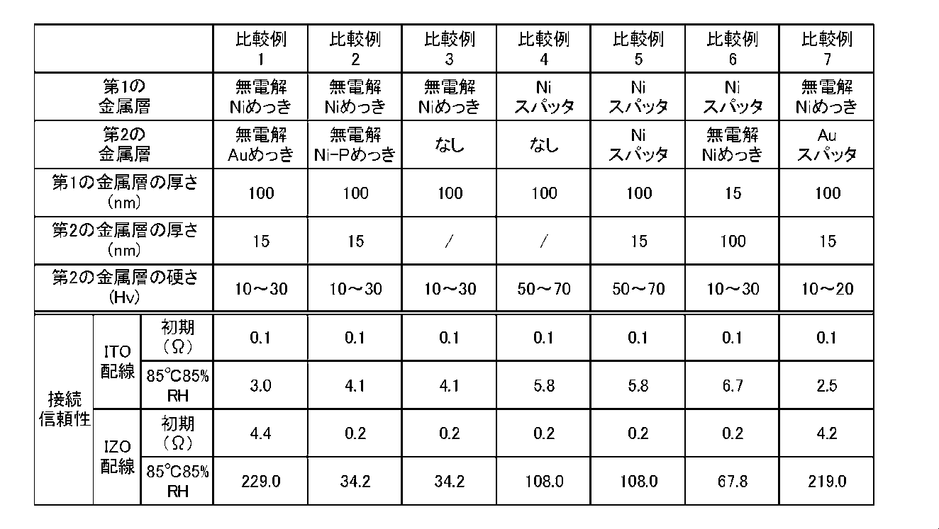
表1と表2とを比べれば分かるように、無電解金属めっき層を単独又は積層させても、IZO配線板に対して良好な接続信頼性が得られなかった(比較例1~3)。また、金属スパッタ層を単独又は積層させても、IZO配線板に対して良好な接続信頼性が得られなかった(比較例4、5)。また、第1の金属層を金属スパッタ層とし、第2の金属層を無電解金属めっき層とした場合も、IZO配線板に対して良好な接続信頼性が得られなかった(比較例6)。また、第1の金属層を無電解金属めっき層とし、第2の金属層をAuスパッタ層とした場合も、IZO配線板に対して良好な接続信頼性が得られなかった(比較例7)。
一方、実施例1~10に示すように、第1の金属層を無電解金属めっき層とし、第2の金属層をNiスパッタ層、Ruスパッタ層、Ru-Coスパッタ層、Wスパッタ層、Pdスパッタ層、Irスパッタ層、Coスパッタ層、Moスパッタ層のいずれかにすることにより、良好な接続信頼性が得られた。また、実施例1~10に示すように、第2の金属層のビッカース硬さ(Hv)が40以上の場合、良好な接続信頼性が得られ、特にビッカース硬さ(Hv)が300以上の場合、IZO配線板に対して良好な接続信頼性が得られた。また、実施例2~4に示すように、金属スパッタ層の厚さが5~30nmの場合、良好な接続信頼性が得られた。
11 樹脂粒子、12 無電解金属めっき層、13 金属スパッタ層
Claims (8)
- 樹脂粒子と、
前記樹脂粒子表面を被覆する無電解金属めっき層と、
最外層を形成するAuを除く金属スパッタ層と
を有する導電性粒子。 - 前記金属スパッタ層は、Ni、Ru、W、Pd、Ir、Co、Mo、Ti、Rh、Pt、又はこれらの1種以上を含む合金からなる請求項1記載の導電性粒子。
- 前記無電解金属めっき層は、無電解Niめっき層である請求項1又は2記載の導電性粒子。
- 前記金属スパッタ層のビッカース硬さ(Hv)が、40~500である請求項1乃至3のいずれか1項に記載の導電性粒子。
- 前記金属スパッタ層の厚さが、5~200nmである請求項1乃至4のいずれか1項に記載の導電性粒子。
- バインダ樹脂と、前記バインダ樹脂に分散された導電性粒子とを備え、
前記導電性粒子は、樹脂粒子と、前記樹脂粒子表面を被覆する無電解金属めっき層と、最外層を形成するAuを除く金属スパッタ層とを有する異方性導電材料。 - 樹脂粒子と、前記樹脂粒子表面を被覆する無電解金属めっき層と、最外層を形成するAuを除く金属スパッタ層とを有する導電性粒子によって第1の電子部品と第2の電子部品とが電気的に接続された接続構造体。
- 樹脂粒子と、前記樹脂粒子表面を被覆する無電解金属めっき層と、最外層を形成するAuを除く金属スパッタ層とを有する導電性粒子がバインダ樹脂に分散された異方性導電フィルムを第1の電子部品の端子上に貼付け、
前記異方性導電フィルム上に第2の電子部品を仮配置させ、
前記第2の電子部品上から加熱押圧装置により押圧し、
前記第1の電子部品の端子と、前記第2の電子部品の端子とを接続させる接続方法。
Priority Applications (2)
| Application Number | Priority Date | Filing Date | Title |
|---|---|---|---|
| KR1020137023157A KR20140045328A (ko) | 2011-02-04 | 2012-02-03 | 도전성 입자 및 이를 이용한 이방성 도전 재료 |
| CN2012800075384A CN103339687A (zh) | 2011-02-04 | 2012-02-03 | 导电性粒子及使用其的各向异性导电材料 |
Applications Claiming Priority (2)
| Application Number | Priority Date | Filing Date | Title |
|---|---|---|---|
| JP2011022451A JP2012164454A (ja) | 2011-02-04 | 2011-02-04 | 導電性粒子及びこれを用いた異方性導電材料 |
| JP2011-022451 | 2011-02-04 |
Publications (1)
| Publication Number | Publication Date |
|---|---|
| WO2012105701A1 true WO2012105701A1 (ja) | 2012-08-09 |
Family
ID=46602901
Family Applications (1)
| Application Number | Title | Priority Date | Filing Date |
|---|---|---|---|
| PCT/JP2012/052547 Ceased WO2012105701A1 (ja) | 2011-02-04 | 2012-02-03 | 導電性粒子及びこれを用いた異方性導電材料 |
Country Status (5)
| Country | Link |
|---|---|
| JP (1) | JP2012164454A (ja) |
| KR (1) | KR20140045328A (ja) |
| CN (1) | CN103339687A (ja) |
| TW (1) | TW201246235A (ja) |
| WO (1) | WO2012105701A1 (ja) |
Cited By (3)
| Publication number | Priority date | Publication date | Assignee | Title |
|---|---|---|---|---|
| CN104540777A (zh) * | 2013-07-19 | 2015-04-22 | Lg化学株式会社 | 用于形成透明导电膜的核-壳纳米颗粒及使用其的透明导电膜的制造方法 |
| JP2015210883A (ja) * | 2014-04-24 | 2015-11-24 | タツタ電線株式会社 | 金属被覆樹脂粒子及びそれを用いた導電性接着剤 |
| JP2016015312A (ja) * | 2014-06-11 | 2016-01-28 | 積水化学工業株式会社 | 導電性粒子、導電性粒子の製造方法、導電材料及び接続構造体 |
Families Citing this family (9)
| Publication number | Priority date | Publication date | Assignee | Title |
|---|---|---|---|---|
| KR101941721B1 (ko) * | 2011-12-21 | 2019-01-23 | 세키스이가가쿠 고교가부시키가이샤 | 도전성 입자, 도전 재료 및 접속 구조체 |
| KR101595182B1 (ko) * | 2014-06-11 | 2016-02-17 | 안우영 | 도전볼의 제조방법 |
| JP2016181511A (ja) * | 2015-03-23 | 2016-10-13 | デクセリアルズ株式会社 | 導電性粒子、異方性導電接着剤及び接続構造体 |
| CN108475583A (zh) * | 2016-02-18 | 2018-08-31 | 积水化学工业株式会社 | 电组件及电组件的制造方法 |
| JP7039883B2 (ja) | 2016-12-01 | 2022-03-23 | デクセリアルズ株式会社 | 異方性導電フィルム |
| KR102519781B1 (ko) | 2016-12-01 | 2023-04-10 | 데쿠세리아루즈 가부시키가이샤 | 이방성 도전 필름 |
| CN110494930B (zh) * | 2017-03-29 | 2021-10-01 | 昭和电工材料株式会社 | 导电粒子的分选方法、电路连接材料、连接结构体及其制造方法、以及导电粒子 |
| JP7292669B2 (ja) * | 2019-04-11 | 2023-06-19 | 株式会社レゾナック | 導電粒子の製造方法 |
| JP6794591B1 (ja) * | 2019-05-20 | 2020-12-02 | タツタ電線株式会社 | 導電性接着シート |
Citations (3)
| Publication number | Priority date | Publication date | Assignee | Title |
|---|---|---|---|---|
| JPH09143441A (ja) * | 1995-11-27 | 1997-06-03 | Three Bond Co Ltd | 異方導電性接着剤組成物 |
| JP2009032397A (ja) * | 2007-07-24 | 2009-02-12 | Sekisui Chem Co Ltd | 導電性微粒子 |
| JP2010080124A (ja) * | 2008-09-24 | 2010-04-08 | Sekisui Chem Co Ltd | 酸化亜鉛微粒子付着樹脂粒子及びその製造方法、並びに導電性粒子及びその製造方法 |
-
2011
- 2011-02-04 JP JP2011022451A patent/JP2012164454A/ja not_active Ceased
-
2012
- 2012-02-03 WO PCT/JP2012/052547 patent/WO2012105701A1/ja not_active Ceased
- 2012-02-03 CN CN2012800075384A patent/CN103339687A/zh active Pending
- 2012-02-03 KR KR1020137023157A patent/KR20140045328A/ko not_active Withdrawn
- 2012-02-04 TW TW101103661A patent/TW201246235A/zh unknown
Patent Citations (3)
| Publication number | Priority date | Publication date | Assignee | Title |
|---|---|---|---|---|
| JPH09143441A (ja) * | 1995-11-27 | 1997-06-03 | Three Bond Co Ltd | 異方導電性接着剤組成物 |
| JP2009032397A (ja) * | 2007-07-24 | 2009-02-12 | Sekisui Chem Co Ltd | 導電性微粒子 |
| JP2010080124A (ja) * | 2008-09-24 | 2010-04-08 | Sekisui Chem Co Ltd | 酸化亜鉛微粒子付着樹脂粒子及びその製造方法、並びに導電性粒子及びその製造方法 |
Cited By (3)
| Publication number | Priority date | Publication date | Assignee | Title |
|---|---|---|---|---|
| CN104540777A (zh) * | 2013-07-19 | 2015-04-22 | Lg化学株式会社 | 用于形成透明导电膜的核-壳纳米颗粒及使用其的透明导电膜的制造方法 |
| JP2015210883A (ja) * | 2014-04-24 | 2015-11-24 | タツタ電線株式会社 | 金属被覆樹脂粒子及びそれを用いた導電性接着剤 |
| JP2016015312A (ja) * | 2014-06-11 | 2016-01-28 | 積水化学工業株式会社 | 導電性粒子、導電性粒子の製造方法、導電材料及び接続構造体 |
Also Published As
| Publication number | Publication date |
|---|---|
| TW201246235A (en) | 2012-11-16 |
| CN103339687A (zh) | 2013-10-02 |
| JP2012164454A (ja) | 2012-08-30 |
| KR20140045328A (ko) | 2014-04-16 |
Similar Documents
| Publication | Publication Date | Title |
|---|---|---|
| JP2012164454A (ja) | 導電性粒子及びこれを用いた異方性導電材料 | |
| JP7506714B2 (ja) | 導電材料 | |
| JP6245792B2 (ja) | 導電性粒子、回路接続材料、実装体、及び実装体の製造方法 | |
| CN103493297B (zh) | 各向异性导电膜、连接方法和连接结构体 | |
| JP5114607B2 (ja) | 導電性粒子、導電性粒子の製造方法、異方性導電材料及び接続構造体 | |
| TW201140623A (en) | Anisotropic conductive material and connection structure | |
| TW201228835A (en) | Double layered anisotropic conductive film and apparatus comprising the same | |
| WO2011030715A1 (ja) | 絶縁粒子付き導電性粒子、絶縁粒子付き導電性粒子の製造方法、異方性導電材料及び接続構造体 | |
| JP4605225B2 (ja) | 回路接続材料、これを用いた回路部材の接続構造及びその製造方法 | |
| JP5608426B2 (ja) | 異方性導電膜の製造方法 | |
| TWI615072B (zh) | 各向異性導電薄膜、其連接方法及其接合體 | |
| JP6007022B2 (ja) | 回路接続材料 | |
| TW201807054A (zh) | 含導電性粒子之樹脂組成物及含該樹脂組成物之電子裝置 | |
| JP5580729B2 (ja) | 導電性粒子、異方性導電材料及び接続構造体 | |
| HK1189415A (en) | Electroconductive particles and anisotropic conductive material using same | |
| JP7312109B2 (ja) | 絶縁性粒子付き導電性粒子、絶縁性粒子付き導電性粒子の製造方法、導電材料及び接続構造体 | |
| JP7494411B1 (ja) | 導電性接着剤層 | |
| KR102749852B1 (ko) | 절연성 입자를 갖는 도전성 입자, 절연성 입자를 갖는 도전성 입자의 제조 방법, 도전 재료 및 접속 구조체 | |
| JP4682370B2 (ja) | 異方導電性シート | |
| WO2024116988A1 (ja) | 異方性導電フィルム、接続構造体および接続構造体の製造方法 | |
| KR102545861B1 (ko) | 도전 재료 |
Legal Events
| Date | Code | Title | Description |
|---|---|---|---|
| 121 | Ep: the epo has been informed by wipo that ep was designated in this application |
Ref document number: 12742551 Country of ref document: EP Kind code of ref document: A1 |
|
| DPE1 | Request for preliminary examination filed after expiration of 19th month from priority date (pct application filed from 20040101) | ||
| NENP | Non-entry into the national phase |
Ref country code: DE |
|
| ENP | Entry into the national phase |
Ref document number: 20137023157 Country of ref document: KR Kind code of ref document: A |
|
| 122 | Ep: pct application non-entry in european phase |
Ref document number: 12742551 Country of ref document: EP Kind code of ref document: A1 |