WO2012105124A1 - 電解コンデンサ及びその製造方法 - Google Patents
電解コンデンサ及びその製造方法 Download PDFInfo
- Publication number
- WO2012105124A1 WO2012105124A1 PCT/JP2011/078179 JP2011078179W WO2012105124A1 WO 2012105124 A1 WO2012105124 A1 WO 2012105124A1 JP 2011078179 W JP2011078179 W JP 2011078179W WO 2012105124 A1 WO2012105124 A1 WO 2012105124A1
- Authority
- WO
- WIPO (PCT)
- Prior art keywords
- foil
- cathode
- electrolytic capacitor
- fiber sheet
- anode
- Prior art date
- Legal status (The legal status is an assumption and is not a legal conclusion. Google has not performed a legal analysis and makes no representation as to the accuracy of the status listed.)
- Ceased
Links
Images



Classifications
-
- H—ELECTRICITY
- H01—ELECTRIC ELEMENTS
- H01G—CAPACITORS; CAPACITORS, RECTIFIERS, DETECTORS, SWITCHING DEVICES, LIGHT-SENSITIVE OR TEMPERATURE-SENSITIVE DEVICES OF THE ELECTROLYTIC TYPE
- H01G9/00—Electrolytic capacitors, rectifiers, detectors, switching devices, light-sensitive or temperature-sensitive devices; Processes of their manufacture
- H01G9/004—Details
- H01G9/02—Diaphragms; Separators
-
- H—ELECTRICITY
- H01—ELECTRIC ELEMENTS
- H01G—CAPACITORS; CAPACITORS, RECTIFIERS, DETECTORS, SWITCHING DEVICES, LIGHT-SENSITIVE OR TEMPERATURE-SENSITIVE DEVICES OF THE ELECTROLYTIC TYPE
- H01G9/00—Electrolytic capacitors, rectifiers, detectors, switching devices, light-sensitive or temperature-sensitive devices; Processes of their manufacture
- H01G9/004—Details
- H01G9/008—Terminals
-
- H—ELECTRICITY
- H01—ELECTRIC ELEMENTS
- H01G—CAPACITORS; CAPACITORS, RECTIFIERS, DETECTORS, SWITCHING DEVICES, LIGHT-SENSITIVE OR TEMPERATURE-SENSITIVE DEVICES OF THE ELECTROLYTIC TYPE
- H01G9/00—Electrolytic capacitors, rectifiers, detectors, switching devices, light-sensitive or temperature-sensitive devices; Processes of their manufacture
- H01G9/004—Details
- H01G9/04—Electrodes or formation of dielectric layers thereon
- H01G9/048—Electrodes or formation of dielectric layers thereon characterised by their structure
-
- H—ELECTRICITY
- H01—ELECTRIC ELEMENTS
- H01G—CAPACITORS; CAPACITORS, RECTIFIERS, DETECTORS, SWITCHING DEVICES, LIGHT-SENSITIVE OR TEMPERATURE-SENSITIVE DEVICES OF THE ELECTROLYTIC TYPE
- H01G9/00—Electrolytic capacitors, rectifiers, detectors, switching devices, light-sensitive or temperature-sensitive devices; Processes of their manufacture
- H01G9/004—Details
- H01G9/08—Housing; Encapsulation
- H01G9/10—Sealing, e.g. of lead-in wires
Definitions
- the present invention relates to a wound electrolytic capacitor and a method for manufacturing the same.
- FIG. 12 is a cross-sectional view showing a conventional solid electrolytic capacitor among various electrolytic capacitors.
- the solid electrolytic capacitor includes a winding element 80, a bottomed cylindrical outer case 85 that accommodates the winding element 80, and a rubber that seals an opening 850 of the outer case 85. And a sealing member 86 made of metal.
- the winding element 80 has a wound body 81, an anode lead tab terminal 83, and a cathode lead tab terminal 84.
- Lead portions 830 and 840 are respectively formed on the anode lead tab terminal 83 and the cathode lead tab terminal 84, and the lead portions 830 and 840 are drawn out of the exterior case 85 through the sealing member 86. .
- FIG. 13 is a perspective view showing a wound body 81 of the conventional solid electrolytic capacitor.
- the wound body 81 is configured by overlapping and winding an anode foil 811 and a cathode foil 812, and the anode lead tab terminal 83 is electrically connected to the anode foil 811.
- a cathode lead tab terminal 84 is electrically connected to the cathode foil 812 (see, for example, Patent Document 1).
- a dielectric coating is formed on the surface of the anode foil 811 by subjecting the surface to chemical conversion treatment.
- paper separators 813 are stacked on the anode foil 811 and the cathode foil 812, respectively. By impregnating and polymerizing the separator 813 with a chemical polymerization solution, the anode foil 811 and A solid electrolyte layer is formed between the cathode foil 812 and the cathode foil 812.
- Various electrolytic capacitors including the above-described solid electrolytic capacitor can function as a noise filter that removes high-frequency noise generated from a processing device such as a CPU (Central Processing Unit).
- a processing device such as a CPU (Central Processing Unit).
- electrolytic capacitors having a large capacity are demanded despite their small size.
- the processing speed of a processing unit such as a CPU is increased, and therefore, the amount of current supplied to the processing unit increases, and the noise band tends to shift to the high frequency side. Therefore, the electrolytic capacitor is required to have a low ESR (equivalent series resistance).
- the following methods can be considered to realize large capacity. For example, by etching the surface of the anode foil 811 to form fine irregularities, the surface area of the anode foil 811 is increased.
- the voltage applied to the anode foil 811 is reduced to reduce the thickness of the dielectric coating formed on the surface of the anode foil 811.
- the capacitance of the electrolytic capacitor is increased as compared with the conventional one, while the leakage current is likely to increase, thereby causing a short circuit failure.
- the capacity of the electrolytic capacitor can be increased. However, this increases the size of the electrolytic capacitor.
- the thickness of the cathode foil 812 and the separator 813 are reduced in order to realize both the increase in capacity and miniaturization of the solid electrolytic capacitor, and the reduced thickness is used as the anode. It is considered to replace the foil 811 and increase the winding amount of the anode foil 811.
- the strengths of the cathode foil 812 and the separator 813 are reduced by the reduction in thickness.
- the anode foil 811, the cathode foil 812, and the two separators 813, 813 are respectively tensioned when the wound body 81 is manufactured in the manufacturing process. It is wound.
- the cathode foil 812 and the separator 813 cannot withstand the tension during winding and may break. Therefore, it is difficult to increase the capacity and size of the solid electrolytic capacitor.
- an object of the present invention is to realize a large capacity and a small size in a wound electrolytic capacitor.
- the electrolytic capacitor according to the present invention includes a wound body configured by winding an electrode foil.
- the fiber sheet is integrated with the electrode foil by fixing an electrically insulating fiber sheet to both surfaces thereof.
- the fiber sheet is bonded and fixed to both surfaces of the electrode foil.
- the fiber layer used as the said fiber sheet may be formed by fixing a fiber to both surfaces of this electrode foil.
- the wound body is configured by overlapping and winding a plurality of the electrode foils, and the fiber sheet includes a plurality of electrodes constituting the wound body.
- the foil is fixed to both surfaces of at least one electrode foil.
- the plurality of electrode foils include an anode foil and a cathode foil having a dielectric film formed on a surface thereof, and the anode foil and the cathode foil are overlapped with each other.
- the wound body is configured by winding.
- the fiber sheet is fixed to both surfaces of the cathode foil.
- the electrolytic capacitor further includes a lead tab terminal, and the lead tab terminal is disposed on the fiber sheet and electrically connected to an electrode foil in which the fiber sheet is integrated. Connected.
- the method for producing an electrolytic capacitor according to the present invention includes a step of preparing an electrode foil, and the fiber sheet is integrated by fixing an electrically insulating fiber sheet to at least one surface of the electrode foil. By arranging a lead tab terminal on the fiber sheet integrated with the electrode foil, electrically connecting the electrode foil and the lead tab terminal to each other, and winding the electrode foil, And a step of producing a wound body.
- the electrolytic capacitor of the present invention its capacity and size can be reduced.
- an electrolytic capacitor having a large capacity and a small size can be manufactured.
- FIG. 3 is a sectional view taken along line AA shown in FIG. 2. It is a top view used for description of an integration process among the manufacturing methods of the said solid electrolytic capacitor.
- FIG. 5 is a sectional view taken along line BB shown in FIG. 4. It is a top view used for description of the 1st terminal attachment process among this manufacturing method. It is a top view used for description of the 2nd terminal attachment process among this manufacturing method. It is a perspective view used for description of the front
- FIG. 1 is a perspective view showing a solid electrolytic capacitor according to an embodiment of the present invention
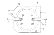
- FIG. 2 is a bottom view of the solid electrolytic capacitor
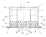
- FIG. 3 is a cross-sectional view taken along the line AA shown in FIG.
- the solid electrolytic capacitor includes a capacitor body 1, a seat plate 2 on which the capacitor body 1 is mounted, an anode terminal 3, and a cathode terminal 4.
- both the anode terminal 3 and the cathode terminal 4 are exposed on the lower surface 2 b of the seat plate 2.
- the lower surface 2 b of the seat plate 2 includes a first groove portion 201 that extends to the edge 21 of the seat plate 2 and a second groove portion 202 that extends to the edge 22 opposite to the edge 21. It is recessed.
- the first groove 201 accommodates the anode terminal 3, while the second groove 202 accommodates the cathode terminal 4.
- the capacitor body 1 includes a winding element 10, a bottomed cylindrical outer case 5 in which the winding element 10 is accommodated, and an opening 50 of the outer case 5.
- a rubber sealing member 6 is made of a metal material such as aluminum, and the sealing member 6 is fixed to the outer case 5 by subjecting the opening end of the outer case 5 to horizontal drawing and curling. Yes.
- the exterior case 5 is not limited to a metal material, and may be formed from various materials including an electrical insulating material.
- the opening 50 of the outer case 5 may be sealed by pouring a resin material into the outer case 5 and solidifying the resin material.
- the winding element 10 has a wound body 11 as shown in FIG.
- FIG. 9 is a perspective view used for explaining the latter stage of the winding process in the manufacturing method described later.
- the wound body 11 is configured by winding an anode foil 111 and a cathode foil 112 so as to overlap each other.
- the anode foil 111 and the cathode foil 112 are each formed from a valve metal such as aluminum, tantalum, or niobium.
- the anode foil 111 has a dielectric film formed on the surface thereof.
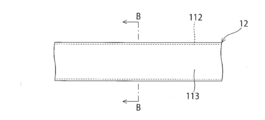
- an electrically insulating fiber sheet 113 is integrated with the cathode foil 112, and the fiber sheet 113 and the cathode foil 112 constitute one cathode composite sheet 12.
- FIG. 4 is a plan view used for explaining the integration step in the manufacturing method described later
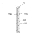
- FIG. 5 is a cross-sectional view taken along the line BB shown in FIG.
- the cathode foil 112 and the fiber sheet 113 are integrated by sticking and fixing the fiber sheet 113 to both surfaces 112a and 112b of the cathode foil 112.
- An adhesive member such as an adhesive or a double-sided tape is used for adhering the fiber sheet 113 to the cathode foil 112.
- a woven fabric or a non-woven fabric formed from a fiber material such as cellulose, aramid, polyester, nylon, and vinylon is used.
- a fiber layer that becomes the fiber sheet 113 is formed on both surfaces 112a and 112b of the cathode foil 112 by fixing a fiber material to the both surfaces 112a and 112b instead of adhering and fixing the fiber sheet 113.
- materials such as cellulose, aramid, polyester, nylon, and vinylon can be used as the fiber material.
- the fiber material can be fixed to both surfaces 112a and 112b of the cathode foil 112 by spraying the fiber material onto the both surfaces 112a and 112b.
- a solid electrolyte layer is formed on the wound body 11.
- the solid electrolyte layer is formed inside the wound body 11. That is, the wound body 11 is impregnated with an electrolyte that becomes a solid electrolyte layer.
- the fiber sheet 113 is impregnated with a precursor for forming a solid electrolyte layer, for example, a polymerized liquid containing a conductive polymer, so that a gap (mainly in the wound body 11 (mainly The solid electrolyte layer is formed in a state in which a gap formed between the anode foil 111 and the cathode foil 112 is filled.
- the solid electrolyte layer may also be formed outside the wound body 11, that is, on the outer peripheral surface of the wound body 11.
- the winding element 10 further has an anode lead tab terminal 30 and a cathode lead tab terminal 40 as shown in FIG. 8 (see also FIG. 3).
- FIG. 8 is a perspective view used for explanation of the former stage of the winding process in the manufacturing method described later.
- the anode lead tab terminal 30 is attached to the anode foil 111.
- the cathode lead tab terminal 40 is attached to the cathode composite sheet 12. As shown in FIG. 9, the anode lead tab terminal 30 and the cathode lead tab terminal 40 are drawn from the same winding end surface 11 a of the winding body 11.
- the anode lead tab terminal 30 has a lead portion 31 and a flat portion 32, and the flat portion 32 is attached to the anode foil 111.
- the lead portion 31 of the anode lead tab terminal 30 is drawn from the winding end surface 11 a of the winding body 11.
- the anode lead tab terminal 30 is attached to the anode foil 111 by crimping the flat portion 32 to the anode foil 111. Therefore, the anode lead tab terminal 30 is electrically connected to the anode foil 111.
- a method for crimping the anode lead tab terminal 30 to the anode foil 111 will be described in a first terminal attaching step (FIGS. 6A and 6B) of a manufacturing method described later.
- the cathode lead tab terminal 40 has a lead portion 41 and a flat portion 42, and the flat portion 42 is attached to the cathode composite sheet 12.
- the lead portion 41 of the cathode lead tab terminal 40 is drawn from the winding end surface 11 a of the winding body 11.
- the cathode lead tab terminal 40 is arranged on the cathode composite sheet 12 by arranging the flat portion 42 on the fiber sheet 113 of the cathode composite sheet 12 and crimping the flat portion 42 to the cathode composite sheet 12. It is attached. Therefore, the cathode lead tab terminal 40 is electrically connected to the cathode foil 112 constituting the cathode composite sheet 12.
- the method of crimping the cathode lead tab terminal 40 to the cathode composite sheet 12 will be described in a second terminal attaching step (FIGS. 7A and 7B) of the manufacturing method described later.
- the anode lead tab terminal 30 is provided at a position different from the winding shaft 110, while the cathode lead tab terminal 40 is connected to the anode lead tab terminal 30 with respect to the winding shaft 110. Is provided at the opposite position. Then, the lead portions 31 and 41 of the anode lead tab terminal 30 and the cathode lead tab terminal 40 pass through the sealing member 6 and are drawn to the outside of the outer case 5.
- the winding shaft 110 of the wound body 11 substantially coincides with the center position 52 of the opening 50 of the outer case 5. Accordingly, the lead portion 31 of the anode lead tab terminal 30 is drawn out of the exterior case 5 from a position different from the center position 52 of the opening 50 of the exterior case 5, while the lead portion 41 of the cathode lead tab terminal 40 is extracted from the exterior case 5. From the position opposite to the lead position of the lead portion 31 of the anode lead tab terminal 30 with respect to the center position 52 of the opening 50, the lead is pulled out of the outer case 5.
- the seat plate 2 is formed with two through holes 20, 20 that penetrate the seat plate 2 from the upper surface 2 a to the lower surface 2 b, and the two through holes 20, 20 communicates with a first groove 201 and a second groove 202 provided on the lower surface 2b of the seat plate 2, respectively.
- the lead portion 31 of the anode lead tab terminal 30 passes through the corresponding through hole 20 of the seat plate 2 and then bends in the vicinity of the outlet of the through hole 20, and then the first lead along the first groove portion 201.
- the groove 201 extends to the edge 21 of the seat plate 2.
- a portion of the lead portion 31 extending in the first groove portion 201 along the first groove portion 201 has a flat shape, and the flat portion constitutes the anode terminal 3 of the solid electrolytic capacitor. Yes.
- the lead portion 41 of the cathode lead tab terminal 40 passes through the corresponding through hole 20 of the seat plate 2, then bends in the vicinity of the outlet of the through hole 20, and then the second portion along the second groove portion 202.
- the groove 202 extends to the edge 22 of the seat plate 2.
- a portion of the lead 41 that extends in the second groove 202 along the second groove 202 has a flat shape, and the flat portion constitutes the cathode terminal 4 of the solid electrolytic capacitor. Yes.
- a foil preparation process an integration process, a first terminal attachment process, a second terminal attachment process, a winding process, a re-chemical conversion treatment process, an electrolyte layer formation process, and an assembly process are sequentially executed.
- a metal foil to be the anode foil 111 is prepared. Then, the surface of the metal foil is etched to form a plurality of fine irregularities, thereby increasing the surface area of the metal foil. Next, a chemical film is applied to the surface of the metal foil to form a dielectric film on the surface. Thereafter, the metal foil is cut to cut the metal foil into a long predetermined shape. Thereby, the anode foil 111 having a dielectric film formed on the surface is produced. In addition, in the produced anode foil 111, a part of metal which comprises this anode foil 111 will be exposed to the cut surface (end surface).
- a metal foil to be the cathode foil 112 is further prepared. Then, the metal foil is cut to cut the metal foil into a long predetermined shape. Thereby, the cathode foil 112 is produced.
- the fiber sheet 113 is stuck and fixed to both surfaces 112 a and 112 b of the cathode foil 112. Thereby, the fiber sheet 113 is integrated with the cathode foil 112, and as a result, one cathode composite sheet 12 composed of the fiber sheet 113 and the cathode foil 112 is produced (see also FIG. 4).
- the fiber material may be fixed to both surfaces 112a and 112b of the cathode foil 112 instead of sticking and fixing the fiber sheet 113 to both surfaces 112a and 112b of the cathode foil 112. Thereby, the fiber layer used as the fiber sheet 113 is formed in this both surfaces 112a and 112b.
- the integration process may be performed on the metal foil to be the cathode foil 112. That is, the fiber sheet 113 may be stuck and fixed to both surfaces of the metal foil, and then the metal foil may be cut into a long predetermined shape. Also in this case, the cathode foil 112 (cathode composite sheet 12) in which the fiber sheet 113 is integrated is produced.
- FIGS. 6A and 6B are plan views used for explaining the first terminal mounting step.
- the first terminal attaching step is a step of attaching the anode lead tab terminal 30 to the anode foil 111.
- FIG. 6A is a plan view of the anode foil 111 viewed from the anode lead tab terminal 30 side.
- FIG. 6B is a plan view of the anode foil 111 as viewed from the side opposite to the anode lead tab terminal 30.
- the flat portion 32 of the anode lead tab terminal 30 is crimped to the anode foil 111, whereby the anode foil 111 has an anode.
- the lead tab terminal 30 is attached.
- a crimping needle (not shown) is inserted into the flat portion 32 of the anode lead tab terminal 30 and the anode foil 111 from the anode lead tab terminal 30 side.
- the tip of the crimping needle has a quadrangular pyramid shape.
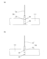
- the flat portion 32 of the anode lead tab terminal 30 is formed with a through hole 34 as shown in FIG. 6 (a) by the piercing of the crimping needle, and further, the flat portion 32 has a through hole shown in FIG. 6 (b).
- a petal-like burr 33 is formed in a state of penetrating the anode foil 111. At this time, burrs are also formed on the anode foil 111.
- the burrs 33 are crushed on the surface of the anode foil 111.
- the flat portion 32 of the anode lead tab terminal 30 is crimped to the anode foil 111.
- the anode lead tab terminal 30 is electrically connected to the anode foil 111 by crimping the anode lead tab terminal 30 to the anode foil 111.
- the dielectric coating may be damaged by caulking the anode lead tab terminal 30 to the anode foil 111.
- FIGS. 7A and 7B are plan views used for explaining the second terminal mounting step.
- the second terminal attaching step is a step of attaching the cathode lead tab terminal 40 to the cathode composite sheet 12.
- FIG. 7A is a plan view of the cathode composite sheet 12 viewed from the cathode lead tab terminal 40 side.
- FIG. 7B is a plan view of the cathode composite sheet 12 viewed from the side opposite to the cathode lead tab terminal 40.
- the flat portion 42 of the cathode lead tab terminal 40 is disposed on the fiber sheet 113 of the cathode composite sheet 12, and the flat portion. 42 is crimped to the cathode composite sheet 12, whereby the cathode lead tab terminal 40 is attached to the cathode composite sheet 12.
- a caulking needle (not shown) is inserted into the flat portion 42 of the cathode lead tab terminal 40 and the cathode composite sheet 12 from the cathode lead tab terminal 40 side.
- the tip of the crimping needle has a quadrangular pyramid shape.
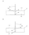
- the flat portion 42 of the cathode lead tab terminal 40 is formed with a through hole 44 as shown in FIG. 7 (a) by the piercing of the crimping needle, and further, the flat portion 42 has a through hole 44 as shown in FIG. 7 (b).
- the petal-like burrs 43 are formed in a state of penetrating the cathode composite sheet 12.
- burrs are also formed on the cathode foil 112 constituting the cathode composite sheet 12.
- the burrs 43 are crushed on the surface of the cathode composite sheet 12.
- the flat portion 42 of the cathode lead tab terminal 40 is crimped to the cathode composite sheet 12.
- the cathode lead tab terminal 40 is electrically connected to the cathode foil 112 constituting the cathode composite sheet 12 by caulking the cathode lead tab terminal 40 to the cathode composite sheet 12.
- the anode foil 111 and the cathode composite sheet 12 are overlapped with each other and wound, whereby the wound body 11 is produced.
- the anode lead tab terminal 30 and the cathode lead tab terminal 40 protrude from the same winding end surface 11 a of the wound body 11, and further, the cathode lead tab terminal 40 is wound around the winding shaft 110 in the wound body 11.
- the anode foil 111 and the cathode composite sheet 12 are overlapped and wound so as to be disposed at a position opposite to the anode lead tab terminal 30.
- the terminal portion of the cathode composite sheet 12 is fixed to the outer peripheral surface of the wound body 11 by a winding tape 114 as shown in FIG.
- the terminal portion of the anode foil 111 is fixed to the outer peripheral surface of the wound body 11 by the winding tape 114.
- the winding tape 114 a conductive tape can be used. In the winding process, stress is generated in the dielectric film due to the winding of the anode foil 111, which may damage the dielectric film.
- the wound body 11 is immersed in the chemical conversion solution, and a voltage is applied to the anode foil 111 through the anode lead tab terminal 30 in this state.
- an aqueous solution of ammonium adipate is used as the chemical conversion solution.
- a re-forming process is performed on the wound body 11, and as a result, an oxide film (dielectric film) is formed on the cut surface (end surface) of the anode foil 111, and the damaged part of the dielectric film Is repaired.
- the entire surface of the anode foil 111 is covered with the dielectric film.
- a precursor for forming a solid electrolyte layer for example, a polymerization solution containing a conductive polymer is prepared, and the wound body 11 is immersed in the polymerization solution.
- the fiber sheet 113 constituting the cathode composite sheet 12 is impregnated with the polymerization liquid and polymerized, whereby the gaps (mainly, the anode foil 111 and the cathode composite sheet 12 existing in the wound body 11).
- the conductive polymer film is formed in a state where the gap is filled in the gap formed between the cathode foil 112 and the cathode foil 112.
- a conductive polymer film is also formed on the outer peripheral surface of the wound body 11. Thereby, a solid electrolyte layer is comprised by these electroconductive polymer films, and the winding element 10 is completed.
- the winding element 10 is fixed to the sealing member 6 (see FIG. 3). Specifically, the lead part 31 of the anode lead tab terminal 30 and the lead part 41 of the cathode lead tab terminal 40 are penetrated through the sealing member 6. Thereafter, the winding element 10 is accommodated in the outer case 5 and the opening 50 of the outer case 5 is closed by the sealing member 6. Then, the sealing member 6 is fixed to the outer case 5 by performing lateral drawing and curling on the opening end of the outer case 5, thereby sealing the opening 50 of the outer case 5. As a result, the winding element 10 is fixed in the outer case 5 to complete the capacitor body 1 (see FIG. 1).
- the capacitor body 1 is further mounted on the seat plate 2 (see FIGS. 1 to 3).
- the lead portion 31 of the anode lead tab terminal 30 is inserted into the through hole 20 that communicates with the first groove portion 201.
- the lead portion 41 of the cathode lead tab terminal 40 is inserted into the through hole 20 that communicates with the second groove portion 202.
- the lead portions 31 and 41 are each subjected to press processing on the portions protruding from the lower surface 2b of the seat plate 2, thereby deforming the portions into flat shapes.
- the flat portion of the lead portion 31 is accommodated in the first groove portion 201 by bending the lead portion 31 of the anode lead tab terminal 30 in the vicinity of the outlet of the through hole 20.
- the lead portion 41 of the cathode lead tab terminal 40 is accommodated in the second groove portion 202.
- the flat portions of the lead portions 31 and 41 constitute the anode terminal 3 and the cathode terminal 4 exposed on the lower surface 2b of the seat plate 2, respectively.
- the fiber sheet 113 is integrated with the cathode foil 112. For this reason, when producing the wound body 11 as shown in FIG. 8, it is not necessary to apply tension to each of the cathode foil 112 and the fiber sheet 113, and the cathode foil 112 and the fiber sheet 113 are integrated. What is necessary is just to apply tension with respect to the one cathode composite sheet 12 comprised. Therefore, the thickness dimension of the cathode composite sheet 12 (total thickness dimension of the cathode foil 112 and the fiber sheet 113) until the strength of the cathode composite sheet 12 reaches a lower limit value that can withstand the tension during winding. Can be reduced.
- the solid electrolytic capacitor even when the thickness dimensions of the cathode foil 112 and the fiber sheet 113 are smaller than the thickness dimensions of the cathode foil 812 and the separator 813 of the conventional solid electrolytic capacitor (see FIG. 13), respectively.
- the wound body 11 can be produced without breaking the cathode foil 112 and the fiber sheet 113. Therefore, the anode foil 111 is replaced by replacing the reduced thickness of the cathode foil 112 and the fiber sheet 113 with the anode foil 111, thereby increasing the capacity and size of the solid electrolytic capacitor. Will be.
- the anode foil 111 and the cathode composite sheet 12 may be wound in the process of manufacturing the wound body 11, and at this time, a fiber sheet such as a separator is newly prepared and wound. There is no need to turn. Therefore, the wound body 11 can be easily manufactured.
- the inventor of the present application conducted an experiment for measuring the capacitance and ESR of the solid electrolytic capacitor according to the present embodiment (see FIGS. 3 and 8) and the conventional solid electrolytic capacitor (see FIGS. 12 and 13). It was.
- the fiber sheet 113 is integrated with the cathode foil 112
- the separator 813 is integrated with the cathode foil 812.
- the entire thickness dimension of the cathode foil 112 and the fiber sheet 113 of the solid electrolytic capacitor according to the present embodiment is smaller than the entire thickness dimension of the cathode foil 812 and the separator 813 of the conventional solid electrolytic capacitor.
- the outer dimensions of the solid electrolytic capacitor were made the same between this embodiment and the conventional one. Further, the measurement frequency of capacitance was 120 Hz, and the measurement frequency of ESR was 100 kHz.
- the capacitance was 336 ⁇ F and the ESR was 12 m ⁇ , whereas in the solid electrolytic capacitor according to this embodiment, the capacitance was 653 ⁇ F and the ESR was 13 m ⁇ . . From this result, it was confirmed that large capacity was realized in the solid electrolytic capacitor according to the present embodiment. Further, it was confirmed that the ESR of the solid electrolytic capacitor according to the present embodiment and the conventional solid electrolytic capacitor are approximately the same.
- the inventor of the present application integrates the cathode foil 112 and the fiber sheet 113 to form the cathode composite sheet 12, so that the thickness dimension of the cathode composite sheet 12 is set to the cathode foil used in the conventional solid electrolytic capacitor. Alternatively, it is considered that the thickness can be made equal to or smaller than the individual thickness dimension of the separator.
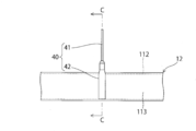
- FIG. 10 is a plan view showing a mounting structure of the cathode lead tab terminal 40 in a modified example of the solid electrolytic capacitor.
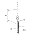
- FIG. 11 is a sectional view taken along the line CC shown in FIG.
- the cathode lead tab terminal 40 may be attached to the cathode composite sheet 12 by sticking and fixing the flat portion 42 to the cathode composite sheet 12.
- the cathode lead tab terminal 40 is electrically connected to the cathode foil 112 through a solid electrolyte layer formed by impregnating the fiber sheet 113 constituting the cathode composite sheet 12 with the polymerization liquid. Become.
- an adhesive member 70 such as an adhesive or a double-sided tape is used to attach the cathode lead tab terminal 40 to the cathode composite sheet 12.
- the adhesive member 70 may be conductive or electrically insulating.
- electrical connection between the solid electrolyte layer formed by impregnating the polymer sheet into the fiber sheet 113 constituting the cathode composite sheet 12 and the cathode lead tab terminal 40 is performed. This increases the connection area, which reduces the ESR of the solid electrolytic capacitor.
- the solid electrolytic capacitor may have a configuration in which the fiber sheet 113 is fixed only to one side 112a (or 112b) of the cathode foil 112.
- the fiber sheet 113 is fixed only to one side 112a (or 112b) of the cathode foil 112 in the integration step.
- the solid electrolytic capacitor having such a configuration even in the step of producing a wound body, it is necessary to prepare and wind a fiber sheet such as a separator separately from the anode foil 111 and the cathode composite sheet 12.
- the number is less than that of a conventional solid electrolytic capacitor. Therefore, it is easy to produce a wound body.
- each of the anode foil 111 and the cathode foil 112 constituting the wound body 11 is not limited to one, and may be a plurality of two or more.
- the number of anode lead tab terminals 30 and cathode lead tab terminals 40 is not limited to one, and may be two or more.
- the fiber sheet 113 may be integrated with the anode foil 111 by being fixed to both surfaces or one surface of the anode foil 111.
- the wound body 11 is formed by winding at least one anode foil 111 without overlapping the cathode foil 112 on the anode foil 111.
- the sheet 113 may be fixed. That is, in the solid electrolytic capacitor, the wound body 11 is configured by winding at least one electrode foil (anode foil 111 or cathode foil 112), and among the electrode foils constituting the wound body 11
- the fiber sheet 113 may be integrated with the electrode foil by fixing the fiber sheet 113 to both surfaces or one surface of at least one electrode foil.
- the integrated structure of the fiber sheet 113 employed in the solid electrolytic capacitor can be applied not only to the solid electrolytic capacitor but also to an electrolytic solution type electrolytic capacitor.
- Winding body 111 Anode foil 112 Cathode foil 113 Fiber sheet 12 Cathode composite sheet 30 Anode lead tab terminal 40 Cathode lead tab terminal
Landscapes
- Engineering & Computer Science (AREA)
- Power Engineering (AREA)
- Microelectronics & Electronic Packaging (AREA)
- Fixed Capacitors And Capacitor Manufacturing Machines (AREA)
Abstract
【課題】巻回型の電解コンデンサにおいて、その大容量化と小型化とを実現する。 【解決手段】本発明に係る電解コンデンサは、電極箔111,112を巻回することにより構成された巻回体11を備えている。ここで、電極箔112には、その両面に電気絶縁性の繊維シート113を固着させることにより該繊維シート113が一体化されている。具体的には、繊維シート113が一体化されている電極箔112において、繊維シート113は、電極箔112の両面に貼着固定されている。電極箔112の両面には、該両面に繊維を固着させることにより、繊維シート113となる繊維層が形成されていてもよい。
Description
本発明は、巻回型の電解コンデンサ及びその製造方法に関する。
図12は、種々の電解コンデンサの内、従来の固体電解コンデンサを示した断面図である。図12に示す様に、該固体電解コンデンサは、巻回素子80と、該巻回素子80が収容される有底筒状の外装ケース85と、該外装ケース85の開口850を封止するゴム製の封口部材86とを備えている。ここで、巻回素子80は、巻回体81と、陽極リードタブ端子83と、陰極リードタブ端子84とを有している。そして、陽極リードタブ端子83及び陰極リードタブ端子84にはそれぞれリード部830,840が形成されており、該リード部830,840が、封口部材86を貫通して外装ケース85の外部へ引き出されている。
図13は、上記従来の固体電解コンデンサの巻回体81を示した斜視図である。図13に示す様に、巻回体81は、陽極箔811と陰極箔812とを重ね合わせて巻回することにより構成されており、陽極箔811に陽極リードタブ端子83が電気的に接続される一方、陰極箔812に陰極リードタブ端子84が電気的に接続されている(例えば、特許文献1参照)。ここで、陽極箔811の表面には、該表面に化成処理を施すことによって誘電体被膜が形成されている。又、図13に示す様に、陽極箔811及び陰極箔812にはそれぞれ紙製のセパレータ813が重ねられており、該セパレータ813に化学重合液を含浸させて重合させることにより、陽極箔811と陰極箔812との間に固体電解質層が形成されている。
上記固体電解コンデンサを含む種々の電解コンデンサは、CPU(Central Processing Unit)等の処理装置から生じる高周波ノイズを除去するノイズフィルタとして機能させることが出来る。
近年、電子機器の小型化に伴い、電解コンデンサにおいて、それが小型であるにも拘わらず大容量であるものが求められている。又、CPU等の処理装置は、その動作速度が高速化しており、このため、処理装置に供給される電流量が増大し、又、ノイズの帯域が高周波側へシフトする傾向にある。従って、電解コンデンサにおいて、その低ESR(等価直列抵抗)化が求められている。
大容量化の実現には、次の様な手法が考えられる。例えば、陽極箔811の表面にエッチングを施して微細な凹凸を形成することにより、陽極箔811の表面積を増大させる。或いは、陽極箔811の表面に化成処理を施す際、陽極箔811に印加する電圧を小さくすることにより、陽極箔811の表面に形成される誘電体被膜の厚さ寸法を小さくする。しかしながら、これらの手法によれば、電解コンデンサの静電容量が従来のものに比べて増加する一方で、漏れ電流が増大し易くなり、延いてはショート不良が発生することになる。
又、陽極箔811と陰極箔812の巻回量を増やしてこれらの対向面積を増大させることにより、電解コンデンサの大容量化を実現することが出来る。しかしながら、これでは電解コンデンサが大型化することになる。
例えば固体電解コンデンサにおいて、該固体電解コンデンサの大容量化と小型化の両方を実現するべく、陰極箔812とセパレータ813の厚さ寸法をそれぞれ小さくし、該厚さ寸法が小さくなった分を陽極箔811に置き換えて陽極箔811の巻回量を増やすことが考えられている。しかしながら、厚さ寸法が小さくなった分、陰極箔812とセパレータ813の強度がそれぞれ低下することになる。ここで、従来の固体電解コンデンサにおいては、その製造過程にて巻回体81を作製する際、陽極箔811、陰極箔812、及び2枚のセパレータ813,813が、各々にテンションが掛けられながら巻回される。このため、従来の固体電解コンデンサにおいて単に陰極箔812とセパレータ813の厚さ寸法をそれぞれ小さくしたのでは、陰極箔812やセパレータ813が、巻回時のテンションに耐えることが出来ずに破断する虞があり、従って、固体電解コンデンサの大容量化と小型化の実現が難しい。
そこで本発明の目的は、巻回型の電解コンデンサにおいて、その大容量化と小型化とを実現することである。
本発明に係る電解コンデンサは、電極箔を巻回することにより構成された巻回体を備えている。ここで、前記電極箔には、その両面に電気絶縁性の繊維シートを固着させることにより該繊維シートが一体化されている。具体的には、前記繊維シートが一体化されている電極箔において、前記繊維シートは、電極箔の両面に貼着固定されている。尚、前記繊維シートが一体化されている電極箔において、該電極箔の両面に繊維を固着させることにより、前記繊維シートとなる繊維層が形成されていてもよい。
上記電解コンデンサの具体的構成において、前記巻回体は、前記電極箔を複数枚重ね合わせて巻回することにより構成されたものであり、前記繊維シートは、巻回体を構成する複数の電極箔の内、少なくとも1つの電極箔の両面に固着されている。
上記電解コンデンサの他の具体的構成において、前記複数の電極箔には、表面に誘電体被膜が形成された陽極箔と、陰極箔とが含まれ、該陽極箔と陰極箔とを互いに重ね合わせて巻回することにより前記巻回体が構成されている。そして、前記繊維シートは、前記陰極箔の両面に固着されている。
上記電解コンデンサの更なる他の具体的構成において、電解コンデンサはリードタブ端子を更に備え、該リードタブ端子は、前記繊維シート上に配置されると共に、該繊維シートが一体化されている電極箔に電気的に接続されている。
本発明に係る電解コンデンサの製造方法は、電極箔を用意する工程と、前記電極箔に対して、該電極箔の少なくとも片面に電気絶縁性の繊維シートを固着させることにより該繊維シートを一体化させる工程と、前記電極箔に一体化された繊維シート上にリードタブ端子を配置すると共に、該電極箔とリードタブ端子とを互いに電気的に接続する工程と、前記電極箔を巻回することにより、巻回体を作製する工程とを有している。
本発明に係る電解コンデンサによれば、その大容量化と小型化とを実現することが出来る。又、本発明に係る製造方法によれば、大容量化と小型化とが実現された電解コンデンサを作製することが出来る。
以下、本発明を固体電解コンデンサに実施した形態につき、図面に沿って具体的に説明する。
図1は、本発明の一実施形態に係る固体電解コンデンサを示した斜視図であり、図2は、該固体電解コンデンサの下面図である。又、図3は、図2に示されるA-A線に沿う断面図である。図1~図3に示す様に、該固体電解コンデンサは、コンデンサ本体1と、該コンデンサ本体1を搭載する座板2と、陽極端子3と、陰極端子4とを備えている。ここで、該陽極端子3と陰極端子4は何れも、座板2の下面2bに露出している。
図2に示す様に、座板2の下面2bには、座板2の縁21まで延びた第1溝部201と、該縁21とは反対側の縁22まで延びた第2溝部202とが凹設されている。そして、第1溝部201には陽極端子3が収容される一方、第2溝部202には陰極端子4が収容されている。
図1及び図3に示す様に、コンデンサ本体1は、巻回素子10と、該巻回素子10が収容される有底筒状の外装ケース5と、該外装ケース5の開口50を封止するゴム製の封口部材6とから構成されている。ここで、外装ケース5は、アルミニウム等の金属材料から形成されており、該外装ケース5の開口端部に横絞り加工及びカール処理を施すことにより、外装ケース5に封口部材6が固定されている。尚、外装ケース5は、金属材料に限らず、電気絶縁材料を含む種々の材料から形成されていてもよい。又、外装ケース5の開口50は、該外装ケース5内へ樹脂材を流し込んで該樹脂材を固化させることにより封止されていてもよい。
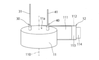
巻回素子10は、図9に示す如く巻回体11を有している。ここで、図9は、後述する製造方法の内、巻回工程の後段の説明に用いられる斜視図である。図9に示す様に、巻回体11は、陽極箔111と陰極箔112とを互いに重ね合わせて巻回することにより構成されている。陽極箔111及び陰極箔112はそれぞれ、アルミニウム、タンタル、ニオブ等の弁作用金属から形成されている。
図示していないが、陽極箔111には、その表面に誘電体被膜が形成されている。一方、図4及び図5に示す如く、陰極箔112には電気絶縁性の繊維シート113が一体化されており、該繊維シート113と陰極箔112とによって1枚の陰極複合シート12が構成されている。ここで、図4は、後述する製造方法の内、一体化工程の説明に用いられる平面図であり、図5は、図4に示されるB-B線に沿う断面図である。図5に示す様に、陰極箔112の両面112a,112bに繊維シート113を貼着固定して固着させることにより、陰極箔112と繊維シート113とが一体化されている。陰極箔112への繊維シート113の貼着には、接着剤や両面テープ等の接着部材(図示せず)が用いられている。又、繊維シート113には、例えばセルロース、アラミド、ポリエステル、ナイロン、ビニロン等の繊維材料から形成された織布又は不織布が用いられている。
尚、陰極箔112の両面112a,112bには、繊維シート113の貼着固定に代えて該両面112a,112bに繊維材料を固着させることにより、繊維シート113となる繊維層が形成されていてもよい。ここで、繊維材料には、セルロース、アラミド、ポリエステル、ナイロン、ビニロン等の材料を用いることが出来る。又、陰極箔112の両面112a,112bには、該両面112a,112bに対して繊維材料を噴き付けることにより、該繊維材料を固着させることが出来る。
図示していないが、巻回体11には固体電解質層が形成されている。ここで、固体電解質層は、巻回体11の内部に形成されている。即ち、巻回体11には、固体電解質層となる電解質が含浸されている。具体的には、固体電解質層を形成するための前駆体、例えば導電性高分子を含んだ重合液を、繊維シート113に含浸させることにより、巻回体11の内部に存在する隙間(主に、陽極箔111と陰極箔112との間に形成された隙間)を埋めた状態で、固体電解質層が形成されている。尚、固体電解質層は、巻回体11の外部、即ち巻回体11の外周面上にも形成されていてもよい。
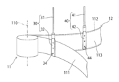
巻回素子10は更に、図8に示す如く陽極リードタブ端子30と陰極リードタブ端子40とを有している(図3も参照)。ここで、図8は、後述する製造方法の内、巻回工程の前段の説明に用いられる斜視図である。陽極リードタブ端子30は、陽極箔111に取り付けられている。一方、陰極リードタブ端子40は、陰極複合シート12に取り付けられている。そして、図9に示す様に、陽極リードタブ端子30と陰極リードタブ端子40は、巻回体11の同じ巻回端面11aから引き出されている。
具体的には、図8に示す様に、陽極リードタブ端子30はリード部31と平坦部32とを有しており、該平坦部32が陽極箔111に取り付けられている。そして、図9に示す様に、陽極リードタブ端子30のリード部31が巻回体11の巻回端面11aから引き出されている。ここで、陽極リードタブ端子30は、その平坦部32を陽極箔111に対して加締めることにより該陽極箔111に取り付けられている。従って、陽極リードタブ端子30は、陽極箔111に電気的に接続されている。尚、陽極箔111に対して陽極リードタブ端子30を加締める方法については、後述する製造方法の第1の端子取付け工程(図6(a)及び図6(b))にて説明する。
一方、図8に示す様に、陰極リードタブ端子40はリード部41と平坦部42とを有しており、該平坦部42が陰極複合シート12に取り付けられている。そして、図9に示す様に、陰極リードタブ端子40のリード部41が巻回体11の巻回端面11aから引き出されている。ここで、陰極リードタブ端子40は、その平坦部42を陰極複合シート12の繊維シート113上に配置すると共に該平坦部42を陰極複合シート12に対して加締めることにより、該陰極複合シート12に取り付けられている。従って、陰極リードタブ端子40は、陰極複合シート12を構成している陰極箔112に電気的に接続されている。尚、陰極複合シート12に対して陰極リードタブ端子40を加締める方法については、後述する製造方法の第2の端子取付け工程(図7(a)及び図7(b))にて説明する。
図3に示す様に、巻回体11において、陽極リードタブ端子30は、巻回軸110とは異なる位置に設けられる一方、陰極リードタブ端子40は、巻回軸110に対して陽極リードタブ端子30とは反対側の位置に設けられている。そして、陽極リードタブ端子30と陰極リードタブ端子40のリード部31,41はそれぞれ、封口部材6を貫通して外装ケース5の外部へ引き出されている。
ここで、図3に示す様に、巻回体11の巻回軸110は、外装ケース5の開口50の中心位置52に略一致している。従って、陽極リードタブ端子30のリード部31は、外装ケース5の開口50の中心位置52とは異なる位置から外装ケース5の外部へ引き出される一方、陰極リードタブ端子40のリード部41は、外装ケース5の開口50の中心位置52に対して陽極リードタブ端子30のリード部31の引出し位置とは反対側の位置から外装ケース5の外部へ引き出されている。
図2及び図3に示す様に、座板2には、該座板2をその上面2aから下面2bに貫通する2つの貫通孔20,20が形成されており、該2つの貫通孔20,20はそれぞれ、座板2の下面2bに設けられている第1溝部201と第2溝部202とに通じている。
そして、陽極リードタブ端子30のリード部31は、これに対応する座板2の貫通孔20を通過した後、該貫通孔20の出口近傍で屈曲し、その後、第1溝部201に沿って第1溝部201内を座板2の縁21まで延びている。そして、該リード部31の内、第1溝部201に沿って第1溝部201内を延びている部分は平坦形状を有しており、該平坦部分によって固体電解コンデンサの陽極端子3が構成されている。
又、陰極リードタブ端子40のリード部41は、これに対応する座板2の貫通孔20を通過した後、該貫通孔20の出口近傍で屈曲し、その後、第2溝部202に沿って第2溝部202内を座板2の縁22まで延びている。そして、該リード部41の内、第2溝部202に沿って第2溝部202内を延びている部分は平坦形状を有しており、該平坦部分によって固体電解コンデンサの陰極端子4が構成されている。
次に、上記固体電解コンデンサの製造方法について、具体的に説明する。該製造方法では、箔作製工程、一体化工程、第1の端子取付け工程、第2の端子取付け工程、巻回工程、再化成処理工程、電解質層形成工程、及び組み立て工程が順に実行される。
箔作製工程では、先ず、陽極箔111となる金属箔を用意する。そして、該金属箔の表面にエッチング加工を施して複数の微細な凹凸を形成し、これによって金属箔の表面積を増大させる。次に、金属箔の表面に対して化成処理を施すことにより、該表面に誘電体被膜を形成する。その後、金属箔に切断加工を施して該金属箔を長尺状の所定形状に裁断する。これにより、表面に誘電体被膜が形成された陽極箔111が作製される。尚、作製された陽極箔111においては、その切断面(端面)に、該陽極箔111を構成する金属の一部が露出することになる。
箔作製工程では更に、陰極箔112となる金属箔を用意する。そして、該金属箔に切断加工を施して金属箔を長尺状の所定形状に裁断する。これにより、陰極箔112が作製される。
一体化工程では、図5に示す様に、陰極箔112の両面112a,112bに繊維シート113を貼着固定して固着させる。これにより、陰極箔112に繊維シート113が一体化され、その結果、繊維シート113と陰極箔112とによって構成された1枚の陰極複合シート12が作製される(図4も参照)。
尚、一体化工程においては、陰極箔112の両面112a,112bに繊維シート113を貼着固定することに代えて、陰極箔112の両面112a,112bに繊維材料を固着させてもよい。これにより、該両面112a,112bには、繊維シート113となる繊維層が形成されることになる。
又、箔作製工程にて陰極箔112を作製する前に、該陰極箔112となる金属箔に対して上記一体化工程を実行してもよい。即ち、金属箔の両面に繊維シート113を貼着固定して固着させ、その後、該金属箔に切断加工を施して金属箔を長尺状の所定形状に裁断してもよい。この場合も、繊維シート113が一体化された陰極箔112(陰極複合シート12)が作製されることになる。
図6(a)及び図6(b)は、第1の端子取付け工程の説明に用いられる平面図である。ここで、第1の端子取付け工程は、陽極箔111に陽極リードタブ端子30を取り付ける工程である。尚、図6(a)は、陽極箔111を陽極リードタブ端子30側から見た平面図である。又、図6(b)は、陽極箔111を陽極リードタブ端子30とは反対側から見た平面図である。図6(a)及び図6(b)に示す様に、第1の端子取付け工程では、陽極リードタブ端子30の平坦部32を陽極箔111に対して加締め、これにより該陽極箔111に陽極リードタブ端子30を取り付ける。
具体的には、陽極リードタブ端子30の平坦部32と陽極箔111とに対して、陽極リードタブ端子30側から加締め針(図示せず)を突き刺す。ここで、加締め針の先端部は、四角錐形状を呈している。従って、加締め針の刺衝により、陽極リードタブ端子30の平坦部32には、図6(a)に示す如く貫通孔34が形成され、更に該平坦部32には、図6(b)に示す如く花弁状のバリ33が、陽極箔111を貫通した状態で形成されることになる。このとき、陽極箔111にもバリが形成されることになる。次に、これらのバリ33に対してプレス加工を施すことにより、バリ33を陽極箔111の表面上にて押し潰す。その結果、陽極リードタブ端子30の平坦部32が陽極箔111に対して加締められることになる。そして、陽極箔111への陽極リードタブ端子30の加締めにより、陽極リードタブ端子30が、陽極箔111に対して電気的に接続されることになる。尚、第1の端子取付け工程では、陽極箔111への陽極リードタブ端子30の加締めにより、誘電体被膜が損傷する虞がある。
図7(a)及び図7(b)は、第2の端子取付け工程の説明に用いられる平面図である。ここで、第2の端子取付け工程は、陰極複合シート12に陰極リードタブ端子40を取り付ける工程である。尚、図7(a)は、陰極複合シート12を陰極リードタブ端子40側から見た平面図である。又、図7(b)は、陰極複合シート12を陰極リードタブ端子40とは反対側から見た平面図である。図7(a)及び図7(b)に示す様に、第2の端子取付け工程では、陰極リードタブ端子40の平坦部42を陰極複合シート12の繊維シート113上に配置すると共に、該平坦部42を陰極複合シート12に対して加締め、これにより該陰極複合シート12に陰極リードタブ端子40を取り付ける。
具体的には、陰極リードタブ端子40の平坦部42と陰極複合シート12とに対して、陰極リードタブ端子40側から加締め針(図示せず)を突き刺す。ここで、加締め針の先端部は、四角錐形状を呈している。従って、加締め針の刺衝により、陰極リードタブ端子40の平坦部42には、図7(a)に示す如く貫通孔44が形成され、更に該平坦部42には、図7(b)に示す如く花弁状のバリ43が、陰極複合シート12を貫通した状態で形成されることになる。このとき、陰極複合シート12を構成している陰極箔112にもバリが形成されることになる。次に、これらのバリ43に対してプレス加工を施すことにより、バリ43を陰極複合シート12の表面上にて押し潰す。その結果、陰極リードタブ端子40の平坦部42が陰極複合シート12に対して加締められることになる。そして、陰極複合シート12への陰極リードタブ端子40の加締めにより、陰極リードタブ端子40が、陰極複合シート12を構成している陰極箔112に対して電気的に接続されることになる。
巻回工程では、図8及び図9に示す様に、陽極箔111と陰極複合シート12とを互いに重ね合わせて巻回し、これにより巻回体11を作製する。このとき、陽極リードタブ端子30と陰極リードタブ端子40とが巻回体11の同じ巻回端面11aから突出することとなる様に、更には、巻回体11において陰極リードタブ端子40が巻回軸110に対して陽極リードタブ端子30とは反対側の位置に配置されることとなる様に、陽極箔111と陰極複合シート12とを重ね合わせて巻回する。そして、陽極箔111の巻回後、巻回体11の型崩れを防止するべく、図9に示す如く巻止めテープ114によって陰極複合シート12の終端部を巻回体11の外周面に固定し、又は、巻止めテープ114によって陽極箔111の終端部を巻回体11の外周面に固定する。巻止めテープ114には、導電性を有したものを用いることが出来る。尚、巻回工程では、陽極箔111の巻回によって誘電体被膜にストレスが生じ、これにより該誘電体被膜が損傷する虞がある。
再化成処理工程では、巻回体11を化成液に浸漬させ、この状態で、陽極リードタブ端子30を通じて陽極箔111に電圧を印加する。ここで、化成液には、例えばアジピン酸アンモニウム水溶液が用いられる。これにより、巻回体11に対して再化成処理が施され、その結果、陽極箔111の切断面(端面)に酸化被膜(誘電体被膜)が形成され、又、誘電体被膜の損傷した部分が修復される。その結果、陽極箔111の表面全体が誘電体被膜によって覆われることになる。
電解質層形成工程では、固体電解質層を形成するための前駆体、例えば導電性高分子を含んだ重合液を用意し、該重合液に巻回体11を浸漬させる。これにより、陰極複合シート12を構成している繊維シート113に重合液が含浸して重合し、これによって巻回体11の内部に存在する隙間(主に、陽極箔111と、陰極複合シート12を構成している陰極箔112との間に形成された隙間)に、該隙間を埋めた状態で導電性高分子膜が形成される。又、巻回体11の外周面上にも導電性高分子膜が形成される。これにより、これらの導電性高分子膜によって固体電解質層が構成され、巻回素子10が完成する。
組み立て工程では、先ず、封口部材6に巻回素子10を固定する(図3参照)。具体的には、封口部材6に対して、陽極リードタブ端子30のリード部31と陰極リードタブ端子40のリード部41とを貫通させる。その後、外装ケース5内に巻回素子10を収容すると共に、外装ケース5の開口50を封口部材6によって塞ぐ。そして、外装ケース5の開口端部に横絞り加工及びカール処理を施すことにより、外装ケース5に封口部材6を固定し、これによって外装ケース5の開口50を封止する。その結果、巻回素子10が外装ケース5内に固定されて、コンデンサ本体1(図1参照)が完成する。
組み立て工程では更に、座板2上にコンデンサ本体1を搭載する(図1~図3参照)。このとき、陽極リードタブ端子30のリード部31を、第1溝部201に通じる貫通孔20に挿入する。又、陰極リードタブ端子40のリード部41を、第2溝部202に通じる貫通孔20に挿入する。
その後、これらのリード部31,41に対して、座板2の下面2bから突出した部分にそれぞれプレス加工を施し、これによって該部分を平坦形状に変形させる。そして、陽極リードタブ端子30のリード部31を貫通孔20の出口近傍にて折り曲げることにより、該リード部31の平坦部分を第1溝部201内に収容する。又、陰極リードタブ端子40のリード部41を貫通孔20の出口近傍にて折り曲げることにより、該リード部41の平坦部分を第2溝部202内に収容する。その結果、リード部31,41の平坦部分によって、座板2の下面2bに露出した陽極端子3と陰極端子4とがそれぞれ構成されることになる。
斯くして、本実施形態の固体電解コンデンサが完成することになる。
上記固体電解コンデンサにおいては、繊維シート113が陰極箔112に一体化されている。このため、図8に示す様に巻回体11を作製する際、陰極箔112と繊維シート113とに対して各々にテンションを掛ける必要がなく、陰極箔112と繊維シート113とが一体化して構成された1枚の陰極複合シート12に対してテンションを掛ければよい。従って、該陰極複合シート12の強度が、巻回時のテンションに耐えることの出来る下限値となるまで、陰極複合シート12の厚さ寸法(陰極箔112と繊維シート113の全体の厚さ寸法)を小さくすることが可能である。よって、上記固体電解コンデンサによれば、陰極箔112と繊維シート113の厚さ寸法をそれぞれ従来の固体電解コンデンサ(図13参照)の陰極箔812とセパレータ813の厚さ寸法より小さくした場合でも、陰極箔112及び繊維シート113を破断させずに巻回体11を作製することが出来る。そこで、陰極箔112及び繊維シート113の厚さ寸法が小さくなった分を陽極箔111に置き換えて陽極箔111の巻回量を増やすことにより、固体電解コンデンサの大容量化と小型化とが実現されることになる。
又、上記固体電解コンデンサによれば、巻回体11を作製する過程において、陽極箔111と陰極複合シート12とを巻回すればよく、このとき新たにセパレータ等の繊維シートを用意して巻回する必要がない。よって、巻回体11の作製が容易である。
本願発明者は、本実施形態に係る固体電解コンデンサ(図3及び図8参照)と、従来の固体電解コンデンサ(図12及び図13参照)とについて、静電容量及びESRを測定する実験を行った。ここで、本実施形態に係る固体電解コンデンサにおいては、陰極箔112に繊維シート113が一体化されているのに対し、従来の固体電解コンデンサにおいては、陰極箔812にセパレータ813が一体化されておらず、本実施形態に係る固体電解コンデンサの陰極箔112と繊維シート113の全体の厚さ寸法が、従来の固体電解コンデンサの陰極箔812とセパレータ813の全体の厚さ寸法より小さくなっている。そして、本実験においては、固体電解コンデンサの外寸を本実施形態と従来のものとで同じにした。又、静電容量の測定周波数を120Hz、ESRの測定周波数を100kHzとした。
実験の結果、従来の固体電解コンデンサにおいて、静電容量が336μF、ESRが12mΩとなったのに対し、本実施形態に係る固体電解コンデンサにおいては、静電容量が653μF、ESRが13mΩとなった。この結果から、本実施形態に係る固体電解コンデンサにおいて大容量化が実現されることが確かめられた。又、本実施形態に係る固体電解コンデンサと従来の固体電解コンデンサとにおいて、これらのESRが同程度になることが確かめられた。又、本願発明者は、陰極箔112と繊維シート113とを一体化して陰極複合シート12を構成することにより、該陰極複合シート12の厚さ寸法を、従来の固体電解コンデンサに用いられる陰極箔又はセパレータの個々の厚さ寸法と同程度又はそれより小さくすることが出来ると考えている。
図10は、上記固体電解コンデンサの変形例について、陰極リードタブ端子40の取付け構造を示した平面図である。又、図11は、図10に示されるC-C線に沿う断面図である。図10及び図11に示す様に、陰極リードタブ端子40は、その平坦部42を陰極複合シート12に貼着固定することにより該陰極複合シート12に取り付けられていてもよい。この構成においては、陰極リードタブ端子40は、陰極複合シート12を構成している繊維シート113に重合液を含浸させて形成される固体電解質層を通じて、陰極箔112に電気的に接続されることになる。
ここで、図11に示す様に、陰極複合シート12への陰極リードタブ端子40の貼着には、接着剤や両面テープ等の接着部材70が用いられる。尚、接着部材70は、導電性のものであってもよいし、電気絶縁性のものであってもよい。但し、接着部材70に導電性のものを用いることにより、陰極複合シート12を構成している繊維シート113に重合液を含浸させて形成される固体電解質層と、陰極リードタブ端子40との電気的な接続面積が増大し、これによって固体電解コンデンサのESRが低減されることになる。
尚、本発明の各部構成は上記実施の形態に限らず、特許請求の範囲に記載の技術的範囲内で種々の変形が可能である。例えば、上記固体電解コンデンサは、陰極箔112の片面112a(又は112b)にのみ繊維シート113が固着されている構成を有していてもよい。この構成を有した固体電解コンデンサを製造する場合、一体化工程においては、陰極箔112の片面112a(又は112b)にのみ繊維シート113が固着されることになる。該構成を有した固体電解コンデンサによれば、巻回体を作製する工程において、陽極箔111と陰極複合シート12とは別にセパレータ等の繊維シートを用意して巻回する必要があったとしても、その枚数は、従来の固体電解コンデンサに比べて少なくて済む。よって、巻回体の作製が容易である。
上記固体電解コンデンサにおいて、巻回体11を構成している陽極箔111及び陰極箔112はそれぞれ、1枚に限らず、2枚以上の複数枚であってもよい。又、上記固体電解コンデンサにおいて、陽極リードタブ端子30及び陰極リードタブ端子40の本数はそれぞれ、1本に限らず、2本以上の複数本であってもよい。
更に、上記固体電解コンデンサにおいて、繊維シート113は、陽極箔111の両面又は片面に固着されることにより、該陽極箔111に一体化されていてもよい。又、上記固体電解コンデンサにおいて、巻回体11が、少なくとも1つの陽極箔111を、該陽極箔111に陰極箔112を重ねずに巻回して構成されたものであり、該陽極箔111に繊維シート113が固着されていてもよい。即ち、上記固体電解コンデンサにおいて、巻回体11が、少なくとも1つの電極箔(陽極箔111や陰極箔112)を巻回することにより構成されており、巻回体11を構成する電極箔の内、少なくとも1つの電極箔の両面又は片面に繊維シート113を固着させることにより、該電極箔に繊維シート113が一体化されていてもよい。
更に又、上記固体電解コンデンサに採用した繊維シート113の一体化構造は、固体電解コンデンサに限らず、電解液タイプの電解コンデンサにも適用することが可能である。
11 巻回体
111 陽極箔
112 陰極箔
113 繊維シート
12 陰極複合シート
30 陽極リードタブ端子
40 陰極リードタブ端子
111 陽極箔
112 陰極箔
113 繊維シート
12 陰極複合シート
30 陽極リードタブ端子
40 陰極リードタブ端子
Claims (7)
- 電極箔を巻回することにより構成された巻回体を備え、前記電極箔には、その両面に電気絶縁性の繊維シートを固着させることにより該繊維シートが一体化されている、電解コンデンサ。
- 前記巻回体は、前記電極箔を複数枚重ね合わせて巻回することにより構成されたものであり、前記繊維シートは、巻回体を構成する複数の電極箔の内、少なくとも1つの電極箔の両面に固着されている、請求項1に記載の電解コンデンサ。
- 前記複数の電極箔には、表面に誘電体被膜が形成された陽極箔と、陰極箔とが含まれ、該陽極箔と陰極箔とを互いに重ね合わせて巻回することにより前記巻回体が構成されており、前記繊維シートは、前記陰極箔の両面に固着されている、請求項2に記載の電解コンデンサ。
- リードタブ端子を更に備え、該リードタブ端子は、前記繊維シート上に配置されると共に、該繊維シートが一体化されている電極箔に電気的に接続されている、請求項1乃至請求項3の何れかに記載の電解コンデンサ。
- 前記繊維シートが一体化されている電極箔において、前記繊維シートは、電極箔の両面に貼着固定されている、請求項1乃至請求項3の何れかに記載の電解コンデンサ。
- 前記繊維シートが一体化されている電極箔において、該電極箔の両面に繊維を固着させることにより、前記繊維シートとなる繊維層が形成されている、請求項1乃至請求項3の何れかに記載の電解コンデンサ。
- 電極箔を用意する工程と、
前記電極箔に対して、該電極箔の少なくとも片面に電気絶縁性の繊維シートを固着させることにより該繊維シートを一体化させる工程と、
前記電極箔に一体化された繊維シート上にリードタブ端子を配置すると共に、該電極箔とリードタブ端子とを互いに電気的に接続する工程と、
前記電極箔を巻回することにより、巻回体を作製する工程と
を有する、電解コンデンサの製造方法。
Priority Applications (1)
| Application Number | Priority Date | Filing Date | Title |
|---|---|---|---|
| JP2012555701A JPWO2012105124A1 (ja) | 2011-01-31 | 2011-12-06 | 電解コンデンサ及びその製造方法 |
Applications Claiming Priority (2)
| Application Number | Priority Date | Filing Date | Title |
|---|---|---|---|
| JP2011017686 | 2011-01-31 | ||
| JP2011-017686 | 2011-01-31 |
Publications (1)
| Publication Number | Publication Date |
|---|---|
| WO2012105124A1 true WO2012105124A1 (ja) | 2012-08-09 |
Family
ID=46602356
Family Applications (1)
| Application Number | Title | Priority Date | Filing Date |
|---|---|---|---|
| PCT/JP2011/078179 Ceased WO2012105124A1 (ja) | 2011-01-31 | 2011-12-06 | 電解コンデンサ及びその製造方法 |
Country Status (2)
| Country | Link |
|---|---|
| JP (1) | JPWO2012105124A1 (ja) |
| WO (1) | WO2012105124A1 (ja) |
Cited By (2)
| Publication number | Priority date | Publication date | Assignee | Title |
|---|---|---|---|---|
| JP2024053309A (ja) * | 2022-10-03 | 2024-04-15 | 株式会社東芝 | 電解コンデンサの製造方法及び電解コンデンサ |
| US20250062078A1 (en) * | 2021-12-28 | 2025-02-20 | Panasonic Intellectual Property Management Co., Ltd. | Electrolytic capacitor and production method for same |
Citations (4)
| Publication number | Priority date | Publication date | Assignee | Title |
|---|---|---|---|---|
| JPH04352313A (ja) * | 1991-05-29 | 1992-12-07 | Matsushita Electric Ind Co Ltd | アルミ電解コンデンサ |
| JP2006049452A (ja) * | 2004-08-03 | 2006-02-16 | Nec Tokin Corp | 電気二重層コンデンサ |
| JP2007201079A (ja) * | 2006-01-25 | 2007-08-09 | Jelmax Co Ltd | 電解コンデンサおよびその製造方法 |
| JP2010225809A (ja) * | 2009-03-23 | 2010-10-07 | Mitsubishi Paper Mills Ltd | 電気化学素子用セパレータ電極一体型蓄電素子およびそれを用いてなる電気化学素子 |
-
2011
- 2011-12-06 WO PCT/JP2011/078179 patent/WO2012105124A1/ja not_active Ceased
- 2011-12-06 JP JP2012555701A patent/JPWO2012105124A1/ja active Pending
Patent Citations (4)
| Publication number | Priority date | Publication date | Assignee | Title |
|---|---|---|---|---|
| JPH04352313A (ja) * | 1991-05-29 | 1992-12-07 | Matsushita Electric Ind Co Ltd | アルミ電解コンデンサ |
| JP2006049452A (ja) * | 2004-08-03 | 2006-02-16 | Nec Tokin Corp | 電気二重層コンデンサ |
| JP2007201079A (ja) * | 2006-01-25 | 2007-08-09 | Jelmax Co Ltd | 電解コンデンサおよびその製造方法 |
| JP2010225809A (ja) * | 2009-03-23 | 2010-10-07 | Mitsubishi Paper Mills Ltd | 電気化学素子用セパレータ電極一体型蓄電素子およびそれを用いてなる電気化学素子 |
Cited By (3)
| Publication number | Priority date | Publication date | Assignee | Title |
|---|---|---|---|---|
| US20250062078A1 (en) * | 2021-12-28 | 2025-02-20 | Panasonic Intellectual Property Management Co., Ltd. | Electrolytic capacitor and production method for same |
| US12688976B2 (en) * | 2021-12-28 | 2026-07-21 | Panasonic Intellectual Property Management Co., Ltd. | Electrolytic capacitor having reduced equivalent series resistance (ESR) and production method for same |
| JP2024053309A (ja) * | 2022-10-03 | 2024-04-15 | 株式会社東芝 | 電解コンデンサの製造方法及び電解コンデンサ |
Also Published As
| Publication number | Publication date |
|---|---|
| JPWO2012105124A1 (ja) | 2014-07-03 |
Similar Documents
| Publication | Publication Date | Title |
|---|---|---|
| US8218293B2 (en) | Winding-type electrolytic capacitor and method of manufacturing the same | |
| CN103971938A (zh) | 电解电容器 | |
| JP2010153701A (ja) | 電解コンデンサ | |
| US20110122547A1 (en) | Electrolytic capacitor and manufacturing method thereof | |
| KR101434923B1 (ko) | 고체 전해 컨덴서 | |
| JP5945727B2 (ja) | 固体電解コンデンサ | |
| JPWO2012105124A1 (ja) | 電解コンデンサ及びその製造方法 | |
| CN104321843B (zh) | 电解电容器 | |
| CN116072430A (zh) | 电解电容器及其制造方法 | |
| JP5775040B2 (ja) | 固体電解コンデンサ | |
| JP5903611B2 (ja) | 固体電解コンデンサ | |
| JP2009026853A (ja) | 電気二重層キャパシタ | |
| JP5054610B2 (ja) | 巻回型電解コンデンサの製造方法 | |
| JP2010074089A (ja) | 電解コンデンサおよびその製造方法 | |
| JP5886766B2 (ja) | 固体電解コンデンサ | |
| JP6948555B2 (ja) | 電解コンデンサおよびその製造方法 | |
| JP4798478B2 (ja) | 電解コンデンサ | |
| JP2012069631A (ja) | 電解コンデンサ | |
| JP2020191373A (ja) | 巻回形蓄電デバイスおよびその製造方法 | |
| JP3582542B2 (ja) | 電気二重層コンデンサ素子およびその製造方法 | |
| WO2012086407A1 (ja) | 固体電解コンデンサ及びその製造方法 | |
| JP2006286959A (ja) | 電解コンデンサ | |
| JP2008098675A (ja) | 偏平形金属化フィルムコンデンサ | |
| JP4900765B2 (ja) | 電解コンデンサ | |
| JP4953043B2 (ja) | 電解コンデンサ |
Legal Events
| Date | Code | Title | Description |
|---|---|---|---|
| 121 | Ep: the epo has been informed by wipo that ep was designated in this application |
Ref document number: 11857521 Country of ref document: EP Kind code of ref document: A1 |
|
| ENP | Entry into the national phase |
Ref document number: 2012555701 Country of ref document: JP Kind code of ref document: A |
|
| NENP | Non-entry into the national phase |
Ref country code: DE |
|
| 122 | Ep: pct application non-entry in european phase |
Ref document number: 11857521 Country of ref document: EP Kind code of ref document: A1 |