WO2012090858A1 - 静電チャック装置 - Google Patents
静電チャック装置 Download PDFInfo
- Publication number
- WO2012090858A1 WO2012090858A1 PCT/JP2011/079814 JP2011079814W WO2012090858A1 WO 2012090858 A1 WO2012090858 A1 WO 2012090858A1 JP 2011079814 W JP2011079814 W JP 2011079814W WO 2012090858 A1 WO2012090858 A1 WO 2012090858A1
- Authority
- WO
- WIPO (PCT)
- Prior art keywords
- electrostatic chuck
- temperature
- temperature adjusting
- sintered body
- electrostatic
- Prior art date
- Legal status (The legal status is an assumption and is not a legal conclusion. Google has not performed a legal analysis and makes no representation as to the accuracy of the status listed.)
- Ceased
Links
Images
Classifications
-
- H—ELECTRICITY
- H10—SEMICONDUCTOR DEVICES; ELECTRIC SOLID-STATE DEVICES NOT OTHERWISE PROVIDED FOR
- H10P—GENERIC PROCESSES OR APPARATUS FOR THE MANUFACTURE OR TREATMENT OF DEVICES COVERED BY CLASS H10
- H10P72/00—Handling or holding of wafers, substrates or devices during manufacture or treatment thereof
- H10P72/04—Apparatus for manufacture or treatment
- H10P72/0431—Apparatus for thermal treatment
- H10P72/0434—Apparatus for thermal treatment mainly by convection
-
- H—ELECTRICITY
- H10—SEMICONDUCTOR DEVICES; ELECTRIC SOLID-STATE DEVICES NOT OTHERWISE PROVIDED FOR
- H10P—GENERIC PROCESSES OR APPARATUS FOR THE MANUFACTURE OR TREATMENT OF DEVICES COVERED BY CLASS H10
- H10P72/00—Handling or holding of wafers, substrates or devices during manufacture or treatment thereof
- H10P72/70—Handling or holding of wafers, substrates or devices during manufacture or treatment thereof for supporting or gripping
- H10P72/72—Handling or holding of wafers, substrates or devices during manufacture or treatment thereof for supporting or gripping using electrostatic chucks
Definitions
- the present invention relates to an electrostatic chuck device, and more specifically, a semiconductor manufacturing process technique in which a plate-like sample such as a semiconductor wafer is adsorbed and fixed by electrostatic force, in particular, ions are implanted into a plate-like sample such as a single crystal silicon wafer.
- the present invention relates to an electrostatic chuck device suitable for use in an ion implantation process.
- the electrostatic chuck is a substrate on which an object to be attracted placed on the electrostatic chuck can be electrically fixed by supplying electricity from the outside to an electrode embedded therein.
- an ion implantation method is used as a method for introducing impurities into a single crystal silicon wafer. Since this ion implantation method can control the impurity concentration and impurity distribution in the silicon wafer, the ion implantation method is mainly used particularly in a semiconductor manufacturing process such as VLSI.
- an ion implantation apparatus having a cooling mechanism capable of cooling a silicon wafer at the time of ion implantation is used (for example, see Patent Document 1).
- the conventional ion implantation apparatus described above has an advantage of doping impurities into the silicon wafer in a controlled manner in order to implant high energy impurity ions into the single crystal silicon wafer.
- problems such as amorphization of single crystal silicon during ion implantation and distortion of the crystal lattice may occur.
- This amorphization of the silicon wafer proceeds non-uniformly. Therefore, in the semiconductor manufacturing process after ion implantation, the crystal lattice is distorted or lattice defects occur in the silicon wafer even after annealing for activation due to non-uniform amorphization. There is a problem in that damage at the lattice level occurs, and this damage at the lattice level causes abnormal leakage current (leakage current) in the final product.
- an ion implantation process is performed in a state where the ion implantation apparatus is cooled with liquid nitrogen as a method for preventing non-uniform progression of the amorphousization of the silicon wafer and suppressing damage at the lattice level during ion implantation.
- This method can suppress damage to the silicon wafer at the time of ion implantation, and by advancing the amorphousization of the silicon wafer uniformly without damage, the silicon wafer can be reactivated along with the activation of the implanted ions.
- the annealing temperature for crystallization can be lowered.
- the electrostatic chuck device that fixes the silicon wafer at the time of ion implantation is also cooled by liquid nitrogen.
- condensation occurs on the back surface, and in order to prevent this dew condensation, there is a problem that it is necessary to take a large measure of condensation on the back surface side. .
- the present invention has been made in view of the above circumstances, and in performing a low temperature region ion implantation process, it is possible to suppress damage in a plate sample such as a silicon wafer during ion implantation, and Amorphization of the sample can be progressed uniformly without damage. Moreover, it is an object of the present invention to provide an electrostatic chuck device that does not cause condensation even when the back surface is exposed to the atmosphere.
- an electrostatic chuck portion on which a plate-like sample is placed and a temperature adjustment base portion that adjusts the temperature of the electrostatic chuck portion If a temperature adjusting base material is provided in between, and a flow path for flowing a cooling medium is formed in the temperature adjusting base material, when performing a low temperature region ion implantation process, a silicon wafer at the time of ion implantation, etc. It is possible to suppress the damage in the plate-like sample and to allow the amorphization of the plate-like sample to proceed uniformly without damage, and there is a possibility that condensation occurs even when the back surface is exposed to the atmosphere. The present inventors have found that there is not, and have completed the present invention.
- the electrostatic chuck device of the present invention has an electrostatic chuck portion in which one main surface is a mounting surface on which a plate-like sample is placed and an internal electrode for electrostatic attraction is built in, and other electrostatic chuck portions. And a temperature adjusting base portion that adjusts the electrostatic chuck portion to a desired temperature, and a temperature adjusting base material between the electrostatic chuck portion and the temperature adjusting base portion. And a flow path for allowing the cooling medium to flow is formed in the temperature adjusting base material.
- the flow path is a groove formed on a main surface on the electrostatic chuck portion side of the temperature adjusting substrate.
- the electrostatic chuck portion and the temperature adjusting base material are bonded and fixed via a low temperature compatible organic adhesive.
- the low temperature compatible organic adhesive is preferably an epoxy adhesive.
- the electrostatic chuck portion is made of any one or more of an aluminum oxide-silicon carbide composite sintered body, an aluminum oxide sintered body, an aluminum nitride sintered body, and an yttrium oxide sintered body.
- the temperature adjusting substrate is made of any one of an aluminum oxide sintered body, an aluminum nitride sintered body, and an yttrium oxide sintered body.
- the electrostatic chuck portion may be composed of one or more of an aluminum oxide-silicon carbide composite sintered body, an aluminum oxide sintered body, an aluminum nitride sintered body, and an yttrium oxide sintered body.
- the temperature adjusting substrate is preferably made of any one of an aluminum oxide sintered body, an aluminum nitride sintered body, and an yttrium oxide sintered body.
- the electrostatic chuck portion, the temperature adjustment base material, and the temperature adjustment base portion are superposed in this order, and are pressurized and held at 80 ° C. or higher and 100 ° C. or lower in the atmosphere. These are bonded and integrated.
- the manufacturing method of the electrostatic chuck device of the present invention includes a step of applying a low temperature compatible organic adhesive to the surface of the electrostatic chuck portion to which the temperature adjusting substrate is bonded, and a temperature adjusting base portion of the temperature adjusting substrate. It is preferable to include a step of applying an adhesive to the surface where the adhesive is adhered.
- the temperature adjustment base material in which the flow path for flowing the cooling medium is provided between the electrostatic chuck portion and the temperature adjustment base portion. Therefore, even when the electrostatic chuck part is cooled to the temperature of the cooling medium, the temperature adjustment base part is insulated from the electrostatic chuck part by the temperature adjustment base material, so that the temperature of the back surface of the temperature adjustment base part can be reduced. It can be maintained at about room temperature (25 ° C. to 20 ° C.). Therefore, even when the electrostatic chuck portion is cooled to the temperature of the cooling medium by the temperature adjustment base material, the temperature of the back surface of the electrostatic chuck device is set to room temperature (25 ° C. to 20 ° C.) by the temperature adjustment base portion. Even when exposed to the atmosphere, there is no possibility that condensation occurs on the back surface.
- a main surface means two surfaces with a large area among the surfaces which comprise an electrostatic chuck part or the temperature control base material.
- the electrostatic chuck and the temperature adjustment substrate are bonded and fixed via a low temperature compatible organic adhesive, the electrostatic chuck is cooled to the temperature of the cooling medium by the temperature adjustment substrate.
- the adhesive strength between the electrostatic chuck portion and the temperature adjusting substrate can be maintained, and there is no possibility of peeling or the like.
- the low temperature compatible organic adhesive is an epoxy adhesive
- the electrostatic chuck portion and the temperature adjusting substrate The adhesive strength between the two can be sufficiently maintained, and there is no possibility of peeling.
- the electrostatic chuck portion is one or more of an aluminum oxide-silicon carbide composite sintered body, an aluminum oxide sintered body, an aluminum nitride sintered body, and an yttrium oxide sintered body.
- an aluminum oxide sintered body, an aluminum nitride sintered body, and an yttrium oxide sintered body was used. Therefore, durability in a semiconductor manufacturing process such as ion implantation can be improved, and mechanical strength can be maintained.
- the electrostatic chuck portion is provided by providing a temperature adjustment base material in which a flow path for flowing the cooling medium is provided between the electrostatic chuck portion and the temperature adjustment base portion. Is cooled to the temperature of the cooling medium by the temperature adjusting base material, and the temperature adjusting base portion is bonded and fixed to the electrostatic chuck portion via the temperature adjusting base material, The heat is insulated from the electrostatic chuck portion, and the temperature of the back surface thereof is maintained at about room temperature (25 ° C. to 20 ° C.).
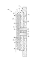
- FIG. 1 is a cross-sectional view showing an electrostatic chuck device according to a first embodiment of the present invention.
- the electrostatic chuck device 1 includes a disk-shaped electrostatic chuck portion 2 and an electrostatic chuck portion 2.
- the electrostatic chuck unit 2 supports the mounting plate 11 which is integrated with the mounting plate 11 whose upper surface is a mounting surface 11a on which a plate-like sample W such as a semiconductor wafer is mounted.
- a large number of protrusions 16 are formed on the mounting surface of the mounting plate 11, and these protrusions 16 are configured to support the plate-like sample W.
- the mounting plate 11 and the support plate 12 are disk-shaped with the same shape of the superimposed surfaces, and are an aluminum oxide-silicon carbide (Al 2 O 3 -SiC) composite sintered body, aluminum oxide (Al 2 It has mechanical strength such as O 3 ) sintered body, aluminum nitride (AlN) sintered body, yttrium oxide (Y 2 O 3 ) sintered body, and durability in semiconductor manufacturing processes such as ion implantation process. It consists of an insulating ceramic sintered body.
- the material of the mounting plate 11 and the support plate 12 is not particularly limited as long as each function can be sufficiently exhibited.
- the mounting plate 11 is made of aluminum oxide-silicon carbide (Al 2 O 3).
- the total thickness of the mounting plate 11, the support plate 12, the electrostatic adsorption internal electrode 13 and the insulating material layer 14, that is, the thickness of the electrostatic chuck portion 2 is preferably 1.0 mm or more and 10 mm or less, and 3.0 mm. More preferably, it is 4.0 mm or less. The reason is that if the thickness of the electrostatic chuck portion 2 is less than 1.0 mm, the mechanical strength of the electrostatic chuck portion 2 cannot be ensured, while the thickness of the electrostatic chuck portion 2 exceeds 10 mm.
- the heat capacity of the electrostatic chuck portion 2 becomes too large, the thermal responsiveness of the plate-like sample W to be mounted deteriorates, and further, the plate-like sample is increased due to an increase in the lateral heat transfer of the electrostatic chuck portion. This is because it becomes difficult to maintain the in-plane temperature of W in a desired temperature pattern.
- the thickness of the mounting plate 11 is preferably 1.0 mm or more and 4.0 mm or less. The reason is that if the thickness of the mounting plate 11 is less than 1.0 mm, the risk of discharge is increased by the voltage applied to the internal electrode 13 for electrostatic attraction, while if it exceeds 4.0 mm, the plate-like sample is increased. This is because W cannot be sufficiently adsorbed and fixed.
- the internal electrode 13 for electrostatic adsorption is used as an electrode for an electrostatic chuck for generating a charge and fixing the plate-like sample W with an electrostatic adsorption force. Adjust as appropriate.
- the internal electrode 13 for electrostatic adsorption is composed of an aluminum oxide-tantalum carbide (Al 2 O 3 —Ta 4 C 5 ) conductive composite sintered body, an aluminum oxide-tungsten (Al 2 O 3 —W) conductive composite sintered body.
- Al 2 O 3 -SiC aluminum oxide-silicon carbide
- AlN-W aluminum nitride-tungsten
- AlN-Ta aluminum nitride-tantalum
- sintered ceramics conductive ceramics such as yttrium oxide-molybdenum (Y 2 O 3 -Mo) conductive composite sintered bodies, or refractory metals such as tungsten (W), tantalum (Ta), molybdenum (Mo) Is formed.
- the thickness of the internal electrode 13 for electrostatic adsorption is not particularly limited, but is preferably 5 ⁇ m or more and 50 ⁇ m or less, and particularly preferably 20 ⁇ m or more and 40 ⁇ m or less. The reason is that if the thickness is less than 5 ⁇ m, sufficient conductivity cannot be ensured. On the other hand, if the thickness exceeds 50 ⁇ m, the electrostatic adsorption internal electrode 13, the mounting plate 11, and the support plate 12 This is because cracks are likely to occur at the joint interface between the electrostatic attraction internal electrode 13 and the mounting plate 11 and the support plate 12 due to the difference in thermal expansion coefficient between them.
- the electrostatic adsorption internal electrode 13 having such a thickness can be easily formed by a film forming method such as a sputtering method or a vapor deposition method, or a coating method such as a screen printing method.
- the insulating material layer 14 surrounds the electrostatic adsorption internal electrode 13 to protect the electrostatic adsorption internal electrode 13 from the atmosphere during ion implantation and the like, and at the boundary portion between the mounting plate 11 and the support plate 12, that is, The outer peripheral region other than the internal electrode 13 for electrostatic attraction is joined and integrated, and is composed of the same composition or the main component of the same material as that of the mounting plate 11 and the support plate 12 and the same insulating material.
- the power feeding terminal 15 is a rod-shaped member provided to apply a DC voltage to the electrostatic adsorption internal electrode 13.
- the material of the power supply terminal 15 is not particularly limited as long as it is a conductive material having excellent heat resistance, but the thermal expansion coefficient is equal to the thermal expansion coefficient of the electrostatic adsorption internal electrode 13 and the support plate 12. Approximate ones are preferable, for example, conductive ceramics constituting the internal electrode 13 for electrostatic adsorption, or tungsten (W), tantalum (Ta), molybdenum (Mo), niobium (Nb), Kovar alloy, etc. A metal material is preferably used.
- the power feeding terminal 15 is insulated from the temperature adjusting base portion 3 and the temperature adjusting base material 4 by an insulator 17 having insulating properties.
- the power feeding terminal 15 is joined and integrated with the support plate 12, and the mounting plate 11 and the support plate 12 are joined and integrated by the electrostatic attraction internal electrode 13 and the insulating material layer 14, and the electrostatic chuck portion. 2 is constituted.
- the temperature adjusting base 3 adjusts the electrostatic chuck 2 to a desired temperature, and has a thick disk shape.
- this temperature adjustment base part 3 for example, a water-cooled base in which a flow path 21 for circulating water is formed is suitable.
- a concave portion 22 for fitting the temperature adjusting base material 4 is formed on the upper surface of the temperature adjusting base portion 3.
- the material constituting the temperature adjusting base 3 is not particularly limited as long as it is a metal excellent in thermal conductivity, conductivity, and workability, or a composite material containing these metals.
- a metal excellent in thermal conductivity, conductivity, and workability or a composite material containing these metals.
- aluminum (Al) Aluminum alloy, copper (Cu), copper alloy, stainless steel (SUS), etc. are preferably used. It is preferable that at least the surface of the temperature adjusting base portion 3 exposed to the atmosphere during ion implantation or the like is subjected to an alumite treatment or an insulating film such as alumina is formed.
- the substrate 4 for temperature adjustment cools the electrostatic chuck part 2 to a desired temperature using a cooling medium such as liquid nitrogen, has a disk shape larger in diameter than the electrostatic chuck part 2, and is made of aluminum oxide (Al 2 O 3 ) It has mechanical strength such as sintered body, aluminum nitride (AlN) sintered body, yttrium oxide (Y 2 O 3 ) sintered body, and durability in semiconductor manufacturing processes such as ion implantation process. It consists of an insulating ceramic sintered body.
- a concave portion 31 for fitting the electrostatic chuck portion 2 is formed on the upper surface (main surface) of the temperature adjusting substrate 4, and a groove 32 for flowing a cooling medium such as liquid nitrogen is formed on the bottom surface of the concave portion 31. Is formed.
- the electrostatic chuck portion is efficiently cooled by the cooling medium flowing in the groove formed on the main surface of the temperature adjusting base material.
- the pattern shape of the groove 32 is not particularly limited as long as the electrostatic chuck unit 2 can be cooled to a desired temperature using a cooling medium such as liquid nitrogen, but the lower surface of the electrostatic chuck unit 2 is made uniform.
- a spiral shape or a meandering shape is preferable in that it can be cooled.
- the thickness of the temperature adjusting substrate 4 is preferably 5 mm or more and 30 mm or less, and more preferably 10 mm or more and 20 mm or less. The reason for this is that when the thickness of the temperature adjusting substrate 4 is less than 5 mm, the mechanical strength of the temperature adjusting substrate 4 is reduced and the heat insulation between the electrostatic chuck portion 2 and the temperature adjusting base portion 3 is performed. As a result, the temperature controllability in the electrostatic chuck portion 2 is lowered, and it becomes difficult to maintain the in-plane temperature of the plate-like sample W in a desired temperature pattern.
- the thickness of the temperature adjusting substrate 4 exceeds 30 mm, heat transfer between the electrostatic chuck portion 2 and the temperature adjusting base portion 3 is ensured, although the mechanical strength of the temperature adjusting substrate 4 is ensured. As a result, the controllability of the temperature in the electrostatic chuck portion 2 is lowered, and it becomes difficult to maintain the in-plane temperature of the plate-like sample W in a desired temperature pattern.
- the low-temperature-compatible organic adhesive layer 5 has an insulating property for bonding and fixing the electrostatic chuck portion 2 cooled by using a cooling medium such as liquid nitrogen and the temperature adjusting substrate 4, and has a heat resistant temperature. It is made of an adhesive having a temperature of ⁇ 270 ° C. or higher and 120 ° C. or lower. As a result, even when the electrostatic chuck portion is cooled to the temperature of the cooling medium by the temperature adjusting substrate, the adhesive strength between the electrostatic chuck portion and the temperature adjusting substrate is maintained, and there is a risk of peeling or the like. No. As a material for the low temperature compatible organic adhesive layer 5, an epoxy adhesive having heat resistance in the above temperature range is preferably used. As a result, even when the electrostatic chuck portion is cooled to the temperature of the cooling medium by the temperature adjusting substrate, the adhesive strength between the electrostatic chuck portion and the temperature adjusting substrate is sufficiently maintained, and peeling or the like is prevented. No.
- the thickness of the low-temperature-compatible organic adhesive layer 5 is preferably 50 ⁇ m or more and 300 ⁇ m or less, more preferably 75 ⁇ m, considering the rapidity of heat transfer between the electrostatic chuck portion 2 and the temperature adjusting substrate 4. Above and below 125 ⁇ m.
- the in-plane thickness variation of the low temperature compatible organic adhesive layer 5 is preferably within 10 ⁇ m.
- the in-plane thickness variation of the low-temperature-compatible organic adhesive layer 5 exceeds 10 ⁇ m, the in-plane spacing between the electrostatic chuck portion 2 and the temperature adjustment substrate 4 exceeds 10 ⁇ m.
- the in-plane uniformity of the cold transmitted from the temperature adjusting substrate 4 to the electrostatic chuck unit 2 is reduced, and the in-plane temperature on the mounting surface of the electrostatic chuck unit 2 becomes non-uniform. .
- the adhesive layer 6 has an insulating property for bonding and fixing the temperature adjusting substrate 4 and the temperature adjusting base 3, and is made of an adhesive having a heat resistant temperature of ⁇ 100 ° C. or more and 120 ° C. or less.
- an adhesive having a heat resistant temperature of ⁇ 100 ° C. or more and 120 ° C. or less.
- a silicone adhesive, a polyimide adhesive, an epoxy adhesive, etc. having heat resistance in the above temperature range are preferable, and a siloxane bond (Si—O—Si) is particularly preferable.
- a silicone adhesive having a heat resistant temperature of ⁇ 50 ° C. or higher and 100 ° C. or lower is preferable.
- This silicone-based adhesive is an adhesive excellent in heat resistance and elasticity, and can be represented by, for example, a chemical formula of the following formula (1) or formula (2).
- R is, H or an alkyl group (C n H 2n + 1 - : n is an integer) is.
- R is, H or an alkyl group (C n H 2n + 1 - : n is an integer) is.
- an adhesive having a Young's modulus after curing of 8 MPa or less is preferable.
- the Young's modulus after curing exceeds 8 MPa, the thermal expansion of the temperature adjusting base material 4 and the temperature adjusting base portion 3 occurs when the adhesive layer 6 is subjected to a heat cycle of increasing and decreasing temperatures. Since the difference cannot be absorbed and the durability of the adhesive layer 6 is lowered, it is not preferable.
- the thickness of the adhesive layer 6 is preferably not less than 50 ⁇ m and not more than 300 ⁇ m, more preferably not less than 100 ⁇ m and not more than 200 ⁇ m, considering heat insulation and stress relaxation between the temperature adjusting base portion 3 and the temperature adjusting base material 4. It is.
- Al 2 O 3 —SiC aluminum oxide-silicon carbide
- AlN aluminum nitride
- Y 2 O 3 yttrium oxide
- a mixed powder containing silicon carbide powder and aluminum oxide powder, aluminum oxide powder, aluminum nitride powder, or yttrium oxide powder is formed into a desired shape, and then in a preferable atmosphere for the powder,
- the mounting plate 11 and the support plate 12 can be obtained by baking at a temperature of 1400 ° C. to 2000 ° C. for a predetermined time.
- a plurality of fixing holes for fitting and holding the power feeding terminal 15 and the insulator 17 are formed in the support plate 12.
- the fixing hole may be formed when the powder is molded.
- a coating liquid for forming an internal electrode for electrostatic adsorption in which a conductive material such as the above conductive ceramic powder is dispersed in an organic solvent is prepared, and the coating liquid for forming an internal electrode for electrostatic adsorption is applied to the mounting plate 11. It is applied to a predetermined area on the back surface and dried to form an electrostatic adsorption internal electrode forming layer.
- this coating method it is desirable to use a screen printing method or the like because it is necessary to apply the film to a uniform thickness.
- a method other than the above-described coating method there is a method in which a thin plate made of the above-described conductive ceramics is disposed to form an internal electrode forming layer for electrostatic adsorption.
- a high melting point metal such as tungsten (W), tantalum (Ta), molybdenum (Mo), niobium (Nb), Kovar alloy or the like is used for the electrostatic adsorption internal electrode formation layer
- a vapor deposition method or a sputtering method is used.
- an insulating material is formed on the mounting plate 11 other than the region where the internal electrode forming layer for electrostatic attraction is formed, including a powder material having the same composition or the same main component as the mounting plate 11 and the support plate 12.
- the insulating material forming layer is formed by applying a coating liquid in which a powder made of an insulating material having the same composition or the same main component as the mounting plate 11 and the support plate 12 is dispersed in an organic solvent by screen printing or the like in the predetermined area. It can be formed by applying and drying.
- the support plate 12 is overlaid on the electrostatic adsorption internal electrode forming layer and the insulating material forming layer on the mounting plate 11, and then these are hot-pressed under high temperature and high pressure to be integrated.
- the atmosphere in this hot press is preferably a vacuum or an inert atmosphere such as Ar, He, N 2 or the like.
- the pressure during uniaxial pressing in the hot press is preferably 5 to 10 MPa, and the temperature is preferably 1400 ° C. to 1850 ° C.
- the internal electrode forming layer for electrostatic adsorption is fired to become the internal electrode 13 for electrostatic adsorption made of a conductive composite sintered body.
- the insulating material forming layer is also baked to form the insulating material layer 14, and the support plate 12 and the mounting plate 11 are joined and integrated by the insulating material layer 14.
- the upper and lower surfaces, outer periphery, gas holes (not shown) and the like of these joined bodies are machined to form the electrostatic chuck portion 2.
- This gas hole is a hole formed in the electrostatic chuck portion 2 so that a cooling gas such as helium described later flows between the mounting plate 11 and the plate-like sample W.
- the power supply terminal 15 is manufactured so as to have a size and a shape that can be tightly fixed to the fixing hole of the support plate 12.
- a method for producing the power supply terminal 15 for example, when the power supply terminal 15 is made of a conductive composite sintered body, a method of forming a conductive ceramic powder into a desired shape and pressurizing and firing can be cited.
- the conductive ceramic powder used for the power feeding terminal 15 is preferably a conductive ceramic powder made of the same material as the internal electrode 13 for electrostatic adsorption.
- a method of using a refractory metal and a metal working method such as a grinding method or powder metallurgy, or the like can be used.
- a metal material made of aluminum (Al), aluminum alloy, copper (Cu), copper alloy, stainless steel (SUS), etc. is machined, and water is circulated inside the metal material as necessary.
- a path or the like is formed, and further, a fixing hole for fitting and holding the power supply terminal 15 and the insulator 17 is formed, and the temperature adjusting base portion 3 is formed. It is preferable to perform alumite treatment or form an insulating film such as alumina on at least the surface of the temperature adjusting base portion 3 exposed to the atmosphere during ion implantation.
- a plurality of fixing holes for fitting and holding the power supply terminal 15 and the insulator 17 are formed in the temperature adjusting base portion 3.
- the temperature adjusting substrate 4 having a desired shape is formed.
- an aluminum oxide (Al 2 O 3 ) powder, an aluminum nitride powder, or an yttrium oxide powder is formed into a desired shape, and then, for example, at a temperature of 1400 ° C. to 2000 ° C. in a preferable atmosphere for the powder.
- the substrate is baked for a predetermined time to obtain a temperature adjusting substrate 4.
- a plurality of fixing holes for fitting and holding the power supply terminals 15 and the insulators 17 are formed in the temperature adjusting substrate 4.
- the fixing hole may be formed when the powder is molded.
- the lower surface of the support plate 12 of the electrostatic chuck unit 2, that is, the surface to which the temperature adjustment base material 4 is bonded is degreased and washed using, for example, acetone.
- An epoxy adhesive having a heat resistant temperature of ⁇ 270 ° C. or higher and 120 ° C. or lower is applied by a coating method so as to have a thickness of 100 ⁇ m or more and 200 ⁇ m or less.
- the lower surface of the temperature adjusting substrate 4, that is, the surface to which the temperature adjusting base portion 3 is bonded is degreased and washed using, for example, acetone, and a coating method such as a screen printing method is applied to a predetermined region on this surface.
- a silicone adhesive, polyimide adhesive, or epoxy adhesive having a heat resistant temperature of ⁇ 100 ° C. or more and 120 ° C. or less is applied so as to have a thickness of 200 ⁇ m or more and 300 ⁇ m or less.
- the electrostatic chuck part 2, the temperature adjusting base material 4 and the temperature adjusting base part 3 are superposed in this order.
- the power supply terminal 15 and the insulator 17 are inserted and fitted into a power supply terminal accommodation hole (not shown) drilled in the temperature adjustment base 3 and the temperature adjustment base material 4.
- the electrostatic chuck part 2, the temperature adjusting base material 4, the temperature adjusting base part 3, the power feeding terminal 15 and the insulator 17 are pressurized and held at 80 ° C. or higher and 100 ° C. or lower in the atmosphere. Are bonded and integrated.
- the epoxy adhesive applied to the lower surface of the support plate 12 is cured to become a low temperature compatible organic adhesive layer 5, and a silicone adhesive applied to the lower surface of the temperature adjusting substrate 4, The polyimide adhesive or the epoxy adhesive is cured to form the adhesive layer 6.
- the electrostatic chuck portion 2 As described above, the electrostatic chuck portion 2, the temperature adjustment base material 4, the temperature adjustment base portion 3, the power feeding terminal 15 and the insulator 17 are joined and integrated through the low temperature compatible organic adhesive layer 5 and the adhesive layer 6. Thus, the electrostatic chuck device 1 of this embodiment is obtained.
- a temperature adjusting groove in which a groove 32 for allowing a cooling medium to flow is formed in the concave portion 31 on the electrostatic chuck portion 2 side between the electrostatic chuck portion 2 and the temperature adjusting base portion 3. Since the substrate 4 is provided, the temperature adjustment base 3 can be insulated from the electrostatic chuck 2 by the temperature adjustment substrate 4 even when the electrostatic chuck 2 is cooled to the temperature of the cooling medium. The temperature of the lower surface of the temperature adjusting base 3 can be maintained at about room temperature (25 ° C. to 20 ° C.).
- the temperature of the back surface of the electrostatic chuck device 1 is changed to the room temperature (25 ° C.) by the temperature adjustment base portion 3. It can be kept at a temperature of about 20 ° C.), and even when exposed to the atmosphere, there is no risk of condensation on the back surface.
- the electrostatic chuck portion 2 and the temperature adjustment base material 4 are bonded and fixed via the low temperature compatible organic adhesive layer 5, the electrostatic chuck portion 2 is attached to the cooling medium by the temperature adjustment base material 4. Even when cooled to the temperature, the adhesive strength between the electrostatic chuck portion 2 and the temperature adjusting substrate 4 can be maintained, and there is no possibility of peeling or the like.
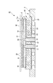
- FIG. 2 is a cross-sectional view showing an electrostatic chuck device according to a second embodiment of the present invention.
- the electrostatic chuck device 41 is different from the electrostatic chuck device 1 of the first embodiment in that, in the electrostatic chuck device 1 of the first embodiment, an electrostatic chuck portion is provided on the upper surface of the temperature adjusting substrate 4. 2 is formed, and a groove 32 for flowing a cooling medium such as liquid nitrogen is formed on the bottom surface of the recess 31, whereas the electrostatic chuck device 41 of the present embodiment has a static surface on the top surface.
- the pattern shape of the flow path 43 is not particularly limited as long as the electrostatic chuck unit 2 can be cooled to a desired temperature using a cooling medium such as liquid nitrogen, but the lower surface of the electrostatic chuck unit 2 is uniform. From the viewpoint of being able to be cooled to a low temperature, a spiral shape or a meandering shape is preferable.
- This electrostatic chuck device 41 can also provide the same operations and effects as the electrostatic chuck device 1 of the first embodiment.
- the flow path 43 for flowing a cooling medium such as liquid nitrogen is formed inside the temperature adjusting base material 42 in which the recess 31 for fitting the electrostatic chuck portion 2 is formed on the upper surface, this flow path is formed. By causing the cooling medium to flow through 43, the electrostatic chuck portion 2 can be efficiently cooled by the cooling medium.
- An electrostatic chuck portion 2 in which an internal electrode 13 for electrostatic attraction having a thickness of 30 ⁇ m was embedded was produced by a known method.
- the mounting plate 11 of the electrostatic chuck portion 2 is an aluminum oxide-silicon carbide composite sintered body containing 8% by mass of silicon carbide, and has a disk shape with a diameter of 200 mm and a thickness of 2 mm. Further, the electrostatic chucking surface of the mounting plate 11 is formed as an uneven surface by forming a large number of protrusions 16 having a height of 30 ⁇ m, and the top surface of these protrusions 16 is used as a holding surface for the plate-like sample W.
- the cooling gas can be made to flow in a groove formed between the recess and the electrostatically adsorbed plate-like sample W.
- the support plate 12 is an aluminum oxide-silicon carbide composite sintered body containing 8% by mass of silicon carbide, and has a disk shape with a diameter of 200 mm and a thickness of 2 mm. By joining and integrating the mounting plate 11 and the support plate 12, the entire thickness of the electrostatic chuck portion 2 was 4 mm.
- an aluminum temperature adjusting base 3 having a diameter of 250 mm and a height of 20 mm was produced by machining.
- a flow path (not shown) for circulating the refrigerant was formed inside the temperature adjusting base 3.
- the temperature adjusting substrate 4 had a disk shape with a diameter of 220 mm and a thickness of 15 mm. Further, a spiral groove 32 having a depth of 25 mm and a width of 12 mm is formed in the concave portion 31 on the upper surface of the temperature adjusting substrate 4 so that a cooling medium such as liquid nitrogen can flow.
- the lower surface of the support plate 12 of the electrostatic chuck portion 2 is degreased and washed with acetone, and an epoxy adhesive SK-, which is a low temperature compatible organic adhesive, is applied to a predetermined region of the lower surface by screen printing. 229 (manufactured by Nitto Denko Corporation) was applied to a thickness of 200 ⁇ m.
- the lower surface of the temperature adjusting substrate 4 is degreased and washed with acetone, and a silicone adhesive TSE3221 (manufactured by Momentive) is made to have a thickness of 300 ⁇ m on a predetermined region of the lower surface by screen printing. Applied.
- the electrostatic chuck portion 2, the temperature adjustment base material 4 and the temperature adjustment base portion 3 are superposed in this order, and the power supply terminal 15 and the insulator 17 are placed in the temperature adjustment base portion 3 and the temperature adjustment base material 4. And inserted into the power supply terminal accommodating hole perforated.
- the electrostatic chuck part 2, the temperature adjusting base material 4, the temperature adjusting base part 3, the power feeding terminal 15 and the insulator 17 are pressurized and held at 25 ° C. in the atmosphere, and these are bonded and integrated.
- the electrostatic chuck device of Example 1 was manufactured. As a result, the epoxy adhesive applied to the lower surface of the support plate 12 is cured to form a low temperature compatible organic adhesive layer 5, and the silicone adhesive applied to the lower surface of the temperature adjusting substrate 4 is cured.
- the adhesive layer 6 was obtained.
- This electrostatic chuck device was subjected to a thermal cycle test and evaluated for the presence or absence of peeling of the adhesive.
- the method of the thermal cycle test is as follows. While flowing 20 ° C. water through the flow path 21 of the temperature adjusting base 3, flowing ⁇ 100 ° C. liquid nitrogen into the groove 32 of the temperature adjusting base 4 to cool the electrostatic chuck 2 to ⁇ 100 ° C. The introduction of liquid nitrogen was stopped when the electrostatic chuck portion 2 reached -100 ° C. Thereafter, the electrostatic chuck unit 2 is allowed to stand until it reaches 20 ° C., and when the electrostatic chuck unit 2 reaches 20 ° C., water of 20 ° C. is allowed to flow again through the flow path 21 of the temperature adjustment base unit 3.
- the adhesive strength between the electrostatic chuck part 2 and the temperature adjustment base material 4 was high, and peeling was not recognized. Also, no condensation was observed on the back surface of the electrostatic chuck device during this thermal cycle.
- Example 2 The electrostatic chuck device of Example 2 was evaluated according to Example 1. As a result, the following was found. Although the electrostatic chuck part 2 was cooled to the temperature of liquid nitrogen by the temperature adjustment base material 4, the adhesive strength between the electrostatic chuck part 2 and the temperature adjustment base material 4 was high, and peeling was not recognized. Also, no condensation was observed on the back surface of the electrostatic chuck device during this thermal cycle. (Comparative Example 1)
- the electrostatic chuck part 2 and the temperature adjusting substrate 4 are bonded and fixed in accordance with Example 1 except that an epoxy adhesive having a heat resistant temperature of ⁇ 50 ° C. is used instead of the low temperature compatible organic adhesive.
- the electrostatic chuck device of Comparative Example 1 was produced.
- Example 1 (Production of electrostatic chuck device) Example 1 except that the electrostatic chuck part 2 and the temperature adjusting base part 3 were directly bonded and fixed using an epoxy adhesive SK-229 (manufactured by Nitto Denko Corporation), which is a low temperature compatible organic adhesive.
- an electrostatic chuck device of Comparative Example 2 was produced.
- Electrostatic chuck apparatus 1
- Electrostatic chuck part 3
- Temperature adjustment base part 4
- Temperature adjustment base material 5
- Low-temperature-compatible organic adhesive layer 6
- Adhesive layer 11
- Mounting plate 11a
- Mounting surface 12
- Support plate 13
- For electrostatic adsorption Internal electrode 14
- Insulating material layer 15
- Power supply terminal 16
- Protrusion Insulator 21
- Flow path 22 Recess
- Recess Recess
- Groove 41
- Electrostatic chuck device 42
- Temperature adjusting base material 43
- Flow path W Plate-like sample
Landscapes
- Container, Conveyance, Adherence, Positioning, Of Wafer (AREA)
Abstract
表面を板状試料(W)を載置する載置面(11a)とするとともに静電吸着用内部電極(13)を内蔵した静電チャック部(2)と、この静電チャック部(2)を所望の温度に調整する温度調整用ベース部(3)とを備え、静電チャック部(2)と温度調整用ベース部(3)との間に温度調整用基材(4)を設け、この温度調整用基材(4)の静電チャック部(2)側に凹部(31)を形成し、この凹部(31)に冷却媒体を流動させる溝(32)を形成した。
Description
本願は、2010年12月28日に、日本に出願された特願2010-293764号に基づき優先権を主張し、その内容をここに援用する。
本発明は、静電チャック装置に関し、さらに詳しくは、半導体ウエハ等の板状試料を静電気力により吸着固定して行う半導体製造プロセス技術、特に、単結晶シリコンウエハ等の板状試料にイオンを注入するイオン注入プロセスに用いて好適な静電チャック装置に関する。なお、静電チャックとは、内部に埋設された電極に外部から電気を供給することによって、静電チャック上に置かれた被吸着物を電気的に固定することができる基板をいう。
本発明は、静電チャック装置に関し、さらに詳しくは、半導体ウエハ等の板状試料を静電気力により吸着固定して行う半導体製造プロセス技術、特に、単結晶シリコンウエハ等の板状試料にイオンを注入するイオン注入プロセスに用いて好適な静電チャック装置に関する。なお、静電チャックとは、内部に埋設された電極に外部から電気を供給することによって、静電チャック上に置かれた被吸着物を電気的に固定することができる基板をいう。
近年、LSI、VLSI等の半導体製造プロセス技術においては、単結晶のシリコンウエハ中に不純物を導入する方法としてイオン注入法が用いられている。
このイオン注入法は、シリコンウエハ中における不純物濃度及び不純物分布を制御することができるために、特にVLSI等の半導体製造プロセスにおいては、イオン注入法が主として用いられている。
このイオン注入法においては、イオン注入時にシリコンウエハを冷却することのできる冷却機構を備えたイオン注入装置が用いられている(例えば、特許文献1等参照)。
このイオン注入法は、シリコンウエハ中における不純物濃度及び不純物分布を制御することができるために、特にVLSI等の半導体製造プロセスにおいては、イオン注入法が主として用いられている。
このイオン注入法においては、イオン注入時にシリコンウエハを冷却することのできる冷却機構を備えたイオン注入装置が用いられている(例えば、特許文献1等参照)。
ところで、上述した従来のイオン注入装置においては、高エネルギーの不純物イオンを単結晶のシリコンウエハ中にイオン注入するために、シリコンウエハ中に不純物を制御良くドープするという利点がある。しかしながら、イオン注入の際に単結晶シリコンを非晶質化(アモルファス化)し、結晶格子が歪む等の問題が生じる虞がある。
このシリコンウエハの非晶質化は不均一に進行する。そのため、イオン注入後の半導体製造プロセスにおいては、不均一に進行した非晶質化により、活性化のためのアニールを施した後も、シリコンウエハ中に結晶格子が歪んだり、あるいは格子欠陥が生じたり等、格子レベルでのダメージが生じ、この格子レベルでのダメージが最終製品時における異常な漏れ電流(リーク電流)等の原因となるという問題点があった。
一方、このシリコンウエハの非晶質化の不均一な進行を防止し、イオン注入時の格子レベルでのダメージを抑制する方法として、イオン注入装置を液体窒素により冷却した状態でイオン注入プロセスを行う低温域イオン注入プロセスがある。
この方法は、イオン注入時のシリコンウエハにおけるダメージを抑制することができ、かつ、シリコンウエハの非晶質化をダメージ無く均一に進行させることにより、注入されたイオンの活性化と共にシリコンウエハの再結晶化を行うアニールの低温化が可能になる。しかしながら、イオン注入時にシリコンウエハを固定する静電チャック装置も液体窒素により冷却されることとなる。その結果、静電チャック装置の裏面を大気中に曝露した場合に、この裏面に結露が生じ、この結露を防止するために裏面側に大掛かりな結露対策を施す必要があるという問題点があった。
この方法は、イオン注入時のシリコンウエハにおけるダメージを抑制することができ、かつ、シリコンウエハの非晶質化をダメージ無く均一に進行させることにより、注入されたイオンの活性化と共にシリコンウエハの再結晶化を行うアニールの低温化が可能になる。しかしながら、イオン注入時にシリコンウエハを固定する静電チャック装置も液体窒素により冷却されることとなる。その結果、静電チャック装置の裏面を大気中に曝露した場合に、この裏面に結露が生じ、この結露を防止するために裏面側に大掛かりな結露対策を施す必要があるという問題点があった。
このように、低温域イオン注入プロセスによりイオン注入を実施すると有効な効果が得られるにも係わらず、未だに低温域イオン注入プロセスを実施することができる装置が提案されていないのが現状である。
本発明は、上記の事情に鑑みてなされたものであって、低温域イオン注入プロセスを行うにあたって、イオン注入時のシリコンウエハ等の板状試料におけるダメージを抑制することができ、かつ、板状試料の非晶質化をダメージ無く均一に進行させることができる。しかも、裏面を大気中に曝露した場合においても結露が生じる虞が無い静電チャック装置を提供することを目的とする。
本発明者等は、上記の課題を解決するべく鋭意検討を行った結果、板状試料を載置する静電チャック部と、この静電チャック部の温度を調整する温度調整用ベース部との間に温度調整用基材を設け、この温度調整用基材に、冷却媒体を流動させる流路を形成したこととすれば、低温域イオン注入プロセスを行う場合に、イオン注入時のシリコンウエハ等の板状試料におけるダメージを抑制し、かつ、板状試料の非晶質化をダメージ無く均一に進行させることが可能であり、しかも、裏面を大気中に曝露した場合においても結露が生じる虞が無いことを知見し、本発明を完成するに到った。
すなわち、本発明の静電チャック装置は、一主面を板状試料を載置する載置面とするとともに静電吸着用内部電極を内蔵した静電チャック部と、この静電チャック部の他の主面側に設けられて前記静電チャック部を所望の温度に調整する温度調整用ベース部とを備え、前記静電チャック部と前記温度調整用ベース部との間に温度調整用基材を設け、この温度調整用基材に、冷却媒体を流動させる流路を形成してなることを特徴とする。
本発明の静電チャック装置において、前記流路は、前記温度調整用基材の前記静電チャック部側の主面に形成された溝であることが好ましい。
本発明の静電チャック装置において、前記静電チャック部と前記温度調整用基材とを、低温対応有機系接着剤を介して接着、固定してなることが好ましい。
本発明の静電チャック装置において、前記低温対応有機系接着剤は、エポキシ系接着剤であることが好ましい。
本発明の静電チャック装置において、前記静電チャック部は、酸化アルミニウム-炭化ケイ素複合焼結体、酸化アルミニウム焼結体、窒化アルミニウム焼結体、酸化イットリウム焼結体のいずれか1つ以上からなり、前記温度調整用基材は、酸化アルミニウム焼結体、窒化アルミニウム焼結体、酸化イットリウム焼結体のいずれか1つからなることが好ましい。
この静電チャック装置では、静電チャック部は、酸化アルミニウム-炭化ケイ素複合焼結体、酸化アルミニウム焼結体、窒化アルミニウム焼結体、酸化イットリウム焼結体のいずれか1つ以上からなることが好ましく、温度調整用基材は、酸化アルミニウム焼結体、窒化アルミニウム焼結体、酸化イットリウム焼結体のいずれか1つからなることが好ましい。これにより、イオン注入等の半導体製造プロセスにおける耐久性が向上し、機械的強度も保持される。
本発明の静電チャック装置の製造方法は、静電チャック部、温度調整用基材及び温度調整用ベース部をこの順に重ね合わせ、大気中、80℃以上かつ100℃以下にて加圧保持し、これらを接着し、一体化することを特徴とする。
本発明の静電チャック装置の製造方法は、静電チャック部の温度調整用基材を接着する面に低温対応有機系接着剤を塗布する工程と、温度調整用基材の温度調整用ベース部を接着する面に接着剤を塗布する工程とを含むことが好ましい。
本発明の静電チャック装置の製造方法は、静電チャック部の温度調整用基材を接着する面に低温対応有機系接着剤を塗布する工程と、温度調整用基材の温度調整用ベース部を接着する面に接着剤を塗布する工程とを含むことが好ましい。
本発明の静電チャック装置によれば、静電チャック部と温度調整用ベース部との間に、冷却媒体を流動させる流路が形成された温度調整用基材を設けた。そのため、静電チャック部を冷却媒体の温度まで冷却した場合においても、温度調整用ベース部を温度調整用基材により静電チャック部から断熱することで、温度調整用ベース部の裏面の温度を室温(25℃~20℃)程度に保持することができる。
したがって、静電チャック部が温度調整用基材により冷却媒体の温度まで冷却された場合においても、この静電チャック装置の裏面の温度を、温度調整用ベース部により室温(25℃~20℃)程度の温度に保持することができ、大気中に曝露した場合においても、この裏面に結露が生じる虞は無い。
したがって、静電チャック部が温度調整用基材により冷却媒体の温度まで冷却された場合においても、この静電チャック装置の裏面の温度を、温度調整用ベース部により室温(25℃~20℃)程度の温度に保持することができ、大気中に曝露した場合においても、この裏面に結露が生じる虞は無い。
また、温度調整用基材の静電チャック部側の主面に形成された溝を冷却媒体を流動させる流路としたので、この溝に冷却媒体を流動させることにより、静電チャック部を冷却媒体により効率よく冷却することができる。なお、主面とは、静電チャック部または温度調整用基材を構成する面のうち面積の広い2面をいう。
また、静電チャック部と温度調整用基材とを、低温対応有機系接着剤を介して接着、固定したので、静電チャック部を温度調整用基材により冷却媒体の温度まで冷却した場合においても、静電チャック部と温度調整用基材との間の接着強度を保持することができ、剥離等の虞も無い。
また、低温対応有機系接着剤をエポキシ系接着剤としたので、静電チャック部を温度調整用基材により冷却媒体の温度まで冷却した場合においても、静電チャック部と温度調整用基材との間の接着強度を充分に保持することができ、剥離等の虞も無い。
また、静電チャック部を、酸化アルミニウム-炭化ケイ素複合焼結体、酸化アルミニウム焼結体、窒化アルミニウム焼結体、酸化イットリウム焼結体のいずれか1つ以上とし、温度調整用基材を、酸化アルミニウム焼結体、窒化アルミニウム焼結体、酸化イットリウム焼結体のいずれか1つとした。そのため、イオン注入等の半導体製造プロセスにおける耐久性を向上させることができ、機械的強度も保持することができる。
本発明の静電チャック装置を実施するための形態について、図面に基づき説明する。
この形態は、発明の趣旨をより良く理解させるために具体的に説明するものであり、特に指定のない限り、本発明を限定するものではない。
この形態は、発明の趣旨をより良く理解させるために具体的に説明するものであり、特に指定のない限り、本発明を限定するものではない。
[第1の実施形態]
本発明の静電チャック装置では、静電チャック部と温度調整用ベース部との間に、冷却媒体を流動させる流路が形成された温度調整用基材を設けたことにより、静電チャック部は、温度調整用基材により冷却媒体の温度まで冷却されることとなり、また、温度調整用ベース部は、温度調整用基材を介して静電チャック部に接着、固定されていることにより、静電チャック部から断熱され、その裏面の温度は室温(25℃~20℃)程度に保持されることとなる。
これにより、静電チャック部が温度調整用基材により冷却媒体の温度まで冷却された場合においても、この静電チャック装置の裏面の温度は、温度調整用ベース部により室温(25℃~20℃)程度の温度に保持される。よって、大気中に曝露した場合においても、この裏面に結露が生じる虞は無い。
図1は、本発明の第1の実施形態の静電チャック装置を示す断面図であり、この静電チャック装置1は、円板状の静電チャック部2と、この静電チャック部2を所望の温度に調整する厚みのある円板状の温度調整用ベース部3と、静電チャック部2と温度調整用ベース部3との間に設けられた温度調整用基材4と、静電チャック部2と温度調整用基材4とを接着固定する低温対応有機系接着剤層5と、温度調整用ベース部3と温度調整用基材4とを接着固定する接着剤層6とにより主として構成されている。
本発明の静電チャック装置では、静電チャック部と温度調整用ベース部との間に、冷却媒体を流動させる流路が形成された温度調整用基材を設けたことにより、静電チャック部は、温度調整用基材により冷却媒体の温度まで冷却されることとなり、また、温度調整用ベース部は、温度調整用基材を介して静電チャック部に接着、固定されていることにより、静電チャック部から断熱され、その裏面の温度は室温(25℃~20℃)程度に保持されることとなる。
これにより、静電チャック部が温度調整用基材により冷却媒体の温度まで冷却された場合においても、この静電チャック装置の裏面の温度は、温度調整用ベース部により室温(25℃~20℃)程度の温度に保持される。よって、大気中に曝露した場合においても、この裏面に結露が生じる虞は無い。
図1は、本発明の第1の実施形態の静電チャック装置を示す断面図であり、この静電チャック装置1は、円板状の静電チャック部2と、この静電チャック部2を所望の温度に調整する厚みのある円板状の温度調整用ベース部3と、静電チャック部2と温度調整用ベース部3との間に設けられた温度調整用基材4と、静電チャック部2と温度調整用基材4とを接着固定する低温対応有機系接着剤層5と、温度調整用ベース部3と温度調整用基材4とを接着固定する接着剤層6とにより主として構成されている。
静電チャック部2は、上面が半導体ウエハ等の板状試料Wを載置する載置面11aとされた載置板11と、この載置板11と一体化され前記載置板11を支持する支持板12と、これら載置板11と支持板12との間に設けられた静電吸着用内部電極13及び静電吸着用内部電極13の周囲を絶縁する絶縁材層14と、支持板12を貫通するようにして設けられ静電吸着用内部電極13に直流電圧を印加する給電用端子15とにより構成されている。
この載置板11の載置面には多数の突起部16が形成され、これらの突起部16が板状試料Wを支える構成になっている。
この載置板11の載置面には多数の突起部16が形成され、これらの突起部16が板状試料Wを支える構成になっている。
これら載置板11および支持板12は、重ね合わせた面の形状を同じくする円板状のもので、酸化アルミニウム-炭化ケイ素(Al2O3-SiC)複合焼結体、酸化アルミニウム(Al2O3)焼結体、窒化アルミニウム(AlN)焼結体、酸化イットリウム(Y2O3)焼結体等の機械的な強度を有し、かつイオン注入プロセス等の半導体製造プロセスにおける耐久性を有する絶縁性のセラミックス焼結体からなる。
載置板11および支持板12の材料としては、各々の機能が充分に発揮できるものであればよく、特には制限しないが、例えば、載置板11を酸化アルミニウム-炭化ケイ素(Al2O3-SiC)複合焼結体、支持板12を酸化アルミニウム(Al2O3)焼結体とした組み合わせ等が好適である。
載置板11および支持板12の材料としては、各々の機能が充分に発揮できるものであればよく、特には制限しないが、例えば、載置板11を酸化アルミニウム-炭化ケイ素(Al2O3-SiC)複合焼結体、支持板12を酸化アルミニウム(Al2O3)焼結体とした組み合わせ等が好適である。
これら載置板11、支持板12、静電吸着用内部電極13及び絶縁材層14の合計の厚み、即ち、静電チャック部2の厚みは1.0mm以上かつ10mm以下が好ましく、3.0mm以上かつ4.0mm以下がより好ましい。
その理由は、静電チャック部2の厚みが1.0mmを下回ると、静電チャック部2の機械的強度を確保することができず、一方、静電チャック部2の厚みが10mmを上回ると、静電チャック部2の熱容量が大きくなり過ぎて、載置される板状試料Wの熱応答性が劣化し、さらには、静電チャック部の横方向の熱伝達の増加により、板状試料Wの面内温度を所望の温度パターンに維持することが困難になるからである。
その理由は、静電チャック部2の厚みが1.0mmを下回ると、静電チャック部2の機械的強度を確保することができず、一方、静電チャック部2の厚みが10mmを上回ると、静電チャック部2の熱容量が大きくなり過ぎて、載置される板状試料Wの熱応答性が劣化し、さらには、静電チャック部の横方向の熱伝達の増加により、板状試料Wの面内温度を所望の温度パターンに維持することが困難になるからである。
特に、載置板11の厚みは、1.0mm以上かつ4.0mm以下が好ましい。その理由は、載置板11の厚みが1.0mmを下回ると、静電吸着用内部電極13に印加された電圧により放電する危険性が高まり、一方、4.0mmを超えると、板状試料Wを十分に吸着固定することができないからである。
静電吸着用内部電極13は、電荷を発生させて静電吸着力で板状試料Wを固定するための静電チャック用電極として用いられるもので、その用途によって、その形状や、大きさが適宜調整される。
この静電吸着用内部電極13は、酸化アルミニウム-炭化タンタル(Al2O3-Ta4C5)導電性複合焼結体、酸化アルミニウム-タングステン(Al2O3-W)導電性複合焼結体、酸化アルミニウム-炭化ケイ素(Al2O3-SiC)導電性複合焼結体、窒化アルミニウム-タングステン(AlN-W)導電性複合焼結体、窒化アルミニウム-タンタル(AlN-Ta)導電性複合焼結体、酸化イットリウム-モリブデン(Y2O3-Mo)導電性複合焼結体等の導電性セラミックス、あるいは、タングステン(W)、タンタル(Ta)、モリブデン(Mo)等の高融点金属により形成されている。
この静電吸着用内部電極13は、酸化アルミニウム-炭化タンタル(Al2O3-Ta4C5)導電性複合焼結体、酸化アルミニウム-タングステン(Al2O3-W)導電性複合焼結体、酸化アルミニウム-炭化ケイ素(Al2O3-SiC)導電性複合焼結体、窒化アルミニウム-タングステン(AlN-W)導電性複合焼結体、窒化アルミニウム-タンタル(AlN-Ta)導電性複合焼結体、酸化イットリウム-モリブデン(Y2O3-Mo)導電性複合焼結体等の導電性セラミックス、あるいは、タングステン(W)、タンタル(Ta)、モリブデン(Mo)等の高融点金属により形成されている。
この静電吸着用内部電極13の厚みは、特に限定されるものではないが、5μm以上かつ50μm以下が好ましく、特に好ましくは20μm以上かつ40μm以下である。その理由は、厚みが5μmを下回ると、充分な導電性を確保することができず、一方、厚みが50μmを越えると、この静電吸着用内部電極13と載置板11及び支持板12との間の熱膨張率差に起因して、この静電吸着用内部電極13と載置板11及び支持板12との接合界面にクラックが入り易くなるからである。
このような厚みの静電吸着用内部電極13は、スパッタ法や蒸着法等の成膜法、あるいはスクリーン印刷法等の塗工法により容易に形成することができる。
このような厚みの静電吸着用内部電極13は、スパッタ法や蒸着法等の成膜法、あるいはスクリーン印刷法等の塗工法により容易に形成することができる。
絶縁材層14は、静電吸着用内部電極13を取り囲んでイオン注入等の際の雰囲気から静電吸着用内部電極13を保護するとともに、載置板11と支持板12との境界部、すなわち静電吸着用内部電極13以外の外周部領域を接合一体化するものであり、載置板11及び支持板12を構成する材料と同一組成または主成分が同一の絶縁材料により構成されている。
給電用端子15は、静電吸着用内部電極13に直流電圧を印加するために設けられた棒状のものである。この給電用端子15の材料としては、耐熱性に優れた導電性材料であれば特に制限されるものではないが、熱膨張係数が静電吸着用内部電極13及び支持板12の熱膨張係数に近似したものが好ましく、例えば、静電吸着用内部電極13を構成している導電性セラミックス、あるいは、タングステン(W)、タンタル(Ta)、モリブデン(Mo)、ニオブ(Nb)、コバール合金等の金属材料が好適に用いられる。
この給電用端子15は、絶縁性を有する碍子17により温度調整用ベース部3及び温度調整用基材4に対して絶縁されている。
この給電用端子15は支持板12に接合一体化され、さらに、載置板11と支持板12とは、静電吸着用内部電極13及び絶縁材層14により接合一体化されて静電チャック部2を構成している。
この給電用端子15は支持板12に接合一体化され、さらに、載置板11と支持板12とは、静電吸着用内部電極13及び絶縁材層14により接合一体化されて静電チャック部2を構成している。
温度調整用ベース部3は、静電チャック部2を所望の温度に調整し、厚みのある円板状である。
この温度調整用ベース部3としては、例えば、その内部に水を循環させる流路21が形成された水冷ベース等が好適である。
この温度調整用ベース部3の上面には、温度調整用基材4を嵌め込むための凹部22が形成されている。
この温度調整用ベース部3としては、例えば、その内部に水を循環させる流路21が形成された水冷ベース等が好適である。
この温度調整用ベース部3の上面には、温度調整用基材4を嵌め込むための凹部22が形成されている。
この温度調整用ベース部3を構成する材料としては、熱伝導性、導電性、加工性に優れた金属、またはこれらの金属を含む複合材であれば特に制限はなく、例えば、アルミニウム(Al)、アルミニウム合金、銅(Cu)、銅合金、ステンレス鋼(SUS) 等が好適に用いられる。この温度調整用ベース部3の少なくともイオン注入等の際の雰囲気に曝される面は、アルマイト処理が施されているか、あるいはアルミナ等の絶縁膜が成膜されていることが好ましい。
温度調整用基材4は、静電チャック部2を液体窒素等の冷却媒体を用いて所望の温度に冷却し、静電チャック部2より大径の円板状で、酸化アルミニウム(Al2O3)焼結体、窒化アルミニウム(AlN)焼結体、酸化イットリウム(Y2O3)焼結体等の機械的な強度を有し、かつイオン注入プロセス等の半導体製造プロセスにおける耐久性を有する絶縁性のセラミックス焼結体からなる。
この温度調整用基材4の上面(主面)には、静電チャック部2を嵌め込むための凹部31が形成され、この凹部31の底面には液体窒素等の冷却媒体を流動させる溝32が形成されている。これにより、静電チャック部は、温度調整用基材の主面に形成された溝を流動する冷却媒体により効率よく冷却されることとなる。
この溝32のパターン形状は、静電チャック部2を液体窒素等の冷却媒体を用いて所望の温度に冷却することができればよく、特に制限はないが、静電チャック部2の下面を均一に冷却することができる点で、渦巻き状または蛇行状が好ましい。
この溝32のパターン形状は、静電チャック部2を液体窒素等の冷却媒体を用いて所望の温度に冷却することができればよく、特に制限はないが、静電チャック部2の下面を均一に冷却することができる点で、渦巻き状または蛇行状が好ましい。
この温度調整用基材4の厚みは5mm以上かつ30mm以下が好ましく、10mm以上かつ20mm以下がより好ましい。
その理由は、温度調整用基材4の厚みが5mmを下回ると、温度調整用基材4の機械的強度が低下するとともに、静電チャック部2と温度調整用ベース部3との間の断熱が不十分となり、その結果、静電チャック部2における温度の制御性が低下し、板状試料Wの面内温度を所望の温度パターンに維持することが困難になる。
その理由は、温度調整用基材4の厚みが5mmを下回ると、温度調整用基材4の機械的強度が低下するとともに、静電チャック部2と温度調整用ベース部3との間の断熱が不十分となり、その結果、静電チャック部2における温度の制御性が低下し、板状試料Wの面内温度を所望の温度パターンに維持することが困難になる。
一方、温度調整用基材4の厚みが30mmを超えると、温度調整用基材4の機械的強度は確保されるものの、静電チャック部2と温度調整用ベース部3との間の熱伝達が不十分なものとなり、その結果、静電チャック部2における温度の制御性が低下し、板状試料Wの面内温度を所望の温度パターンに維持することが困難になる。
低温対応有機系接着剤層5は、液体窒素等の冷却媒体を用いて冷却される静電チャック部2と温度調整用基材4とを接着、固定する絶縁性を有するもので、耐熱温度が-270℃以上かつ120℃以下の接着剤からなる。これにより、静電チャック部を温度調整用基材により冷却媒体の温度まで冷却した場合においても、静電チャック部と温度調整用基材との間の接着強度が保持され、剥離等の虞が無い。この低温対応有機系接着剤層5の材質としては、上記の温度範囲で耐熱性を有するエポキシ系接着剤が好適に用いられる。これにより、静電チャック部を温度調整用基材により冷却媒体の温度まで冷却した場合においても、静電チャック部と温度調整用基材との間の接着強度が充分に保持され、剥離等が無い。
この低温対応有機系接着剤層5の厚みは、静電チャック部2と温度調整用基材4との間の熱伝達の迅速性を考慮すると、50μm以上かつ300μm以下が好ましく、より好ましくは75μm以上かつ125μm以下である。
この低温対応有機系接着剤層5の面内の厚みのバラツキは10μm以内が好ましい。
ここで、低温対応有機系接着剤層5の面内の厚みのバラツキが10μmを超えると、静電チャック部2と温度調整用基材4との面内間隔に10μmを超えるバラツキが生じ、その結果、温度調整用基材4から静電チャック部2に伝達される冷熱の面内均一性が低下し、静電チャック部2の載置面における面内温度が不均一となるので、好ましくない。
この低温対応有機系接着剤層5の面内の厚みのバラツキは10μm以内が好ましい。
ここで、低温対応有機系接着剤層5の面内の厚みのバラツキが10μmを超えると、静電チャック部2と温度調整用基材4との面内間隔に10μmを超えるバラツキが生じ、その結果、温度調整用基材4から静電チャック部2に伝達される冷熱の面内均一性が低下し、静電チャック部2の載置面における面内温度が不均一となるので、好ましくない。
接着剤層6は、温度調整用基材4と温度調整用ベース部3とを接着固定する絶縁性を有するもので、耐熱温度が-100℃以上かつ120℃以下の接着剤からなる。
この接着剤層6の材質としては、上記の温度範囲で耐熱性を有するシリコーン系接着剤、ポリイミド系接着剤、エポキシ系接着剤等が好適であり、中でもシロキサン結合(Si-O-Si)を有する耐熱温度が-50℃以上かつ100℃以下のシリコーン系接着剤が好ましい。
この接着剤層6の材質としては、上記の温度範囲で耐熱性を有するシリコーン系接着剤、ポリイミド系接着剤、エポキシ系接着剤等が好適であり、中でもシロキサン結合(Si-O-Si)を有する耐熱温度が-50℃以上かつ100℃以下のシリコーン系接着剤が好ましい。
このシリコーン系接着剤は、耐熱性、弾性に優れた接着剤であり、例えば、下記の式(1)または式(2)の化学式で表すことができる。


このようなシリコーン系接着剤としては、硬化後のヤング率が8MPa以下の接着剤が好ましい。ここで、硬化後のヤング率が8MPaを超えると、接着剤層6に昇温、降温の熱サイクルが負荷された際に、温度調整用基材4と温度調整用ベース部3との熱膨張差を吸収することができず、接着剤層6の耐久性が低下するので、好ましくない。
この接着剤層6の厚みは、温度調整用ベース部3と温度調整用基材4との間の断熱・応力緩和を考慮すると、50μm以上かつ300μm以下が好ましく、より好ましくは100μm以上かつ200μm以下である。
次に、この静電チャック装置1の製造方法について説明する。
まず、酸化アルミニウム-炭化ケイ素(Al2O3-SiC)複合焼結体、酸化アルミニウム(Al2O3)焼結体、窒化アルミニウム(AlN)焼結体、または酸化イットリウム(Y2O3)焼結体を用いて、所望の形状の載置板11及び支持板12を作製する。
この場合、炭化ケイ素粉体及び酸化アルミニウム粉体を含む混合粉体、酸化アルミニウム粉体、窒化アルミニウム粉体、または酸化イットリウム粉体を所望の形状に成形し、その後、粉体に好ましい雰囲気下、例えば1400℃~2000℃の温度にて所定時間、焼成することにより、載置板11及び支持板12を得ることができる。
次いで、支持板12に、給電用端子15及び碍子17を嵌め込み保持するための固定孔を複数個形成する。この固定孔は、粉体を成形する際に形成することとしてもよい。
まず、酸化アルミニウム-炭化ケイ素(Al2O3-SiC)複合焼結体、酸化アルミニウム(Al2O3)焼結体、窒化アルミニウム(AlN)焼結体、または酸化イットリウム(Y2O3)焼結体を用いて、所望の形状の載置板11及び支持板12を作製する。
この場合、炭化ケイ素粉体及び酸化アルミニウム粉体を含む混合粉体、酸化アルミニウム粉体、窒化アルミニウム粉体、または酸化イットリウム粉体を所望の形状に成形し、その後、粉体に好ましい雰囲気下、例えば1400℃~2000℃の温度にて所定時間、焼成することにより、載置板11及び支持板12を得ることができる。
次いで、支持板12に、給電用端子15及び碍子17を嵌め込み保持するための固定孔を複数個形成する。この固定孔は、粉体を成形する際に形成することとしてもよい。
次いで、上記の導電性セラミックス粉体等の導電材料を有機溶媒に分散した静電吸着用内部電極形成用塗布液を用意し、この静電吸着用内部電極形成用塗布液を載置板11の裏面の所定領域に塗布し、乾燥して、静電吸着用内部電極形成層とする。
この塗布法としては、均一な厚さに塗布する必要があることから、スクリーン印刷法等を用いることが望ましい。また、上記の塗布法以外の方法としては、上記の導電性セラミックスからなる薄板を配設して静電吸着用内部電極形成層とする方法等がある。
この塗布法としては、均一な厚さに塗布する必要があることから、スクリーン印刷法等を用いることが望ましい。また、上記の塗布法以外の方法としては、上記の導電性セラミックスからなる薄板を配設して静電吸着用内部電極形成層とする方法等がある。
また、この静電吸着用内部電極形成層にタングステン(W)、タンタル(Ta)、モリブデン(Mo)、ニオブ(Nb)、コバール合金等の高融点金属を用いる場合には、蒸着法あるいはスパッタリング法により高融点金属の薄膜を成膜する方法、あるいは、高融点金属からなる薄板を配設して静電吸着用内部電極形成層とする方法等がある。
また、載置板11上の静電吸着用内部電極形成層を形成した領域以外の領域に、載置板11及び支持板12と同一組成または主成分が同一の粉体材料を含む絶縁材形成層を形成する。この絶縁材形成層は、例えば、載置板11及び支持板12と同一組成または主成分が同一の絶縁材料からなる粉体を有機溶媒に分散した塗布液を、上記所定領域にスクリーン印刷等で塗布し、乾燥することにより形成することができる。
次いで、載置板11上の静電吸着用内部電極形成層及び絶縁材形成層の上に支持板12上を重ね合わせ、次いで、これらを高温、高圧下にてホットプレスし、一体化する。このホットプレスにおける雰囲気は、真空、あるいはAr、He、N2等の不活性雰囲気が好ましい。また、ホットプレスにおける一軸加圧の際の圧力は5~10MPaが好ましく、温度は1400℃~1850℃が好ましい。
このホットプレスにより、静電吸着用内部電極形成層は焼成されて導電性複合焼結体からなる静電吸着用内部電極13となる。同時に、絶縁材形成層も焼成されて絶縁材層14となり、この絶縁材層14により支持板12及び載置板11は接合一体化される。
これら接合体の上下面、外周およびガス穴(図示せず)等を機械加工し、静電チャック部2とする。このガス穴は、後述するヘリウム等の冷却ガスを載置板11と板状試料Wとの間に流すために静電チャック部2に形成する穴である。
これら接合体の上下面、外周およびガス穴(図示せず)等を機械加工し、静電チャック部2とする。このガス穴は、後述するヘリウム等の冷却ガスを載置板11と板状試料Wとの間に流すために静電チャック部2に形成する穴である。
一方、給電用端子15を、支持板12の固定孔に密着固定し得る大きさ、形状となるように作製する。この給電用端子15の作製方法としては、例えば、給電用端子15を導電性複合焼結体とした場合、導電性セラミックス粉体を所望の形状に成形して加圧焼成する方法等が挙げられる。
このとき、給電用端子15に用いられる導電性セラミックス粉体としては、静電吸着用内部電極13と同様の材質からなる導電性セラミックス粉体が好ましい。
また、給電用端子15を金属とした場合、高融点金属を用い、研削法、粉末治金等の金属加工法等により形成する方法等が挙げられる。
このとき、給電用端子15に用いられる導電性セラミックス粉体としては、静電吸着用内部電極13と同様の材質からなる導電性セラミックス粉体が好ましい。
また、給電用端子15を金属とした場合、高融点金属を用い、研削法、粉末治金等の金属加工法等により形成する方法等が挙げられる。
一方、アルミニウム(Al)、アルミニウム合金、銅(Cu)、銅合金、ステンレス鋼(SUS) 等からなる金属材料に機械加工を施し、必要に応じて、この金属材料の内部に水を循環させる流路等を形成し、さらに、給電用端子15及び碍子17を嵌め込み保持するための固定孔を形成し、温度調整用ベース部3とする。
この温度調整用ベース部3の少なくともイオン注入時の雰囲気に曝される面には、アルマイト処理を施すか、あるいはアルミナ等の絶縁膜を成膜することが好ましい。
次いで、温度調整用ベース部3に、給電用端子15及び碍子17を嵌め込み保持するための固定孔を複数個形成する。
この温度調整用ベース部3の少なくともイオン注入時の雰囲気に曝される面には、アルマイト処理を施すか、あるいはアルミナ等の絶縁膜を成膜することが好ましい。
次いで、温度調整用ベース部3に、給電用端子15及び碍子17を嵌め込み保持するための固定孔を複数個形成する。
さらに、酸化アルミニウム(Al2O3)焼結体、窒化アルミニウム(AlN)焼結体、または酸化イットリウム(Y2O3)焼結体を用いて、所望の形状の温度調整用基材4を作製する。この場合、酸化アルミニウム(Al2O3)粉体、窒化アルミニウム粉体、または酸化イットリウム粉体を所望の形状に成形し、その後、粉体に好ましい雰囲気下、例えば1400℃~2000℃の温度にて所定時間、焼成し、温度調整用基材4とする。
次いで、この温度調整用基材4に、給電用端子15及び碍子17を嵌め込み保持するための固定孔を複数個形成する。この固定孔は、粉体を成形する際に形成することとしてもよい。
次いで、この温度調整用基材4に、給電用端子15及び碍子17を嵌め込み保持するための固定孔を複数個形成する。この固定孔は、粉体を成形する際に形成することとしてもよい。
次いで、静電チャック部2の支持板12の下面、すなわち温度調整用基材4を接着する面を、例えばアセトンを用いて脱脂、洗浄し、この面上の所定領域に、スクリーン印刷法等の塗布法を用いて耐熱温度が-270℃以上かつ120℃以下のエポキシ系接着剤を、100μm以上かつ200μm以下の厚みとなるように塗布する。
さらに、温度調整用基材4の下面、すなわち温度調整用ベース部3を接着する面を、例えばアセトンを用いて脱脂、洗浄し、この面上の所定領域に、スクリーン印刷法等の塗布法を用いて耐熱温度が-100℃以上かつ120℃以下のシリコーン系接着剤、ポリイミド系接着剤、またはエポキシ系接着剤を、200μm以上かつ300μm以下の厚みとなるように塗布する。
次いで、静電チャック部2、温度調整用基材4及び温度調整用ベース部3をこの順に重ね合わせる。この際、給電用端子15及び碍子17を、温度調整用ベース部3及び温度調整用基材4中に穿孔された給電用端子収容孔(図示略)に挿入し嵌め込む。
次いで、これら静電チャック部2、温度調整用基材4、温度調整用ベース部3、給電用端子15及び碍子17を、大気中、80℃以上かつ100℃以下にて加圧保持し、これらを接着し、一体化する。この加圧保持により、支持板12の下面に塗布されたエポキシ系接着剤は硬化して低温対応有機系接着剤層5となり、温度調整用基材4の下面に塗布されたシリコーン系接着剤、ポリイミド系接着剤、またはエポキシ系接着剤は硬化して接着剤層6となる。
以上により、静電チャック部2、温度調整用基材4、温度調整用ベース部3、給電用端子15及び碍子17は、低温対応有機系接着剤層5及び接着剤層6を介して接合一体化され、本実施形態の静電チャック装置1が得られることとなる。
この静電チャック装置1によれば、静電チャック部2と温度調整用ベース部3との間に、静電チャック部2側の凹部31に冷却媒体を流動させる溝32を形成した温度調整用基材4を設けたので、静電チャック部2を冷却媒体の温度まで冷却した場合においても、温度調整用ベース部3を温度調整用基材4により静電チャック部2から断熱することができ、温度調整用ベース部3の下面の温度を室温(25℃~20℃)程度に保持することができる。
したがって、静電チャック部2が温度調整用基材4により冷却媒体の温度まで冷却された場合においても、この静電チャック装置1の裏面の温度を、温度調整用ベース部3により室温(25℃~20℃)程度の温度に保持することができ、大気中に曝露した場合においても、この裏面に結露が生じる虞は無い。
したがって、静電チャック部2が温度調整用基材4により冷却媒体の温度まで冷却された場合においても、この静電チャック装置1の裏面の温度を、温度調整用ベース部3により室温(25℃~20℃)程度の温度に保持することができ、大気中に曝露した場合においても、この裏面に結露が生じる虞は無い。
また、静電チャック部2と温度調整用基材4とを、低温対応有機系接着剤層5を介して接着、固定したので、静電チャック部2を温度調整用基材4により冷却媒体の温度まで冷却した場合においても、静電チャック部2と温度調整用基材4との間の接着強度を保持することができ、剥離等の虞も無い。
[第2の実施形態]
図2は、本発明の第2の実施形態の静電チャック装置を示す断面図である。この静電チャック装置41が、第1の実施形態の静電チャック装置1と異なる点は、第1の実施形態の静電チャック装置1では、温度調整用基材4の上面に静電チャック部2を嵌め込むための凹部31を形成し、この凹部31の底面に液体窒素等の冷却媒体を流動させる溝32を形成したのに対し、本実施形態の静電チャック装置41では、上面に静電チャック部2を嵌め込むための凹部31が形成された温度調整用基材42の内部に、液体窒素等の冷却媒体を流動させる流路43を形成した点である。その他の点については第1の実施形態の静電チャック装置1と同様である。
図2は、本発明の第2の実施形態の静電チャック装置を示す断面図である。この静電チャック装置41が、第1の実施形態の静電チャック装置1と異なる点は、第1の実施形態の静電チャック装置1では、温度調整用基材4の上面に静電チャック部2を嵌め込むための凹部31を形成し、この凹部31の底面に液体窒素等の冷却媒体を流動させる溝32を形成したのに対し、本実施形態の静電チャック装置41では、上面に静電チャック部2を嵌め込むための凹部31が形成された温度調整用基材42の内部に、液体窒素等の冷却媒体を流動させる流路43を形成した点である。その他の点については第1の実施形態の静電チャック装置1と同様である。
この流路43のパターン形状は、静電チャック部2を液体窒素等の冷却媒体を用いて所望の温度に冷却することができればよく、特に制限はないが、静電チャック部2の下面を均一に冷却することができる点で、渦巻き状または蛇行状が好ましい。
この静電チャック装置41においても、第1の実施形態の静電チャック装置1と同様の作用・効果を奏することができる。
しかも、上面に静電チャック部2を嵌め込むための凹部31が形成された温度調整用基材42の内部に、液体窒素等の冷却媒体を流動させる流路43を形成したので、この流路43に冷却媒体を流動させることにより、静電チャック部2を冷却媒体により効率よく冷却することができる。
しかも、上面に静電チャック部2を嵌め込むための凹部31が形成された温度調整用基材42の内部に、液体窒素等の冷却媒体を流動させる流路43を形成したので、この流路43に冷却媒体を流動させることにより、静電チャック部2を冷却媒体により効率よく冷却することができる。
以下、実施例及び比較例により本発明を具体的に説明するが、本発明はこれらの実施例によって限定されるものではない。本発明の趣旨を逸脱しない範囲で、構成の付加、省略、置換、およびその他の変更が可能である。
(静電チャック装置の作製)
公知の方法により、内部に厚み30μmの静電吸着用内部電極13が埋設された静電チャック部2を作製した。
この静電チャック部2の載置板11は、炭化ケイ素を8質量%含有する酸化アルミニウム-炭化ケイ素複合焼結体であり、直径は200mm、厚みは2mmの円板状であった。
また、この載置板11の静電吸着面を、高さが30μmの多数の突起部16を形成することで凹凸面とし、これらの突起部16の頂面を板状試料Wの保持面とし、凹部と静電吸着された板状試料Wとの間に形成される溝に冷却ガスを流すことができるようにした。
公知の方法により、内部に厚み30μmの静電吸着用内部電極13が埋設された静電チャック部2を作製した。
この静電チャック部2の載置板11は、炭化ケイ素を8質量%含有する酸化アルミニウム-炭化ケイ素複合焼結体であり、直径は200mm、厚みは2mmの円板状であった。
また、この載置板11の静電吸着面を、高さが30μmの多数の突起部16を形成することで凹凸面とし、これらの突起部16の頂面を板状試料Wの保持面とし、凹部と静電吸着された板状試料Wとの間に形成される溝に冷却ガスを流すことができるようにした。
また、支持板12も載置板11と同様、炭化ケイ素を8質量%含有する酸化アルミニウム-炭化ケイ素複合焼結体であり、直径は200mm、厚みは2mmの円板状であった。
これら載置板11及び支持板12を接合一体化することにより、静電チャック部2の全体の厚みは4mmとなっていた。
これら載置板11及び支持板12を接合一体化することにより、静電チャック部2の全体の厚みは4mmとなっていた。
一方、直径250mm、高さ20mmのアルミニウム製の温度調整用ベース部3を、機械加工により作製した。この温度調整用ベース部3の内部には冷媒を循環させる流路(図示略)を形成した。
さらに、酸化アルミニウム(Al2O3)焼結体を用いて、温度調整用基材4を作製した。この温度調整用基材4の直径は220mm、厚みは15mmの円板状であった。また、この温度調整用基材4の上面の凹部31には、深さ25mm、幅12mmの渦巻き状の溝32を形成し、液体窒素等の冷却媒体を流すことができるようにした。
次いで、この静電チャック部2の支持板12の下面をアセトンを用いて脱脂、洗浄し、この下面の所定領域に、スクリーン印刷法により、低温対応有機系接着剤であるエポキシ系接着剤 SK-229(日東電工社製)を200μmの厚みとなるように塗布した。
次いで、温度調整用基材4の下面をアセトンを用いて脱脂、洗浄し、この下面の所定領域に、スクリーン印刷法により、シリコーン系接着剤 TSE3221(モメンティブ社製)を300μmの厚みとなるように塗布した。
次いで、温度調整用基材4の下面をアセトンを用いて脱脂、洗浄し、この下面の所定領域に、スクリーン印刷法により、シリコーン系接着剤 TSE3221(モメンティブ社製)を300μmの厚みとなるように塗布した。
次いで、静電チャック部2、温度調整用基材4及び温度調整用ベース部3をこの順に重ね合わせ、給電用端子15及び碍子17を、温度調整用ベース部3及び温度調整用基材4中に穿孔された給電用端子収容孔に挿入し、嵌め込んだ。
次いで、これら静電チャック部2、温度調整用基材4、温度調整用ベース部3、給電用端子15及び碍子17を、大気中、25℃にて加圧保持し、これらを接着し、一体化して、実施例1の静電チャック装置を作製した。
これにより、支持板12の下面に塗布されたエポキシ系接着剤は硬化して低温対応有機系接着剤層5となり、温度調整用基材4の下面に塗布されたシリコーン系接着剤は硬化して接着剤層6となった。
次いで、これら静電チャック部2、温度調整用基材4、温度調整用ベース部3、給電用端子15及び碍子17を、大気中、25℃にて加圧保持し、これらを接着し、一体化して、実施例1の静電チャック装置を作製した。
これにより、支持板12の下面に塗布されたエポキシ系接着剤は硬化して低温対応有機系接着剤層5となり、温度調整用基材4の下面に塗布されたシリコーン系接着剤は硬化して接着剤層6となった。
(評価)
この静電チャック装置の熱サイクル試験を行い、接着剤の剥離の有無について評価した。
熱サイクル試験の方法は次のとおりである。
温度調整用ベース部3の流路21に20℃の水を流しながら、温度調整用基材4の溝32に-100℃の液体窒素を流し、静電チャック部2を-100℃にまで冷却し、静電チャック部2が-100℃になった時点で液体窒素の導入を停止した。その後、静電チャック部2が20℃になるまで放置し、静電チャック部2が20℃になった時点で、再度、温度調整用ベース部3の流路21に20℃の水を流しながら、温度調整用基材4の溝32に-100℃の液体窒素を流し、静電チャック部2を-100℃にまで冷却した。
この「-100℃にまで冷却」及び「20℃にまで放置」という熱サイクルを合計10回繰り返し行った。
また、同時に、この熱サイクル中における静電チャック装置の裏面の結露の有無も確認した。
この静電チャック装置の熱サイクル試験を行い、接着剤の剥離の有無について評価した。
熱サイクル試験の方法は次のとおりである。
温度調整用ベース部3の流路21に20℃の水を流しながら、温度調整用基材4の溝32に-100℃の液体窒素を流し、静電チャック部2を-100℃にまで冷却し、静電チャック部2が-100℃になった時点で液体窒素の導入を停止した。その後、静電チャック部2が20℃になるまで放置し、静電チャック部2が20℃になった時点で、再度、温度調整用ベース部3の流路21に20℃の水を流しながら、温度調整用基材4の溝32に-100℃の液体窒素を流し、静電チャック部2を-100℃にまで冷却した。
この「-100℃にまで冷却」及び「20℃にまで放置」という熱サイクルを合計10回繰り返し行った。
また、同時に、この熱サイクル中における静電チャック装置の裏面の結露の有無も確認した。
上記の熱サイクル試験の評価結果によれば、次のことが分かった。
静電チャック部2を温度調整用基材4により液体窒素の温度まで冷却したが、静電チャック部2と温度調整用基材4との間の接着強度が高く、剥離も認められなかった。
また、この熱サイクル中、静電チャック装置の裏面には結露が認められなかった。
静電チャック部2を温度調整用基材4により液体窒素の温度まで冷却したが、静電チャック部2と温度調整用基材4との間の接着強度が高く、剥離も認められなかった。
また、この熱サイクル中、静電チャック装置の裏面には結露が認められなかった。
(静電チャック装置の作製)
静電チャック部2の載置板11及び支持板12を酸化イットリウム焼結体とし、温度調整用基材4も酸化イットリウム焼結体とした他は、実施例1に準じて、実施例2の静電チャック装置を作製した。
静電チャック部2の載置板11及び支持板12を酸化イットリウム焼結体とし、温度調整用基材4も酸化イットリウム焼結体とした他は、実施例1に準じて、実施例2の静電チャック装置を作製した。
(評価)
実施例2の静電チャック装置を、実施例1に準じて評価した。その結果、次のことが分かった。
静電チャック部2を温度調整用基材4により液体窒素の温度まで冷却したが、静電チャック部2と温度調整用基材4との間の接着強度が高く、剥離も認められなかった。
また、この熱サイクル中、静電チャック装置の裏面には結露が認められなかった。
(比較例1)
実施例2の静電チャック装置を、実施例1に準じて評価した。その結果、次のことが分かった。
静電チャック部2を温度調整用基材4により液体窒素の温度まで冷却したが、静電チャック部2と温度調整用基材4との間の接着強度が高く、剥離も認められなかった。
また、この熱サイクル中、静電チャック装置の裏面には結露が認められなかった。
(比較例1)
(静電チャック装置の作製)
静電チャック部2と温度調整用基材4とを、低温対応有機系接着剤の替わりに耐熱温度が-50℃のエポキシ系接着剤を用いて接着固定した他は、実施例1に準じて、比較例1の静電チャック装置を作製した。
静電チャック部2と温度調整用基材4とを、低温対応有機系接着剤の替わりに耐熱温度が-50℃のエポキシ系接着剤を用いて接着固定した他は、実施例1に準じて、比較例1の静電チャック装置を作製した。
(評価)
比較例1の静電チャック装置を、実施例1に準じて評価した。その結果、次のことが分かった。
静電チャック部2を温度調整用基材4により液体窒素の温度まで冷却したところ、静電チャック部2と温度調整用基材4とが剥離してしまった。
また、大気中に暴露したところ、静電チャック装置の裏面に結露が生じていた。
(比較例2)
比較例1の静電チャック装置を、実施例1に準じて評価した。その結果、次のことが分かった。
静電チャック部2を温度調整用基材4により液体窒素の温度まで冷却したところ、静電チャック部2と温度調整用基材4とが剥離してしまった。
また、大気中に暴露したところ、静電チャック装置の裏面に結露が生じていた。
(比較例2)
(静電チャック装置の作製)
静電チャック部2と温度調整用ベース部3とを、直接、低温対応有機系接着剤であるエポキシ系接着剤 SK-229(日東電工社製)を用いて接着固定した他は、実施例1に準じて、比較例2の静電チャック装置を作製した。
静電チャック部2と温度調整用ベース部3とを、直接、低温対応有機系接着剤であるエポキシ系接着剤 SK-229(日東電工社製)を用いて接着固定した他は、実施例1に準じて、比較例2の静電チャック装置を作製した。
(評価)
比較例2の静電チャック装置の温度調整用ベース部3の流路21に-100℃の液体窒素を流して、静電チャック装置全体を-100℃にまで冷却したところ、静電チャック部2と温度調整用ベース部3との間に剥離は認められなかった。
しかしながら、この静電チャック装置を用いてイオン注入プロセスを実施したところ、静電チャック装置の裏面に結露が生じていた。
比較例2の静電チャック装置の温度調整用ベース部3の流路21に-100℃の液体窒素を流して、静電チャック装置全体を-100℃にまで冷却したところ、静電チャック部2と温度調整用ベース部3との間に剥離は認められなかった。
しかしながら、この静電チャック装置を用いてイオン注入プロセスを実施したところ、静電チャック装置の裏面に結露が生じていた。
イオン注入時のシリコンウエハ等の板状試料におけるダメージを抑制することができ、板状試料の非晶質化をダメージ無く均一に進行させることができ、裏面を大気中に曝露した場合においても結露が生じる虞が無い静電チャック装置を提供することができる。
1 静電チャック装置
2 静電チャック部
3 温度調整用ベース部
4 温度調整用基材
5 低温対応有機系接着剤層
6 接着剤層
11 載置板
11a 載置面
12 支持板
13 静電吸着用内部電極
14 絶縁材層
15 給電用端子
16 突起部
17 碍子
21 流路
22 凹部
31 凹部
32 溝
41 静電チャック装置
42 温度調整用基材
43 流路
W 板状試料
2 静電チャック部
3 温度調整用ベース部
4 温度調整用基材
5 低温対応有機系接着剤層
6 接着剤層
11 載置板
11a 載置面
12 支持板
13 静電吸着用内部電極
14 絶縁材層
15 給電用端子
16 突起部
17 碍子
21 流路
22 凹部
31 凹部
32 溝
41 静電チャック装置
42 温度調整用基材
43 流路
W 板状試料
Claims (5)
- 一主面を板状試料を載置する載置面とするとともに静電吸着用内部電極を内蔵した静電チャック部と、この静電チャック部の他の主面側に設けられて前記静電チャック部を所望の温度に調整する温度調整用ベース部とを備え、
前記静電チャック部と前記温度調整用ベース部との間に温度調整用基材を設け、
この温度調整用基材に、冷却媒体を流動させる流路を形成してなることを特徴とする静電チャック装置。 - 前記流路は、前記温度調整用基材の前記静電チャック部側の主面に形成された溝であることを特徴とする請求項1記載の静電チャック装置。
- 前記静電チャック部と前記温度調整用基材とを、低温対応有機系接着剤を介して接着、固定してなることを特徴とする請求項1または2記載の静電チャック装置。
- 前記低温対応有機系接着剤は、エポキシ系接着剤であることを特徴とする請求項3記載の静電チャック装置。
- 前記静電チャック部は、酸化アルミニウム-炭化ケイ素複合焼結体、酸化アルミニウム焼結体、窒化アルミニウム焼結体、酸化イットリウム焼結体のいずれか1つ以上からなり、前記温度調整用基材は、酸化アルミニウム焼結体、窒化アルミニウム焼結体、酸化イットリウム焼結体のいずれか1つからなることを特徴とする請求項1ないし4のいずれか1項記載の静電チャック装置。
Applications Claiming Priority (2)
| Application Number | Priority Date | Filing Date | Title |
|---|---|---|---|
| JP2010-293764 | 2010-12-28 | ||
| JP2010293764A JP6176771B2 (ja) | 2010-12-28 | 2010-12-28 | 静電チャック装置 |
Publications (1)
| Publication Number | Publication Date |
|---|---|
| WO2012090858A1 true WO2012090858A1 (ja) | 2012-07-05 |
Family
ID=46382964
Family Applications (1)
| Application Number | Title | Priority Date | Filing Date |
|---|---|---|---|
| PCT/JP2011/079814 Ceased WO2012090858A1 (ja) | 2010-12-28 | 2011-12-22 | 静電チャック装置 |
Country Status (2)
| Country | Link |
|---|---|
| JP (1) | JP6176771B2 (ja) |
| WO (1) | WO2012090858A1 (ja) |
Cited By (3)
| Publication number | Priority date | Publication date | Assignee | Title |
|---|---|---|---|---|
| CN111755376A (zh) * | 2019-03-28 | 2020-10-09 | Toto株式会社 | 静电吸盘 |
| CN114141686A (zh) * | 2021-12-24 | 2022-03-04 | 北京凯世通半导体有限公司 | 一种超低温静电吸盘 |
| CN115280484A (zh) * | 2020-04-30 | 2022-11-01 | 应用材料公司 | 用于射频环境的冷却的基板支撑组件 |
Families Citing this family (15)
| Publication number | Priority date | Publication date | Assignee | Title |
|---|---|---|---|---|
| JP6250949B2 (ja) * | 2013-04-15 | 2017-12-20 | 日本特殊陶業株式会社 | 半導体製造装置用部品及びその製造方法 |
| JP6358856B2 (ja) | 2014-05-29 | 2018-07-18 | 東京エレクトロン株式会社 | 静電吸着装置及び冷却処理装置 |
| US10252397B2 (en) | 2014-10-30 | 2019-04-09 | Applied Materials, Inc. | Methods and apparatus for profile and surface preparation of retaining rings utilized in chemical mechanical polishing processes |
| JP7221737B2 (ja) | 2019-03-04 | 2023-02-14 | 日本碍子株式会社 | ウエハ載置装置 |
| JP2020167405A (ja) * | 2019-03-28 | 2020-10-08 | Toto株式会社 | 静電チャック |
| JP6909448B2 (ja) * | 2019-03-28 | 2021-07-28 | Toto株式会社 | 静電チャック |
| JP6804053B2 (ja) * | 2019-03-28 | 2020-12-23 | Toto株式会社 | 静電チャック |
| JP6909447B2 (ja) * | 2019-03-28 | 2021-07-28 | Toto株式会社 | 静電チャック |
| US11373893B2 (en) * | 2019-09-16 | 2022-06-28 | Applied Materials, Inc. | Cryogenic electrostatic chuck |
| JP7441046B2 (ja) * | 2020-01-10 | 2024-02-29 | 日本特殊陶業株式会社 | 保持装置 |
| KR20220103046A (ko) * | 2021-01-14 | 2022-07-21 | 신꼬오덴기 고교 가부시키가이샤 | 기판 고정 장치 |
| JP7583698B2 (ja) * | 2021-10-08 | 2024-11-14 | 日本碍子株式会社 | ウエハ載置台 |
| JP7671716B2 (ja) * | 2021-10-08 | 2025-05-02 | 日本碍子株式会社 | ウエハ載置台 |
| CN115966449B (zh) | 2021-10-08 | 2025-06-20 | 日本碍子株式会社 | 晶片载放台 |
| JP7759834B2 (ja) * | 2022-03-31 | 2025-10-24 | 日本碍子株式会社 | ウエハ載置台 |
Citations (7)
| Publication number | Priority date | Publication date | Assignee | Title |
|---|---|---|---|---|
| JPH05315293A (ja) * | 1992-05-02 | 1993-11-26 | Tokyo Electron Ltd | 被処理体の載置装置 |
| JPH0786381A (ja) * | 1993-06-28 | 1995-03-31 | Tokyo Electron Ltd | 静電チャック |
| JPH11265931A (ja) * | 1997-10-30 | 1999-09-28 | Tokyo Electron Ltd | 真空処理装置 |
| JP2007110023A (ja) * | 2005-10-17 | 2007-04-26 | Shinko Electric Ind Co Ltd | 基板保持装置 |
| JP2008004926A (ja) * | 2006-05-24 | 2008-01-10 | Sumitomo Electric Ind Ltd | ウエハ保持体とその製造方法及び半導体製造装置 |
| JP2008042139A (ja) * | 2006-08-10 | 2008-02-21 | Tokyo Electron Ltd | 静電チャック装置 |
| JP2010114397A (ja) * | 2008-11-10 | 2010-05-20 | Canon Inc | 露光装置およびデバイス製造方法 |
Family Cites Families (3)
| Publication number | Priority date | Publication date | Assignee | Title |
|---|---|---|---|---|
| JPH0737862A (ja) * | 1991-07-08 | 1995-02-07 | Fujitsu Ltd | 低温処理装置 |
| JP2008028021A (ja) * | 2006-07-19 | 2008-02-07 | Disco Abrasive Syst Ltd | プラズマエッチング装置およびプラズマエッチング方法 |
| JP4855177B2 (ja) * | 2006-08-10 | 2012-01-18 | 住友大阪セメント株式会社 | 静電チャック装置 |
-
2010
- 2010-12-28 JP JP2010293764A patent/JP6176771B2/ja active Active
-
2011
- 2011-12-22 WO PCT/JP2011/079814 patent/WO2012090858A1/ja not_active Ceased
Patent Citations (7)
| Publication number | Priority date | Publication date | Assignee | Title |
|---|---|---|---|---|
| JPH05315293A (ja) * | 1992-05-02 | 1993-11-26 | Tokyo Electron Ltd | 被処理体の載置装置 |
| JPH0786381A (ja) * | 1993-06-28 | 1995-03-31 | Tokyo Electron Ltd | 静電チャック |
| JPH11265931A (ja) * | 1997-10-30 | 1999-09-28 | Tokyo Electron Ltd | 真空処理装置 |
| JP2007110023A (ja) * | 2005-10-17 | 2007-04-26 | Shinko Electric Ind Co Ltd | 基板保持装置 |
| JP2008004926A (ja) * | 2006-05-24 | 2008-01-10 | Sumitomo Electric Ind Ltd | ウエハ保持体とその製造方法及び半導体製造装置 |
| JP2008042139A (ja) * | 2006-08-10 | 2008-02-21 | Tokyo Electron Ltd | 静電チャック装置 |
| JP2010114397A (ja) * | 2008-11-10 | 2010-05-20 | Canon Inc | 露光装置およびデバイス製造方法 |
Cited By (5)
| Publication number | Priority date | Publication date | Assignee | Title |
|---|---|---|---|---|
| CN111755376A (zh) * | 2019-03-28 | 2020-10-09 | Toto株式会社 | 静电吸盘 |
| CN111755376B (zh) * | 2019-03-28 | 2025-03-21 | Toto株式会社 | 静电吸盘 |
| CN115280484A (zh) * | 2020-04-30 | 2022-11-01 | 应用材料公司 | 用于射频环境的冷却的基板支撑组件 |
| CN115280484B (zh) * | 2020-04-30 | 2026-02-03 | 应用材料公司 | 用于射频环境的冷却的基板支撑组件 |
| CN114141686A (zh) * | 2021-12-24 | 2022-03-04 | 北京凯世通半导体有限公司 | 一种超低温静电吸盘 |
Also Published As
| Publication number | Publication date |
|---|---|
| JP2012142413A (ja) | 2012-07-26 |
| JP6176771B2 (ja) | 2017-08-09 |
Similar Documents
| Publication | Publication Date | Title |
|---|---|---|
| JP6176771B2 (ja) | 静電チャック装置 | |
| JP6119430B2 (ja) | 静電チャック装置 | |
| JP5423632B2 (ja) | 静電チャック装置 | |
| JP6172301B2 (ja) | 静電チャック装置 | |
| JP5994772B2 (ja) | 静電チャック装置 | |
| JP5018244B2 (ja) | 静電チャック | |
| KR101769062B1 (ko) | 정전 척 장치 | |
| US11107719B2 (en) | Electrostatic chuck device and method for manufacturing electrostatic chuck device | |
| US10622239B2 (en) | Electrostatic chuck device | |
| US9287156B2 (en) | Electrostatic chucking device | |
| JP5846186B2 (ja) | 静電チャック装置および静電チャック装置の製造方法 | |
| JP6244804B2 (ja) | 静電チャック装置 | |
| JP5504924B2 (ja) | 静電チャック装置 | |
| JPWO2019189600A1 (ja) | セラミックス基体およびサセプタ | |
| JP2013187477A (ja) | 静電チャック装置 | |
| CN111446197A (zh) | 静电吸盘和包括其的静电吸盘装置 | |
| JP5935202B2 (ja) | 静電チャック装置及びその製造方法 | |
| JP2013511162A (ja) | 静電チャック及びそれを含む基板処理装置 | |
| JP5011736B2 (ja) | 静電チャック装置 |
Legal Events
| Date | Code | Title | Description |
|---|---|---|---|
| 121 | Ep: the epo has been informed by wipo that ep was designated in this application |
Ref document number: 11852310 Country of ref document: EP Kind code of ref document: A1 |
|
| NENP | Non-entry into the national phase |
Ref country code: DE |
|
| 122 | Ep: pct application non-entry in european phase |
Ref document number: 11852310 Country of ref document: EP Kind code of ref document: A1 |