WO2012086653A1 - 検査システムおよびパッケージ保持具 - Google Patents
検査システムおよびパッケージ保持具 Download PDFInfo
- Publication number
- WO2012086653A1 WO2012086653A1 PCT/JP2011/079551 JP2011079551W WO2012086653A1 WO 2012086653 A1 WO2012086653 A1 WO 2012086653A1 JP 2011079551 W JP2011079551 W JP 2011079551W WO 2012086653 A1 WO2012086653 A1 WO 2012086653A1
- Authority
- WO
- WIPO (PCT)
- Prior art keywords
- package
- tray
- semiconductor package
- inspection
- probe
- Prior art date
- Legal status (The legal status is an assumption and is not a legal conclusion. Google has not performed a legal analysis and makes no representation as to the accuracy of the status listed.)
- Ceased
Links
Images









Classifications
-
- G—PHYSICS
- G01—MEASURING; TESTING
- G01R—MEASURING ELECTRIC VARIABLES; MEASURING MAGNETIC VARIABLES
- G01R31/00—Arrangements for testing electric properties; Arrangements for locating electric faults; Arrangements for electrical testing characterised by what is being tested not provided for elsewhere
- G01R31/28—Testing of electronic circuits, e.g. by signal tracer
- G01R31/2851—Testing of integrated circuits [IC]
- G01R31/2886—Features relating to contacting the IC under test, e.g. probe heads; chucks
- G01R31/2891—Features relating to contacting the IC under test, e.g. probe heads; chucks related to sensing or controlling of force, position, temperature
-
- G—PHYSICS
- G01—MEASURING; TESTING
- G01R—MEASURING ELECTRIC VARIABLES; MEASURING MAGNETIC VARIABLES
- G01R1/00—Details of instruments or arrangements of the types included in groups G01R5/00 - G01R13/00 and G01R31/00
- G01R1/02—General constructional details
- G01R1/04—Housings; Supporting members; Arrangements of terminals
- G01R1/0408—Test fixtures or contact fields; Connectors or connecting adaptors; Test clips; Test sockets
-
- G—PHYSICS
- G01—MEASURING; TESTING
- G01R—MEASURING ELECTRIC VARIABLES; MEASURING MAGNETIC VARIABLES
- G01R31/00—Arrangements for testing electric properties; Arrangements for locating electric faults; Arrangements for electrical testing characterised by what is being tested not provided for elsewhere
- G01R31/28—Testing of electronic circuits, e.g. by signal tracer
- G01R31/2851—Testing of integrated circuits [IC]
- G01R31/2893—Handling, conveying or loading, e.g. belts, boats, vacuum fingers
Definitions
- the present invention relates to an inspection system and a package holder used for connection between electronic circuit boards and the like.
- an inspection system that conducts a conduction state inspection or an operation characteristic inspection of an inspection target such as a semiconductor package or a liquid crystal panel enclosing a semiconductor integrated circuit
- an electrical connection between the inspection target and a signal processing device that outputs an inspection signal In order to connect, a probe unit that accommodates a plurality of conductive contact probes is used.
- the probe unit can be applied to highly integrated and miniaturized inspection objects by narrowing the pitch between contact probes with the progress of high integration and miniaturization of semiconductor integrated circuits and liquid crystal panels in recent years. Possible technologies are progressing.
- substrate inspection is performed to simultaneously inspect a plurality of substrates connected to a package carrier assembly before being cut into individual pieces (see, for example, Patent Document 1).
- a plurality of substrates can be inspected simultaneously by this substrate inspection apparatus, and the time required for the inspection can be shortened. Further, after the substrate inspection is performed, each substrate is separated from the package carrier coupling body by a press device.
- Patent Document 2 discloses an instantaneous movement, inertial movement due to vibration, and sliding movement due to tilt with respect to each substrate placed in a recess of the tray. Discloses a component inspection method for inspecting a substrate after moving the substrate in the recess and positioning the substrate with respect to the recess.
- Patent Document 3 discloses a substrate jig board that positions a plurality of substrates by a plurality of connected pressing rods pressing corners of the substrates placed in the respective openings.
- Patent Document 4 discloses a substrate inspection method that can shorten the inspection time of a circuit board by sequentially inspecting the circuit board nets and wiring patterns with priorities.
- the substrate that can be inspected is limited to the substrate that uses the package carrier coupling body. For this reason, when inspecting a substrate (semiconductor package) that has been cut into individual pieces, it is necessary to inspect the substrates one by one or place each substrate at a predetermined position on the tray. There was a problem that the time required increased.
- the present invention has been made in view of the above, and provides an inspection system and a package holder that can reduce the time required for inspection of an inspection object that has been cut into pieces with a simple configuration. Objective.
- an inspection system includes a tray having a plurality of holding holes for holding a package to be inspected, and a contact connected to the electrode of the package when performing the inspection.
- the inspection system has an opening that covers an upper surface of the tray and exposes an electrode of the package to the outside. At least a part of the package held by the tray It is further provided with a lid that can be contacted.
- the positioning means is a plurality of pins having a tapered tip shape extending in a direction perpendicular to a main surface of the probe holder from the probe holder,
- the tray has an insertion hole into which the tip of the pin can be inserted, and the pin contacts the outer edge of the package to move the package to a predetermined position when performing the inspection.
- the inspection system according to the present invention is characterized in that, in the above-mentioned invention, the pin can be advanced and retracted in a direction perpendicular to a main surface of the probe holder.
- the positioning means is a leaf spring that contacts the main surface of the package and moves the package to a predetermined position of the holding hole when performing the inspection. Then, the leaf spring rises and extends in an oblique direction from the main surface of the probe holder toward the predetermined position.
- the package holder according to the present invention includes a tray having a plurality of holding holes for holding a package to be inspected, an opening that covers an upper surface of the tray and exposes an electrode of the package to the outside, And a lid capable of contacting at least a part of the package held by the tray.
- the inspection system and the package holder according to the present invention are provided with positioning means for positioning a package to be inspected on the probe unit side, and positioning the package to be inspected held on the tray by bringing the tray and the probe unit close to each other. Since the contact probe and the electrode of the package to be inspected are simultaneously contacted, it is possible to shorten the time required for inspecting the inspected individual object with a simple configuration.
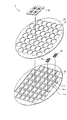
- FIG. 1 is a perspective view showing the configuration of the inspection system according to the first embodiment of the present invention.
- FIG. 2 is an exploded perspective view showing the configuration of the inspection system according to the first embodiment of the present invention.
- FIG. 3 is a perspective view showing a configuration of a main part of the inspection system shown in FIGS.
- FIG. 4 is a perspective view showing a configuration of a main part of the inspection system shown in FIGS.
- FIG. 5 is a perspective view showing a configuration of a main part of the inspection system shown in FIGS.
- FIG. 6 is a perspective view showing a configuration of a main part of the inspection system shown in FIGS.
- FIG. 7 is a partial cross-sectional view illustrating a configuration of a main part of the inspection system according to the first embodiment of the present invention.
- FIG. 8 is a cross-sectional view illustrating a configuration of a main part of the inspection system according to the first embodiment of the present invention.
- FIG. 9 is a cross-sectional view illustrating a configuration of a main part of the inspection system according to the first embodiment of the present invention.
- FIG. 10 is a partial cross-sectional view showing another configuration of the main part of the inspection system according to the first embodiment of the present invention.
- FIG. 11 is a perspective view showing the configuration of the inspection system according to the second embodiment of the present invention.
- FIG. 12 is an exploded perspective view showing the configuration of the inspection system according to the second embodiment of the present invention.
- FIG. 13 is a perspective view showing a configuration of a main part of the inspection system shown in FIGS. FIG.
- FIG. 14 is a cross-sectional view showing a configuration of a main part of the inspection system shown in FIGS.
- FIG. 15 is a perspective view showing a configuration of a main part of the inspection system shown in FIGS.
- FIG. 16 is a perspective view showing a configuration of a main part of the inspection system shown in FIGS.
- FIG. 17 is a perspective view showing a configuration of a main part of the inspection system shown in FIGS.
- FIG. 18 is a perspective view showing a configuration of a main part of the inspection system shown in FIGS.
- FIG. 19 is a partial cross-sectional view illustrating a configuration of a main part of the inspection system according to the second embodiment of the present invention.
- FIG. 15 is a perspective view showing a configuration of a main part of the inspection system shown in FIGS.
- FIG. 16 is a perspective view showing a configuration of a main part of the inspection system shown in FIGS.
- FIG. 17 is a perspective view showing a configuration of a main part
- FIG. 20 is a cross-sectional view illustrating a configuration of a main part of the inspection system according to the second embodiment of the present invention.
- FIG. 21 is a cross-sectional view illustrating a configuration of a main part of the inspection system according to the second embodiment of the present invention.
- FIG. 1 is a perspective view showing the configuration of the inspection system according to the first embodiment.
- FIG. 2 is an exploded perspective view showing the configuration of the inspection system according to the first embodiment.
- An inspection system 1 shown in FIGS. 1 and 2 is an apparatus used when performing an electrical characteristic inspection on a semiconductor package 20 to be inspected, and includes a semiconductor package 20 and a circuit board that outputs an inspection signal to the semiconductor package 20. It is an apparatus for electrically connecting between.
- the inspection system 1 includes a substantially disc-shaped tray 10 that holds a substantially rectangular semiconductor package 20, and a substantially disc-shaped lid 30 that can contact at least an end of the semiconductor package 20 held on the tray 10. And a probe unit 40 for electrically connecting the semiconductor package 20 and the circuit board.
- the tray 10 has a holding hole 11 that is formed on the main surface 10 a of the tray 10 and can hold the semiconductor package 20. Further, the holding hole 11 is formed with an insertion hole 11a through which a pin 43 as a positioning means described later can be inserted. Here, at least two insertion holes 11 a are formed for each holding hole 11. When two insertion holes 11 a are formed with respect to the holding hole 11, the insertion holes 11 a are formed at positions corresponding to two continuous sides of the held semiconductor package 20.
- the tray 10 is formed by using a material that can cope with the inspection temperature. Moreover, even when the semiconductor package to be inspected is expanded by using a material having the same or similar linear expansion coefficient as that of the semiconductor package, accurate positioning can be performed.
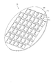
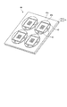
- the semiconductor package 20 is a BGA (Ball Grid Array), and solder balls 21 as electrodes are arranged in a substantially rectangular shape on the surface 20a as shown in the perspective view of FIG.
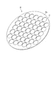
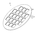
- the lid 30 covers the tray 10 in substantially the same outer edge shape as the tray 10, and has a circular opening 31 provided corresponding to the holding hole 11 as shown in the perspective view of FIG.
- the opening 31 is circular with a diameter slightly smaller than the diagonal length of the semiconductor package 20.
- the probe unit 40 includes a conductive contact probe 50 (hereinafter simply referred to as a “probe 50”) that contacts two different contacted semiconductor packages 20 and a circuit board, and a plurality of probes 50 according to a predetermined pattern. And a probe holder 41 as a holding portion that accommodates and holds.
- a probe unit that can be contacted simultaneously with four semiconductor packages will be described as an example.
- the probe holder 41 is formed by laminating a first member 41a located on the lower surface side in FIG. 6 and a second member 41b located on the upper surface side.
- the first member 41 a and the second member 41 b are formed with the same number of first holder holes 42 a and second holder holes 42 b (holder holes 42) for receiving the plurality of probes 50, respectively.
- the first holder hole 42a and the second holder hole 42b are formed so that their axes coincide with each other.
- the probe holder 41 has a pin 43 that projects from a surface 40 a facing the lid 30 and has a tapered tip shape that is inserted into the insertion hole 11 a of the tray 10. 6 shows a perspective view in which the probe unit 40 shown in FIGS.
- a columnar protrusion 40b that can be inserted into the opening 31 of the lid 30 is formed on the surface 40a of the probe unit 40 on the side that contacts the lid 30.
- the arrangement of the probe 50 is the same as that of the semiconductor package 20.
- the holder holes 42 are arranged so as to have the same arrangement as the pattern.
- a plurality of protrusions 40b are formed on the surface 40a of the probe unit corresponding to the arrangement of the openings 31.
- the holder hole 42 includes a first holder hole 42a and a second holder hole 42b, both of which have a stepped hole shape with different diameters along the penetration direction. That is, the first holder hole 42a includes a small diameter portion 42c having an opening at the upper end surface of the probe holder 41 and a large diameter portion 42d having a diameter larger than that of the small diameter portion 42c.
- the 2nd holder hole 42b consists of the small diameter part 42e which has an opening in the lower end surface of the probe holder 41, and the large diameter part 42f whose diameter is larger than this small diameter part 42e.
- the shapes of the first holder hole 42a and the second holder hole 42b are determined according to the configuration of the probe 50 to be accommodated. Thereby, it has the function to prevent the probe 50 from being removed from the probe holder 41.
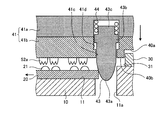
- the probe 50 shown in FIG. 7 is formed using a conductive material, and a first plunger 51 that contacts an electrode on the circuit board side, and a second plunger 52 that contacts the solder ball 21 when the semiconductor package 20 is inspected. And a spring member 53 that is provided between the first plunger 51 and the second plunger 52 and connects the two first plungers 51 and the second plunger 52 in a telescopic manner.
- the first plunger 51 and the second plunger 52 and the spring member 53 constituting the probe 50 have the same axis.
- the first plunger 51 has a distal end portion 51a having a tapered distal end shape that contacts the electrode on the circuit board side, a flange portion 51b having a diameter larger than the diameter of the distal end portion 51a, and a distal end via the flange portion 51b. It has a base end portion 51c that extends to the opposite side of the portion 51a, has a smaller diameter than the flange portion 51b, and into which the end of the spring member 53 is press-fitted.
- the second plunger 52 is opposed to the tip portion 52a having a plurality of claw portions having a tapered tip shape, the flange portion 52b having a diameter larger than the diameter of the tip portion 52a, and the tip portion 52a of the flange portion 52b. And a base end portion 52c into which the end portion of the spring member 53 is press-fitted.
- the spring member 53 has a tightly wound portion 53a on the first plunger 51 side and a coarsely wound portion 53b on the second plunger 52 side.
- the end portion of the tightly wound portion 53a is press-fitted into the proximal end portion 51c and is in contact with the flange portion 51b.
- the end portion of the coarsely wound portion 53b is press-fitted into the base end portion 52c and is in contact with the flange portion 52b.
- the spring member 53 is elastically deformed in the connecting direction with the semiconductor package 20.
- the spring member 53 When the semiconductor package 20 is inspected, the spring member 53 is compressed along the longitudinal direction due to the contact load from the semiconductor package 20. When the spring member 53 is compressed, the tightly wound portion 53 a comes into contact with the proximal end portion 52 d of the second plunger 52. Thereby, reliable electrical conduction is obtained.
- the pin 43 is held in a first holding hole 41c and a second holding hole 41d formed in the probe holder 41.
- the pin 43 has a substantially columnar shape and is connected to a tip portion 43a having a tapered tip, a flange portion 43b having a diameter larger than the maximum diameter of the tip portion 43a, and a flange portion. And a boss portion 43c having a diameter smaller than that of the flange portion 43b.
- the diameter of the first holding hole 41c is smaller than the diameter of the second holding hole 41d.
- the flange 43b contacts the stepped shape formed by the first holding hole 41c and the second holding hole 41d, thereby preventing the pin 43 from being detached from the probe holder 41.
- the pin 43 has a boss portion 43c press-fitted into a coil-shaped spring member 44 having one end fixed to the bottom surface of the second holding hole 41d. As a result, the pin 43 can move forward and backward in the direction of insertion into the insertion hole 11a.
- the pin 43 may be provided with a spring member between the end surface of the flange portion 43b and the bottom surface of the second holding hole 41d without providing the boss portion 43c.
- the pins 43 are inserted while being guided along the wall surface of the insertion hole 11 a of the tray 10 (FIG. 8). At this time, the side surface of the pin 43 is in contact with the end portion of the semiconductor package 20 and applies a force to the semiconductor package 20. With this force, the semiconductor package 20 moves to the wall surface facing the insertion hole 11 a of the holding hole 11. Further, as shown in FIG. 6, the pin 43 is provided corresponding to the insertion hole 11 a provided on the two adjacent sides on the rectangular outer edge (four sides), and therefore, one of the four corners of the holding hole 11 is provided. The semiconductor package 20 is moved to the corner.
- a plurality of pins for positioning the semiconductor package on the probe unit side and a plurality of insertion holes into which the pins can be inserted are provided in the tray holding the semiconductor package, and the tray and the probe unit are brought close to each other.
- the positioning of the plurality of semiconductor packages on the tray and the contact with the electrodes of the semiconductor package are performed at the same time, so that it is possible to accurately inspect the inspection object that has been cut into pieces with a simple configuration.
- the semiconductor package can be transported. Can be ensured. Furthermore, by adjusting the size of the tray with respect to the cassette for storing the wafer, it can be used for a wafer inspection apparatus.
- the configuration of the first embodiment requires only a positioning pin on the probe unit side and an insertion hole for inserting the pin on the tray side. Therefore, accurate inspection and shortening of the inspection time can be achieved with a simple configuration. In addition, it is possible to cope with this by simply providing an insertion hole in the current tray.
- the pin 43 may be made of metal, may be made of resin, or may cover the base material made of metal with resin.
- the pin 43 can be designed depending on the material of the semiconductor package 20 or the like.
- the semiconductor package to be used is applicable to PGA (Pin Grid Array) etc. other than BGA mentioned above.
- the probe may be a pogo pin 54 as shown in FIG.
- the pogo pin 54 shown in FIG. 10 is held by a probe holder 41c having a stepped shape at one end side of the holder hole, and has tip portions 54a and 54b that can be advanced and retracted in one longitudinal direction at both ends.
- the tip portions 54a and 54b make electrical connection between the circuit board and the semiconductor package by making contact with the circuit board and the semiconductor package, respectively.
- FIG. 11 is a perspective view showing the configuration of the inspection system according to the second embodiment.
- FIG. 12 is an exploded perspective view showing the configuration of the inspection system according to the second embodiment.
- An inspection system 2 shown in FIGS. 11 and 12 is an apparatus used when an electrical characteristic inspection is performed on a semiconductor package 70 to be inspected, and includes a semiconductor package 70 and a circuit board that outputs an inspection signal to the semiconductor package 70. It is an apparatus for electrically connecting between.
- the inspection system 2 includes a substantially disc-shaped tray 60 that holds a substantially rectangular semiconductor package 70 and a substantially disc-shaped lid that can come into contact with a part of the main surface of the semiconductor package 70 held by the tray 60. And a probe unit 90 for electrically connecting the semiconductor package 70 and the circuit board.
- the tray 60 has a holding hole 61 that is formed on the main surface 60 a of the tray 60 and can hold the semiconductor package 70.
- the holding hole 61 is provided in communication with the first holding hole 61a having a substantially rectangular opening for holding the semiconductor package 70 and the opening surface of the first holding hole 61a.
- a second holding hole 61b having a substantially rectangular opening larger than the first holding hole 61a.
- the arrangement heights of the first holding hole 61a and the second holding hole 61b correspond to the protruding height of the lead 71 and the height of the tip of the semiconductor package 70 described later.
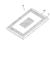
- the semiconductor package 70 is a rectangular QFP (Quad Flat Package), and as shown in a perspective view of FIG. 15, leads 71 as electrodes protrude from a surface orthogonal to the main surface 70a. Has been.
- the lead 71 protrudes from a surface orthogonal to the main surface 70 a and has a bent shape so that the height (extending height) of the tip portion is the same as the upper surface of the semiconductor package 70.
- the lid 80 has substantially the same outer edge shape as the tray 60 and covers the tray 60, and has an opening 81 provided corresponding to the holding hole 61 as shown in the perspective view of FIG.
- the opening 81 includes a first opening 81 a having a circular shape with a smaller diameter than the main surface 70 a of the semiconductor package 70 and four second openings 81 b formed corresponding to the shape of the outer edge of the holding hole 61.
- the opening 81 abuts against the end of the semiconductor package 70 even when the tray 60 is inverted to prevent the semiconductor package 70 from being detached from the holding hole 61. can do.
- the lid 80 contacts the probe unit 90 on the surface 80a side. Further, the tray 60 and the lid 80 are fixed by screwing or fitting.
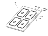
- the probe unit 90 includes a conductive contact probe 100 (hereinafter simply referred to as “probe 100”) that contacts two different contact objects, ie, a semiconductor package 70 and a circuit board, and a plurality of probes 100 according to a predetermined pattern. And a probe holder 91 as a holding portion for receiving and holding. As shown in FIGS. 17 and 18, the probe holder 91 has a protrusion 90 b provided on the surface 90 a corresponding to the lead 71 of each semiconductor package 70 and the second opening 81 b of the lid 80. Yes. A holder hole 92 for holding the contact probe 100 is formed in a surface parallel to the surface 90a of the protruding portion 90b. On the surface 90 a, the four protruding portions 90 b have a rectangular shape corresponding to one semiconductor package 70.
- the probe holder 91 is formed by laminating a first member 91a located on the lower surface side in FIG. 17 and a second member 91b located on the upper surface side.
- the first member 91a and the second member 91b are formed with the same number of first holder holes 92a and second holder holes 92b (holder holes 92) for receiving the plurality of probes 100, respectively.
- the first holder hole 92a and the second holder hole 92b are formed so that their axes coincide with each other.
- the probe holder 91 has a leaf spring 93 as a positioning means that is provided on the surface 90 a on the side facing the lid 80 and can contact the main surface of the semiconductor package 70.
- FIG. 17 shows a perspective view in which the probe unit 90 shown in FIGS. 11 and 12 is inverted.
- a protrusion 90b having a substantially columnar shape that can be inserted into the second opening 81b of the lid 80 is formed on the surface 90a of the probe unit 90 that contacts the lid 80, and the lead of one semiconductor package 70 is formed.
- the holder holes 92 are arranged so as to have the same arrangement as the arrangement pattern 71.
- a plurality of protrusions 90b are formed on the surface 90a of the probe unit corresponding to the arrangement of the second openings 81b.
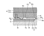
- the holder hole 92 is composed of a first holder hole 92a and a second holder hole 92b as shown in the partial cross-sectional view shown in FIG. 19, and has a stepped hole shape with different diameters along the penetration direction. That is, the first holder hole 92a includes a small-diameter portion 92c having an opening on the upper end surface of the probe holder 91 and a large-diameter portion 92d having a larger diameter than the small-diameter portion 92c.
- the second holder hole 92b includes a small diameter portion 92e having an opening at the lower end surface of the probe holder 91 and a large diameter portion 92f having a diameter larger than the small diameter portion 92e.
- the shapes of the first holder hole 92a and the second holder hole 92b are determined according to the configuration of the probe 100 to be accommodated. Thereby, it has a function of preventing the probe 100 from being removed from the probe holder 91.
- the leaf spring 93 is fixed to the surface 90a by a screw 93a and extends so as to rise in an oblique direction from the surface 90a. Further, as shown in FIGS. 17 and 18, the leaf spring 93 is fixed to at least the second member 91b by a screw 93a. As shown in FIG. 18, the leaf spring 93 is provided so as to extend toward any corner (vertex) of the outer edge (four sides) formed by the protruding portion 90 b, and the four corners of the first holding hole 61 a. The semiconductor package 70 is moved toward one corner.
- the leaf spring 93 may be made of metal, may be made of resin, or may cover the surface of the metal base material with resin. Further, it is preferable that at least a portion of the leaf spring 93 that contacts the semiconductor package 70 has a high frictional force.
- a probe 100 shown in FIG. 19 is formed using a conductive material, and is connected to the first plunger 101 having the same configuration as the first plunger 51 shown in FIG. 7 and the lead 71 when the semiconductor integrated circuit 70 is inspected.
- a second plunger 102 that is in contact with each other, and a spring member 103 that is provided between the first plunger 101 and the second plunger 102 and that connects the two first plungers 101 and the second plunger 102 so as to expand and contract.
- the first plunger 101 and the second plunger 102 and the spring member 103 constituting the probe 100 have the same axis.
- the first plunger 101 has a distal end portion 101a, a flange portion 101b, and a proximal end portion 101c, similarly to the distal end portion 51a, the flange portion 51b, and the proximal end portion 51c shown in FIG.
- the second plunger 102 is opposed to the tip portion 102a having a tapered tip shape contacting the lead 71, a flange portion 102b having a diameter larger than the diameter of the tip portion 102a, and the tip portion 102a of the flange portion 102b. And a base end portion 102c having a diameter smaller than that of the flange portion 102b and into which the end portion of the spring member 103 is press-fitted.
- the spring member 103 has a tightly wound portion 103a on the first plunger 101 side, and a coarsely wound portion 103b on the second plunger 102 side.
- the end of the tightly wound portion 103a is press-fitted into the base end portion 101c and is in contact with the flange portion 101b.
- the end of the coarsely wound portion 103b is press-fitted into the base end portion 102c and is in contact with the flange portion 102b.
- the spring member 103 is elastically deformed in the connection direction with the semiconductor package 70.
- the spring member 103 When the semiconductor package 70 is inspected, the spring member 103 is compressed along the longitudinal direction due to the contact load from the semiconductor package 70. When the spring member 103 is compressed, the tightly wound portion 103 a comes into contact with the proximal end portion 102 d of the second plunger 102.
- the leaf spring 93 comes into contact with the semiconductor package 70, and a force is applied to the semiconductor package 70, so that the semiconductor package 70 is attached to the leaf spring 93. It is moved in the extending direction (right direction in FIG. 20). At this time, the leaf spring 93 contacts the main surface 70 a of the semiconductor package 70 and moves the semiconductor package 70. With this force, the semiconductor package 70 moves to the boundary wall surface side between the first holding hole 61a and the second holding hole 61b.
- the pins for positioning the semiconductor package on the probe unit side and the tray for holding the semiconductor package are used. Since a plurality of insertion holes into which pins can be inserted are provided, and the tray and the probe unit are brought close to each other, positioning of a plurality of semiconductor packages on the tray and contact with the electrodes of the semiconductor package are performed simultaneously. With the configuration, it is possible to accurately inspect the inspection target that has been cut into pieces, and to reduce the time required for the inspection of the inspection target that has been cut into pieces.
- positioning may be performed using the pins of the inspection system according to the first embodiment described above.
- the pins are disposed at positions where two or more of the four corners of each semiconductor package 70 can be abutted, and the semiconductor package 70 is moved to the remaining corners to be positioned. It is more preferable that pins are arranged at positions where they can come into contact with the three corners of the semiconductor package 70.
- the probe unit has been described as corresponding to four semiconductor packages. However, any probe unit can be used as long as it can contact two or more semiconductor packages. It may be possible to contact the semiconductor package at the same time.
- the inspection system and the package holder according to the present invention are useful for conducting electrical continuity by connecting a plurality of pieces of electric circuit boards cut into pieces with a simple configuration.
Landscapes
- Engineering & Computer Science (AREA)
- Computer Hardware Design (AREA)
- Microelectronics & Electronic Packaging (AREA)
- General Engineering & Computer Science (AREA)
- Physics & Mathematics (AREA)
- General Physics & Mathematics (AREA)
- Testing Of Individual Semiconductor Devices (AREA)
- Measuring Leads Or Probes (AREA)
- Packaging Frangible Articles (AREA)
Abstract
Description
図1は、本実施の形態1にかかる検査システムの構成を示す斜視図である。図2は、本実施の形態1にかかる検査システムの構成を示す分解斜視図である。図1,2に示す検査システム1は、検査対象である半導体パッケージ20の電気特性検査を行う際に使用する装置であって、半導体パッケージ20と半導体パッケージ20へ検査用信号を出力する回路基板との間を電気的に接続するための装置である。
図11は、本実施の形態2にかかる検査システムの構成を示す斜視図である。図12は、本実施の形態2にかかる検査システムの構成を示す分解斜視図である。図11,12に示す検査システム2は、検査対象である半導体パッケージ70の電気特性検査を行う際に使用する装置であって、半導体パッケージ70と半導体パッケージ70へ検査用信号を出力する回路基板との間を電気的に接続するための装置である。
10,60 トレイ
11,61 保持穴
11a 挿入孔
20,70 半導体パッケージ
21 半田ボール
30,80 蓋体
31,81 開口部
40,90 プローブユニット
41,91 プローブホルダ
42,92 ホルダ孔
43 ピン
50,100 プローブ
61a 第1保持穴
61b 第2保持穴
71 リード
81a 第1開口部
81b 第2開口部
93 板バネ
Claims (6)
- 検査対象のパッケージを保持する保持穴を複数有するトレイと、
検査を行う際に前記パッケージの電極と接続するコンタクトプローブと、
前記コンタクトプローブを保持するプローブホルダと、
前記プローブホルダに設けられ、前記検査を行う際に前記保持穴に対する前記パッケージの位置決めを行う位置決め手段と、
を備えたことを特徴とする検査システム。 - 前記トレイの上面を覆い、前記パッケージが有する電極を外部に露出する開口部を有し、前記トレイによって保持されたパッケージの少なくとも一部と当接可能な蓋体をさらに備えたことを特徴とする請求項1に記載の検査システム。
- 前記位置決め手段は、前記プローブホルダから該プローブホルダの主面に垂直な方向に延びる先細な先端形状をなす複数のピンであって、
前記トレイは、前記ピンの先端が挿入可能な挿入孔を有し、
前記ピンは、前記検査を行う際に、前記パッケージの外縁に当接して前記パッケージを所定位置に移動させることを特徴とする請求項1または2に記載の検査システム。 - 前記ピンは、前記プローブホルダの主面に垂直な方向に進退可能であることを特徴とする請求項3に記載の検査システム。
- 前記位置決め手段は、検査を行う際に前記パッケージの主面に当接して前記パッケージを前記保持穴の所定位置に移動させる板バネであって、
前記板バネは、前記プローブホルダの主面から前記所定位置に向けて斜めの方向に立ち上がって延在することを特徴とする請求項1または2に記載の検査システム。 - 検査対象のパッケージを保持する保持穴を複数有するトレイと、
前記トレイの上面を覆い、前記パッケージが有する電極を外部に露出する開口部を有し、前記トレイによって保持されたパッケージの少なくとも一部と当接可能な蓋体と、
を備えたことを特徴とするパッケージ保持具。
Priority Applications (3)
| Application Number | Priority Date | Filing Date | Title |
|---|---|---|---|
| JP2012549838A JP6039425B2 (ja) | 2010-12-22 | 2011-12-20 | 検査システム |
| PH1/2013/501331A PH12013501331A1 (en) | 2010-12-22 | 2011-12-20 | Test system and package holder |
| SG2013048301A SG191306A1 (en) | 2010-12-22 | 2011-12-20 | Test system and package holder |
Applications Claiming Priority (2)
| Application Number | Priority Date | Filing Date | Title |
|---|---|---|---|
| JP2010-286689 | 2010-12-22 | ||
| JP2010286689 | 2010-12-22 |
Publications (1)
| Publication Number | Publication Date |
|---|---|
| WO2012086653A1 true WO2012086653A1 (ja) | 2012-06-28 |
Family
ID=46313921
Family Applications (1)
| Application Number | Title | Priority Date | Filing Date |
|---|---|---|---|
| PCT/JP2011/079551 Ceased WO2012086653A1 (ja) | 2010-12-22 | 2011-12-20 | 検査システムおよびパッケージ保持具 |
Country Status (5)
| Country | Link |
|---|---|
| JP (1) | JP6039425B2 (ja) |
| PH (1) | PH12013501331A1 (ja) |
| SG (2) | SG191306A1 (ja) |
| TW (1) | TWI460445B (ja) |
| WO (1) | WO2012086653A1 (ja) |
Cited By (2)
| Publication number | Priority date | Publication date | Assignee | Title |
|---|---|---|---|---|
| JP2015087269A (ja) * | 2013-10-31 | 2015-05-07 | 三菱電機株式会社 | 半導体評価装置および半導体評価方法 |
| TWI748705B (zh) * | 2020-10-23 | 2021-12-01 | 美商第一檢測有限公司 | 晶片托盤套件及晶片測試設備 |
Citations (4)
| Publication number | Priority date | Publication date | Assignee | Title |
|---|---|---|---|---|
| JPS62151744U (ja) * | 1986-03-19 | 1987-09-26 | ||
| JPH07140190A (ja) * | 1993-11-15 | 1995-06-02 | Nec Kyushu Ltd | 電気的特性試験実施可能なic搬送用トレーおよびそれを用いた電気的特性試験の方法 |
| JP2004296155A (ja) * | 2003-03-26 | 2004-10-21 | Enplas Corp | 電気部品用ソケット |
| JP2010243314A (ja) * | 2009-04-06 | 2010-10-28 | Syswave Corp | 半導体チップ素子試験治具及び自動試験装置 |
Family Cites Families (5)
| Publication number | Priority date | Publication date | Assignee | Title |
|---|---|---|---|---|
| JP2004063268A (ja) * | 2002-07-29 | 2004-02-26 | Yamaichi Electronics Co Ltd | Lga用icソケット |
| JP2006284384A (ja) * | 2005-03-31 | 2006-10-19 | Fujitsu Ltd | 半導体装置の試験装置及び試験方法 |
| JP5243037B2 (ja) * | 2006-10-27 | 2013-07-24 | 株式会社アドバンテスト | 電子部品試験装置 |
| WO2009144790A1 (ja) * | 2008-05-28 | 2009-12-03 | 株式会社アドバンテスト | 電子部品ハンドリング装置、電子部品試験装置および電子部品保持トレイ |
| TWI402517B (zh) * | 2010-02-24 | 2013-07-21 | Fugu Tech Entpr Co Ltd | 檢測系統及檢測方法 |
-
2011
- 2011-12-20 WO PCT/JP2011/079551 patent/WO2012086653A1/ja not_active Ceased
- 2011-12-20 JP JP2012549838A patent/JP6039425B2/ja not_active Expired - Fee Related
- 2011-12-20 SG SG2013048301A patent/SG191306A1/en unknown
- 2011-12-20 PH PH1/2013/501331A patent/PH12013501331A1/en unknown
- 2011-12-20 SG SG10201510500XA patent/SG10201510500XA/en unknown
- 2011-12-22 TW TW100147921A patent/TWI460445B/zh not_active IP Right Cessation
Patent Citations (4)
| Publication number | Priority date | Publication date | Assignee | Title |
|---|---|---|---|---|
| JPS62151744U (ja) * | 1986-03-19 | 1987-09-26 | ||
| JPH07140190A (ja) * | 1993-11-15 | 1995-06-02 | Nec Kyushu Ltd | 電気的特性試験実施可能なic搬送用トレーおよびそれを用いた電気的特性試験の方法 |
| JP2004296155A (ja) * | 2003-03-26 | 2004-10-21 | Enplas Corp | 電気部品用ソケット |
| JP2010243314A (ja) * | 2009-04-06 | 2010-10-28 | Syswave Corp | 半導体チップ素子試験治具及び自動試験装置 |
Cited By (3)
| Publication number | Priority date | Publication date | Assignee | Title |
|---|---|---|---|---|
| JP2015087269A (ja) * | 2013-10-31 | 2015-05-07 | 三菱電機株式会社 | 半導体評価装置および半導体評価方法 |
| US9678143B2 (en) | 2013-10-31 | 2017-06-13 | Mitsubishi Electric Corporation | Semiconductor evaluation apparatus |
| TWI748705B (zh) * | 2020-10-23 | 2021-12-01 | 美商第一檢測有限公司 | 晶片托盤套件及晶片測試設備 |
Also Published As
| Publication number | Publication date |
|---|---|
| JP6039425B2 (ja) | 2016-12-07 |
| JPWO2012086653A1 (ja) | 2014-05-22 |
| TWI460445B (zh) | 2014-11-11 |
| SG10201510500XA (en) | 2016-01-28 |
| TW201237440A (en) | 2012-09-16 |
| SG191306A1 (en) | 2013-08-30 |
| PH12013501331A1 (en) | 2022-10-24 |
Similar Documents
| Publication | Publication Date | Title |
|---|---|---|
| KR101535229B1 (ko) | 범용 테스트 소켓 및 이를 이용한 반도체 패키지 테스트 장치 | |
| JP5982372B2 (ja) | 接触構造体ユニット | |
| KR20100076853A (ko) | 반도체 장치용 전기 접속 장치 및 그것에 사용되는 콘택트 | |
| JP2006269404A (ja) | 電子部品用コンタクタ及びコンタクト方法 | |
| US20240361352A1 (en) | Test socket and assembly device thereof | |
| JP2023153760A (ja) | テストソケット用コンタクトピンおよびこれを含むテストソケット | |
| JP4911495B2 (ja) | 半導体集積回路用ソケット | |
| JP6039425B2 (ja) | 検査システム | |
| JP7148017B2 (ja) | 検査治具及びそれを備えた基板検査装置 | |
| JP5865846B2 (ja) | 検査ソケット | |
| JP7301582B2 (ja) | 電気的接触子及び電気的接続装置 | |
| KR100466483B1 (ko) | 집적회로패키지용소켓장치 | |
| JP2011180019A (ja) | 半導体測定装置および半導体測定装置用ピッチ変換治具 | |
| TWI917929B (zh) | 測試插座及其組裝裝置 | |
| CN223007009U (zh) | 顺应性探针接触组件及具有其的测试系统 | |
| JP2014154265A (ja) | ソケット本体及びicソケット | |
| JP2001235514A (ja) | 電気検査治具,検査ピン及び電気検査機の使用方法 | |
| JP7536263B2 (ja) | カバーソケット、ハンドリング装置及び半導体検査書き込み装置 | |
| JP2000258493A (ja) | 半導体素子検査装置 | |
| JP2004340599A (ja) | 検査用ソケット | |
| JP2005308453A (ja) | 測定装置 | |
| JP2007205995A (ja) | 高周波プローブ | |
| JP2000292487A (ja) | デバイスキャリア及び水平搬送式オートハンドラ | |
| KR200421330Y1 (ko) | 전자회로 검사장치 | |
| KR100647494B1 (ko) | 전자회로 검사장치 및 그 검사방법 |
Legal Events
| Date | Code | Title | Description |
|---|---|---|---|
| 121 | Ep: the epo has been informed by wipo that ep was designated in this application |
Ref document number: 11851799 Country of ref document: EP Kind code of ref document: A1 |
|
| ENP | Entry into the national phase |
Ref document number: 2012549838 Country of ref document: JP Kind code of ref document: A |
|
| WWE | Wipo information: entry into national phase |
Ref document number: 12013501331 Country of ref document: PH |
|
| NENP | Non-entry into the national phase |
Ref country code: DE |
|
| 122 | Ep: pct application non-entry in european phase |
Ref document number: 11851799 Country of ref document: EP Kind code of ref document: A1 |