WO2012086411A1 - ワイヤレス電力伝送システム、送電装置および受電装置 - Google Patents
ワイヤレス電力伝送システム、送電装置および受電装置 Download PDFInfo
- Publication number
- WO2012086411A1 WO2012086411A1 PCT/JP2011/078242 JP2011078242W WO2012086411A1 WO 2012086411 A1 WO2012086411 A1 WO 2012086411A1 JP 2011078242 W JP2011078242 W JP 2011078242W WO 2012086411 A1 WO2012086411 A1 WO 2012086411A1
- Authority
- WO
- WIPO (PCT)
- Prior art keywords
- electrode
- power transmission
- power
- power receiving
- active electrode
- Prior art date
- Legal status (The legal status is an assumption and is not a legal conclusion. Google has not performed a legal analysis and makes no representation as to the accuracy of the status listed.)
- Ceased
Links
Images








Classifications
-
- H—ELECTRICITY
- H02—GENERATION; CONVERSION OR DISTRIBUTION OF ELECTRIC POWER
- H02J—ELECTRIC POWER NETWORKS; CIRCUIT ARRANGEMENTS OR SYSTEMS FOR SUPPLYING OR DISTRIBUTING ELECTRIC POWER; SYSTEMS FOR STORING ELECTRIC ENERGY
- H02J50/00—Circuit arrangements or systems for wireless supply or distribution of electric power
- H02J50/70—Circuit arrangements or systems for wireless supply or distribution of electric power involving the reduction of electric, magnetic or electromagnetic leakage fields
-
- H—ELECTRICITY
- H02—GENERATION; CONVERSION OR DISTRIBUTION OF ELECTRIC POWER
- H02J—ELECTRIC POWER NETWORKS; CIRCUIT ARRANGEMENTS OR SYSTEMS FOR SUPPLYING OR DISTRIBUTING ELECTRIC POWER; SYSTEMS FOR STORING ELECTRIC ENERGY
- H02J50/00—Circuit arrangements or systems for wireless supply or distribution of electric power
- H02J50/05—Circuit arrangements or systems for wireless supply or distribution of electric power using capacitive coupling
-
- H—ELECTRICITY
- H02—GENERATION; CONVERSION OR DISTRIBUTION OF ELECTRIC POWER
- H02J—ELECTRIC POWER NETWORKS; CIRCUIT ARRANGEMENTS OR SYSTEMS FOR SUPPLYING OR DISTRIBUTING ELECTRIC POWER; SYSTEMS FOR STORING ELECTRIC ENERGY
- H02J7/00—Circuit arrangements for charging or discharging batteries or for supplying loads from batteries
- H02J7/70—Circuit arrangements for charging or discharging batteries or for supplying loads from batteries characterised by the mechanical construction
-
- H—ELECTRICITY
- H02—GENERATION; CONVERSION OR DISTRIBUTION OF ELECTRIC POWER
- H02J—ELECTRIC POWER NETWORKS; CIRCUIT ARRANGEMENTS OR SYSTEMS FOR SUPPLYING OR DISTRIBUTING ELECTRIC POWER; SYSTEMS FOR STORING ELECTRIC ENERGY
- H02J7/00—Circuit arrangements for charging or discharging batteries or for supplying loads from batteries
- H02J7/70—Circuit arrangements for charging or discharging batteries or for supplying loads from batteries characterised by the mechanical construction
- H02J7/731—Circuit arrangements for charging or discharging batteries or for supplying loads from batteries characterised by the mechanical construction specially adapted for holding portable devices containing batteries
Definitions
- the present invention relates to a wireless power transmission system, a power transmission device, and a power reception device that transmit power from a power transmission device to a power reception device mounted on the power transmission device.
- a magnetic field coupling type power transmission system in which power is transmitted from a primary coil of a power transmission apparatus to a secondary coil of a power reception apparatus using a magnetic field.
- this system when electric power is transmitted by magnetic coupling, since the magnitude of magnetic flux passing through each coil greatly affects the electromotive force, high accuracy is required for the relative positional relationship between the primary coil and the secondary coil. Moreover, since the coil is used, it is difficult to reduce the size of the apparatus.
- Patent Document 1 an electric field coupling type wireless power transmission system as disclosed in Patent Document 1 is also known.
- power is transmitted from the coupling electrode of the power transmission apparatus to the coupling electrode of the power reception apparatus via an electric field.
- the required relative positional accuracy of the coupling electrode is relatively loose, and the coupling electrode can be reduced in size and thickness.
- FIG. 1 is a diagram showing a basic configuration of a power transmission system described in Patent Document 1.
- This power transmission system includes a power transmission device and a power reception device.
- the power transmission device includes a high frequency high voltage generation circuit 1, a passive electrode 2, and an active electrode 3.
- the power receiving device includes a high frequency high voltage load circuit 5, a passive electrode 7, and an active electrode 6. Then, when the active electrode 3 of the power transmission device and the active electrode 6 of the power reception device come close to each other through the gap 4, the two electrodes are electrically coupled to form a strong electric field between the electrodes, thereby achieving high transmission. Efficient power transmission is possible.
- the power receiving device examples include electronic devices such as a mobile phone and a PDA (Personal Digital Assistant). Recently, a capacitive input unit (touch panel) with good operability is used for these electronic devices. A lot is happening. In this case, the power receiving device may be placed on the power transmitting device and the touch panel may be operated while being charged. However, as described above, the power receiving device is caused by the electric field formed on the active electrode of the power transmitting device and the power receiving device. The potential may fluctuate and the touch panel may malfunction.
- electronic devices such as a mobile phone and a PDA (Personal Digital Assistant).
- a capacitive input unit (touch panel) with good operability is used for these electronic devices. A lot is happening.
- the power receiving device may be placed on the power transmitting device and the touch panel may be operated while being charged.
- the power receiving device is caused by the electric field formed on the active electrode of the power transmitting device and the power receiving device. The potential may fluctuate and the touch panel may malfunction.
- an object of the present invention is to provide a wireless power transmission system, a power transmission device, and a power reception device that stabilize the potential of the power transmission device and the power reception device during power transmission from the power transmission device to the power reception device and do not cause malfunction of the power reception device. There is to do.
- an object of the present invention is to provide a wireless power transmission system, a power transmission device, and a power reception device that stabilize the potential of the power transmission device and the power reception device during power transmission from the power transmission device to the power reception device and do not cause malfunction of the power reception device. There is to do.
- a wireless power transmission system includes a power transmission device including a power transmission side electrode and a voltage generation circuit that applies a voltage to the power transmission side electrode, a power reception side electrode that is capacitively coupled to the power transmission side electrode, and the power reception side
- a wireless power transmission system comprising: a step-down circuit that steps down a voltage generated at an electrode; and a power receiving device that includes a load circuit that inputs an output voltage of the step-down circuit as a power supply voltage.
- the power transmitting device or the power receiving device includes: An electrostatic shielding unit that electrostatically shields the power transmission side electrode and the power reception side electrode with respect to the ground is provided.
- the electrode is electrostatically shielded from the ground.
- the ground potential of the power transmission device and the power reception device may vary from the ground potential. Due to the influence, there is a risk that the touch panel or the like that operates based on the ground potential becomes inoperable or the display on the display is disturbed. For this reason, when the capacitively coupled electrode is not electrostatically shielded, a stray capacitance is formed between the electrode and the ground.
- the power transmission side electrode has a power transmission side active electrode and a power transmission side passive electrode having a lower potential than the power transmission side active electrode
- the power reception side electrode is a power reception side active electrode
- a power-receiving-side passive electrode having a lower potential than the power-receiving-side active electrode, the power-transmission-side active electrode and the power-receiving-side active electrode facing each other through a gap
- the power-transmission-side passive electrode and the power-receiving The side passive electrode may be configured to face or contact via a gap.
- the ground potential of the power transmitting device and the power receiving device can be further stabilized by electrostatically shielding the active electrode serving as the high voltage portion with respect to the ground, thereby further preventing malfunction of the power transmitting device or the power receiving device. it can.
- the power transmission side electrode has a power transmission side first electrode and a power transmission side second electrode, and the power reception side electrode is opposite to the power transmission side first electrode.
- a power receiving side second electrode facing the power transmitting side second electrode the voltage generating circuit applies voltages having opposite phases to the power transmitting side first electrode and the power transmitting side second electrode,
- the step-down circuit may be configured to step down the output voltage from the power receiving side first electrode and the power receiving side second electrode.
- the four electrodes having high voltage can be electrostatically shielded from the ground.
- the electrostatic shielding unit electrostatically shields the voltage generation circuit from the ground.
- the electrostatic shielding unit electrostatically shields the step-down circuit from the ground.
- the power receiving device may include a capacitance type input unit that uses a potential of the power receiving side passive electrode as a reference potential.
- an input operation is detected by detecting that a ground connection is made via a human body (a minute current flows) by touching the capacitive input unit of the power receiving device. For this reason, by stabilizing the ground potential of the power transmitting device and the power receiving device during power transmission, even when the capacitance type input unit (touch panel) is operated during power transmission, the capacitance type input unit Since the ground connection due to touching can be reliably detected, malfunction of the power receiving device during operation of the touch panel can be reduced.
- the electrostatic shielding unit may be the power transmission side passive electrode or the power reception side passive electrode.
- the power receiving device has a front surface on which the capacitive input unit is provided, a back surface parallel to the front surface, and a bottom surface adjacent to the front surface and the back surface,
- the power-receiving-side active electrode is provided along the bottom surface
- the power-receiving-side passive electrode is provided along the back surface
- the power transmitting device is a mounting surface on which the bottom surface of the power receiving device is in surface contact, and the back surface of the power receiving device A backrest surface in surface contact, and a front surface facing the backrest surface across the placement surface
- the power transmission side active electrode is provided along the placement surface
- the power transmission side passive electrode is Provided along a backrest surface and the front surface, and provided on the opposite side of the mounting surface across the power transmission side active electrode, the power transmission side active electrode on the mounting surface described above Provided I, the power transmission side passive electrode, said back surface and the provided along the front surface, and may be configured on the opposite side to the mounting surface across the transmitting side active
- the power transmission side and power reception side active electrodes can be electrostatically shielded by the power transmission side passive electrodes.
- the power receiving device has a front surface on which the capacitive input unit is provided, a back surface parallel to the front surface, and a bottom surface adjacent to the front surface and the back surface,
- the power receiving side active electrode is provided along the back surface
- the power receiving side passive electrode is a bottom surface side passive electrode provided along the bottom surface, and the back side facing the back surface across the power receiving side active electrode
- the power transmission device has a mounting surface on which the bottom surface of the power receiving device is in surface contact and a backrest surface on which the back surface of the power receiving device is in surface contact, and the power transmission side active electrode is on the back surface.
- the power transmission side passive electrode is sandwiched between the mounting surface side passive electrode provided along the mounting surface and the power transmission side active electrode. It may be configured with a backrest surface active electrode opposed to serial backplate surface.
- the power transmission side and power reception side active electrodes can be electrostatically shielded by the power transmission side passive electrodes.
- the power receiving device has a front surface on which the capacitive input unit is provided, a back surface parallel to the front surface, and a bottom surface adjacent to the front surface and the back surface,
- the power-receiving-side first electrode and the power-receiving-side second electrode of the power-receiving-side active electrode are provided along the bottom surface or the back surface
- the power transmitting device is a mounting surface on which the bottom surface of the power receiving device is in surface contact
- the power receiving device has a backrest surface in contact with the back surface, and the power transmission side first electrode and the power transmission side second electrode of the power transmission side active electrode are provided along the mounting surface or the backrest surface. It may be configured.
- the power transmission side and power reception side active electrodes can be electrostatically shielded by the power transmission side passive electrodes.
- an electrode that is capacitively coupled by an electrostatic shielding unit is electrostatically shielded with respect to the ground, so that the power transmission device and the power receiving device have a ground potential that varies from the ground potential during power transmission. Can be prevented from malfunctioning.
- FIG. 3 is a perspective view of the power transmission device and the power reception device of the wireless power transmission system according to the first embodiment.
- the schematic circuit diagram of a power receiving apparatus The figure which simplified the equivalent circuit of FIG. Schematic diagram of an equivalent circuit of a wireless power transmission system when the reference potential of the power receiving device includes an electrostatic shielding electrode
- FIG. 8 is an equivalent circuit diagram of the wireless power transmission system shown in FIG. 7.
- FIG. 1 The side view of the power transmission apparatus and power receiving apparatus of the wireless power transmission system which concern on Embodiment 2.
- FIG. The figure which shows the wireless power transmission system which concerns on Embodiment 3.
- FIG. The perspective view of a power transmission apparatus and a power receiving apparatus.
- the schematic diagram which shows another example of the structure which the passive electrode of a power transmission apparatus shields an active electrode electrostatically.
- the schematic diagram which shows another example of the structure which the passive electrode of a power transmission apparatus shields an active electrode electrostatically.
- the schematic diagram which shows another example of the structure which the passive electrode of a power transmission apparatus shields an active electrode electrostatically.
- FIG. 16 is a side cross-sectional view of a power transmission device and a power reception device, which is a modification of the wireless power transmission system illustrated in FIG. 15.
- FIG. 6 is an equivalent circuit diagram of a wireless power transmission system according to the fourth embodiment.
- the wireless power transmission system according to the present invention includes a power transmission device and a power reception device.
- the power receiving device is, for example, a portable electronic device including a secondary battery. Examples of portable electronic devices include a mobile phone, a PDA (Personal Digital Assistant), a portable music player, a notebook PC (Personal Computer), and a digital camera.
- the power transmission device is a charging stand on which the power reception device is mounted and charges a secondary battery of the power reception device.
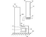
- FIG. 2 is a perspective view of the power transmission device and the power reception device of the wireless power transmission system according to the first embodiment.
- the power receiving apparatus 201 includes a substantially rectangular parallelepiped casing 20 having a secondary battery (not shown) therein.
- a capacitance type input unit hereinafter referred to as a touch panel 23 along the front surface.
- the touch panel 23 is an input unit of the power receiving device 201. That is, the touch panel 23 is an input unit that operates the power receiving apparatus 201 by combining a display function and a position input function and pressing a display on the screen.
- the casing 20 is provided with a rectangular active electrode 21 and a passive electrode 22 along the longitudinal direction of the back surface (hereinafter referred to as the height direction of the power receiving device 201).
- the active electrode 21 faces an active electrode 11 (described later) provided on the power transmission apparatus 101 via a gap
- the passive electrode 22 is provided on the power transmission apparatus 101. It faces the passive electrode 12 via a gap. Part or all of the passive electrode 22 may be exposed so as to be directly connected to the passive electrode 12 on the power transmission apparatus 101 side.
- the power transmission device 101 includes a housing 10 having an L shape in a side view.
- the housing 10 has a mounting surface 10A that is substantially horizontal to the installation surface (earth) and a backrest surface 10B that is substantially perpendicular to the mounting surface 10A and faces each other in parallel.
- the placement surface 10A and the backrest surface 10B are each rectangular.
- the power receiving apparatus 201 is mounted on the power transmitting apparatus 101 such that the bottom surface of the power receiving apparatus 201 is on the mounting surface 10A side and the back surface of the power receiving apparatus 201 is on the backrest surface 10B side.
- the casing 10 is provided with a rectangular active electrode 11 and a passive electrode 12 along the longitudinal direction of the backrest surface 10B (hereinafter referred to as the height direction of the power receiving device 201).
- the active electrodes 11 and 21 face each other with a gap therebetween
- the passive electrodes 12 and 22 face each other with a gap therebetween.
- the power transmission device 101 includes an electrostatic shielding electrode 13 provided along the mounting surface 10A.
- the electrostatic shielding electrode 13 is connected to a ground potential (ground potential) that is a reference potential of the power transmission device 101.
- the electrostatic shielding electrode 13 has a rectangular shape, and the active electrodes 11 and 21 and the passive electrodes 12 and 22 that face each other during power transmission are provided on the upper side in the height direction of the power transmission device 101. In other words, the electrostatic shielding electrode 13 is interposed between the opposed active electrodes 11 and 21 and the passive electrodes 12 and 22 and the ground (ground, floor, desk, etc.).
- the power receiving device 201 is placed on the power transmitting device 101, the passive electrodes 12 and 22 are opposed, and the active electrodes 11 and 21 are opposed. Then, a voltage is applied by a voltage generation circuit (not shown) to generate an electric field between the active electrodes 11 and 21 that are arranged to face each other, and power is transmitted from the power transmitting apparatus 101 to the power receiving apparatus 201 via this electric field. . Thereby, the secondary battery of the power receiving apparatus 201 is charged.
- the touch panel 23 of the power receiving apparatus 201 can be operated during the power transmission operation.
- the touch panel 23 may be erroneously operated. May cause operation.
- malfunctioning of the touch panel 23 can be prevented by electrostatically shielding the active electrodes 11 and 21, which are high-voltage portions, with respect to the ground (ground, floor, desk, etc.) by the electrostatic shielding electrode 13.
- FIG. 3 is a schematic diagram of an equivalent circuit of the wireless power transmission system when the power receiving apparatus 201 is mounted on the power transmitting apparatus 101.
- the power transmission device 101 includes an AC adapter 16 and a voltage generation circuit 17.
- the AC adapter 16 rectifies 100V AC voltage, converts it to DC voltage such as 5V, 12V, etc., and outputs it to the voltage generation circuit 17.
- the voltage generation circuit 17 includes an inverter 18, a step-up transformer TG, and an inductor LG.
- the voltage generation circuit 17 performs AC conversion and step-up on the voltage input from the AC adapter 16 and applies the voltage between the active electrode 11 and the passive electrode 12.
- the frequency of the applied voltage is 100 kHz to 10 MHz.
- a step-down circuit 25 using a step-down transformer TL and an inductor LL is connected.
- a load circuit RL and a touch panel 23 are connected to the secondary side of the step-down transformer TL.
- the load circuit RL includes a rectifying / smoothing circuit and a secondary battery (not shown).
- the touch panel 23 uses the secondary battery of the load circuit RL as a driving power source.
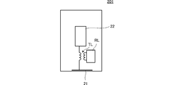
- FIG. 4 is a schematic circuit diagram of the power receiving apparatus 201.
- the primary side of the step-down transformer TL is connected between the passive electrode 22 and the active electrode 21.
- a load circuit RL is connected to the secondary side of the step-down transformer TL.
- the touch panel 23 is omitted.
- the active electrode 11 and the active electrode 21 come close to each other through a gap, and constitute a capacitor Ca. Further, the passive electrode 12 and the passive electrode 22 also form a capacitor Cp in close proximity via a gap.
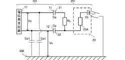
- FIG. 5 is a simplified diagram of the equivalent circuit of FIG.
- the touch panel 23 is a capacitance detection system, and by touching the touch panel 23, a capacitance (capacitor Ct) is formed between the human body and the touch panel 23, and the touch panel 23 is grounded via the human body. It becomes. A weak current flows through the capacitor Ct, and an input position on the touch panel 23 is detected by detecting a change in the current with the detector 23A.
- the power transmission device 101 and the power reception device 201 are isolated from the ground 300, and therefore, as shown by the dotted line in FIG.
- a stray capacitance Ca1 is configured between the electrode 11 and the ground 300
- a stray capacitance Cp1 is configured between the passive electrode 12 and the ground 300.
- the output voltage from the voltage generation circuit 17 is divided by the stray capacitance Ca1 and the stray capacitance Cp1. Specifically, when the output voltage Vo of the voltage generation circuit 17 and the voltage Vn of the stray capacitance Cp1 are set, the voltage Vn is Vo * Ca1 / (Ca1 + Cp1).
- the touch panel 23 operates using the ground potential (that is, the voltage Vn) of the power receiving apparatus 201 as the reference potential. Therefore, if the reference potential (voltage Vn) varies, the touch panel 23 is normal. Will not work. For this reason, it is necessary to reduce the variation of the reference potential (voltage Vn) of the touch panel 23 as much as possible. Therefore, if the stray capacitance Ca1 is made as small as possible (smaller than the stray capacitance Cp1), the voltage Vn can be reduced accordingly, and the ground potential (voltage Vn) of the power transmitting device 101 and the power receiving device 201 during power transmission can be stabilized. .
- the high voltage portion such as the active electrode 11 is electrostatically shielded from the ground 300 by the electrostatic shielding electrode 13.
- the stray capacitance Ca1 shown in FIG. 5 can be made smaller than the stray capacitance Cp1, and the divided voltage Vn by the stray capacitances Ca1 and Cp1 can be suppressed.
- the fluctuation of the ground potential with respect to the ground can be suppressed. Accordingly, even if the touch panel 23 of the power receiving apparatus 201 is touched during the power transmission operation, the touch panel 23 does not malfunction.
- the electrostatic shielding electrode 13 is connected to the reference potential of the power transmission device 101.
- the electrostatic shielding electrode 13 may be connected to the reference potential of the power receiving device 201.
- FIG. 6 is a schematic diagram of an equivalent circuit of the wireless power transmission system when the reference potential of the power receiving apparatus 201 includes the electrostatic shielding electrode 13.
- the electrostatic shielding electrode 13 is provided in the power transmission device 101, and the electrostatic shielding electrode 13 is connected to the reference potential of the power reception device 201 when the power reception device 201 is placed on the power transmission device 101.
- the touch panel 23 operates with this reference potential as a reference.
- the stray capacitance Ca1 shown in FIG. 5 can be made smaller than the stray capacitance Cp1, and the divided voltage Vn by the stray capacitances Ca1 and Cp1 can be suppressed. Can be suppressed.
- malfunction of the power receiving apparatus 201 when the touch panel 23 is touched during the power transmission operation of the power receiving apparatus 201 can be prevented.
- the passive electrodes 12 and 22 of the power transmitting apparatus 101 and the power receiving apparatus 201 are opposed to each other via a gap.
- the passive electrodes 12 and 22 may be directly connected.
- the passive electrodes 12 and 22 may be directly conducted by exposing a part of the passive electrodes 12 and 22 from the housings 10 and 20.
- FIG. 7 is a simplified circuit diagram of a wireless power transmission system in which passive electrodes are directly connected to each other.
- a high frequency high voltage generation circuit OSC is connected between the active electrode 11 and the passive electrode 12.
- a step-down circuit 25 is connected between the active electrode 21 and the passive electrode 22, and a load circuit RL is connected to the step-down circuit 25.
- the passive electrodes 12 and 22 do not need to have the flat plate shape described with reference to FIG.
- the high frequency high voltage generation circuit OSC applies a high frequency high voltage between the power transmission device side active electrode 11 and the power transmission device side passive electrode 12.
- the step-down circuit 25 steps down a voltage generated between the power receiving device side active electrode 21 and the power receiving device side passive electrode 22.
- the load circuit RL inputs the output voltage of the step-down circuit 25 as a power supply voltage.
- the load circuit RL includes a rectifying / smoothing circuit that rectifies and smoothes the output of the step-down circuit 25 and a secondary battery that is charged by the output of the rectifying and smoothing circuit.
- the power receiving device side passive electrode 22 is in direct contact with the power transmitting device side passive electrode 12 in a direct current manner.
- the current flowing through the power transmitting device side passive electrode 12 may be, for example, on the order of several mA.
- a charging current of the order of several A flows as it is, so that loss due to contact resistance is large.
- various contact means such as conductive rubber can be applied.
- FIG. 8 is an equivalent circuit diagram of the wireless power transmission system shown in FIG.
- the high frequency high voltage generation circuit OSC of the power transmission apparatus 101 generates a high frequency voltage of 100 kHz to several tens of MHz, for example.
- the step-up transformer 19 using the step-up transformer TG and the inductor LG steps up the voltage generated by the high-frequency high-voltage generation circuit OSC and applies it between the active electrode 11 and the passive electrode 12.
- a step-down circuit 25 including a step-down transformer TL and an inductor LL is connected between the power receiving device-side active electrode 21 and the power receiving device-side passive electrode 22.
- a load circuit RL is connected to the secondary side of the step-down transformer TL.
- the load circuit RL includes a rectifying / smoothing circuit and a secondary battery.
- the resistance r connected between the power transmission device side passive electrode 12 and the power reception device side passive electrode 22 corresponds to a contact resistance configured at a contact portion between the power transmission device side passive electrode 12 and the power reception device side passive electrode 22.
- a capacitance Ca is generated between the power transmitting device side active electrode 11 and the power receiving device side active electrode 21.
- the contact resistance r and the capacitance Ca of the capacitive coupling portion have a relationship of r ⁇ 1 / ⁇ Ca.
- the passive electrodes of the power transmission device 101 and the power reception device 201 are directly connected to each other, so that the potential of the power reception device side passive electrode 12 becomes substantially equal to the potential of the power transmission device side passive electrode 22.
- the potential of the power receiving apparatus side passive electrode 22 is stabilized, and ground potential fluctuations and leakage of unnecessary electromagnetic fields are suppressed.
- stray capacitance is suppressed, the degree of coupling increases and high transmission efficiency is obtained.
- FIG. 9 is a side view of a power transmission device and a power reception device of the wireless power transmission system according to the second embodiment.
- Members and the like included in the power transmitting apparatus 101 and the power receiving apparatus 201 according to the present embodiment are the same as those in the first embodiment.
- the active electrode 11 of the power transmission apparatus 101 is provided along the mounting surface 10A.
- the passive electrode 12 is provided in parallel to the placement surface 10A so that the active electrode 11 is interposed between the passive electrode 12 and the placement surface 10A.
- the electrostatic shielding electrode 13 is provided between the active electrode 11 and the passive electrode 12 and the ground 300.
- the active electrode 21 of the power receiving apparatus 201 is provided along the bottom surface.
- the passive electrode 22 is provided in parallel to the bottom surface so that the active electrode 21 is interposed between the passive electrode 22 and the bottom surface.
- the active electrodes 11 and 21 and the passive electrodes 12 and 22 are electrically coupled to each other through a gap during power transmission.
- power is transmitted from the power transmitting apparatus 101 to the power receiving apparatus 201.
- the electrostatic shielding electrode 13 is interposed between the active electrodes 11 and 21 serving as the high voltage portion and the ground 300, the high voltage portion is electrostatically shielded from the ground (ground, floor, desk, etc.). be able to.
- the touch panel 23 is operated during the power transmission operation, the presence or absence of the operation of the touch panel 23 can be reliably detected, and the malfunction of the touch panel 23 can be suppressed.
- FIG. 10 is a diagram illustrating a wireless power transmission system according to the third embodiment.
- Members and the like included in the power transmitting apparatus 101 and the power receiving apparatus 201 according to the present embodiment are the same as those in the first embodiment.
- the housing 10 of the power transmission apparatus 101 is different from the first and second embodiments.
- the casing 10 of the power transmission apparatus 101 has a front surface 10C that is substantially perpendicular to the placement surface 10A and faces the backrest surface 10B in parallel.
- the mounting surface 10A, the backrest surface 10B, and the front surface 10C each have a rectangular shape.
- the long side of the mounting surface 10A matches the short side of the backrest surface 10B, and the long side of the mounting surface 10A matches the long side of the front surface 10C.
- the front surface 10 ⁇ / b> C has a size that does not overlap with the touch panel 23 provided on the front surface of the housing 20 when the power receiving device 201 is placed.
- the active electrode 11 of the power transmission apparatus 101 is provided along the backrest surface 10B.
- the passive electrode 12 is provided in parallel to the backrest surface 10B so that the active electrode 11 is interposed between the passive electrode 12 and the backrest surface 10B.
- the electrostatic shielding electrode 13 includes a placement surface 10A and a backrest surface 10B so as to surround the active electrodes 11 and 21 and the passive electrodes 12 and 22 that face each other when the power receiving device 201 is placed on the placement surface 10A.
- the front surface 10C The power transmission device 101 includes the electrostatic shielding electrode 13 in which the surfaces along the placement surface 10A, the backrest surface 10B, and the front surface 10C are integrated, but the static electricity electrode formed independently for each surface. An electric shielding electrode may be provided.
- the active electrode 21 of the power receiving apparatus 201 is provided along the back surface.
- the passive electrode 22 is provided in parallel to the back surface so that the active electrode 21 is interposed between the passive electrode 22 and the back surface.
- the active electrodes 11 and 21 and the passive electrodes 12 and 22 are electrically coupled to each other through a gap during power transmission.
- power is transmitted from the power transmitting apparatus 101 to the power receiving apparatus 201.
- the electrostatic shielding electrode 13 is interposed between the active electrodes 11 and 21 serving as the high voltage portion and the ground 300, the high voltage portion is electrostatically shielded from the ground (ground, floor, desk, etc.). be able to.
- the touch panel 23 is operated during the power transmission operation, the presence or absence of the operation of the touch panel 23 can be reliably detected, and the malfunction of the power receiving apparatus 201 can be suppressed.
- Embodiment 4 of the present invention will be described below.
- the electrostatic shielding electrode for electrostatic shielding with respect to the ground is provided as an independent member, but in the fourth embodiment, the passive electrode is used as the electrostatic shielding electrode.
- FIG. 11 is a perspective view of the power transmitting device and the power receiving device.
- FIG. 12 is a side view of the power transmission device and the power reception device. Note that the casing 10 of the power transmission device 101 according to the present embodiment has the same shape as that of the third embodiment.
- the passive electrode 22 is provided on the casing 20 of the power receiving apparatus 201 along the back surface.
- the passive electrode 22 has a rectangular shape and is provided so that the longitudinal direction thereof coincides with the height direction of the power receiving device 201.
- the passive electrode 22 faces a passive electrode 121 (described later) provided on the power transmission apparatus 101 via a gap. Part or all of the passive electrode 22 may be exposed so as to be directly connected to the passive electrode 121 on the power transmission device 101 side.
- the housing 20 of the power receiving apparatus 201 is provided with an active electrode 21 along the bottom surface.
- the bottom surface of the housing 20 has a rectangular shape, and its long side coincides with the short sides of the front surface and the back surface.
- the active electrode 21 has a rectangular shape and is provided so that the longitudinal direction thereof coincides with the longitudinal direction of the bottom surface of the housing 20 (hereinafter referred to as the width direction of the power receiving device 201).
- the active electrode 21 is opposed to the later-described active electrode 11 provided in the power transmission device 101 via a gap.
- the housing 10 of the power transmission apparatus 101 has a placement surface 10A, a backrest surface 10B, and a front surface 10C, as in the third embodiment.
- the mounting surface 10A, the backrest surface 10B, and the front surface 10C each have a rectangular shape.
- the long side of the mounting surface 10A matches the short side of the backrest surface 10B, and the long side of the mounting surface 10A matches the long side of the front surface 10C.
- the power receiving apparatus 201 is mounted on the power transmitting apparatus 101 such that the bottom surface of the power receiving apparatus 201 is on the mounting surface 10A side and the back surface of the power receiving apparatus 201 is on the backrest surface 10B side.
- the front surface 10 ⁇ / b> C has a size that does not overlap with the touch panel 23 provided on the front surface of the housing 20 when the power receiving device 201 is placed.
- the power transmission device 101 includes an active electrode 11 provided along the mounting surface 10A.
- the active electrode 11 has a rectangular shape and is provided such that its longitudinal direction coincides with the longitudinal direction of the placement surface 10A (hereinafter referred to as the width direction of the power transmission device 101).
- the active electrode 11 on the power transmitting apparatus 101 side and the active electrode 21 on the power receiving apparatus 201 side face each other with a gap therebetween.
- the casing 10 is provided with passive electrodes 121 along the backrest surface 10B.
- the passive electrode 121 has a rectangular shape and is provided such that the longitudinal direction thereof coincides with the height direction of the power transmission device 101.
- the passive electrode 121 on the power transmitting apparatus 101 side and the passive electrode 22 on the power receiving apparatus 201 side face each other (or directly conduct).
- the housing 10 is provided perpendicular to the passive electrode 121, and further provided with passive electrodes 122 and 123 so as to face the mounting surface 10A in parallel.
- the passive electrodes 122 and 123 have a rectangular shape and are provided such that the longitudinal direction thereof coincides with the width direction of the power transmission apparatus 101.
- the passive electrode 122 is provided between the active electrode 11 and the passive electrode 123 in the height direction of the power transmission device 101.
- the power transmission device 101 includes a passive electrode 124 provided along the front surface 10C.
- the passive electrode 124 is provided orthogonal to the passive electrodes 122 and 123 and parallel to the passive electrode 121.
- Passive electrodes 121, 122, and 124 surround three surfaces of active electrode 11 of power transmission device 101.
- the active electrode 11 on the power transmitting apparatus 101 side and the active electrode 21 on the power receiving apparatus 201 side that face each other are surrounded by the passive electrodes 121, 122, and 124.
- the power transmission device 101 includes a voltage generation circuit 17 that applies AC conversion and boosting of a DC voltage supplied via an AC adapter to be applied between the active electrode 11 and the passive electrode 121.
- the voltage generation circuit 17 is provided between the passive electrode 122 and the passive electrode 123. Accordingly, the four sides of the voltage generation circuit 17 are surrounded by the passive electrodes 121, 122, 123, and 124.
- the power transmission device 101 surrounds the high-voltage portions such as the active electrodes 11 and 21 and the voltage generation circuit 17 that are electrically coupled with the passive electrodes 121, 122, 123, and 124, thereby grounding the high-voltage portions (ground). , Floor, desk, etc.).
- the circuit configuration of the wireless power transmission system according to the fourth embodiment is the same as that of the first to third embodiments except that the electrostatic shielding electrode 13 is not provided.
- the active electrodes 11 and 21 that face each other when the power receiving apparatus 201 is placed on the power transmitting apparatus 101 are grounded by the passive electrodes 121, 122, 123, and 124.
- it is set as the structure which carries out electrostatic shielding. Thereby, the ground potential of the power transmission apparatus 101 and the power reception apparatus 201 can be stabilized.
- the power reception apparatus 201 causes a malfunction. I can not.
- the passive electrode 22 on the power receiving device 201 side is provided only on the back surface of the housing 20, a passive electrode may be further provided along the side surface of the housing 20.
- the active electrode of the power transmission apparatus 101 and the power receiving apparatus 201 is provided on the mounting surface 10A of the power transmission apparatus 101 and the bottom surface of the housing 20, it is not limited thereto.
- FIGS. 13, 14 and 15 are schematic views showing another example of a configuration in which the passive electrode of the power transmission apparatus 101 electrostatically shields the active electrode.
- the active electrode 11 is provided along the backrest surface 10 ⁇ / b> B of the power transmission device 101
- the active electrode 21 is provided along the back surface of the housing 20 of the power reception device 201.
- the passive electrodes 125 and 22 of the power transmission apparatus 101 and the power reception apparatus 201 are provided so as to face each other with the active electrodes 11 and 21 interposed therebetween.
- the passive electrode 24 is provided along the bottom surface of the housing 20, and the passive electrode 126 facing the passive electrode 24 is provided along the mounting surface 10 ⁇ / b> A of the power transmission device 101.
- the opposed active electrodes 11 and 21 are electrostatically shielded from the ground by the passive electrodes 125, 126, 22, and 24.
- the active electrode 11 and the passive electrode 12 are provided along the placement surface 10 ⁇ / b> A of the power transmission device 101, and the active electrode 21 and the passive electrode 22 are provided along the bottom surface of the power reception device 201. May be.
- opposed active electrodes 11 and 21 are interposed between the opposed passive electrodes 12 and 22.
- the passive electrode 12 functions as an electrostatic shielding part with respect to the ground.
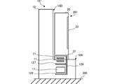
- the voltage generation circuit 17 of the power transmission device 101 that is a high voltage portion may be surrounded by passive electrodes 127, 128, and 129.
- the active electrode 11 and the passive electrode 127 of the power transmission device 101 are provided along the placement surface 10 ⁇ / b> A of the housing 10.
- a passive electrode 129 is provided so that the voltage generation circuit 17 is interposed between the passive electrode 127 and the passive electrodes 127 and 129 are electrically connected by the passive electrode 128.
- the active electrode 21 and the passive electrode 22 of the power receiving device 201 are provided along the bottom surface of the housing 20.
- the voltage generation circuit 17 can also be electrostatically shielded from the ground 300 by the passive electrodes 127, 128, and 129 that function as electrostatic shielding electrodes.
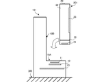
- FIG. 16 is a modification of the wireless power transmission system shown in FIG. 15, and is a side cross-sectional view of the power transmission apparatus 101 and the power reception apparatus 201.
- the passive electrode 128 is formed so that a part is exposed from the mounting surface 10 ⁇ / b> A of the housing 10. Further, the passive electrode 22 of the power receiving device 201 is formed so as to be partially exposed from the bottom surface of the housing 20.
- the passive electrode 129 that functions as an electrostatic shielding electrode for the voltage generation circuit 17 is set to the same potential as the passive electrode 22 of the power receiving device 201. Even with this configuration, the high voltage portion can be electrostatically shielded from the ground 300, and malfunction of the touch panel 23 can be prevented.
- Each of the power transmitting device and the power receiving device according to the fifth embodiment includes a pair of active electrodes.
- FIG. 17 is a perspective view of the power transmitting device and the power receiving device.
- FIG. 18 is a side view of the power transmission device and the power reception device. Note that the casing 10 of the power transmission device 101 according to the present embodiment has the same shape as the third and fourth embodiments.
- Active electrode 111,112 is provided in the housing
- the active electrodes 111 and 112 have a rectangular shape and are arranged in the height direction of the power transmission device 101.
- the electrostatic shielding electrode 131 is provided in parallel to the backrest surface 10B.
- the electrostatic shielding electrode 132 is provided along the mounting surface 10 ⁇ / b> A of the housing 10.
- the electrostatic shielding electrode 132 is disposed so as to be interposed between a high voltage portion such as a voltage generation circuit (not shown) and the ground 300.
- the electrostatic shielding electrode 133 is provided along the front surface 10 ⁇ / b> C of the housing 10.
- the housing 20 of the power receiving apparatus 201 is provided with active electrodes 211 and 212 along the back surface.
- the active electrodes 211 and 212 have a rectangular shape and are arranged in the height direction of the power receiving apparatus 201.
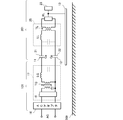
- FIG. 19 is an equivalent circuit diagram of the wireless power transmission system according to this embodiment.
- one end of the secondary winding of the transformer TG is connected to the active electrode 111 and the other end is connected to the active electrode 112.
- one end of the primary winding of the step-down transformer TL is connected to the active electrode 211, and the other end is connected to the active electrode 212.
- the secondary winding of the step-down transformer TL is connected to the load circuit RL via diodes D1 and D2 at both ends.
- the secondary winding has a center tap, and the center tap is connected to the load circuit RL.
- the active electrode 111 and the active electrode 211 that face each other, and the electrostatic shielding electrodes 131, 132, and 133 are provided between the opposing active electrode 112 and the active electrode 212 and the ground 300.
- Each electrode is electrostatically shielded from the ground 300.
- the active electrodes 111 and 112 are provided along the backrest surface 10B of the housing 10, but may be provided along the placement surface 10A. In this case, the active electrodes 211 and 212 are provided along the bottom surface of the housing 20. Further, on the secondary side of the step-down transformer TL of the power receiving device 201, the rectifier circuit is configured by two diodes D1 and D2, but may be a diode bridge circuit or another configuration.
Landscapes
- Engineering & Computer Science (AREA)
- Power Engineering (AREA)
- Computer Networks & Wireless Communication (AREA)
- Physics & Mathematics (AREA)
- Electromagnetism (AREA)
- Charge And Discharge Circuits For Batteries Or The Like (AREA)
- Near-Field Transmission Systems (AREA)
Abstract
Description
図2は、実施形態1に係るワイヤレス電力伝送システムの送電装置と受電装置との透視斜視図である。
次に、実施形態2に係るワイヤレス電力伝送システムについて説明する。本実施形態では、送電装置101および受電装置201におけるアクティブ電極およびパッシブ電極の配置が実施形態1と相違する。送電装置101および受電装置201の回路構成は、実施形態1と同様であり、説明は省略する。
次に、実施形態3に係るワイヤレス電力伝送システムについて説明する。本実施形態では、送電装置101および受電装置201におけるアクティブ電極およびパッシブ電極の配置が実施形態1と相違する。
以下に、本発明の実施形態4について説明する。実施形態1~3では、アースに対して静電遮蔽する静電遮蔽電極を独立した部材として設けているが、実施形態4では、パッシブ電極を静電遮蔽電極として用いている。
以下に、本発明に係る実施形態5について説明する。実施形態5に係る送電装置および受電装置のぞれぞれは、一対のアクティブ電極を備えている。
10A-載置面
10B-背もたれ面
10C-前面
11-アクティブ電極
12-パッシブ電極
13-静電遮蔽電極
17-電圧発生回路
20-筐体
21-アクティブ電極
22-パッシブ電極
23-タッチパネル
101-送電装置
201-受電装置
300-アース
RL-負荷回路
Claims (14)
- 送電側電極と、前記送電側電極に電圧を印加する電圧発生回路とを備える送電装置と、
前記送電側電極に対し容量結合する受電側電極、前記受電側電極に発生する電圧を降圧する降圧回路、および前記降圧回路の出力電圧を電源電圧として入力する負荷回路を有する受電装置と、
を備えるワイヤレス電力伝送システムにおいて、
前記送電装置または前記受電装置は、
前記送電側電極および前記受電側電極をアースに対して静電遮蔽する静電遮蔽部
を備えるワイヤレス電力伝送システム。 - 前記送電側電極は送電側アクティブ電極および、前記送電側アクティブ電極より低電位となる送電側パッシブ電極を有し、
前記受電側電極は受電側アクティブ電極および、前記受電側アクティブ電極より低電位となる受電側パッシブ電極を有し、
前記送電側アクティブ電極および前記受電側アクティブ電極は、間隙を介して対向して容量結合し、
前記送電側パッシブ電極および前記受電側パッシブ電極は、間隙を介して対向または接触する、
請求項1に記載のワイヤレス電力伝送システム。 - 前記送電側電極は送電側第1電極および送電側第2電極を有し、
前記受電側電極は、前記送電側第1電極に対向する受電側第1電極、および前記送電側第2電極に対向する受電側第2電極を有し、
前記電圧発生回路は、前記送電側第1電極および前記送電側第2電極に互いに逆位相となる電圧を印加し、
前記降圧回路は、前記受電側第1電極および受電側第2電極からの出力電圧を降圧する、
請求項1に記載のワイヤレス電力伝送システム。 - 前記静電遮蔽部は前記電圧発生回路を前記アースに対して静電遮蔽する、
請求項1から3の何れかに記載のワイヤレス電力伝送システム。 - 前記静電遮蔽部は前記降圧回路を前記アースに対して静電遮蔽する、
請求項1から4の何れかに記載のワイヤレス電力伝送システム。 - 前記受電装置は、前記受電側パッシブ電極の電位を基準電位とする静電容量式入力部を有する、
請求項2から5の何れかに記載のワイヤレス電力伝送システム。 - 前記静電遮蔽部は前記送電側パッシブ電極または前記受電側パッシブ電極である、
請求項1から6の何れかに記載のワイヤレス電力伝送システム。 - 前記受電装置は、
前記静電容量式入力部が設けられる前面、前記前面と平行な背面、並びに、前記前面および前記背面に隣接する底面を有し、
前記受電側アクティブ電極は前記底面に沿って設けられ、
前記受電側パッシブ電極は前記背面に沿って設けられ、
前記送電装置は、
前記受電装置の底面が面接触する載置面、前記受電装置の背面が面接触する背もたれ面、および前記載置面を挟んで前記背もたれ面と対向する前面を有し、
前記送電側アクティブ電極は前記載置面に沿って設けられ、
前記送電側パッシブ電極は、前記背もたれ面および前記前面に沿って設けられ、かつ、前記送電側アクティブ電極を挟んで載置面とは反対側に設けられ、
前記送電側アクティブ電極は前記載置面に沿って設けられ、
前記送電側パッシブ電極は、前記背もたれ面および前記前面に沿って設けられ、かつ、前記送電側アクティブ電極を挟んで載置面とは反対側に設けられた、
請求項7に記載のワイヤレス電力伝送システム。 - 前記受電装置は、
前記静電容量式入力部が設けられる前面、前記前面と平行な背面、並びに、前記前面および前記背面に隣接する底面を有し、
前記受電側アクティブ電極は前記背面に沿って設けられ、
前記受電側パッシブ電極は、前記底面に沿って設けられた底面側パッシブ電極、および、前記受電側アクティブ電極を挟んで前記背面に対向する背面側パッシブ電極を有し、
前記送電装置は、
前記受電装置の底面が面接触する載置面、および前記受電装置の背面が面接触する背もたれ面を有し、
前記送電側アクティブ電極は前記背もたれ面に沿って設けられ、
前記送電側パッシブ電極は、前記載置面に沿って設けられた載置面側パッシブ電極、および前記送電側アクティブ電極を挟んで前記背もたれ面に対向する背もたれ面側アクティブ電極を有する、
請求項7に記載のワイヤレス電力伝送システム。 - 前記受電装置は、
前記静電容量式入力部が設けられる前面、前記前面と平行な背面、並びに、前記前面および前記背面に隣接する底面を有し、
前記受電側アクティブ電極の前記受電側第1電極および前記受電側第2電極は前記底面または前記背面に沿って設けられ、
前記送電装置は、
前記受電装置の底面が面接触する載置面、および前記受電装置の背面が面接触する背もたれ面を有し、
前記送電側アクティブ電極の前記送電側第1電極および前記送電側第2電極は、前記載置面または前記背もたれ面に沿って設けられている、
請求項7に記載のワイヤレス電力伝送システム。 - 受電側アクティブ電極、受電側パッシブ電極、前記受電側アクティブ電極および送電側パッシブ電極の間に生じる電圧を降圧する降圧回路、並びに、前記降圧回路の出力電圧を電源電圧として入力する負荷回路を有する受電装置が載置され、該受電装置へ電力を送電する送電装置において、
載置される前記受電装置の受電側アクティブ電極が間隙を介して対向する送電側アクティブ電極と、
載置される前記受電装置の受電側パッシブ電極が対向または接触する送電側パッシブ電極と、
前記送電側アクティブ電極および送電側パッシブ電極間に電圧を印加する電圧発生回路と、
前記送電側アクティブ電極、または載置される前記受電装置の受電側アクティブ電極の少なくとも一方をアースに対して静電遮蔽する静電遮蔽部と、
を備える送電装置。 - 前記送電側アクティブ電極は送電側第1電極および送電側第2電極を有し、
前記電圧発生回路は、
前記送電側第1電極および前記送電側第2電極に互いに逆位相となる電圧を印加する、
請求項11に記載の送電装置。 - 送電側アクティブ電極、送電側パッシブ電極、並びに、前記送電側アクティブ電極及び送電側パッシブ電極間に電圧を印加する電圧発生回路を有する送電装置へ載置して、該送電装置から電力が受電する受電装置において、
前記送電装置の送電側アクティブ電極に空隙を介して対向する受電側アクティブ電極と、
前記送電装置の送電側パッシブ電極に対向又は接触する受電側パッシブ電極と、
前記受電側アクティブ電極及び受電側パッシブ電極の間に生じる電圧を降圧する降圧回路と、
該降圧回路の出力電圧を電源電圧として入力する負荷回路と、
前記受電側アクティブ電極又は前記送電装置の送電側アクティブ電極の少なくとも一方をアースに対して静電遮蔽する静電遮蔽部と、
を備える受電装置。 - 前記受電側アクティブ電極は受電側第1電極および受電側第2電極を有し、
前記降圧回路は、
前記受電側第1電極および受電側第2電極からの出力電圧を降圧する、
請求項13に記載の送電装置。
Priority Applications (4)
| Application Number | Priority Date | Filing Date | Title |
|---|---|---|---|
| JP2012549714A JP5500269B2 (ja) | 2010-12-24 | 2011-12-07 | ワイヤレス電力伝送システム、送電装置および受電装置 |
| GB1305739.3A GB2499914B (en) | 2010-12-24 | 2011-12-07 | Wireless power transmission system, power transmitting device, and power receiving device |
| CN201180062480.9A CN103283119B (zh) | 2010-12-24 | 2011-12-07 | 无线电力输送系统、送电装置及受电装置 |
| US13/874,607 US9698629B2 (en) | 2010-12-24 | 2013-05-01 | Wireless power transmission system, power transmitting device, and power receiving device |
Applications Claiming Priority (2)
| Application Number | Priority Date | Filing Date | Title |
|---|---|---|---|
| JP2010-287012 | 2010-12-24 | ||
| JP2010287012 | 2010-12-24 |
Related Child Applications (1)
| Application Number | Title | Priority Date | Filing Date |
|---|---|---|---|
| US13/874,607 Continuation US9698629B2 (en) | 2010-12-24 | 2013-05-01 | Wireless power transmission system, power transmitting device, and power receiving device |
Publications (1)
| Publication Number | Publication Date |
|---|---|
| WO2012086411A1 true WO2012086411A1 (ja) | 2012-06-28 |
Family
ID=46313691
Family Applications (1)
| Application Number | Title | Priority Date | Filing Date |
|---|---|---|---|
| PCT/JP2011/078242 Ceased WO2012086411A1 (ja) | 2010-12-24 | 2011-12-07 | ワイヤレス電力伝送システム、送電装置および受電装置 |
Country Status (5)
| Country | Link |
|---|---|
| US (1) | US9698629B2 (ja) |
| JP (1) | JP5500269B2 (ja) |
| CN (1) | CN103283119B (ja) |
| GB (1) | GB2499914B (ja) |
| WO (1) | WO2012086411A1 (ja) |
Cited By (11)
| Publication number | Priority date | Publication date | Assignee | Title |
|---|---|---|---|---|
| WO2013073508A1 (ja) * | 2011-11-14 | 2013-05-23 | 株式会社村田製作所 | 電力伝送システム |
| WO2014045375A1 (ja) * | 2012-09-20 | 2014-03-27 | 富士機械製造株式会社 | 非接触給電装置 |
| WO2014091802A1 (ja) * | 2012-12-14 | 2014-06-19 | 株式会社村田製作所 | ワイヤレス電力伝送システム |
| WO2014103430A1 (ja) * | 2012-12-27 | 2014-07-03 | 株式会社村田製作所 | ワイヤレス電力伝送システム |
| WO2014112639A1 (ja) * | 2013-01-21 | 2014-07-24 | 株式会社村田製作所 | 電力伝送システム |
| WO2014122829A1 (ja) * | 2013-02-06 | 2014-08-14 | 株式会社村田製作所 | トランスモジュール、受電装置および送電装置 |
| EP2767972A1 (en) * | 2013-02-15 | 2014-08-20 | Samsung Electronics Co., Ltd | Display devices, wireless charging system including display devices, and methods of operating the display devices |
| JP2014220889A (ja) * | 2013-05-07 | 2014-11-20 | 昭和電工株式会社 | ワイヤレス給電方法及びワイヤレス給電システム |
| WO2015002126A1 (ja) * | 2013-07-01 | 2015-01-08 | 株式会社村田製作所 | ワイヤレス電力伝送システム |
| WO2019198355A1 (ja) * | 2018-04-13 | 2019-10-17 | スミダコーポレーション株式会社 | 非接触電力伝送システム、受電装置及び送電装置 |
| JP2022181285A (ja) * | 2021-05-26 | 2022-12-08 | 古河電気工業株式会社 | 電力伝送システム、送電装置、受電装置及び机 |
Families Citing this family (6)
| Publication number | Priority date | Publication date | Assignee | Title |
|---|---|---|---|---|
| WO2015052003A1 (en) * | 2013-10-10 | 2015-04-16 | Koninklijke Philips N.V. | Wireless capacitive power receiving module |
| CN105982680B (zh) * | 2015-02-11 | 2024-03-19 | 深圳迈瑞生物医疗电子股份有限公司 | 一种移动x光机机身平板翻斗式充电装置 |
| CN207124491U (zh) * | 2015-02-26 | 2018-03-20 | 株式会社村田制作所 | 电压检测电路、送电装置及电力传输系统 |
| JP7054834B2 (ja) | 2017-07-20 | 2022-04-15 | パナソニックIpマネジメント株式会社 | 電極ユニット、送電装置、受電装置、電子機器、移動体、および無線電力伝送システム |
| CN116418130A (zh) * | 2021-12-31 | 2023-07-11 | 华为技术有限公司 | 一种无线充电发射装置、接收装置及其系统 |
| CN118648220A (zh) * | 2023-01-12 | 2024-09-13 | 华为数字能源技术有限公司 | 无线充电设备、电子终端设备及无线充电系统 |
Citations (6)
| Publication number | Priority date | Publication date | Assignee | Title |
|---|---|---|---|---|
| JPH08263610A (ja) * | 1995-03-22 | 1996-10-11 | Otec Denshi Kk | 非接触カードリーダ |
| JP2001256449A (ja) * | 2000-03-08 | 2001-09-21 | Glory Ltd | 食器用idタグの読出装置 |
| JP2006353094A (ja) * | 2001-10-12 | 2006-12-28 | Olympus Corp | 電子カメラシステム |
| JP2008131812A (ja) * | 2006-11-22 | 2008-06-05 | Kenwood Corp | 携帯無線機用充電器 |
| JP2009531009A (ja) * | 2006-03-21 | 2009-08-27 | Tmms株式会社 | 誘電性媒質を介した部分的インフルエンスによるエネルギー搬送装置 |
| JP2010537613A (ja) * | 2007-08-17 | 2010-12-02 | Tmms株式会社 | 電気双極子間の近接場における遠隔縦結合によって電気エネルギを伝達し、分配し、かつ管理するための方法および装置 |
Family Cites Families (7)
| Publication number | Priority date | Publication date | Assignee | Title |
|---|---|---|---|---|
| FR2899737B1 (fr) | 2006-04-10 | 2008-12-05 | Renault Sas | Dispositif et procede de pilotage d'un actionneur piezo-electrique ultrasonore. |
| JP4714070B2 (ja) * | 2006-04-14 | 2011-06-29 | アルプス電気株式会社 | 入力装置 |
| JP2009089520A (ja) * | 2007-09-28 | 2009-04-23 | Takenaka Komuten Co Ltd | 電力供給システム |
| CN102804549B (zh) * | 2009-06-25 | 2013-08-21 | 株式会社村田制作所 | 功率传送系统和非接触充电装置 |
| JP5348322B2 (ja) * | 2010-05-28 | 2013-11-20 | 株式会社村田製作所 | 電力伝送システム |
| JP5093369B2 (ja) * | 2010-07-28 | 2012-12-12 | 株式会社村田製作所 | 送電装置、受電装置および電力伝送システム |
| JP5177187B2 (ja) * | 2010-08-10 | 2013-04-03 | 株式会社村田製作所 | 電力伝送システム |
-
2011
- 2011-12-07 CN CN201180062480.9A patent/CN103283119B/zh active Active
- 2011-12-07 WO PCT/JP2011/078242 patent/WO2012086411A1/ja not_active Ceased
- 2011-12-07 GB GB1305739.3A patent/GB2499914B/en active Active
- 2011-12-07 JP JP2012549714A patent/JP5500269B2/ja active Active
-
2013
- 2013-05-01 US US13/874,607 patent/US9698629B2/en active Active
Patent Citations (6)
| Publication number | Priority date | Publication date | Assignee | Title |
|---|---|---|---|---|
| JPH08263610A (ja) * | 1995-03-22 | 1996-10-11 | Otec Denshi Kk | 非接触カードリーダ |
| JP2001256449A (ja) * | 2000-03-08 | 2001-09-21 | Glory Ltd | 食器用idタグの読出装置 |
| JP2006353094A (ja) * | 2001-10-12 | 2006-12-28 | Olympus Corp | 電子カメラシステム |
| JP2009531009A (ja) * | 2006-03-21 | 2009-08-27 | Tmms株式会社 | 誘電性媒質を介した部分的インフルエンスによるエネルギー搬送装置 |
| JP2008131812A (ja) * | 2006-11-22 | 2008-06-05 | Kenwood Corp | 携帯無線機用充電器 |
| JP2010537613A (ja) * | 2007-08-17 | 2010-12-02 | Tmms株式会社 | 電気双極子間の近接場における遠隔縦結合によって電気エネルギを伝達し、分配し、かつ管理するための方法および装置 |
Cited By (26)
| Publication number | Priority date | Publication date | Assignee | Title |
|---|---|---|---|---|
| WO2013073508A1 (ja) * | 2011-11-14 | 2013-05-23 | 株式会社村田製作所 | 電力伝送システム |
| US9876362B2 (en) | 2011-11-14 | 2018-01-23 | Murata Manufacturing Co., Ltd. | Power transfer system |
| WO2014045375A1 (ja) * | 2012-09-20 | 2014-03-27 | 富士機械製造株式会社 | 非接触給電装置 |
| JPWO2014045375A1 (ja) * | 2012-09-20 | 2016-08-18 | 富士機械製造株式会社 | 非接触給電装置 |
| JP5874844B2 (ja) * | 2012-12-14 | 2016-03-02 | 株式会社村田製作所 | ワイヤレス電力伝送システム |
| WO2014091802A1 (ja) * | 2012-12-14 | 2014-06-19 | 株式会社村田製作所 | ワイヤレス電力伝送システム |
| WO2014103430A1 (ja) * | 2012-12-27 | 2014-07-03 | 株式会社村田製作所 | ワイヤレス電力伝送システム |
| JPWO2014103430A1 (ja) * | 2012-12-27 | 2017-01-12 | 株式会社村田製作所 | ワイヤレス電力伝送システム |
| WO2014112639A1 (ja) * | 2013-01-21 | 2014-07-24 | 株式会社村田製作所 | 電力伝送システム |
| US10014720B2 (en) | 2013-01-21 | 2018-07-03 | Murata Manufacturing Co., Ltd. | Power transmission system |
| US9948202B2 (en) | 2013-02-06 | 2018-04-17 | Murata Manufacturing Co., Ltd. | Transformer module, power reception device and power transmission device |
| WO2014122829A1 (ja) * | 2013-02-06 | 2014-08-14 | 株式会社村田製作所 | トランスモジュール、受電装置および送電装置 |
| JPWO2014122829A1 (ja) * | 2013-02-06 | 2017-01-26 | 株式会社村田製作所 | トランスモジュール、受電装置および送電装置 |
| KR102113258B1 (ko) * | 2013-02-15 | 2020-05-20 | 삼성전자주식회사 | 디스플레이 장치 및 이를 포함한 무선 충전 시스템 |
| US9711992B2 (en) | 2013-02-15 | 2017-07-18 | Samsung Electronics Co., Ltd. | Display devices, wireless charging system including display devices, and methods of operating the display devices |
| CN103997075A (zh) * | 2013-02-15 | 2014-08-20 | 三星电子株式会社 | 显示设备和包括该显示设备的无线充电系统 |
| CN103997075B (zh) * | 2013-02-15 | 2018-03-13 | 三星电子株式会社 | 显示设备和包括该显示设备的无线充电系统 |
| EP2767972A1 (en) * | 2013-02-15 | 2014-08-20 | Samsung Electronics Co., Ltd | Display devices, wireless charging system including display devices, and methods of operating the display devices |
| KR20140102987A (ko) * | 2013-02-15 | 2014-08-25 | 삼성전자주식회사 | 디스플레이 장치 및 이를 포함한 무선 충전 시스템 |
| JP2014220889A (ja) * | 2013-05-07 | 2014-11-20 | 昭和電工株式会社 | ワイヤレス給電方法及びワイヤレス給電システム |
| US9960638B2 (en) | 2013-07-01 | 2018-05-01 | Murata Manufacturing Co., Ltd. | Wireless power transmission system |
| WO2015002126A1 (ja) * | 2013-07-01 | 2015-01-08 | 株式会社村田製作所 | ワイヤレス電力伝送システム |
| WO2019198355A1 (ja) * | 2018-04-13 | 2019-10-17 | スミダコーポレーション株式会社 | 非接触電力伝送システム、受電装置及び送電装置 |
| JP2019187158A (ja) * | 2018-04-13 | 2019-10-24 | スミダコーポレーション株式会社 | 非接触電力伝送システム、受電装置及び送電装置 |
| JP7187810B2 (ja) | 2018-04-13 | 2022-12-13 | スミダコーポレーション株式会社 | 非接触電力伝送システム、受電装置及び送電装置 |
| JP2022181285A (ja) * | 2021-05-26 | 2022-12-08 | 古河電気工業株式会社 | 電力伝送システム、送電装置、受電装置及び机 |
Also Published As
| Publication number | Publication date |
|---|---|
| JPWO2012086411A1 (ja) | 2014-05-22 |
| CN103283119A (zh) | 2013-09-04 |
| GB201305739D0 (en) | 2013-05-15 |
| GB2499914B (en) | 2016-09-21 |
| GB2499914A (en) | 2013-09-04 |
| JP5500269B2 (ja) | 2014-05-21 |
| US9698629B2 (en) | 2017-07-04 |
| CN103283119B (zh) | 2015-09-02 |
| US20140152122A1 (en) | 2014-06-05 |
Similar Documents
| Publication | Publication Date | Title |
|---|---|---|
| JP5500269B2 (ja) | ワイヤレス電力伝送システム、送電装置および受電装置 | |
| JP5454748B2 (ja) | ワイヤレス電力伝送システム | |
| JP5093369B2 (ja) | 送電装置、受電装置および電力伝送システム | |
| JP5152298B2 (ja) | 送電装置、受電装置及びワイヤレス電力伝送システム | |
| CN103928990B (zh) | 整合电辐射屏蔽及电容感测功能的无线充电器 | |
| JP6168193B2 (ja) | 電子装置 | |
| CN102893494B (zh) | 电力发送设备和电力传输系统 | |
| JP5790897B2 (ja) | ワイヤレス電力伝送システム | |
| JPWO2014112639A1 (ja) | 電力伝送システム | |
| JP6112235B2 (ja) | 電力伝送システム | |
| JP5115674B2 (ja) | ワイヤレス電力伝送システム | |
| JP5979301B2 (ja) | 送電装置および受電装置 | |
| JP5907307B2 (ja) | ワイヤレス電力伝送システム | |
| JP5716880B2 (ja) | 電力伝送システム | |
| JP5741706B2 (ja) | コンバータトランス、トランスモジュールおよびワイヤレス電力伝送システム | |
| WO2015072374A1 (ja) | 周波数特性測定方法 | |
| KR20120136216A (ko) | 터치 패널, 무선 전력 수신 장치 및 디스플레이장치 |
Legal Events
| Date | Code | Title | Description |
|---|---|---|---|
| 121 | Ep: the epo has been informed by wipo that ep was designated in this application |
Ref document number: 11851507 Country of ref document: EP Kind code of ref document: A1 |
|
| ENP | Entry into the national phase |
Ref document number: 2012549714 Country of ref document: JP Kind code of ref document: A |
|
| ENP | Entry into the national phase |
Ref document number: 1305739 Country of ref document: GB Kind code of ref document: A Free format text: PCT FILING DATE = 20111207 |
|
| WWE | Wipo information: entry into national phase |
Ref document number: 1305739.3 Country of ref document: GB |
|
| NENP | Non-entry into the national phase |
Ref country code: DE |
|
| 122 | Ep: pct application non-entry in european phase |
Ref document number: 11851507 Country of ref document: EP Kind code of ref document: A1 |