WO2012077597A1 - 裏面電極型太陽電池の製造方法および裏面電極型太陽電池 - Google Patents
裏面電極型太陽電池の製造方法および裏面電極型太陽電池 Download PDFInfo
- Publication number
- WO2012077597A1 WO2012077597A1 PCT/JP2011/077912 JP2011077912W WO2012077597A1 WO 2012077597 A1 WO2012077597 A1 WO 2012077597A1 JP 2011077912 W JP2011077912 W JP 2011077912W WO 2012077597 A1 WO2012077597 A1 WO 2012077597A1
- Authority
- WO
- WIPO (PCT)
- Prior art keywords
- silicon substrate
- receiving surface
- solar cell
- light
- type
- Prior art date
- Legal status (The legal status is an assumption and is not a legal conclusion. Google has not performed a legal analysis and makes no representation as to the accuracy of the status listed.)
- Ceased
Links
Images





Classifications
-
- H—ELECTRICITY
- H10—SEMICONDUCTOR DEVICES; ELECTRIC SOLID-STATE DEVICES NOT OTHERWISE PROVIDED FOR
- H10F—INORGANIC SEMICONDUCTOR DEVICES SENSITIVE TO INFRARED RADIATION, LIGHT, ELECTROMAGNETIC RADIATION OF SHORTER WAVELENGTH OR CORPUSCULAR RADIATION
- H10F77/00—Constructional details of devices covered by this subclass
- H10F77/30—Coatings
- H10F77/306—Coatings for devices having potential barriers
- H10F77/311—Coatings for devices having potential barriers for photovoltaic cells
- H10F77/315—Coatings for devices having potential barriers for photovoltaic cells the coatings being antireflective or having enhancing optical properties
-
- H—ELECTRICITY
- H10—SEMICONDUCTOR DEVICES; ELECTRIC SOLID-STATE DEVICES NOT OTHERWISE PROVIDED FOR
- H10F—INORGANIC SEMICONDUCTOR DEVICES SENSITIVE TO INFRARED RADIATION, LIGHT, ELECTROMAGNETIC RADIATION OF SHORTER WAVELENGTH OR CORPUSCULAR RADIATION
- H10F10/00—Individual photovoltaic cells, e.g. solar cells
- H10F10/10—Individual photovoltaic cells, e.g. solar cells having potential barriers
- H10F10/14—Photovoltaic cells having only PN homojunction potential barriers
- H10F10/146—Back-junction photovoltaic cells, e.g. having interdigitated base-emitter regions on the back side
-
- H—ELECTRICITY
- H10—SEMICONDUCTOR DEVICES; ELECTRIC SOLID-STATE DEVICES NOT OTHERWISE PROVIDED FOR
- H10F—INORGANIC SEMICONDUCTOR DEVICES SENSITIVE TO INFRARED RADIATION, LIGHT, ELECTROMAGNETIC RADIATION OF SHORTER WAVELENGTH OR CORPUSCULAR RADIATION
- H10F71/00—Manufacture or treatment of devices covered by this subclass
- H10F71/128—Annealing
-
- Y—GENERAL TAGGING OF NEW TECHNOLOGICAL DEVELOPMENTS; GENERAL TAGGING OF CROSS-SECTIONAL TECHNOLOGIES SPANNING OVER SEVERAL SECTIONS OF THE IPC; TECHNICAL SUBJECTS COVERED BY FORMER USPC CROSS-REFERENCE ART COLLECTIONS [XRACs] AND DIGESTS
- Y02—TECHNOLOGIES OR APPLICATIONS FOR MITIGATION OR ADAPTATION AGAINST CLIMATE CHANGE
- Y02E—REDUCTION OF GREENHOUSE GAS [GHG] EMISSIONS, RELATED TO ENERGY GENERATION, TRANSMISSION OR DISTRIBUTION
- Y02E10/00—Energy generation through renewable energy sources
- Y02E10/50—Photovoltaic [PV] energy
- Y02E10/547—Monocrystalline silicon PV cells
-
- Y—GENERAL TAGGING OF NEW TECHNOLOGICAL DEVELOPMENTS; GENERAL TAGGING OF CROSS-SECTIONAL TECHNOLOGIES SPANNING OVER SEVERAL SECTIONS OF THE IPC; TECHNICAL SUBJECTS COVERED BY FORMER USPC CROSS-REFERENCE ART COLLECTIONS [XRACs] AND DIGESTS
- Y02—TECHNOLOGIES OR APPLICATIONS FOR MITIGATION OR ADAPTATION AGAINST CLIMATE CHANGE
- Y02P—CLIMATE CHANGE MITIGATION TECHNOLOGIES IN THE PRODUCTION OR PROCESSING OF GOODS
- Y02P70/00—Climate change mitigation technologies in the production process for final industrial or consumer products
- Y02P70/50—Manufacturing or production processes characterised by the final manufactured product
Definitions
- the present invention relates to a manufacturing method of a back electrode type solar cell and a back electrode type solar cell.
- the most manufactured and sold solar cells have a structure in which electrodes are formed on the surface on which light is incident (light receiving surface) and on the surface opposite to the light receiving surface (back surface). is there.
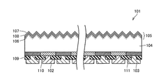
- FIG. 10 shows a schematic cross-sectional view of a conventional back electrode type solar cell disclosed in Patent Document 1 (Japanese Patent Publication No. 2008-532311).
- an n-type front side diffusion region 106 is formed on the light receiving surface of the conventional back electrode type solar cell 101 shown in FIG. 10 to form an FSF (Front Surface Field) structure.
- the light-receiving surface of the back electrode type solar cell 101 has a concavo-convex shape 105.
- a dielectric passivation layer 108 containing silicon dioxide and an antireflection coating 107 containing silicon nitride are n. They are formed in this order from the mold silicon wafer 104 side.
- n + regions 110 doped with n-type impurities and p + regions 111 doped with p-type impurities are alternately formed on the back surface of the n-type silicon wafer 104.
- An oxide layer 109 is formed on the back surface of 104.
- An n-type metal contact 102 is formed on the n + region 110 on the back surface of the n-type silicon wafer 104, and a p-type metal contact 103 is formed on the p + region 111.
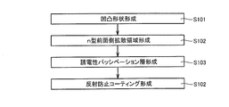
- FIG. 11 shows a flowchart of an assumed manufacturing method on the light-receiving surface side of the conventional back electrode type solar cell 101 shown in FIG.
- step S ⁇ b> 101 an uneven shape 105 is formed on the light receiving surface of the n-type silicon wafer 104.
- step S ⁇ b> 102 n-type front side diffusion regions 106 are formed by diffusing n-type impurities on the light-receiving surface of the n-type silicon wafer 104.
- step S ⁇ b> 103 a dielectric passivation layer 108 is formed on the n-type front side diffusion region 106.
- step S ⁇ b> 104 an antireflection coating 107 is formed on the dielectric passivation layer 108.
- the back electrode type solar cell 101 is formed by the method shown in the flowchart of FIG. 11, the number of steps increases, and thus the back electrode type solar cell 101 is efficiently manufactured. In addition, there is a problem that the characteristics of the back electrode type solar cell 101 are deteriorated because the amount of recombination current due to passivation on the light receiving surface side is increased.
- an object of the present invention is to provide a back electrode that can be efficiently manufactured with a reduced number of steps and that can reduce the amount of recombination current due to passivation on the light receiving surface side. It is in providing the manufacturing method of a solar cell, and a back electrode type solar cell.
- the present invention includes a step of applying a solution containing a compound containing a first conductivity type impurity, a titanium alkoxide, and an alcohol to one surface of a first conductivity type silicon substrate, and performing a first heat treatment on the solution in a nitrogen atmosphere. Performing a step of forming a light-receiving surface diffusion layer on the surface of the silicon substrate and forming an antireflection film on the surface of the silicon substrate; and performing a second heat treatment on the surface of the silicon substrate. Forming a light-receiving surface passivation film thereon, and a method for manufacturing a back electrode type solar cell.
- the heat treatment temperature of the surface of the silicon substrate is higher than 850 ° C. in the step of forming the light-receiving surface passivation film.
- the light-receiving surface passivation film is preferably a silicon oxide film.
- the manufacturing method of the back electrode type solar cell of the present invention further includes a step of forming a back surface passivation film on the second surface opposite to the surface of the silicon substrate.
- the sheet resistance of the light-receiving surface diffusion layer is preferably 100 ⁇ / ⁇ or more and less than 250 ⁇ / ⁇ .
- the present invention provides a first conductivity type silicon substrate, a first conductivity type electrode and a second conductivity type electrode provided on the back surface opposite to the light receiving surface of the silicon substrate, and a silicon substrate.
- a light receiving surface diffusion layer provided on the light receiving surface, a light receiving surface passivation film provided on the light receiving surface diffusion layer, and an antireflection film provided on the light receiving surface passivation film.
- the concentration of the first conductivity type impurity is higher than the concentration of the first conductivity type impurity in the silicon substrate, the sheet resistance of the light-receiving surface diffusion layer is not less than 100 ⁇ / ⁇ and less than 250 ⁇ / ⁇ , It is a back electrode type solar cell made of titanium oxide containing conductive impurities.
- the first conductivity type impurity contained in the antireflection film is an n-type impurity, and the n-type impurity is 15 mass% or more and 35 mass% of the antireflection film as phosphorus oxide. The following are preferably included.
- a method for manufacturing a back electrode type solar cell that can be efficiently manufactured with a reduced number of steps and that can reduce the amount of recombination current due to passivation on the light receiving surface side, and A back electrode type solar cell can be provided.
- FIG. 1 It is a typical top view of the back surface of the back surface electrode type solar cell of embodiment.
- A is a schematic cross-sectional view along II-II in FIG. 1
- (b) is a schematic enlarged cross-sectional view of a part of the light-receiving surface of the n-type silicon substrate shown in (a)
- (C) is a typical expanded sectional view illustrating the difference in thickness between the n ++ layer and the p + layer shown in (a).
- FIG. 1 is typical sectional drawing illustrated about an example of the manufacturing method of the back electrode type solar cell of embodiment. It is a cross-sectional structure of the sample produced in the Example. It is a flowchart of the manufacturing method of the sample shown in FIG. It is a figure which shows the relationship between the recombination electric current amount in an Example, and the formation temperature T of a silicon oxide film. It is a figure which shows the relationship between the sheet resistance and the formation temperature T of a silicon oxide film in an Example.
- (A) is an X-ray diffraction pattern of the titanium oxide film of the sample of the example, and (b) is an X-ray diffraction pattern of the titanium oxide film of the sample of the comparative example. It is typical sectional drawing of the conventional back surface electrode type solar cell currently disclosed by patent document 1.
- FIG. It is a flowchart of the manufacturing method assumed by the light-receiving surface side of the back electrode type solar cell shown in FIG.
- FIG. 1 shows a schematic plan view of the back surface of a back electrode type solar cell according to an embodiment which is an example of the back electrode type solar cell of the present invention.
- the back electrode type solar cell 1 shown in FIG. 1 includes a strip-shaped n-type electrode 2 and a strip-shaped p-type electrode 3 on the back surface opposite to the light-receiving surface of the n-type silicon substrate 4.
- the n-type electrode 2 and the p-type electrode 3 are alternately arranged on the back surface of the n-type silicon substrate 4.
- FIG. 2A shows a schematic cross-sectional view along II-II in FIG. 1, and FIG. 2B schematically shows a part of the light-receiving surface of the n-type silicon substrate 4 shown in FIG. 2A.
- FIG. 2 (c) is a schematic enlarged cross-sectional view illustrating the difference in thickness between the n ++ region 9 and the p + region 10 shown in FIG. 2 (a).
- an uneven shape 5 is formed on the light receiving surface of the n-type silicon substrate 4.
- the unevenness of the uneven shape 5 is, for example, on the order of several ⁇ m to several tens of ⁇ m.
- an n + region which is a light-receiving surface diffusion layer 6 formed by diffusing n-type impurities is formed as an FSF layer on the entire light-receiving surface of the n-type silicon substrate 4.
- the light-receiving surface diffusion layer 6 is a layer having the same n-type conductivity type as the n-type silicon substrate 4, and the n-type impurity concentration of the light-receiving surface diffusion layer 6 is higher than the n-type impurity concentration of the n-type silicon substrate 4. It is high.
- a light-receiving surface passivation film 13 is formed on the light-receiving surface diffusion layer 6.
- the light-receiving surface passivation film 13 is made of a silicon oxide film.
- the thickness of the light-receiving surface passivation film 13 can be set to, for example, 5 nm to 200 nm, preferably 5 nm to 60 nm.
- an antireflection film 12 is formed on the light receiving surface passivation film 13.
- the antireflection film 12 includes an n-type impurity having the same n-type conductivity as that of the n-type silicon substrate 4, for example, a titanium oxide film including phosphorus as the n-type impurity.
- the thickness of the antireflection film 12 can be, for example, not less than 10 nm and not more than 400 nm.
- Phosphorus in the antireflection film 12 is contained as a phosphorus oxide in an amount of 15% by mass to 35% by mass of the antireflection film 12.
- 15 mass% or more and 35 mass% or less of the anti-reflective film 12 is contained as a phosphorus oxide that the content of the phosphorus oxide in the anti-reflective film 12 is 15 mass% or more and 35 mass% of the whole anti-reflective film 12. It means the following.
- n ++ regions 9 as n-type semiconductor regions and p + regions 10 as p-type semiconductor regions are alternately adjacent to the back surface of the n-type silicon substrate 4. Is formed.
- a reverse bias reverse bias voltage
- the back electrode type solar cell 1 As with normal diodes, almost no current flows up to the breakdown voltage, and when a voltage higher than the breakdown voltage is applied, a large current (breakdown current) flows. 1 is not applied.
- a p + region 71 that is a p-type semiconductor region that is not in contact with the electrode is formed on the outermost side of the back surface of the n-type silicon substrate 4.
- the surface of the n ++ region 9 on the back surface of the n-type silicon substrate 4 is recessed from the surface of the region other than the n ++ region 9 on the back surface of the n-type silicon substrate 4. It arrange
- the surface of the n ++ region 9 is located shallower by the depth d than the surface of the p + region 10, and the depth d is, for example, on the order of several tens of nm. It is said. Further, an n-type electrode 2 is formed on the n ++ region 9, and a p-type electrode 3 is formed on the p + region 10.
- a second back surface passivation film 8 made of a silicon oxide film is formed on a part of the back surface of the n-type silicon substrate 4, and the first back surface passivation film 8 made of, for example, a silicon oxide film is formed on the second back surface passivation film 8.
- a back surface passivation film 11 is formed.
- a back surface passivation film 14 is formed from a laminate of the second back surface passivation film 8 and the first back surface passivation film 11.
- FIG. 3 shows a schematic plan view of the back surface of the n-type silicon substrate 4 when the n-type electrode 2, the p-type electrode 3 and the back surface passivation film 14 are removed from the back electrode type solar cell 1.
- no electrode is disposed on the outer peripheral edge of the back surface of the n-type silicon substrate 4, and a p + region 71, which is a p-type semiconductor region not in contact with the electrode, is formed (hereinafter referred to as n-type silicon).
- a semiconductor region formed on the outer peripheral edge of the back surface of the substrate 4 and not in contact with the electrode may be referred to as an “outer peripheral semiconductor region”.
- the p + region 71 which is an outer peripheral semiconductor region having a conductivity type different from that of the n + + region 9, is formed so as to surround the periphery of the n + + region 9 on the back surface of the n-type silicon substrate 4. Even if a semiconductor region of the first conductivity type or the second conductivity type is formed outside the formation region of the n ++ region 9 and the p + region 10, the semiconductor region, the n ++ region 9 and the p ++ region 9 It is electrically separated from the + region 10. Even if a reverse bias (reverse bias voltage) is applied to the back electrode type solar cell 1, the p + region 71 as the outer peripheral semiconductor region is not in contact with the electrode. It is possible to suppress the occurrence of leak current flowing into the electrode through the outer peripheral edge of 1.
- a reverse bias reverse bias voltage
- all n ++ regions 9 are connected to form one semiconductor region. However, not all n ++ regions 9 are necessarily connected. Further, in the example shown in FIG. 3, the p + region 10 is formed separately in a plurality, but may be connected.
- the back surface electrode type solar cell 1 of embodiment since the electrode of the both ends arrange
- a texture mask 21 is formed.
- the n-type silicon substrate 4 for example, a substrate made of n-type single crystal silicon having a thickness of 100 ⁇ m can be used.
- a silicon nitride film can be used as the texture mask 21.
- the texture mask 21 can be formed by, for example, a CVD (Chemical Vapor Deposition) method or a sputtering method.
- the uneven shape 5 is formed on the light receiving surface of the n-type silicon substrate 4.
- the uneven shape 5 can have a texture structure, for example.
- the uneven shape 5 is formed by etching the light-receiving surface of the n-type silicon substrate 4 with a solution in which isopropyl alcohol is added to an alkaline aqueous solution such as a sodium hydroxide aqueous solution or a potassium hydroxide aqueous solution and heated to 70 ° C. or higher and 80 ° C. or lower. Can be formed.
- an n ++ region 9 is formed on a part of the back surface of the n-type silicon substrate 4.
- the n ++ region 9 can be formed as follows, for example.
- n ++ region 9 is formed by diffusing phosphorus from diffusion mask 23 to the portion where the back surface of n-type silicon substrate 4 is exposed by vapor phase diffusion using POCl 3 .
- the thing containing a solvent, a thickener, and a silicon oxide precursor etc. can be used, for example.
- a method for applying the masking paste for example, an ink jet printing method or a screen printing method can be used.
- a silicon oxide film 24 is formed on the back surface and the light receiving surface of the n-type silicon substrate 4.
- the silicon oxide film 24 is formed by, for example, hydrofluoric acid using a glass layer formed by phosphorus diffusing into the diffusion mask 22, the diffusion mask 23, and the diffusion masks 22 and 23 formed on the n-type silicon substrate 4. After removal by treatment, it can be formed by thermal oxidation with oxygen or water vapor. Note that thermal oxidation of the n-type silicon substrate 4 with oxygen or water vapor can be performed by heat treatment in a state where the n-type silicon substrate 4 is placed in an oxygen atmosphere or water vapor atmosphere.
- the silicon oxide film 24 on the region where the n ++ region 9 on the back surface of the n-type silicon substrate 4 is formed (the silicon oxide film 24 on the n ++ region 9). ) Can be made thicker than the thickness of the silicon oxide film 24 on the region where the n ++ region 9 is not formed (the silicon oxide film 24 on the region other than the n ++ region 9).
- the silicon oxide film 24 having such a shape can be formed, when the silicon oxide film 24 is formed by performing thermal oxidation with water vapor at 900 ° C., the silicon oxide on the n ++ region 9 is formed.
- the film thickness of the film 24 can be set to 250 nm to 350 nm, and the film thickness of the silicon oxide film 24 on the region other than the n ++ region 9 can be set to 70 nm to 90 nm.
- the phosphorus concentration on the surface of the n ++ region 9 before thermal oxidation is 5 ⁇ 10 19 atoms / cm 3 or more
- the thermal oxidation treatment temperature range is 800 ° C. to 1000 ° C. by thermal oxidation with oxygen.
- the temperature is 800 ° C. to 950 ° C. by thermal oxidation with steam.
- the film thickness of the diffusion mask in the n ++ region 9 when forming the p + region 10 in the following process is preferably 60 nm or more.
- the difference in thickness between the thickness and the thickness of the silicon oxide film 24 on the region other than the n ++ region 9 is preferably 60 nm or more.
- the growth rate of the silicon oxide film 24 by thermal oxidation can be made different depending on the type and concentration of impurities diffused on the back surface of the n-type silicon substrate 4.
- the n-type impurity concentration on the back surface of the n-type silicon substrate 4 is high, the growth rate of the silicon oxide film 24 can be increased. Therefore, the thickness of the silicon oxide film 24 on the n ++ region 9 having an n-type impurity concentration higher than that of the n-type silicon substrate 4 is set to be other than the n ++ region 9 having an n-type impurity concentration lower than that of the n ++ region 9. It can be made thicker than the film thickness of the silicon oxide film 24 on this region.
- the silicon oxide film 24 is formed by bonding silicon and oxygen during thermal oxidation.
- a p + region 10 and a p + region 71 are formed on a part of the back surface of the n-type silicon substrate 4.
- p ⁇ +> region 10 and p ⁇ +> region 71 can be formed as follows, for example.
- the silicon oxide film 24 on the light receiving surface of the n-type silicon substrate 4 and the silicon oxide film 24 on the back surface other than the n ++ region 9 are removed by etching.
- the thickness of the silicon oxide film 24 on the n ++ region 9 on the back surface of the n-type silicon substrate 4 is thicker than the thickness of the silicon oxide film 24 on the region other than the n ++ region 9. Therefore, the silicon oxide film 24 can be left only on the n ++ region 9 on the back surface of the n-type silicon substrate 4.
- the thickness of the silicon oxide film 24 on the n ++ region 9 is changed. It can be about 120 nm.
- the silicon oxide film 24 is formed by thermal oxidation for 30 minutes with water vapor at 900 ° C. and hydrofluoric acid treatment is performed to remove the silicon oxide film 24 on the region other than the n ++ region 9, n
- the film thickness of the silicon oxide film 24 on the ++ region 9 can be about 120 nm.
- the silicon oxide film 24 is used as a diffusion mask when the p + region 10 and the p + region 71 are formed. It can function suitably as.
- a diffusion mask 25 such as a silicon oxide film is formed on the light-receiving surface of the n-type silicon substrate 4, and then a polymer obtained by reacting a boron compound with an organic polymer is formed on the back surface of the n-type silicon substrate 4 with an alcohol solvent After the solution dissolved in is applied and dried, boron, which is a p-type impurity, diffuses into the exposed portion of the back surface of the n-type silicon substrate 4 by heat treatment to form the p + region 10 and the p + region 71.
- boron which is a p-type impurity
- a first back surface passivation film 11 is formed on the back surface of the n-type silicon substrate 4.
- the first back surface passivation film 11 can be formed as follows, for example.
- the silicon oxide film 24 and the diffusion mask 25 formed on the n-type silicon substrate 4 and the glass layer formed by diffusing boron in the silicon oxide film 24 and the diffusion mask 25 are removed by hydrofluoric acid treatment.
- a first back surface passivation film 11 that also serves as a diffusion mask such as a silicon oxide film is formed on the back surface of the n-type silicon substrate 4 by, for example, a CVD method or a method such as SOG (spin on glass) coating and baking.
- a liquid mixture 27 containing at least a phosphorus compound, titanium alkoxide, and alcohol is applied to the light receiving surface of the n-type silicon substrate 4 by spin coating or the like and dried.
- the liquid mixture 27 is applied to form an n + region which is the light receiving surface diffusion layer 6 on the light receiving surface of the n-type silicon substrate 4 and to form a titanium oxide film containing phosphorus which becomes the antireflection film 12. Is done.
- phosphorus pentoxide can be used as the phosphorus compound of the mixed liquid
- tetraisopropyl titanate can be used as the titanium alkoxide
- isopropyl alcohol can be used as the alcohol, for example.
- a light-receiving surface diffusion layer 6 that is an n + region is formed on the light-receiving surface of the n-type silicon substrate 4, and light reception by the n-type silicon substrate 4 is performed.
- An antireflection film 12 is formed on the surface.
- the formation of the light-receiving surface diffusion layer 6 and the antireflection film 12 is performed by heat-treating (first heat treatment) the mixed liquid 27 applied to the light-receiving surface of the n-type silicon substrate 4 and dried in a nitrogen atmosphere.
- heat-treating first heat treatment
- phosphorus which is an n-type impurity, diffuses into the light-receiving surface of the n-type silicon substrate 4, thereby forming a light-receiving surface diffusion layer 6 over the entire light-receiving surface of the n-type silicon substrate 4, and the n-type silicon substrate.
- a titanium oxide film containing phosphorus to be the antireflection film 12 is formed on the light receiving surface 4.
- the sheet resistance of the light-receiving surface diffusion layer 6 is preferably 100 ⁇ / ⁇ or more and less than 250 ⁇ / ⁇ . In this case, the amount of recombination current due to the passivation property on the light-receiving surface side of the back electrode type solar cell 1 can be reduced, and the characteristics of the back electrode type solar cell 1 can be improved.
- a second back surface passivation film 8 is formed on the back surface of the n-type silicon substrate 4, and the light-receiving surface diffusion of the light-receiving surface of the n-type silicon substrate 4 is performed.
- a light-receiving surface passivation film 13 is formed on the layer 6.
- the second back surface passivation film 8 and the light-receiving surface passivation film 13 thermally oxidize the n-type silicon substrate 4 by heat treatment (second heat treatment) of the n-type silicon substrate 4 in an oxygen atmosphere or a water vapor atmosphere, for example. Can be formed.
- the second back surface passivation film 8 made of a silicon oxide film can be formed between the back surface of the n-type silicon substrate 4 and the first back surface passivation film 11, and the light receiving surface of the n-type silicon substrate 4 can receive light.
- a light-receiving surface passivation film 13 made of a silicon oxide film can be formed between the surface diffusion layer 6 and the antireflection film 12.
- the reason why the light-receiving surface passivation film 13 is formed between the light-receiving surface diffusion layer 6 and the antireflection film 12 is that the film thickness of the antireflection film 12 in the concave portion of the concavo-convex shape 5 on the light receiving surface increases and the antireflection film 12 is cracked, and it is considered that oxygen or water vapor enters from the portion where the crack is generated to grow a silicon oxide film as the light-receiving surface passivation film 13.
- the reason why the second back surface passivation film 8 is formed between the back surface of the n-type silicon substrate 4 and the first back surface passivation film 11 is that the first back surface passivation film 11 on the back surface of the n-type silicon substrate 4 is CVD. Since it is a film formed by the method or the like, it is considered that oxygen or water vapor passes through the inside of the first back surface passivation film 11 and thereby the silicon oxide film as the second back surface passivation film 8 grows.
- the gas is switched to form the light receiving surface passivation film 13 and the second back surface passivation film 8. It is preferable to perform the second heat treatment in an oxygen atmosphere or a water vapor atmosphere. In this case, since there is no need to perform an extra step between the first heat treatment and the second heat treatment, the number of steps can be reduced, and the back electrode type solar cell 1 can be efficiently manufactured. It tends to be possible.
- the heat treatment temperature of the surface of the n-type silicon substrate 4 at the time of forming the light-receiving surface passivation film 13 is preferably higher than 850 ° C. In this case, the amount of recombination current due to the passivation property on the light-receiving surface side of the back electrode type solar cell 1 can be reduced, and the characteristics of the back electrode type solar cell 1 can be improved.
- a part of the back surface passivation film 14 is removed to expose a part of the n ++ region 9 and a part of the p + region 10 from the back surface passivation film 14, respectively.
- the removal of a part of the back surface passivation film 14 can be performed, for example, by applying the etching paste to a part of the back surface passivation film 14 by a screen printing method or the like and then heating the etching paste. Thereafter, the etching paste can be removed, for example, by performing an acid treatment after ultrasonic cleaning.
- the etching paste includes, for example, at least one selected from the group consisting of phosphoric acid, hydrogen fluoride, ammonium fluoride, and ammonium hydrogen fluoride as an etching component, and also includes water, an organic solvent, and a thickener. Things can be used.
- the n-type electrode 2 is formed on the n ++ region 9 and the p-type electrode 3 is formed on the p + region 10.
- the n-type electrode 2 and the p-type electrode 3 are formed, for example, by applying a silver paste to a predetermined position of the back surface passivation film 14 by screen printing and then drying, and then baking the silver paste. be able to.
- the back electrode type solar cell 1 of embodiment can be manufactured.
- phosphorous which is an n-type impurity having the same conductivity type as that of the n-type silicon substrate 4 is formed on one surface of the n-type silicon substrate 4 used in the back electrode type solar cell 1.
- the antireflective film 12 and the light-receiving surface diffusion layer 6 that is an FSF layer are formed by applying a solution 27 containing a phosphorus compound containing, a titanium alkoxide, and alcohol and performing heat treatment. Therefore, in the present embodiment, it is not necessary to separately form the light-receiving surface diffusion layer 6 and the antireflection film 12, and therefore the back electrode type solar cell 1 can be efficiently manufactured by reducing the number of steps. Can do.
- the heat treatment for forming the light-receiving surface diffusion layer 6 and the antireflection film 12 is performed in a nitrogen atmosphere, it is caused by the passivation property on the light-receiving surface side of the back electrode type solar cell 1.
- the amount of recombination current can be reduced, and the characteristics of the back electrode solar cell 1 can be improved.
- the sheet resistance of the light receiving surface diffusion layer 6 provided on the light receiving surface of the n-type silicon substrate 4 is 100 ⁇ / ⁇ or more and less than 250 ⁇ / ⁇ .
- the antireflection film 12 is made of titanium oxide containing phosphorus. Therefore, since the amount of recombination current resulting from the passivation property on the light receiving surface side of the back electrode type solar cell 1 can be reduced, the characteristics of the back electrode type solar cell 1 can be improved.
- the light receiving surface side of the back electrode type solar cell 1 is provided.
- the amount of recombination current due to passivation can be further reduced, and the characteristics of the back electrode solar cell 1 can be further improved.
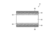
- FIG. 5 shows a cross-sectional structure of a sample 81 manufactured in this example.
- the sample 81 corresponds to an n-type silicon substrate 82, an n + region 83 corresponding to a light-receiving surface diffusion layer on both surfaces of the n-type silicon substrate 82, and a light-receiving surface passivation film and a back surface passivation film on the n + region 83.
- a silicon oxide film 84 and a titanium oxide film 85 containing phosphorus corresponding to an antireflection film are provided on the silicon oxide film 84.
- FIG. 6 shows a flowchart of a manufacturing method of the sample 81 shown in FIG.
- step S1 concavo-convex shapes (not shown in FIG. 5) were formed on both surfaces of the n-type silicon substrate 82, respectively.
- step S2 a mixed solution containing a phosphorus compound, titanium alkoxide and alcohol was applied onto the concavo-convex shapes on both sides of the n-type silicon substrate 82 and dried.
- diphosphorus pentoxide was used as the phosphorus compound
- tetraisopropyl titanate was used as the titanium alkoxide
- isopropyl alcohol was used as the alcohol.
- step S3 the mixed liquid on the concavo-convex shape on both surfaces of the n-type silicon substrate 82 is heat-treated to diffuse phosphorus on the surface of the n-type silicon substrate 82 to form an n + region 83.
- a titanium oxide film 85 containing phosphorus was formed on the surface of the n-type silicon substrate 82.
- step S 4 a silicon oxide film 84 was formed between the n + region 83 and the titanium oxide film 85 by thermally oxidizing both surfaces of the n-type silicon substrate 82 using oxygen. Thus, a sample 81 shown in FIG. 5 was produced.
- ⁇ Measurement of recombination current> The amount of recombination current of Sample 81 produced as described above was measured.
- the recombination current amount of the sample 81 was measured by a QSSPC (Quasi Steady State Photo Conductance) method using WTC-120 manufactured by Synton Consulting as a measuring instrument.
- FIG. 7 shows the measurement result of the recombination current amount of sample 81 when the formation temperature T of the silicon oxide film 84 in step S4 is changed to 850 ° C., 900 ° C., 950 ° C., and 1000 ° C., respectively.
- 7 represents the recombination current amount
- the horizontal axis in FIG. 7 represents the formation temperature T of the silicon oxide film 84.
- the recombination current amount of the sample 81 of the example manufactured by performing the heat treatment in step S3 in a nitrogen atmosphere is indicated by a circle, and the comparison is performed by performing the heat treatment in step S3 in an atmosphere containing oxygen.
- the recombination current amount of the sample 81 of the example is represented by a square mark.
- the recombination current amount in FIG. 7 is the recombination current of the sample 81 of the comparative example manufactured by performing the heat treatment in step S3 in an atmosphere containing oxygen and setting the formation temperature T of the silicon oxide film 84 in step S4 to 850 ° C. It is expressed as a relative value when the amount is 1.
- the amount of recombination current can be reduced as the formation temperature T of the silicon oxide film 84 in step S4 increases. Further, as shown in FIG. 7, in the sample 81 of the comparative example manufactured by performing the heat treatment in step S3 in an atmosphere containing oxygen, the recombination is performed even if the formation temperature T of the silicon oxide film 84 in step S4 is changed. The amount of current could not be reduced.
- the difference in the amount of recombination current between the sample 81 of the example and the sample 81 of the comparative example increases as the formation temperature T of the silicon oxide film 84 in step S4 increases.
- the recombination current amount of the sample 81 of the example is reduced at a temperature where the formation temperature T of the silicon oxide film 84 in step S4 is higher than 850 ° C., and the recombination current amount is reduced.
- the formation temperature T of the silicon oxide film 84 is preferably 900 ° C. or higher, and more preferably 950 ° C. or higher.
- FIG. 8 shows the measurement results of the sheet resistance of Sample 81 when the formation temperature T of the silicon oxide film 84 in Step S4 is changed to 850 ° C., 900 ° C., 950 ° C., and 1000 ° C., respectively.
- 8 represents the sheet resistance
- the horizontal axis in FIG. 8 represents the formation temperature T of the silicon oxide film 84.
- the sheet resistance of the sample 81 of the example produced by performing the heat treatment in step S3 in a nitrogen atmosphere is indicated by a circle, and the comparative example produced by performing the heat treatment in step S3 in an atmosphere containing oxygen.
- the sheet resistance of the sample 81 is represented by a square mark.
- the formation temperature of the silicon oxide film 84 in step S4 higher than 850 ° C. and lower than 1000 ° C. was confirmed to be able to suitably reduce the recombination current amount of the sample 81 of the example.
- the sheet resistance of the n + region 83 corresponding to the range of T was 100 ⁇ / ⁇ or more and less than 250 ⁇ / ⁇ .
- ⁇ Crystal structure analysis of titanium oxide film> The titanium oxide film 85 of the sample 81 of the example manufactured by performing the heat treatment of step S3 in a nitrogen atmosphere, and the titanium oxide film 85 of the sample 81 of the comparative example manufactured by performing the heat treatment of step S3 in an atmosphere containing oxygen.
- the crystal structure was analyzed by X-ray diffraction.
- the samples 81 of the example and the comparative example were prepared by setting the heat treatment temperature in step S3 to 920 ° C. and the formation temperature T of the silicon oxide film 84 in step S4 to 950 ° C., respectively.
- FIG. 9A shows an X-ray diffraction pattern of the titanium oxide film 85 of the sample 81 of the example.
- FIG. 9B shows an X-ray diffraction pattern of the titanium oxide film 85 of the sample 81 of the comparative example.
- the titanium oxide film 85 of the sample 81 of the example has an anatase type crystal structure
- the titanium oxide film of the sample 81 of the comparative example had a rutile crystal structure.
- the formation temperature of the silicon oxide film which is a light-receiving surface passivation film is higher than 850 ° C., preferably 900 ° C. or higher, more preferably 950 ° C. or higher, so that the light-receiving surface side of the back-electrode solar cell is passivated. It is possible to further reduce the amount of recombination current resulting from the above, and further improve the characteristics of the back electrode solar cell.
- the sheet resistance of the n + region which is the light-receiving surface diffusion layer after the formation of the silicon oxide film, which is the light-receiving surface passivation film
- the light-receiving surface of the back electrode type solar cell The amount of recombination current resulting from the side passivation can be further reduced, and the characteristics of the back electrode solar cell can be further improved.
- the case where an n-type silicon substrate is used has been described.
- a p-type silicon substrate can also be used.
- the light-receiving surface diffusion layer is a p + region having a p-type impurity concentration higher than that of the p-type silicon substrate
- the antireflection film is a film containing p-type impurities. It becomes.
- Other structures are the same as those described above for the n-type silicon substrate.
- an n + region in which an n-type electrode is formed and a p-type electrode are formed on the back surface of the back electrode type solar cell.
- the p ++ regions it is preferable that the total area of the n + regions, which are semiconductor regions having a conductivity type different from that of the p-type silicon substrate, be larger than the total area of the p ++ regions.
- the p ++ region on the back surface of the back electrode type solar cell may be separated in a direction perpendicular to the length direction, and at this time, between the separated p ++ regions, An n + region can be formed.
- the n + region may be separated in the direction perpendicular to the length direction, and at this time, a p ++ region can be formed between the separated n + regions.
- the concept of the back electrode type solar cell of the present invention includes only a back electrode type solar cell in which both the p-type electrode and the n-type electrode are formed only on one surface (back surface) of the semiconductor substrate.
- a solar cell having a configuration such as an MWT (Metal Wrap Through) type (a solar cell having a configuration in which a part of an electrode is disposed in a through hole provided in a semiconductor substrate) is also included.
- MWT Metal Wrap Through
- the manufacturing method of a back electrode type solar cell and the back electrode type solar cell according to the present invention can be widely applied to the manufacturing method of a back electrode type solar cell and the back electrode type solar cell in general.
- 1,14 back electrode type solar cell 2 n type electrode, 3 p type electrode, 4 n type silicon substrate, 5 uneven shape, 6 light receiving surface diffusion layer, 8 second back surface passivation film, 9 n ++ region, 10 p + region, 11 1st back surface passivation film, 12 antireflection film, 13 light receiving surface passivation film, 14 back surface passivation film, 21 texture mask, 22, 23, 25 diffusion mask, 24 silicon oxide film, 27 solution, 71 p + Region, 81 samples, 82 n-type silicon substrate, 83 n + region, 84 silicon oxide film, 85 titanium oxide film, 101 back electrode solar cell, 102 n-type metal contact, 103 p-type metal contact, 104 n Type silicon wafer, 105 uneven shape, 106 n-type front side diffusion region, 107 reflection Stop coating, 108 dielectric passivation layer, 109 oxide layer, 110 n + regions, 111 p + region.
Landscapes
- Photovoltaic Devices (AREA)
- Life Sciences & Earth Sciences (AREA)
- Sustainable Development (AREA)
Abstract
第1導電型のシリコン基板(4)の表面に第1導電型不純物を含む化合物とチタンアルコキシドとアルコールとを含む溶液(27)を塗布し、窒素雰囲気で溶液(27)を熱処理することにより受光面拡散層(6)および反射防止膜(12)を形成する裏面電極型太陽電池(1)の製造方法である。また、受光面拡散層(6)のシート抵抗が100Ω/□以上250Ω/□未満である裏面電極型太陽電池(1)である。
Description
本発明は、裏面電極型太陽電池の製造方法および裏面電極型太陽電池に関する。
太陽光エネルギを直接電気エネルギに変換する太陽電池は、近年、特に地球環境問題の観点から、次世代のエネルギ源としての期待が急激に高まっている。太陽電池としては、化合物半導体または有機材料を用いたものなど様々な種類があるが、現在主流となっているのは、シリコン結晶を用いたものである。
現在、最も多く製造および販売されている太陽電池は、太陽光が入射する側の面(受光面)と、受光面の反対側の面(裏面)とにそれぞれ電極が形成された構造のものである。
太陽電池の受光面に電極を形成した場合には、太陽光が電極によって吸収されることから、電極の形成面積の分だけ太陽電池の受光面に入射する太陽光の量が減少する。そのため、太陽電池の裏面のみに電極を形成した構造の裏面電極型太陽電池が開発されている。
図10に、特許文献1(特表2008-532311号公報)に開示されている従来の裏面電極型太陽電池の模式的な断面図を示す。
図10に示す従来の裏面電極型太陽電池101の受光面にはn型前面側拡散領域106が形成されて、FSF(Front Surface Field)構造が形成されている。また、裏面電極型太陽電池101の受光面は凹凸形状105となっており、凹凸形状105上には、二酸化ケイ素を含む誘電性パッシベーション層108と、窒化シリコンを含む反射防止コーティング107と、がn型シリコンウエハ104側から、この順序で形成されている。
また、n型シリコンウエハ104の裏面には、n型不純物がドープされたn+領域110と、p型不純物がドープされたp+領域111と、が交互に形成されており、n型シリコンウエハ104の裏面上には酸化物層109が形成されている。そして、n型シリコンウエハ104の裏面のn+領域110上にはn型用金属コンタクト102が形成されており、p+領域111上にはp型用金属コンタクト103が形成されている。
図11に、図10に示す従来の裏面電極型太陽電池101の受光面側の想定される製造方法のフローチャートを示す。
まず、ステップS101に示すように、n型シリコンウエハ104の受光面に凹凸形状105を形成する。次に、ステップS102に示すように、n型シリコンウエハ104の受光面にn型不純物を拡散することによって、n型前面側拡散領域106を形成する。次に、ステップS103に示すように、n型前面側拡散領域106上に誘電性パッシベーション層108を形成する。次に、ステップS104に示すように、誘電性パッシベーション層108上に反射防止コーティング107を形成する。
しかしながら、図11のフローチャートに示される方法によって、裏面電極型太陽電池101の受光面側の構造を形成した場合には、工程数が多くなるために裏面電極型太陽電池101を効率的に製造することができず、また受光面側のパッシベーション性に起因した再結合電流量が大きくなるために裏面電極型太陽電池101の特性が低下するという問題があった。
上記の事情に鑑みて、本発明の目的は、工程数を少なくして効率的に製造することができるとともに、受光面側のパッシベーション性に起因した再結合電流量を低減することができる裏面電極型太陽電池の製造方法および裏面電極型太陽電池を提供することにある。
本発明は、第1導電型のシリコン基板の一方の表面に、第1導電型不純物を含む化合物とチタンアルコキシドとアルコールとを含む溶液を塗布する工程と、窒素雰囲気で溶液に第1の熱処理を行なうことによって、シリコン基板の表面に受光面拡散層を形成するとともにシリコン基板の表面上に反射防止膜を形成する工程と、シリコン基板の表面に第2の熱処理を行なうことによって、シリコン基板の表面上に受光面パッシベーション膜を形成する工程と、を含む、裏面電極型太陽電池の製造方法である。
ここで、本発明の裏面電極型太陽電池の製造方法においては、受光面パッシベーション膜を形成する工程において、シリコン基板の表面の熱処理温度が850℃よりも高いことが好ましい。
また、本発明の裏面電極型太陽電池の製造方法において、受光面パッシベーション膜は酸化シリコン膜であることが好ましい。
また、本発明の裏面電極型太陽電池の製造方法は、シリコン基板の表面の反対側の第2の表面に裏面パッシベーション膜を形成する工程をさらに含むことが好ましい。
また、本発明の裏面電極型太陽電池の製造方法において、受光面拡散層のシート抵抗は100Ω/□以上250Ω/□未満であることが好ましい。
また、本発明の裏面電極型太陽電池の製造方法においては、第1の熱処理に引き続いて第2の熱処理を行なうことが好ましい。
さらに、本発明は、第1導電型のシリコン基板と、シリコン基板の受光面とは反対側の面である裏面に設けられた第1導電型用電極と第2導電型用電極と、シリコン基板の受光面に設けられた受光面拡散層と、受光面拡散層上に設けられた受光面パッシベーション膜と、受光面パッシベーション膜上に設けられた反射防止膜と、を備え、受光面拡散層における第1導電型不純物の濃度は、シリコン基板における第1導電型不純物の濃度よりも高く、受光面拡散層のシート抵抗が、100Ω/□以上250Ω/□未満であり、反射防止膜は、第1導電型不純物を含む酸化チタンからなる裏面電極型太陽電池である。
ここで、本発明の裏面電極型太陽電池において、反射防止膜に含まれる第1導電型不純物はn型不純物であり、n型不純物はリン酸化物として反射防止膜の15質量%以上35質量%以下含まれることが好ましい。
本発明によれば、工程数を少なくして効率的に製造することができるとともに、受光面側のパッシベーション性に起因した再結合電流量を低減することができる裏面電極型太陽電池の製造方法および裏面電極型太陽電池を提供することができる。
以下、本発明の実施の形態について説明する。なお、本発明の実施の形態の図面において、同一の参照符号は、同一部分または相当部分を表わすものとする。
図1に、本発明の裏面電極型太陽電池の一例である実施の形態の裏面電極型太陽電池の裏面の模式的な平面図を示す。図1に示す裏面電極型太陽電池1は、n型シリコン基板4の受光面とは反対側の裏面に、帯状のn型用電極2と、帯状のp型用電極3と、を備えており、n型用電極2とp型用電極3とはn型シリコン基板4の裏面において交互に配列されている。
図2(a)に図1のII-IIに沿った模式的な断面図を示し、図2(b)に図2(a)に示すn型シリコン基板4の受光面の一部の模式的な拡大断面図を示し、図2(c)に図2(a)に示すn++領域9とp+領域10との厚さの差を図解する模式的な拡大断面図を示す。図2(a)および図2(b)に示すように、n型シリコン基板4の受光面には凹凸形状5(テクスチャ構造)が形成されている。凹凸形状5の凹凸は、たとえば数μm~数十μmオーダーとされる。
図2(b)に示すように、n型シリコン基板4の受光面の全面にはn型不純物が拡散して形成された受光面拡散層6であるn+領域がFSF層として形成されている。受光面拡散層6は、n型シリコン基板4と同一のn型の導電型を有する層であって、受光面拡散層6のn型不純物濃度はn型シリコン基板4のn型不純物濃度よりも高くなっている。
また、図2(b)に示すように、受光面拡散層6上には受光面パッシベーション膜13が形成されている。ここで、受光面パッシベーション膜13は、酸化シリコン膜からなる。また、受光面パッシベーション膜13の厚さは、たとえば5nm以上200nm以下とすることができ、好ましくは5nm以上60nm以下とすることができる。
また、図2(b)に示すように、受光面パッシベーション膜13上には反射防止膜12が形成されている。ここで、反射防止膜12は、n型シリコン基板4と同一のn型の導電型となるn型不純物を含み、たとえばn型不純物としてリンを含む酸化チタン膜からなる。また、反射防止膜12の厚さは、たとえば10nm以上400nm以下とすることができる。
反射防止膜12中のリンは、リン酸化物として反射防止膜12の15質量%以上35質量%以下含まれている。なお、リン酸化物として反射防止膜12の15質量%以上35質量%以下含まれるとは、反射防止膜12中のリン酸化物の含有量が反射防止膜12全体の15質量%以上35質量%以下であることを意味する。
また、n型シリコン基板4の裏面には、図2(a)に示すように、n型半導体領域であるn++領域9とp型半導体領域であるp+領域10とが交互に隣接して形成されている。このように、n++領域9とp+領域10とが交互に隣接して形成されていることより、裏面電極型太陽電池1に逆方向のバイアス(逆バイアス電圧)が印加されたとき、通常のダイオードと同じように降伏電圧までは、ほとんど電流が流れず、降伏電圧よりも大きな電圧が印加されたときに、大きな電流(降伏電流)が流れ、それ以上の電圧は裏面電極型太陽電池1に印加されないという現象が起きる。この降伏電流は、n++領域9とp+領域10とが隣接している領域で流れるため、n++領域9とp+領域10とが交互に隣接されている裏面電極型太陽電池1においては裏面電極型太陽電池1の裏面全面に電流が流れることになる。そのため、裏面電極型太陽電池1には部分的に電圧が印加されず、局所的なリーク電流による発熱を避けることができる。
また、図2(a)に示すように、n型シリコン基板4の裏面の最も外側には、電極に接触していないp型半導体領域であるp+領域71が形成されている。また、n型シリコン基板4の裏面のn++領域9の表面は、n型シリコン基板4の裏面のn++領域9以外の領域の表面よりも窪んでおり、n++領域9とp+領域10とは凹状を形成するように配置されている。
ここで、図2(c)に示すように、n++領域9の表面は、p+領域10の表面よりも深さdだけ浅く位置しており、深さdは、たとえば数十nmオーダーとされる。さらに、n++領域9上にはn型用電極2が形成されており、p+領域10上にはp型用電極3が形成されている。
また、n型シリコン基板4の裏面の一部には、酸化シリコン膜からなる第2裏面パッシベーション膜8が形成されており、第2裏面パッシベーション膜8上にはたとえば酸化シリコン膜などからなる第1裏面パッシベーション膜11が形成されている。この第2裏面パッシベーション膜8と第1裏面パッシベーション膜11との積層体から裏面パッシベーション膜14が形成されている。
図3に、裏面電極型太陽電池1からn型用電極2、p型用電極3および裏面パッシベーション膜14を除去したときのn型シリコン基板4の裏面の模式的な平面図を示す。ここで、n型シリコン基板4の裏面の外周縁には電極が配置されておらず、電極に接触していないp型半導体領域であるp+領域71が形成されている(以下、n型シリコン基板4の裏面の外周縁に形成された、電極に接していない半導体領域を「外周縁半導体領域」ということもある。)。
このように、n型シリコン基板4の裏面のn++領域9の周囲を取り囲むようにして、n++領域9とは導電型の異なる外周縁半導体領域であるp+領域71を形成することによって、n++領域9とp+領域10との形成領域の外側に第1導電型または第2導電型の半導体領域が形成されたとしても、その半導体領域と、n++領域9およびp+領域10とは電気的に分離できている。そして、裏面電極型太陽電池1に逆方向のバイアス(逆バイアス電圧)が印加されたとしても、外周縁半導体領域としてのp+領域71は電極に接触していないことから、裏面電極型太陽電池1の外周縁を通って電極に流れ込むリーク電流の発生を抑えることができる。
なお、図3に示す例においては、n++領域9はすべて繋がって1つの半導体領域を形成しているが、必ずしも全部のn++領域9が繋がっていなくてもよい。さらに、図3に示す例においては、p+領域10は複数に分離して形成されているが、繋がっている箇所があってもよい。
また、実施の形態の裏面電極型太陽電池1においては、n型シリコン基板4の裏面において、最も外側に配置されている両端の電極がそれぞれn型用電極2であるため、裏面電極型太陽電池1の裏面を回転対称構造とすることが可能となる。そのため、裏面電極型太陽電池1を複数並べて太陽電池モジュールを作製する際に、図1に示す裏面電極型太陽電池1の裏面の上下が反対になってもいてもよい。
以下、図4(a)~図4(j)の模式的断面図を参照して、実施の形態の裏面電極型太陽電池1の製造方法の一例について説明する。
まず、図4(a)に示すように、n型シリコン基板4の受光面となる面(n型シリコン基板4の受光面)の反対側の面である裏面(n型シリコン基板4の裏面)にテクスチャマスク21を形成する。ここで、n型シリコン基板4としては、たとえば厚さ100μmのn型単結晶シリコンからなる基板を用いることができる。また、テクスチャマスク21としては、たとえば窒化シリコン膜などを用いることができる。また、テクスチャマスク21は、たとえばCVD(Chemical Vapor Deposition)法またはスパッタ法などによって形成することができる。
次に、図4(b)に示すように、n型シリコン基板4の受光面に凹凸形状5を形成する。凹凸形状5は、たとえば、テクスチャ構造とすることができる。凹凸形状5は、たとえば、水酸化ナトリウム水溶液または水酸化カリウム水溶液などのアルカリ水溶液にイソプロピルアルコールを添加して70℃以上80℃以下に加熱した溶液によりn型シリコン基板4の受光面をエッチングすることによって形成することができる。
次に、図4(c)に示すように、n型シリコン基板4の裏面の一部にn++領域9を形成する。ここで、n++領域9は、たとえば以下のようにして形成することができる。
まず、n型シリコン基板4の裏面のテクスチャマスク21を除去する。次に、n型シリコン基板4の受光面にたとえば酸化シリコン膜などの拡散マスク22を形成する。次に、n型シリコン基板4の裏面のn++領域9の形成領域以外の領域にマスキングペーストを塗布した後にマスキングペーストを熱処理することによって拡散マスク23を形成する。その後、POCl3を用いた気相拡散によって拡散マスク23からn型シリコン基板4の裏面が露出した箇所にリンを拡散させることによってn++領域9を形成する。
なお、マスキングペーストとしては、たとえば、溶剤、増粘剤および酸化シリコン前駆体を含むものなどを用いることができる。また、マスキングペーストの塗布方法としては、たとえば、インクジェット印刷法またはスクリーン印刷法などを用いることができる。
次に、図4(d)に示すように、n型シリコン基板4の裏面および受光面に酸化シリコン膜24を形成する。ここで、酸化シリコン膜24は、たとえば、n型シリコン基板4に形成された拡散マスク22、拡散マスク23および拡散マスク22,23にリンが拡散することによって形成されたガラス層をフッ化水素酸処理により除去した後、酸素または水蒸気で熱酸化することによって形成することができる。なお、n型シリコン基板4の酸素または水蒸気による熱酸化は、酸素雰囲気または水蒸気雰囲気中にn型シリコン基板4を設置した状態で熱処理することによって行なうことができる。
このとき、図4(d)に示すように、n型シリコン基板4の裏面のn++領域9が形成されている領域上の酸化シリコン膜24(n++領域9上の酸化シリコン膜24)の膜厚を、n++領域9が形成されていない領域上の酸化シリコン膜24(n++領域9以外の領域上の酸化シリコン膜24)の膜厚よりも厚くすることができる。このような形状の酸化シリコン膜24を形成することができる場合の一例としては、900℃で水蒸気による熱酸化を行なって酸化シリコン膜24を形成した場合に、n++領域9上の酸化シリコン膜24の膜厚を250nm~350nmとし、n++領域9以外の領域上の酸化シリコン膜24の膜厚を70nm~90nmとすることができる。ここで、熱酸化前のn++領域9の表面のリン濃度は5×10¹⁹個/cm3以上であり、熱酸化の処理温度の範囲としては、酸素による熱酸化で800℃~1000℃、水蒸気による熱酸化で800℃~950℃である。
なお、以下の工程におけるp+領域10形成時のn++領域9の拡散マスクの膜厚としては、60nm以上であることが好ましいことから、n++領域9上の酸化シリコン膜24の膜厚とn++領域9以外の領域上の酸化シリコン膜24の膜厚との膜厚差は60nm以上であることが好ましい。
また、熱酸化による酸化シリコン膜24の形成時に、n型シリコン基板4の裏面に拡散する不純物の種類と濃度とにより、熱酸化による酸化シリコン膜24の成長速度を異なるものとすることができ、特に、n型シリコン基板4の裏面におけるn型不純物濃度が高い場合には、酸化シリコン膜24の成長速度を速くすることができる。そのため、n型シリコン基板4よりもn型不純物濃度が高いn++領域9上の酸化シリコン膜24の膜厚を、n++領域9よりもn型不純物濃度が低いn++領域9以外の領域上の酸化シリコン膜24の膜厚よりも厚くすることができる。
なお、酸化シリコン膜24は、熱酸化時にシリコンと酸素とが結び付くことによって形成される。
次に、図4(e)に示すように、n型シリコン基板4の裏面の一部にp+領域10およびp+領域71を形成する。ここで、p+領域10およびp+領域71は、たとえば以下のようにして形成することができる。
まず、n型シリコン基板4の受光面の酸化シリコン膜24および裏面のn++領域9以外の領域上の酸化シリコン膜24をエッチングにより除去する。ここで、n型シリコン基板4の裏面のn++領域9上の酸化シリコン膜24の膜厚は、n++領域9以外の領域上の酸化シリコン膜24の膜厚よりも厚く形成されているため、n型シリコン基板4の裏面のn++領域9上のみに酸化シリコン膜24を残すことができる。n++領域9上の酸化シリコン膜24と、n++領域9以外の領域上の酸化シリコン膜24とのエッチングレートの差により、n++領域9上の酸化シリコン膜24の膜厚を120nm程度とすることができる。
例えば、900℃の水蒸気による30分の熱酸化で酸化シリコン膜24を形成し、n++領域9以外の領域上の酸化シリコン膜24を除去するためにフッ化水素酸処理をした場合、n++領域9上の酸化シリコン膜24の膜厚を120nm程度とすることができる。なお、上述したように、n++領域9上の酸化シリコン膜24の膜厚が60nm以上である場合には、酸化シリコン膜24はp+領域10およびp+領域71の形成時の拡散マスクとして好適に機能することができる。
さらに、n型シリコン基板4の受光面に酸化シリコン膜等の拡散マスク25を形成し、その後、n型シリコン基板4の裏面に、有機性高分子にホウ素化合物を反応させたポリマーをアルコール系溶媒に溶解させた溶液を塗布し、乾燥後、熱処理によりn型シリコン基板4の裏面の露出した箇所にp型不純物であるボロンが拡散して、p+領域10とp+領域71とが形成される。
次に、図4(f)に示すように、n型シリコン基板4の裏面に第1裏面パッシベーション膜11を形成する。ここで、第1裏面パッシベーション膜11は、たとえば以下のようにして形成することができる。
まず、n型シリコン基板4に形成された酸化シリコン膜24、拡散マスク25、ならびに酸化シリコン膜24および拡散マスク25にボロンが拡散して形成されたガラス層をフッ化水素酸処理により除去する。
次に、n型シリコン基板4の裏面に酸化シリコン膜等の拡散マスクを兼ねた第1裏面パッシベーション膜11を、たとえばCVD法またはSOG(スピンオングラス)の塗布および焼成などの方法により形成する。
次に、n型シリコン基板4の受光面にリン化合物、チタンアルコキシド、およびアルコールを少なくとも含む混合液27をスピン塗布等により塗布し、乾燥させる。ここで、混合液27は、n型シリコン基板4の受光面に受光面拡散層6であるn+領域を形成するとともに、反射防止膜12となるリンを含む酸化チタン膜を形成するために塗布される。また、混合液27のリン化合物としてはたとえば五酸化リンを用いることができ、チタンアルコキシドとしてはたとえばテトライソプロピルチタネートを用いることができ、およびアルコールとしてはたとえばイソプロピルアルコールを用いることができる。
次に、図4(g)および図4(j)に示すように、n型シリコン基板4の受光面にn+領域である受光面拡散層6を形成するとともに、n型シリコン基板4の受光面上におよび反射防止膜12を形成する。
受光面拡散層6および反射防止膜12の形成は、n型シリコン基板4の受光面に塗布されて乾燥された混合液27を窒素雰囲気で熱処理(第1の熱処理)することにより行なわれる。この熱処理により、n型不純物であるリンがn型シリコン基板4の受光面に拡散することによって、n型シリコン基板4の受光面全面に受光面拡散層6が形成されるとともに、n型シリコン基板4の受光面上に反射防止膜12となるリンを含有した酸化チタン膜が形成される。
ここで、受光面拡散層6のシート抵抗は、100Ω/□以上250Ω/□未満であることが好ましい。この場合には、裏面電極型太陽電池1の受光面側のパッシベーション性に起因した再結合電流量を低減して、裏面電極型太陽電池1の特性を向上することができる。
次に、図4(g)および図4(j)に示すように、n型シリコン基板4の裏面に第2裏面パッシベーション膜8を形成するとともに、n型シリコン基板4の受光面の受光面拡散層6上に受光面パッシベーション膜13を形成する。
ここで、第2裏面パッシベーション膜8および受光面パッシベーション膜13は、たとえば酸素雰囲気または水蒸気雰囲気で、n型シリコン基板4の熱処理(第2の熱処理)により、n型シリコン基板4を熱酸化することによって形成することができる。これによって、n型シリコン基板4の裏面と第1裏面パッシベーション膜11との間に酸化シリコン膜からなる第2裏面パッシベーション膜8を形成することができるとともに、n型シリコン基板4の受光面の受光面拡散層6と反射防止膜12との間に酸化シリコン膜からなる受光面パッシベーション膜13を形成することができる。
受光面拡散層6と反射防止膜12との間に受光面パッシベーション膜13が形成される理由としては、受光面の凹凸形状5の凹部における反射防止膜12の膜厚が厚くなって反射防止膜12にクラックが生じ、そのクラックが生じている箇所から酸素または水蒸気が入り込んで受光面パッシベーション膜13である酸化シリコン膜が成長すると考えられる。また、受光面の凹凸形状5の凸部では反射防止膜12の膜厚が薄いため、酸素または水蒸気が透過し、受光面パッシベーション膜13である酸化シリコン膜が成長すると考えられる。
さらに、n型シリコン基板4の裏面と第1裏面パッシベーション膜11との間に第2裏面パッシベーション膜8が形成される理由としては、n型シリコン基板4の裏面の第1裏面パッシベーション膜11はCVD法等で形成した膜であるため、第1裏面パッシベーション膜11の内部に酸素または水蒸気が透過し、これにより、第2裏面パッシベーション膜8である酸化シリコン膜が成長すると考えられる。
なお、受光面拡散層6および反射防止膜12を形成するための窒素雰囲気における第1の熱処理に引き続いて、ガスを切り替えて、受光面パッシベーション膜13および第2裏面パッシベーション膜8を形成するための酸素雰囲気または水蒸気雰囲気における第2の熱処理を行なうことが好ましい。この場合には、第1の熱処理と第2の熱処理との間に余分な工程を行なう必要がないため、工程数を減らすことができ、裏面電極型太陽電池1を効率的に製造することができる傾向にある。
また、受光面パッシベーション膜13の形成時におけるn型シリコン基板4の表面の熱処理温度は、850℃よりも高いことが好ましい。この場合には、裏面電極型太陽電池1の受光面側のパッシベーション性に起因した再結合電流量を低減して、裏面電極型太陽電池1の特性を向上することができる。
次に、図4(h)に示すように、裏面パッシベーション膜14の一部を除去して、裏面パッシベーション膜14からn++領域9の一部およびp+領域10の一部をそれぞれ露出させる。
ここで、裏面パッシベーション膜14の一部の除去は、たとえば、裏面パッシベーション膜14の一部にエッチングペーストをスクリーン印刷法等によって塗布した後にエッチングペーストを加熱することなどによって行なうことができる。その後、エッチングペーストは、たとえば、超音波洗浄した後に酸処理することによって除去することができる。エッチングペーストとしては、たとえば、エッチング成分として、リン酸、フッ化水素、フッ化アンモニウムおよびフッ化水素アンモニウムからなる群から選択された少なくとも1種を含むとともに、水、有機溶媒および増粘剤を含むものなどを用いることができる。
次に、図4(i)に示すように、n++領域9上にn型用電極2を形成するとともに、p+領域10上にp型用電極3を形成する。
ここで、n型用電極2およびp型用電極3は、たとえば、裏面パッシベーション膜14の所定の位置に銀ペーストをスクリーン印刷により塗布した後に乾燥させ、その後、銀ペーストを焼成することにより形成することができる。以上により、実施の形態の裏面電極型太陽電池1を製造することができる。
上記のように、本実施の形態においては、裏面電極型太陽電池1に用いられるn型シリコン基板4の一方の表面に、n型シリコン基板4と同一の導電型であるn型不純物であるリンを含むリン化合物と、チタンアルコキシドと、アルコールとを含む溶液27を塗布し、熱処理することによって、反射防止膜12とFSF層である受光面拡散層6とを形成している。そのため、本実施の形態においては、受光面拡散層6と反射防止膜12とを別々に形成する必要がないため、工程数を少なくして、裏面電極型太陽電池1を効率的に製造することができる。
また、本実施の形態においては、受光面拡散層6と反射防止膜12とを形成するための熱処理を窒素雰囲気で行なっているため、裏面電極型太陽電池1の受光面側のパッシベーション性に起因した再結合電流量を低減することができ、裏面電極型太陽電池1の特性を向上することができる。
また、上記のようにして製造された裏面電極型太陽電池1においては、n型シリコン基板4の受光面に設けられた受光面拡散層6のシート抵抗が100Ω/□以上250Ω/□未満であり、反射防止膜12がリンを含む酸化チタンから構成されている。そのため、裏面電極型太陽電池1の受光面側のパッシベーション性に起因した再結合電流量を低減することができることから、裏面電極型太陽電池1の特性を向上することができる。
特に、反射防止膜12中に、リンなどのn型不純物がリン酸化物として反射防止膜12の15質量%以上35質量%以下含まれる場合には、裏面電極型太陽電池1の受光面側のパッシベーション性に起因した再結合電流量をさらに低減することができ、裏面電極型太陽電池1の特性をさらに向上することができる。
<サンプルの作製>
図5に、本実施例で作製したサンプル81の断面構造を示す。サンプル81は、n型シリコン基板82と、n型シリコン基板82の両面にそれぞれ受光面拡散層に相当するn+領域83と、n+領域83上に受光面パッシベーション膜および裏面パッシベーション膜に相当する酸化シリコン膜84と、酸化シリコン膜84上に反射防止膜に相当するリンを含有する酸化チタン膜85と、を備えている。
図5に、本実施例で作製したサンプル81の断面構造を示す。サンプル81は、n型シリコン基板82と、n型シリコン基板82の両面にそれぞれ受光面拡散層に相当するn+領域83と、n+領域83上に受光面パッシベーション膜および裏面パッシベーション膜に相当する酸化シリコン膜84と、酸化シリコン膜84上に反射防止膜に相当するリンを含有する酸化チタン膜85と、を備えている。
ここで、図5に示すサンプル81は、以下のようにして作製した。図6に、図5に示すサンプル81の製造方法のフローチャートを示す。
まず、ステップS1に示すように、n型シリコン基板82の両面にそれぞれ凹凸形状(図5においては図示せず)を形成した。
次に、ステップS2に示すように、n型シリコン基板82の両面の凹凸形状上に、リン化合物、チタンアルコキシドおよびアルコールを含む混合液を塗布して乾燥させた。ここで、リン化合物としては五酸化二リンを用い、チタンアルコキシドとしてはテトライソプロピルチタネートを用い、アルコールとしてはイソプロピルアルコールを用いた。
次に、ステップS3に示すように、n型シリコン基板82の両面の凹凸形状上の混合液を熱処理することによって、n型シリコン基板82の表面にリンを拡散させてn+領域83を形成するとともに、n型シリコン基板82の表面上にリンを含有する酸化チタン膜85を形成した。
次に、ステップS4に示すように、n型シリコン基板82の両面を酸素を用いて熱酸化することによって、n+領域83と酸化チタン膜85との間に酸化シリコン膜84を形成した。これにより、図5に示すサンプル81を作製した。
<再結合電流量の測定>
上記のようにして作製したサンプル81の再結合電流量を測定した。サンプル81の再結合電流量は、測定器としてシントンコンサルティング社製のWTC-120を用いたQSSPC(Quasi Steady State Photo Conductance)法により測定した。
上記のようにして作製したサンプル81の再結合電流量を測定した。サンプル81の再結合電流量は、測定器としてシントンコンサルティング社製のWTC-120を用いたQSSPC(Quasi Steady State Photo Conductance)法により測定した。
図7に、ステップS4の酸化シリコン膜84の形成温度Tを850℃、900℃、950℃および1000℃にそれぞれ変えたときのサンプル81の再結合電流量の測定結果を示す。なお、図7の縦軸は再結合電流量を示し、図7の横軸は酸化シリコン膜84の形成温度Tを示している。また、図7においては、ステップS3の熱処理を窒素雰囲気で行なって作製した実施例のサンプル81の再結合電流量を丸印で表わし、ステップS3の熱処理を酸素を含む雰囲気で行なって作製した比較例のサンプル81の再結合電流量を四角印で表わしている。また、図7の再結合電流量は、ステップS3の熱処理を酸素を含む雰囲気で行ない、かつステップS4の酸化シリコン膜84の形成温度Tを850℃として作製した比較例のサンプル81の再結合電流量を1としたときの相対値で表わされている。
図7に示すように、ステップS3の熱処理を窒素雰囲気で行なって作製した実施例のサンプル81においては、ステップS4の酸化シリコン膜84の形成温度Tが高くなるほど再結合電流量を低減できた。また、図7に示すように、ステップS3の熱処理を酸素を含む雰囲気で行なって作製した比較例のサンプル81においては、ステップS4の酸化シリコン膜84の形成温度Tを変化させても、再結合電流量を低減することはできなかった。
また、図7に示すように、実施例のサンプル81と、比較例のサンプル81との再結合電流量の差異は、ステップS4の酸化シリコン膜84の形成温度Tが高くなるほど大きくなっていた。
さらに、図7に示すように、実施例のサンプル81の再結合電流量は、ステップS4の酸化シリコン膜84の形成温度Tが850℃よりも高い温度で低減しており、再結合電流量を低減する観点からは、酸化シリコン膜84の形成温度Tは900℃以上であることが好ましく、950℃以上であることがより好ましいことがわかった。
以上の結果により、ステップS3の熱処理の雰囲気およびステップS4の酸化シリコン膜84の形成温度Tが、サンプル81の再結合電流量に大きく影響することがわかった。
<シート抵抗の測定>
上記のようにして作製したサンプル81の再結合電流量の測定後に、サンプル81の両面の酸化シリコン膜84および酸化チタン膜85をそれぞれ除去し、さらに片面のn+領域83を除去して、除去していないn+領域83のシート抵抗(Ω/□)を測定した。
上記のようにして作製したサンプル81の再結合電流量の測定後に、サンプル81の両面の酸化シリコン膜84および酸化チタン膜85をそれぞれ除去し、さらに片面のn+領域83を除去して、除去していないn+領域83のシート抵抗(Ω/□)を測定した。
図8に、ステップS4の酸化シリコン膜84の形成温度Tを850℃、900℃、950℃および1000℃にそれぞれ変えたときのサンプル81のシート抵抗の測定結果を示す。なお、図8の縦軸はシート抵抗を示し、図8の横軸は酸化シリコン膜84の形成温度Tを示している。また、図8においては、ステップS3の熱処理を窒素雰囲気で行なって作製した実施例のサンプル81のシート抵抗を丸印で表わし、ステップS3の熱処理を酸素を含む雰囲気で行なって作製した比較例のサンプル81のシート抵抗を四角印で表わしている。
図8に示すように、ステップS3の熱処理を窒素雰囲気で行なって作製した実施例のサンプル81においては、ステップS3の熱処理を酸素を含む雰囲気で行なって作製した比較例のサンプル81と比べて、シート抵抗を低減できることがわかった。これは、酸素を含む雰囲気における熱処理では、n型不純物であるリンがn型シリコン基板82の表面に偏析して、偏析したリンによる欠陥により再結合電流量を低減できなかったものと考えられる。
また、上記の再結合電流量の測定において、実施例のサンプル81の再結合電流量を好適に低減できることが確認できた850℃よりも高く1000℃以下のステップS4の酸化シリコン膜84の形成温度Tの範囲に対応するn+領域83のシート抵抗は、100Ω/□以上250Ω/□未満であった。
<酸化チタン膜の結晶構造解析>
ステップS3の熱処理を窒素雰囲気で行なって作製した実施例のサンプル81の酸化チタン膜85と、ステップS3の熱処理を酸素を含む雰囲気で行なって作製した比較例のサンプル81の酸化チタン膜85との結晶構造をX線回折法により解析した。ここで、実施例および比較例のサンプル81は、それぞれ、ステップS3の熱処理温度を920℃とし、ステップS4の酸化シリコン膜84の形成温度Tを950℃として作製したものを用いた。
ステップS3の熱処理を窒素雰囲気で行なって作製した実施例のサンプル81の酸化チタン膜85と、ステップS3の熱処理を酸素を含む雰囲気で行なって作製した比較例のサンプル81の酸化チタン膜85との結晶構造をX線回折法により解析した。ここで、実施例および比較例のサンプル81は、それぞれ、ステップS3の熱処理温度を920℃とし、ステップS4の酸化シリコン膜84の形成温度Tを950℃として作製したものを用いた。
図9(a)に、実施例のサンプル81の酸化チタン膜85のX線回折パターンを示す。また、図9(b)に、比較例のサンプル81の酸化チタン膜85のX線回折パターンを示す。
図9(a)に示すように、実施例のサンプル81の酸化チタン膜85はアナタース型の結晶構造を有しており、図9(b)に示すように、比較例のサンプル81の酸化チタン膜85は、ルチル型の結晶構造を有していた。
<結果>
以上の結果から、受光面拡散層であるn+領域および反射防止膜であるリンを含有した酸化チタン膜の形成時の熱処理を窒素雰囲気で行なった場合には、工程数を低減して裏面電極型太陽電池を効率的に製造できるとともに、酸素を含む雰囲気で行なった場合と比べて裏面電極型太陽電池の受光面側のパッシベーション性に起因した再結合電流量を低減することができることから、裏面電極型太陽電池の特性を向上することができる。
以上の結果から、受光面拡散層であるn+領域および反射防止膜であるリンを含有した酸化チタン膜の形成時の熱処理を窒素雰囲気で行なった場合には、工程数を低減して裏面電極型太陽電池を効率的に製造できるとともに、酸素を含む雰囲気で行なった場合と比べて裏面電極型太陽電池の受光面側のパッシベーション性に起因した再結合電流量を低減することができることから、裏面電極型太陽電池の特性を向上することができる。
また、受光面パッシベーション膜である酸化シリコン膜の形成温度を850℃よりも高く、好ましくは900℃以上、より好ましくは950℃以上とすることによって、裏面電極型太陽電池の受光面側のパッシベーション性に起因した再結合電流量をさらに低減することができ、裏面電極型太陽電池の特性をさらに向上することができる。
また、受光面パッシベーション膜である酸化シリコン膜の形成後の受光面拡散層であるn+領域のシート抵抗が100Ω/□以上250Ω/□未満である場合にも、裏面電極型太陽電池の受光面側のパッシベーション性に起因した再結合電流量をさらに低減することができ、裏面電極型太陽電池の特性をさらに向上することができる。
なお、上記においては、n型シリコン基板を用いた場合について説明したが、p型シリコン基板を用いることもできる。n型シリコン基板に代えてp型シリコン基板を用いた場合には、受光面拡散層はp型シリコン基板よりもp型不純物濃度が高いp+領域となり、反射防止膜はp型不純物を含む膜となる。その他の構造は、n型シリコン基板について記載した上記構造と同様である。
また、p型シリコン基板を用いる場合には、より大きな短絡電流量を得るために、裏面電極型太陽電池の裏面において、n型用電極が形成されたn+領域およびp型用電極が形成されたp++領域のうち、p型シリコン基板とは異なる導電型の半導体領域であるn+領域の合計面積を、p++領域の合計面積よりも大きくすることが好ましい。また、この場合には、裏面電極型太陽電池の裏面のp++領域がその長さ方向に対して垂直方向に分離されていてもよく、このとき、分離されたp++領域間にはn+領域を形成することができる。また、この場合に、n+領域がその長さ方向に対して垂直方向に分離されていてもよく、このとき、分離されたn+領域間にはp++領域を形成することができる。
さらに、本発明の裏面電極型太陽電池の概念には、半導体基板の一方の表面(裏面)のみにp型用電極およびn型用電極の双方が形成された構成の裏面電極型太陽電池だけでなく、MWT(Metal Wrap Through)型(半導体基板に設けられた貫通孔に電極の一部を配置した構成の太陽電池)などの構成の太陽電池も含まれる。
以上のように本発明の実施の形態および実施例について説明を行なったが、上述の各実施の形態および各実施例の構成を適宜組み合わせることも当初から予定している。
今回開示された実施の形態および実施例はすべての点で例示であって制限的なものではないと考えられるべきである。本発明の範囲は上記した説明ではなくて請求の範囲によって示され、請求の範囲と均等の意味および範囲内でのすべての変更が含まれることが意図される。
本発明に係る裏面電極型太陽電池の製造方法および裏面電極型太陽電池は、裏面電極型太陽電池の製造方法および裏面電極型太陽電池の全般に広く適用することができる。
1,14 裏面電極型太陽電池、2 n型用電極、3 p型用電極、4 n型シリコン基板、5 凹凸形状、6 受光面拡散層、8 第2裏面パッシベーション膜、9 n++領域、10 p+領域、11 第1裏面パッシベーション膜、12 反射防止膜、13 受光面パッシベーション膜、14 裏面パッシベーション膜、21 テクスチャマスク、22,23,25 拡散マスク、24 酸化シリコン膜、27 溶液、71 p+領域、81 サンプル、82 n型シリコン基板、83 n+領域、84 酸化シリコン膜、85 酸化チタン膜、101 裏面電極型太陽電池、102 n型用金属コンタクト、103 p型用金属コンタクト、104 n型シリコンウエハ、105 凹凸形状、106 n型前面側拡散領域、107 反射防止コーティング、108 誘電性パッシベーション層、109 酸化物層、110 n+領域、111 p+領域。
Claims (8)
- 第1導電型のシリコン基板(4)の一方の表面に、第1導電型不純物を含む化合物とチタンアルコキシドとアルコールとを含む溶液(27)を塗布する工程と、
窒素雰囲気で前記溶液(27)に第1の熱処理を行なうことによって、前記シリコン基板(4)の前記表面に受光面拡散層(6)を形成するとともに前記シリコン基板(4)の前記表面上に反射防止膜(12)を形成する工程と、
前記シリコン基板(4)の前記表面に第2の熱処理を行なうことによって、前記シリコン基板(4)の前記表面上に受光面パッシベーション膜(13)を形成する工程と、を含む、裏面電極型太陽電池(1)の製造方法。 - 前記受光面パッシベーション膜(13)を形成する工程において、前記シリコン基板(4)の前記表面の熱処理温度は、850℃よりも高い、請求項1に記載の裏面電極型太陽電池(1)の製造方法。
- 前記受光面パッシベーション膜(13)は、酸化シリコン膜である、請求項1または2に記載の裏面電極型太陽電池(1)の製造方法。
- 前記シリコン基板(4)の前記表面の反対側の第2の表面に裏面パッシベーション膜(8)を形成する工程をさらに含む、請求項1から3のいずれかに記載の裏面電極型太陽電池(1)の製造方法。
- 前記受光面拡散層(6)のシート抵抗が、100Ω/□以上250Ω/□未満である、請求項1から4のいずれかに記載の裏面電極型太陽電池(1)の製造方法。
- 前記第1の熱処理に引き続いて前記第2の熱処理を行なう、請求項1から5のいずれかに記載の裏面電極型太陽電池(1)の製造方法。
- 第1導電型のシリコン基板(4)と、
前記シリコン基板(4)の受光面とは反対側の面である裏面に設けられた、第1導電型用電極(2)と、第2導電型用電極(3)と、
前記シリコン基板(4)の前記受光面に設けられた受光面拡散層(6)と、
前記受光面拡散層(6)上に設けられた受光面パッシベーション膜(13)と、
前記受光面パッシベーション膜(13)上に設けられた反射防止膜(12)と、を備え、
前記受光面拡散層(6)における第1導電型不純物の濃度は、前記シリコン基板(4)における第1導電型不純物の濃度よりも高く、
前記受光面拡散層(6)のシート抵抗が、100Ω/□以上250Ω/□未満であり、
前記反射防止膜(12)は、第1導電型不純物を含む酸化チタンからなる、裏面電極型太陽電池(1)。 - 前記反射防止膜(12)に含まれる前記第1導電型不純物はn型不純物であり、
前記n型不純物はリン酸化物として前記反射防止膜(12)の15質量%以上35質量%以下含まれる、請求項7に記載の裏面電極型太陽電池(1)。
Priority Applications (2)
| Application Number | Priority Date | Filing Date | Title |
|---|---|---|---|
| US13/990,538 US20130247980A1 (en) | 2010-12-06 | 2011-12-02 | Method for fabricating back electrode type solar cell, and back electrode type solar cell |
| CN2011800587316A CN103299432A (zh) | 2010-12-06 | 2011-12-02 | 背面电极型太阳能电池的制造方法及背面电极型太阳能电池 |
Applications Claiming Priority (2)
| Application Number | Priority Date | Filing Date | Title |
|---|---|---|---|
| JP2010271134A JP5723143B2 (ja) | 2010-12-06 | 2010-12-06 | 裏面電極型太陽電池の製造方法、および裏面電極型太陽電池 |
| JP2010-271134 | 2010-12-06 |
Publications (1)
| Publication Number | Publication Date |
|---|---|
| WO2012077597A1 true WO2012077597A1 (ja) | 2012-06-14 |
Family
ID=46207086
Family Applications (1)
| Application Number | Title | Priority Date | Filing Date |
|---|---|---|---|
| PCT/JP2011/077912 Ceased WO2012077597A1 (ja) | 2010-12-06 | 2011-12-02 | 裏面電極型太陽電池の製造方法および裏面電極型太陽電池 |
Country Status (4)
| Country | Link |
|---|---|
| US (1) | US20130247980A1 (ja) |
| JP (1) | JP5723143B2 (ja) |
| CN (1) | CN103299432A (ja) |
| WO (1) | WO2012077597A1 (ja) |
Cited By (1)
| Publication number | Priority date | Publication date | Assignee | Title |
|---|---|---|---|---|
| WO2014044924A1 (en) * | 2012-09-24 | 2014-03-27 | Optitune Oy | A method of modifying an n-type silicon substrate |
Families Citing this family (6)
| Publication number | Priority date | Publication date | Assignee | Title |
|---|---|---|---|---|
| US20150280018A1 (en) * | 2014-03-26 | 2015-10-01 | Seung Bum Rim | Passivation of light-receiving surfaces of solar cells |
| WO2015151288A1 (ja) * | 2014-04-04 | 2015-10-08 | 三菱電機株式会社 | 太陽電池の製造方法および太陽電池 |
| JP6502651B2 (ja) | 2014-11-13 | 2019-04-17 | 信越化学工業株式会社 | 太陽電池の製造方法及び太陽電池モジュールの製造方法 |
| WO2017099020A1 (ja) * | 2015-12-07 | 2017-06-15 | 東レ株式会社 | 半導体素子の製造方法および太陽電池の製造方法 |
| MY190851A (en) | 2016-06-13 | 2022-05-12 | Shinetsu Chemical Co | Solar cell and method for producing solar cell |
| CN108767024B (zh) * | 2018-08-15 | 2024-01-26 | 浙江晶科能源有限公司 | 一种光伏组件 |
Citations (13)
| Publication number | Priority date | Publication date | Assignee | Title |
|---|---|---|---|---|
| JPS5660075A (en) * | 1979-08-14 | 1981-05-23 | Westinghouse Electric Corp | Method of coating reflection preventive film on silicon |
| JPS58191478A (ja) * | 1982-05-04 | 1983-11-08 | Matsushita Electric Ind Co Ltd | 太陽電池の反射防止膜形成法 |
| JPS63283172A (ja) * | 1987-05-15 | 1988-11-21 | Sharp Corp | 太陽電池の製造方法 |
| JPH07221333A (ja) * | 1994-01-28 | 1995-08-18 | Sharp Corp | 太陽電池の製造方法 |
| JPH09191118A (ja) * | 1996-01-11 | 1997-07-22 | Shin Etsu Chem Co Ltd | 太陽電池の製造方法 |
| JPH1012907A (ja) * | 1996-06-20 | 1998-01-16 | Sharp Corp | 太陽電池セルの製造方法 |
| JPH1070296A (ja) * | 1996-08-27 | 1998-03-10 | Sharp Corp | 太陽電池及びその製造方法 |
| JP2002083983A (ja) * | 2000-09-08 | 2002-03-22 | Shin Etsu Handotai Co Ltd | 太陽電池セルの製造方法およびこの方法で製造された太陽電池セル |
| JP2002134178A (ja) * | 2000-10-23 | 2002-05-10 | Catalysts & Chem Ind Co Ltd | 光電気セル |
| JP2008532311A (ja) * | 2005-03-03 | 2008-08-14 | サンパワー コーポレイション | 太陽電池における有害な分極の防止 |
| WO2009052227A1 (en) * | 2007-10-17 | 2009-04-23 | Ferro Corporation | Dielectric coating for single sided back contact solar cells |
| JP2011159783A (ja) * | 2010-02-01 | 2011-08-18 | Sharp Corp | 裏面電極型太陽電池の製造方法、裏面電極型太陽電池および裏面電極型太陽電池モジュール |
| JP2011258767A (ja) * | 2010-06-09 | 2011-12-22 | Sharp Corp | 太陽電池 |
Family Cites Families (9)
| Publication number | Priority date | Publication date | Assignee | Title |
|---|---|---|---|---|
| JP3032422B2 (ja) * | 1994-04-28 | 2000-04-17 | シャープ株式会社 | 太陽電池セルとその製造方法 |
| JP3795103B2 (ja) * | 1994-07-21 | 2006-07-12 | シャープ株式会社 | リンを含む酸化チタン膜の形成方法および太陽電池の製造装置 |
| JP3468670B2 (ja) * | 1997-04-28 | 2003-11-17 | シャープ株式会社 | 太陽電池セルおよびその製造方法 |
| US6262359B1 (en) * | 1999-03-17 | 2001-07-17 | Ebara Solar, Inc. | Aluminum alloy back junction solar cell and a process for fabrication thereof |
| JP2001267610A (ja) * | 2000-03-17 | 2001-09-28 | Hitachi Ltd | 太陽電池 |
| JP2002076399A (ja) * | 2000-08-30 | 2002-03-15 | Shin Etsu Handotai Co Ltd | 太陽電池セルの製造方法およびこの方法で製造された太陽電池セル |
| EP1732142A1 (en) * | 2005-06-09 | 2006-12-13 | Shell Solar GmbH | Si solar cell and its manufacturing method |
| US8138070B2 (en) * | 2009-07-02 | 2012-03-20 | Innovalight, Inc. | Methods of using a set of silicon nanoparticle fluids to control in situ a set of dopant diffusion profiles |
| KR101027829B1 (ko) * | 2010-01-18 | 2011-04-07 | 현대중공업 주식회사 | 후면전극형 태양전지의 제조방법 |
-
2010
- 2010-12-06 JP JP2010271134A patent/JP5723143B2/ja not_active Expired - Fee Related
-
2011
- 2011-12-02 WO PCT/JP2011/077912 patent/WO2012077597A1/ja not_active Ceased
- 2011-12-02 US US13/990,538 patent/US20130247980A1/en not_active Abandoned
- 2011-12-02 CN CN2011800587316A patent/CN103299432A/zh active Pending
Patent Citations (13)
| Publication number | Priority date | Publication date | Assignee | Title |
|---|---|---|---|---|
| JPS5660075A (en) * | 1979-08-14 | 1981-05-23 | Westinghouse Electric Corp | Method of coating reflection preventive film on silicon |
| JPS58191478A (ja) * | 1982-05-04 | 1983-11-08 | Matsushita Electric Ind Co Ltd | 太陽電池の反射防止膜形成法 |
| JPS63283172A (ja) * | 1987-05-15 | 1988-11-21 | Sharp Corp | 太陽電池の製造方法 |
| JPH07221333A (ja) * | 1994-01-28 | 1995-08-18 | Sharp Corp | 太陽電池の製造方法 |
| JPH09191118A (ja) * | 1996-01-11 | 1997-07-22 | Shin Etsu Chem Co Ltd | 太陽電池の製造方法 |
| JPH1012907A (ja) * | 1996-06-20 | 1998-01-16 | Sharp Corp | 太陽電池セルの製造方法 |
| JPH1070296A (ja) * | 1996-08-27 | 1998-03-10 | Sharp Corp | 太陽電池及びその製造方法 |
| JP2002083983A (ja) * | 2000-09-08 | 2002-03-22 | Shin Etsu Handotai Co Ltd | 太陽電池セルの製造方法およびこの方法で製造された太陽電池セル |
| JP2002134178A (ja) * | 2000-10-23 | 2002-05-10 | Catalysts & Chem Ind Co Ltd | 光電気セル |
| JP2008532311A (ja) * | 2005-03-03 | 2008-08-14 | サンパワー コーポレイション | 太陽電池における有害な分極の防止 |
| WO2009052227A1 (en) * | 2007-10-17 | 2009-04-23 | Ferro Corporation | Dielectric coating for single sided back contact solar cells |
| JP2011159783A (ja) * | 2010-02-01 | 2011-08-18 | Sharp Corp | 裏面電極型太陽電池の製造方法、裏面電極型太陽電池および裏面電極型太陽電池モジュール |
| JP2011258767A (ja) * | 2010-06-09 | 2011-12-22 | Sharp Corp | 太陽電池 |
Cited By (1)
| Publication number | Priority date | Publication date | Assignee | Title |
|---|---|---|---|---|
| WO2014044924A1 (en) * | 2012-09-24 | 2014-03-27 | Optitune Oy | A method of modifying an n-type silicon substrate |
Also Published As
| Publication number | Publication date |
|---|---|
| CN103299432A (zh) | 2013-09-11 |
| JP5723143B2 (ja) | 2015-05-27 |
| JP2012124193A (ja) | 2012-06-28 |
| US20130247980A1 (en) | 2013-09-26 |
Similar Documents
| Publication | Publication Date | Title |
|---|---|---|
| KR101452881B1 (ko) | 이면 전극형 태양전지 및 이면 전극형 태양전지의 제조방법 | |
| JP5215330B2 (ja) | 裏面電極型太陽電池の製造方法、裏面電極型太陽電池および裏面電極型太陽電池モジュール | |
| JP4767110B2 (ja) | 太陽電池、および太陽電池の製造方法 | |
| KR101225978B1 (ko) | 태양전지 및 그 제조방법 | |
| TWI550890B (zh) | 太陽能電池及其製造方法 | |
| WO2012077597A1 (ja) | 裏面電極型太陽電池の製造方法および裏面電極型太陽電池 | |
| JP5756352B2 (ja) | 裏面電極型太陽電池の製造方法 | |
| WO2011155372A1 (ja) | 太陽電池 | |
| JP6199727B2 (ja) | 太陽電池の製造方法 | |
| JP5139502B2 (ja) | 裏面電極型太陽電池 | |
| JP2015109364A (ja) | 太陽電池の製造方法 | |
| JP6116616B2 (ja) | 裏面電極型太陽電池及びその製造方法 | |
| JP2014229640A (ja) | 太陽電池の製造方法 | |
| WO2012117877A1 (ja) | 太陽電池、および太陽電池の製造方法 | |
| JP2013206887A (ja) | 裏面電極型太陽電池および裏面電極型太陽電池の製造方法 | |
| JP6356855B2 (ja) | 太陽電池の製造方法 | |
| EP3471153B1 (en) | Solar cell and method for producing solar cell | |
| JP2013065587A (ja) | 太陽電池の製造方法、および太陽電池 | |
| JP2015156511A (ja) | 太陽電池の製造方法及び太陽電池 |
Legal Events
| Date | Code | Title | Description |
|---|---|---|---|
| 121 | Ep: the epo has been informed by wipo that ep was designated in this application |
Ref document number: 11846600 Country of ref document: EP Kind code of ref document: A1 |
|
| WWE | Wipo information: entry into national phase |
Ref document number: 13990538 Country of ref document: US |
|
| NENP | Non-entry into the national phase |
Ref country code: DE |
|
| 122 | Ep: pct application non-entry in european phase |
Ref document number: 11846600 Country of ref document: EP Kind code of ref document: A1 |