WO2012077554A1 - 荷電粒子線装置及び荷電粒子線照射方法 - Google Patents
荷電粒子線装置及び荷電粒子線照射方法 Download PDFInfo
- Publication number
- WO2012077554A1 WO2012077554A1 PCT/JP2011/077670 JP2011077670W WO2012077554A1 WO 2012077554 A1 WO2012077554 A1 WO 2012077554A1 JP 2011077670 W JP2011077670 W JP 2011077670W WO 2012077554 A1 WO2012077554 A1 WO 2012077554A1
- Authority
- WO
- WIPO (PCT)
- Prior art keywords
- sample
- charged particle
- particle beam
- ion beam
- electrode
- Prior art date
- Legal status (The legal status is an assumption and is not a legal conclusion. Google has not performed a legal analysis and makes no representation as to the accuracy of the status listed.)
- Ceased
Links
Images


Classifications
-
- H—ELECTRICITY
- H01—ELECTRIC ELEMENTS
- H01J—ELECTRIC DISCHARGE TUBES OR DISCHARGE LAMPS
- H01J37/00—Discharge tubes with provision for introducing objects or material to be exposed to the discharge, e.g. for the purpose of examination or processing thereof
- H01J37/02—Details
- H01J37/04—Arrangements of electrodes and associated parts for generating or controlling the discharge, e.g. electron-optical arrangement or ion-optical arrangement
- H01J37/147—Arrangements for directing or deflecting the discharge along a desired path
-
- H—ELECTRICITY
- H01—ELECTRIC ELEMENTS
- H01J—ELECTRIC DISCHARGE TUBES OR DISCHARGE LAMPS
- H01J29/00—Details of cathode-ray tubes or of electron-beam tubes of the types covered by group H01J31/00
- H01J29/46—Arrangements of electrodes and associated parts for generating or controlling the ray or beam, e.g. electron-optical arrangement
- H01J29/70—Arrangements for deflecting ray or beam
-
- H—ELECTRICITY
- H01—ELECTRIC ELEMENTS
- H01J—ELECTRIC DISCHARGE TUBES OR DISCHARGE LAMPS
- H01J37/00—Discharge tubes with provision for introducing objects or material to be exposed to the discharge, e.g. for the purpose of examination or processing thereof
- H01J37/02—Details
- H01J37/023—Means for mechanically adjusting components not otherwise provided for
-
- H—ELECTRICITY
- H01—ELECTRIC ELEMENTS
- H01J—ELECTRIC DISCHARGE TUBES OR DISCHARGE LAMPS
- H01J37/00—Discharge tubes with provision for introducing objects or material to be exposed to the discharge, e.g. for the purpose of examination or processing thereof
- H01J37/30—Electron-beam or ion-beam tubes for localised treatment of objects
- H01J37/317—Electron-beam or ion-beam tubes for localised treatment of objects for changing properties of the objects or for applying thin layers thereon, e.g. for ion implantation
-
- H—ELECTRICITY
- H01—ELECTRIC ELEMENTS
- H01J—ELECTRIC DISCHARGE TUBES OR DISCHARGE LAMPS
- H01J2237/00—Discharge tubes exposing object to beam, e.g. for analysis treatment, etching, imaging
- H01J2237/03—Mounting, supporting, spacing or insulating electrodes
Definitions
- the present invention relates to a charged particle beam apparatus and a charged particle beam irradiation method using an ion beam, for example.
- a focused ion beam (FIB) apparatus has been used for preparing a thin film sample for observation with a (scanning) transmission electron microscope ((S) TEM).
- the FIB apparatus has become an indispensable tool in the preparation of thin film samples for semiconductor device failure analysis.
- Patent Document 1 discloses a method in which a second ion beam (argon ion) different from the first ion beam (gallium ion) used for thin film processing is used for removing the damaged layer. Yes.
- Patent Document 2 discloses a method for removing a damaged layer by irradiating a thin sample with argon ions using an ion milling apparatus.
- Patent Document 3 discloses a method for reducing the energy of the ion beam used for the finishing process to be lower than the energy of the ion beam used for the main process in order to reduce the damage layer.
- a decrease in throughput can be suppressed by performing a finishing process by tilting a sample with reference to an ion beam.
- Patent Document 4 discloses a method for obtaining a vertical cross section by inclining a sample by a predetermined angle and irradiating an ion beam. In general, processing is performed by inclining the sample surface by an angle of about 3 to 5 degrees with respect to the central axis of the ion beam.
- Patent Document 5 describes a technique capable of changing the angle of the ion beam with respect to the sample surface from 75 degrees to 90 degrees using an angle changing electrode.
- Patent Documents 1 to 3 have a great restriction on the irradiation direction of the ion beam. For this reason, it is difficult to irradiate only a desired region of the sample with an ion beam or to irradiate at an optimum angle.
- the angle of the ion beam with respect to the sample surface can be changed, but the sample cannot be irradiated with the ion beam at an angle larger than that, and a desired angle can be applied to a desired region. It is difficult to irradiate with.
- An object of the present invention is to realize a charged particle beam apparatus and a charged particle beam irradiation method capable of irradiating a desired region with a wide range of angles with respect to a sample surface with respect to a sample surface.
- the charged particle beam device includes an ion beam column, a sample chamber to which the ion beam column is attached, a sample stage disposed in the sample chamber, a sample chamber, a trajectory of the ion beam, and a sample An electrode unit for irradiating the sample supported by the stage and an electrode unit movement control unit for moving the electrode unit are provided.
- the trajectory of the ion beam generated from the ion beam column can change the angle formed with the extension of the central axis of the ion beam column by the electrode unit, and irradiate the sample supported by the sample stage with the ion beam. it can.
- a charged particle beam apparatus and a charged particle beam irradiation method that can irradiate a desired region with a wide range of angles with respect to a sample surface with respect to a sample surface can be realized.
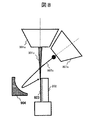
- FIG. 1 is a schematic configuration diagram of a charged particle beam apparatus according to a first embodiment of the present invention. It is a figure which shows an example which shows the track
- the present invention includes an electrode section for bending the trajectory of charged particles in a sample chamber of a charged particle beam apparatus including an ion beam column. And a charged particle beam is bent by the electric field which this electrode part generates, and a sample is irradiated.
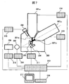
- FIG. 1 is an overall schematic configuration diagram of a charged particle beam apparatus to which a first embodiment of the present invention is applied.
- a charged particle beam apparatus is provided in an ion beam column 201a, a sample chamber 203, and a sample chamber 203, can be applied with voltage, can be moved in any direction, and an inclination angle is adjusted.
- the charged particle beam apparatus includes an ion beam scan controller 214 for controlling scanning of the ion beam 201b generated from the ion beam column 201a, and a detector 206 for obtaining a scanning ion microscope (SIM) image.
- a detector controller 215 that provides detected information to the integrated computer 213, a controller (keyboard, mouse, etc.) 216 for an operator to input various instructions such as irradiation conditions, electrode voltage conditions, and position conditions, and the acquired SIM
- a display 217 for displaying an image.
- the charged particle beam apparatus includes a current measuring device 207 for using the electrode unit 204 as a second detector, and a current measuring device control device 218 that performs processing such as amplification of the current value detected by the current measuring device 207. And. A current measurement signal from the current measuring device controller 218 is supplied to the integrated computer 213.
- the ion beam column 201a includes all components necessary for FIB, such as an ion source for generating the ion beam 201b, a lens for focusing the ion beam 201b, and a deflection system for scanning and shifting the ion beam. It is a system.
- the ion beam column 201 a is mounted in the sample chamber 203.
- gallium ions are generally used for the ion beam 201b, but any ion species may be used for processing purposes.
- the ion beam 201b is not limited to the focused ion beam, but may be a broad ion beam.
- one FIB column 201a is arranged, but two or more ion beam columns may be arranged.
- a configuration including a Ga focused ion beam column and an Ar focused ion beam column may be employed.
- the voltage supply device 205 that supplies a voltage to the electrode unit 204 can be modulated.
- Each controller can communicate with each other and is controlled by the integrated computer 213.
- one detector 206 for acquiring a SIM image is arranged, but a configuration including two or more identical or different detectors may be employed.
- a secondary electron detector and a secondary ion detector may be mounted.
- the sample chamber 203 is equipped with a sample stage, a gas deposition unit, a micro sampling unit, and the like.
- a sample stage 219 (shown in FIG. 2) for transporting the sample can place the sample 202, and can be moved, rotated, or tilted on a plane.
- the sample stage 219 can move a position necessary for ion beam processing and observation to an ion beam irradiation position.
- a gas deposition unit used for production of a protective film and marking can store a deposit gas that forms a deposited film by irradiation with a charged particle beam, and can supply the deposited gas from the tip of a nozzle as necessary.
- the microsampling unit that picks up a specific portion of the sample 202 by using the processing and cutting of the sample 202 by FIB includes a probe that can be moved in the sample chamber 203 by the probe driving unit.
- the probe is used to extract a minute sample piece formed on the sample 202 or to supply a potential to the sample by bringing it into contact with the sample surface.
- the detector controller 215 may include a circuit or an arithmetic processing unit that performs arithmetic processing on the detection signal from the detector 206 and images it.
- Each drive mechanism such as a sample stage, a deposition unit, and a micro sampling unit also has a control circuit. These control circuits can communicate with each other and are controlled in an integrated manner by one or more computers.
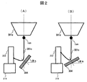
- FIG. 2 shows a case where the shape of the electrode of the electrode portion 204 is a flat plate electrode, and an ion beam (Ion) beam 301c from the tip portion 301a of the ion beam column 201a is applied by the flat plate electrode 304 to which a voltage is applied. Is bent, and the sample 202 supported by the sample stage 219 is irradiated.
- the position of the plate electrode 304 position along the extension line of the central axis of the ion beam column 201a, position in the direction orthogonal to the extension line of the central axis of the ion beam column 201a
- inclination angle ⁇ ion beam column
- FIG. 2A shows the case where the inclination angle is ⁇ A
- FIG. 2B shows the case where the inclination angle is ⁇ B.
- FIG. 3 shows a case where the electrode part 204 has a spherical electrode 404 in shape.
- the ion beam irradiation position and irradiation angle on the sample 202 can be changed.
- (A) in FIG. 3 is a case where the distance between the center of the extension line and the spherical electrodes 404 of the central axis of the ion beam column 201a is L A
- the distance L A is greater than L B.
- FIG. 4 shows a case where an electrode 504 having a parabolic shape (curved surface shape) is used as the electrode of the electrode unit 204. It is shown that by using this parabolic electrode 504, the spread of the irradiation position of the ion beam 301c can be suppressed.
- an electrode (a plurality of electrodes) composed of electrodes having the shapes shown in FIGS. 2, 3, and 4
- various irradiation positions and tilt angles can be changed by changing the position, inclination angle, and rotation angle of the electrodes.
- An irradiation angle can be realized.
- the irradiation position and the irradiation angle can also be changed by modulating the voltage applied to the electrode. That is, by combining the electrode shape, electrode voltage, electrode position, ion beam irradiation direction, and sample movement, a desired irradiation position can be irradiated with an ion beam at a desired irradiation angle.
- the sample surface can be irradiated with the ion beam at a wide range of angles. it can.
- the angle at which the ion beam 301c is extended from the central axis of the ion beam column 201a is changed by the electrode unit 204, and the electrode unit 204 is moved vertically and horizontally while maintaining the changed beam angle.
- the ion beam can be irradiated over one surface of the sample 202.
- a plurality of electrodes 604a (spherical electrodes) and 604b (plate electrodes) may be used simultaneously to realize a desired irradiation position and irradiation angle of the sample 202.
- the spherical electrode 604a (first electrode portion) can be positioned near the tip portion 301a of the ion beam column 201a
- the plate electrode 604b (second electrode portion) can be positioned near the sample 202.
- the support method of the electrode part 204 is not ask
- a unit for supporting an electrode may be newly prepared, or an electrode may be attached instead of a microsampling probe.
- the microsampling probe itself may be substituted for the electrode.
- the electrode unit 204 may be supported on one of the sample stages 219.
- an electrode unit for bending an ion trajectory 204 may be supported on the eucentric stage, and the sample may be supported on the (S) TEM common sample holder.
- the operation of the stage that supports the electrode unit 204 can be configured to be controlled by the electrode controller 211.
- a polyhedral electrode can be applied in addition to a flat plate electrode, a spherical electrode, and a parabolic electrode.
- the processing becomes non-uniform due to the difference in sputter rate, resulting in streaking in the cross section. For example, in a portion where heavy elements and light elements are alternately present in the upper part of the sample, the sputter rate of that portion is lowered, and a streak is formed in the processed cross section. This streak can be removed or reduced by arbitrarily changing the ion beam irradiation direction so that the sputtering rate is uniform.
- the ion beam can be irradiated from such an irradiation direction.
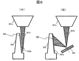
- FIG. 6A shows a method for removing a damaged layer when the present invention is not adopted.
- a damaged layer 721 is formed on the sample 202 by ion beam irradiation.
- the ion beam 301b used for removing the damaged layer 721 is an ion beam 301b irradiated from the same direction as the main processing beam. Therefore, as shown in FIG. 6A, the damage layer 721 is removed using a part of the ion beam 301b (a part of the side of the ion beam 301b). Therefore, it is very inefficient.
- the surface 202a of the sample 202 is processed by the ion beam 301b with the plate electrode 304 moved from the illustrated position. Thereafter, the sample 202 is moved, the plate electrode 304 is moved to the illustrated position, the ion beam 301b is bent by the plate electrode 304, and the damage layer 721 is irradiated, so that the ion beam 301b can be used without waste. The damaged layer 721 can be removed efficiently.
- the position and inclination of the electrode 304 can be adjusted together.
- (S) TEM thin film sample preparation as shown in Patent Document 4, in order to obtain a vertical processing cross section, a method of irradiating an ion beam while tilting the sample is taken. If the orientation can be arbitrarily selected, a vertical processed cross section can be obtained without tilting the sample. Furthermore, by irradiating the ion beam from below, the thickened portion (bottom portion) of the thin film sample can be intensively removed, which is efficient.
- the point that the ion beam can be irradiated from an arbitrary direction is a great advantage also on the observation surface.
- SIM images from various directions can be acquired even on a sample stage that does not have an inclination mechanism or a rotation mechanism.
- the current reaching the electrode unit 204 is measured using the current measuring device 207, and the measured current signal is supplied to the integrated computer 213 via the current measuring device control device 218. Then, the integrated computer 213 acquires a SIM image based on the current signal supplied from the current measuring device controller 218. Therefore, a SIM image can be acquired even when the electrode 204 is arranged in the vicinity of the sample 202.
- the electrode 204 to which a negative voltage is applied is arranged in the vicinity of the sample 202, the same can be said for the secondary ions emitted from the sample 202.
- the moving distance of the ion beam can be extended.
- the scanable range of the ion beam depends on the distance from the emission of the ion beam column 201a to the arrival of the sample 202, and the observation region becomes wider as the distance becomes longer.
- the scanning range of the focused ion beam can be expanded. That is, the observable range at a low magnification can be expanded. This is advantageous when searching for a visual field. It can also be used when processing a wider range.
- the position in the direction along the extension of the central axis of the ion beam column 201a, the position in the orthogonal direction, and the inclination angle ⁇ (the central axis of the ion beam column 201a).
- An electrode 204 such as an electrode 304, 404, 504 or the like that can be adjusted) is arranged in the sample chamber 203, and the ion beam 301 c bent by the electrode 304 or the like is applied to the sample 202.
- the first embodiment of the present invention it is possible to provide an apparatus capable of efficiently removing a damage layer and surface roughness formed on an ion beam irradiation surface during FIB processing.
- the distance until the ion beam emitted from the ion beam column 201a reaches the sample surface can be extended, and the scanning range can be expanded to expand the low magnification observation range.
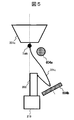
- FIG. 7 is a schematic configuration diagram of the entire charged particle beam apparatus to which the second embodiment of the present invention is applied.
- the charged particle beam apparatus includes an SEM column 807a and an electron beam scan controller for controlling scanning of the electron beam 807b of the SEM column 807a in addition to the apparatus configuration of the first embodiment. 818, and the other configuration is the same as that of the first embodiment.
- the SEM column 807a includes all components necessary for the SEM, such as an electron source for generating an electron beam, a lens for focusing the electron beam, and a deflection system for scanning and shifting the electron beam. It is a system.
- the charged particle beam apparatus according to the second embodiment of the present invention is an apparatus capable of SEM observation of the cross section of the sample 202 subjected to FIB processing on the spot.
- the ion beam column 201a is vertically arranged and the SEM column 807a is inclined.
- the present invention is not limited thereto, and the ion beam column 201a is inclined and the SEM column 807a is arranged. It may be arranged vertically. Further, both the ion beam column 201a and the SEM column 807a may be inclined.
- a triple column configuration including a Ga focused ion beam column, an Ar focused ion beam column, and an electron beam column may be employed.
- a detector for obtaining an SEM image, a detector controller for providing detected information to the integrated computer, and an SEM image generated based on the detection signal are displayed.
- the display is configured to be the same as that for the SIM image, but may include one or a plurality of detectors, a detector controller, and a display as a mechanism for acquiring and displaying the SEM image.
- the processing state of the ion beam 201b is observed from various directions by SEM observation by bending the electron trajectory and irradiating the sample 202. be able to.
- the processing state can be observed by SEM by irradiating the front side surface of the sample 202 with an electron beam 807b from the SEM column 807a.
- the parabolic electrode 904 is bent at the trajectory of the electron beam 807c from the SEM column 807a, and the position irradiated with the ion beam 301c emitted from the tip 301a of the ion beam column 201a is irradiated. It arrange
- the acceleration voltage of the ion beam 301c is higher than the acceleration voltage of the electron beam 807c.
- the acceleration voltage of the electron beam 807b is set higher than the acceleration voltage of the ion beam 201b. Is preferable. By doing so, it is possible to realize SEM observation during ion beam processing with little influence on the electron beam 807b.
- the moving distance of the electron beam 807b can be extended. Therefore, similarly to the case of the SIM observation, it is possible to enlarge the observable range at a low magnification even in the SEM observation.
- the same effect as that of the first embodiment can be obtained, and as described above, the desired position of the sample surface during processing by the ion beam can be observed by the SEM. Can do.
- the electric field is used to change the trajectory of the charged particles.
- the trajectory of the charged particles can be changed using a magnetic field.
- the charged particle trajectory can be changed by installing a coil or permanent magnet in the sample chamber.
- the FIB-SEM apparatus provides an apparatus that can observe not only the front surface of the sample but also the back surface thereof.
- both sides can be observed without moving the sample, and the processing accuracy and processing reproducibility of the thin film sample are dramatically improved.
- 201a ion beam column, 201b, 301b, 301c: ion beam, 202: sample, 202a: sample surface, 203: sample chamber, 204: electrode unit, 205: voltage supply device, 206: detector, 207: current measuring device 211: electrode controller, 212: voltage controller, 213: integrated computer, 214: ion beam scan controller, 215: controller for detector, 216: controller, 217: display, 218: controller for current measuring device, 219: Sample stage, 721: Damaged layer, 301a: Tip of ion beam column, 304, 604b: Plate electrode, 404, 604a: Spherical electrode, 504, 904: Parabolic electrode, 807a: Scanning electron microscope column, 807b: Electron Beam, 807c: electron beam, 818: electron beam scan Down controller, 923: sample back surface
Landscapes
- Chemical & Material Sciences (AREA)
- Analytical Chemistry (AREA)
- Analysing Materials By The Use Of Radiation (AREA)
- Sampling And Sample Adjustment (AREA)
Priority Applications (2)
| Application Number | Priority Date | Filing Date | Title |
|---|---|---|---|
| US13/991,678 US20130248733A1 (en) | 2010-12-06 | 2011-11-30 | Charged particle beam apparatus and method of irradiating charged particle beam |
| EP11847394.1A EP2650901A1 (en) | 2010-12-06 | 2011-11-30 | Charged particle beam apparatus and method of irradiating charged particle beam |
Applications Claiming Priority (2)
| Application Number | Priority Date | Filing Date | Title |
|---|---|---|---|
| JP2010271806A JP5489295B2 (ja) | 2010-12-06 | 2010-12-06 | 荷電粒子線装置及び荷電粒子線照射方法 |
| JP2010-271806 | 2010-12-06 |
Publications (1)
| Publication Number | Publication Date |
|---|---|
| WO2012077554A1 true WO2012077554A1 (ja) | 2012-06-14 |
Family
ID=46207044
Family Applications (1)
| Application Number | Title | Priority Date | Filing Date |
|---|---|---|---|
| PCT/JP2011/077670 Ceased WO2012077554A1 (ja) | 2010-12-06 | 2011-11-30 | 荷電粒子線装置及び荷電粒子線照射方法 |
Country Status (4)
| Country | Link |
|---|---|
| US (1) | US20130248733A1 (enExample) |
| EP (1) | EP2650901A1 (enExample) |
| JP (1) | JP5489295B2 (enExample) |
| WO (1) | WO2012077554A1 (enExample) |
Families Citing this family (3)
| Publication number | Priority date | Publication date | Assignee | Title |
|---|---|---|---|---|
| JP6108674B2 (ja) * | 2012-03-16 | 2017-04-05 | 株式会社日立ハイテクサイエンス | 荷電粒子ビーム装置及び試料搬送装置 |
| US10062546B2 (en) * | 2013-05-14 | 2018-08-28 | Hitachi, Ltd. | Sample holder and focused-ion-beam machining device provided therewith |
| US10388489B2 (en) * | 2017-02-07 | 2019-08-20 | Kla-Tencor Corporation | Electron source architecture for a scanning electron microscopy system |
Citations (12)
| Publication number | Priority date | Publication date | Assignee | Title |
|---|---|---|---|---|
| JPH03101849U (enExample) * | 1990-02-02 | 1991-10-23 | ||
| JPH085528A (ja) | 1994-06-23 | 1996-01-12 | Sharp Corp | 透過電子顕微鏡用断面試料作成用集束イオンビーム装置及び透過電子顕微鏡用断面試料作成方法 |
| JP2002117796A (ja) * | 2000-10-11 | 2002-04-19 | Jeol Ltd | 荷電粒子ビーム装置および集束イオンビーム装置 |
| JP2002148159A (ja) | 2000-11-06 | 2002-05-22 | Hitachi Ltd | 試料作製方法および試料作製装置 |
| JP2002277364A (ja) | 2001-03-19 | 2002-09-25 | Seiko Epson Corp | 薄片試料加工方法及び薄片試料の作製方法 |
| JP2003513419A (ja) * | 1999-10-22 | 2003-04-08 | バリアン・セミコンダクター・エクイップメント・アソシエイツ・インコーポレイテッド | 広いダイナミックレンジのイオンビームスキャナー |
| JP2003528659A (ja) * | 2000-03-07 | 2003-09-30 | ジー エス アイ ゲゼルシャフト フュア シュベールイオーネンフォルシュンク エム ベー ハー | 腫瘍組織を照射するためのイオンビームシステム |
| JP2004264145A (ja) | 2003-02-28 | 2004-09-24 | Toshiba Corp | 透過型電子顕微鏡観察試料の作製方法 |
| JP2004362829A (ja) * | 2003-06-02 | 2004-12-24 | Hitachi High-Technologies Corp | 荷電粒子線装置 |
| JP2006032154A (ja) * | 2004-07-16 | 2006-02-02 | Hiroyuki Noguchi | 集束イオンビーム加工方法および集束イオンビーム加工装置 |
| JP2007193977A (ja) | 2006-01-17 | 2007-08-02 | Hitachi High-Technologies Corp | 荷電ビーム装置及び荷電ビーム加工方法 |
| JP2011146690A (ja) * | 2009-12-18 | 2011-07-28 | Canon Anelva Corp | イオンビーム発生装置及びこれを用いた基板処理装置と電子デバイス製造方法 |
Family Cites Families (6)
| Publication number | Priority date | Publication date | Assignee | Title |
|---|---|---|---|---|
| US4096386A (en) * | 1977-04-04 | 1978-06-20 | Taylor-Kincaid Company | Light reflecting electrostatic electron lens |
| DE3525994A1 (de) * | 1985-07-20 | 1987-01-29 | Philips Patentverwaltung | Elektronenstrahl-aufzeichnungstraeger |
| JPH0734871B2 (ja) * | 1989-09-14 | 1995-04-19 | 株式会社クボタ | 精米機 |
| JP2007012516A (ja) * | 2005-07-01 | 2007-01-18 | Jeol Ltd | 荷電粒子ビーム装置及び荷電粒子ビームを用いた試料情報検出方法 |
| JP5016988B2 (ja) * | 2007-06-19 | 2012-09-05 | 株式会社日立ハイテクノロジーズ | 荷電粒子線装置およびその真空立上げ方法 |
| JP4901696B2 (ja) * | 2007-11-06 | 2012-03-21 | キヤノンアネルバ株式会社 | 成膜装置 |
-
2010
- 2010-12-06 JP JP2010271806A patent/JP5489295B2/ja not_active Expired - Fee Related
-
2011
- 2011-11-30 WO PCT/JP2011/077670 patent/WO2012077554A1/ja not_active Ceased
- 2011-11-30 US US13/991,678 patent/US20130248733A1/en not_active Abandoned
- 2011-11-30 EP EP11847394.1A patent/EP2650901A1/en not_active Withdrawn
Patent Citations (12)
| Publication number | Priority date | Publication date | Assignee | Title |
|---|---|---|---|---|
| JPH03101849U (enExample) * | 1990-02-02 | 1991-10-23 | ||
| JPH085528A (ja) | 1994-06-23 | 1996-01-12 | Sharp Corp | 透過電子顕微鏡用断面試料作成用集束イオンビーム装置及び透過電子顕微鏡用断面試料作成方法 |
| JP2003513419A (ja) * | 1999-10-22 | 2003-04-08 | バリアン・セミコンダクター・エクイップメント・アソシエイツ・インコーポレイテッド | 広いダイナミックレンジのイオンビームスキャナー |
| JP2003528659A (ja) * | 2000-03-07 | 2003-09-30 | ジー エス アイ ゲゼルシャフト フュア シュベールイオーネンフォルシュンク エム ベー ハー | 腫瘍組織を照射するためのイオンビームシステム |
| JP2002117796A (ja) * | 2000-10-11 | 2002-04-19 | Jeol Ltd | 荷電粒子ビーム装置および集束イオンビーム装置 |
| JP2002148159A (ja) | 2000-11-06 | 2002-05-22 | Hitachi Ltd | 試料作製方法および試料作製装置 |
| JP2002277364A (ja) | 2001-03-19 | 2002-09-25 | Seiko Epson Corp | 薄片試料加工方法及び薄片試料の作製方法 |
| JP2004264145A (ja) | 2003-02-28 | 2004-09-24 | Toshiba Corp | 透過型電子顕微鏡観察試料の作製方法 |
| JP2004362829A (ja) * | 2003-06-02 | 2004-12-24 | Hitachi High-Technologies Corp | 荷電粒子線装置 |
| JP2006032154A (ja) * | 2004-07-16 | 2006-02-02 | Hiroyuki Noguchi | 集束イオンビーム加工方法および集束イオンビーム加工装置 |
| JP2007193977A (ja) | 2006-01-17 | 2007-08-02 | Hitachi High-Technologies Corp | 荷電ビーム装置及び荷電ビーム加工方法 |
| JP2011146690A (ja) * | 2009-12-18 | 2011-07-28 | Canon Anelva Corp | イオンビーム発生装置及びこれを用いた基板処理装置と電子デバイス製造方法 |
Also Published As
| Publication number | Publication date |
|---|---|
| US20130248733A1 (en) | 2013-09-26 |
| JP2012123942A (ja) | 2012-06-28 |
| JP5489295B2 (ja) | 2014-05-14 |
| EP2650901A1 (en) | 2013-10-16 |
Similar Documents
| Publication | Publication Date | Title |
|---|---|---|
| CN107084869B (zh) | 用于横截面视图薄层的背侧打薄的高吞吐量tem制备工艺和硬件 | |
| JP6586261B2 (ja) | 大容量temグリッド及び試料取り付け方法 | |
| CN103403520A (zh) | Tem样品制备 | |
| TWI813760B (zh) | 試料加工觀察方法 | |
| TWI768001B (zh) | 帶電粒子束裝置以及試樣加工方法 | |
| CN104251795B (zh) | 平面视图样品制备 | |
| JP5323405B2 (ja) | Tem試料作製方法、及びtem試料 | |
| JP5489295B2 (ja) | 荷電粒子線装置及び荷電粒子線照射方法 | |
| KR101539738B1 (ko) | 주사전자 현미경 | |
| CN109841534A (zh) | 截面加工观察方法、带电粒子束装置 | |
| JP2009037910A (ja) | 複合荷電粒子ビーム装置及び加工観察方法 | |
| US11199480B2 (en) | Thin-sample-piece fabricating device and thin-sample-piece fabricating method | |
| US11094503B2 (en) | Method of preparing thin film sample piece and charged particle beam apparatus | |
| JP7578848B2 (ja) | 荷電粒子ビーム装置、及び荷電粒子ビーム装置の制御方法 | |
| JP7214262B2 (ja) | 荷電粒子ビーム装置、試料加工方法 | |
| JP7622248B2 (ja) | 荷電粒子ビーム装置、及び荷電粒子ビーム装置の制御方法 | |
| WO2024171388A1 (ja) | 荷電粒子ビーム装置、及び荷電粒子ビーム装置の制御方法 | |
| US20240055220A1 (en) | Charged Particle Beam Device |
Legal Events
| Date | Code | Title | Description |
|---|---|---|---|
| 121 | Ep: the epo has been informed by wipo that ep was designated in this application |
Ref document number: 11847394 Country of ref document: EP Kind code of ref document: A1 |
|
| WWE | Wipo information: entry into national phase |
Ref document number: 13991678 Country of ref document: US |
|
| NENP | Non-entry into the national phase |
Ref country code: DE |
|
| WWE | Wipo information: entry into national phase |
Ref document number: 2011847394 Country of ref document: EP |