WO2012077554A1 - Charged particle beam apparatus and method of irradiating charged particle beam - Google Patents
Charged particle beam apparatus and method of irradiating charged particle beam Download PDFInfo
- Publication number
- WO2012077554A1 WO2012077554A1 PCT/JP2011/077670 JP2011077670W WO2012077554A1 WO 2012077554 A1 WO2012077554 A1 WO 2012077554A1 JP 2011077670 W JP2011077670 W JP 2011077670W WO 2012077554 A1 WO2012077554 A1 WO 2012077554A1
- Authority
- WO
- WIPO (PCT)
- Prior art keywords
- sample
- charged particle
- particle beam
- ion beam
- electrode
- Prior art date
Links
Images


Classifications
-
- H—ELECTRICITY
- H01—ELECTRIC ELEMENTS
- H01J—ELECTRIC DISCHARGE TUBES OR DISCHARGE LAMPS
- H01J37/00—Discharge tubes with provision for introducing objects or material to be exposed to the discharge, e.g. for the purpose of examination or processing thereof
- H01J37/02—Details
- H01J37/04—Arrangements of electrodes and associated parts for generating or controlling the discharge, e.g. electron-optical arrangement, ion-optical arrangement
- H01J37/147—Arrangements for directing or deflecting the discharge along a desired path
-
- H—ELECTRICITY
- H01—ELECTRIC ELEMENTS
- H01J—ELECTRIC DISCHARGE TUBES OR DISCHARGE LAMPS
- H01J29/00—Details of cathode-ray tubes or of electron-beam tubes of the types covered by group H01J31/00
- H01J29/46—Arrangements of electrodes and associated parts for generating or controlling the ray or beam, e.g. electron-optical arrangement
- H01J29/70—Arrangements for deflecting ray or beam
-
- H—ELECTRICITY
- H01—ELECTRIC ELEMENTS
- H01J—ELECTRIC DISCHARGE TUBES OR DISCHARGE LAMPS
- H01J37/00—Discharge tubes with provision for introducing objects or material to be exposed to the discharge, e.g. for the purpose of examination or processing thereof
- H01J37/02—Details
- H01J37/023—Means for mechanically adjusting components not otherwise provided for
-
- H—ELECTRICITY
- H01—ELECTRIC ELEMENTS
- H01J—ELECTRIC DISCHARGE TUBES OR DISCHARGE LAMPS
- H01J37/00—Discharge tubes with provision for introducing objects or material to be exposed to the discharge, e.g. for the purpose of examination or processing thereof
- H01J37/30—Electron-beam or ion-beam tubes for localised treatment of objects
- H01J37/317—Electron-beam or ion-beam tubes for localised treatment of objects for changing properties of the objects or for applying thin layers thereon, e.g. for ion implantation
-
- H—ELECTRICITY
- H01—ELECTRIC ELEMENTS
- H01J—ELECTRIC DISCHARGE TUBES OR DISCHARGE LAMPS
- H01J2237/00—Discharge tubes exposing object to beam, e.g. for analysis treatment, etching, imaging
- H01J2237/03—Mounting, supporting, spacing or insulating electrodes
Definitions
- the present invention relates to a charged particle beam apparatus and a charged particle beam irradiation method using an ion beam, for example.
- a focused ion beam (FIB) apparatus has been used for preparing a thin film sample for observation with a (scanning) transmission electron microscope ((S) TEM).
- the FIB apparatus has become an indispensable tool in the preparation of thin film samples for semiconductor device failure analysis.
- Patent Document 1 discloses a method in which a second ion beam (argon ion) different from the first ion beam (gallium ion) used for thin film processing is used for removing the damaged layer. Yes.
- Patent Document 2 discloses a method for removing a damaged layer by irradiating a thin sample with argon ions using an ion milling apparatus.
- Patent Document 3 discloses a method for reducing the energy of the ion beam used for the finishing process to be lower than the energy of the ion beam used for the main process in order to reduce the damage layer.
- a decrease in throughput can be suppressed by performing a finishing process by tilting a sample with reference to an ion beam.
- Patent Document 4 discloses a method for obtaining a vertical cross section by inclining a sample by a predetermined angle and irradiating an ion beam. In general, processing is performed by inclining the sample surface by an angle of about 3 to 5 degrees with respect to the central axis of the ion beam.
- Patent Document 5 describes a technique capable of changing the angle of the ion beam with respect to the sample surface from 75 degrees to 90 degrees using an angle changing electrode.
- Patent Documents 1 to 3 have a great restriction on the irradiation direction of the ion beam. For this reason, it is difficult to irradiate only a desired region of the sample with an ion beam or to irradiate at an optimum angle.
- the angle of the ion beam with respect to the sample surface can be changed, but the sample cannot be irradiated with the ion beam at an angle larger than that, and a desired angle can be applied to a desired region. It is difficult to irradiate with.
- An object of the present invention is to realize a charged particle beam apparatus and a charged particle beam irradiation method capable of irradiating a desired region with a wide range of angles with respect to a sample surface with respect to a sample surface.
- the charged particle beam device includes an ion beam column, a sample chamber to which the ion beam column is attached, a sample stage disposed in the sample chamber, a sample chamber, a trajectory of the ion beam, and a sample An electrode unit for irradiating the sample supported by the stage and an electrode unit movement control unit for moving the electrode unit are provided.
- the trajectory of the ion beam generated from the ion beam column can change the angle formed with the extension of the central axis of the ion beam column by the electrode unit, and irradiate the sample supported by the sample stage with the ion beam. it can.
- a charged particle beam apparatus and a charged particle beam irradiation method that can irradiate a desired region with a wide range of angles with respect to a sample surface with respect to a sample surface can be realized.
- FIG. 1 is a schematic configuration diagram of a charged particle beam apparatus according to a first embodiment of the present invention. It is a figure which shows an example which shows the track
- the present invention includes an electrode section for bending the trajectory of charged particles in a sample chamber of a charged particle beam apparatus including an ion beam column. And a charged particle beam is bent by the electric field which this electrode part generates, and a sample is irradiated.
- FIG. 1 is an overall schematic configuration diagram of a charged particle beam apparatus to which a first embodiment of the present invention is applied.
- a charged particle beam apparatus is provided in an ion beam column 201a, a sample chamber 203, and a sample chamber 203, can be applied with voltage, can be moved in any direction, and an inclination angle is adjusted.
- the charged particle beam apparatus includes an ion beam scan controller 214 for controlling scanning of the ion beam 201b generated from the ion beam column 201a, and a detector 206 for obtaining a scanning ion microscope (SIM) image.
- a detector controller 215 that provides detected information to the integrated computer 213, a controller (keyboard, mouse, etc.) 216 for an operator to input various instructions such as irradiation conditions, electrode voltage conditions, and position conditions, and the acquired SIM
- a display 217 for displaying an image.
- the charged particle beam apparatus includes a current measuring device 207 for using the electrode unit 204 as a second detector, and a current measuring device control device 218 that performs processing such as amplification of the current value detected by the current measuring device 207. And. A current measurement signal from the current measuring device controller 218 is supplied to the integrated computer 213.
- the ion beam column 201a includes all components necessary for FIB, such as an ion source for generating the ion beam 201b, a lens for focusing the ion beam 201b, and a deflection system for scanning and shifting the ion beam. It is a system.
- the ion beam column 201 a is mounted in the sample chamber 203.
- gallium ions are generally used for the ion beam 201b, but any ion species may be used for processing purposes.
- the ion beam 201b is not limited to the focused ion beam, but may be a broad ion beam.
- one FIB column 201a is arranged, but two or more ion beam columns may be arranged.
- a configuration including a Ga focused ion beam column and an Ar focused ion beam column may be employed.
- the voltage supply device 205 that supplies a voltage to the electrode unit 204 can be modulated.
- Each controller can communicate with each other and is controlled by the integrated computer 213.
- one detector 206 for acquiring a SIM image is arranged, but a configuration including two or more identical or different detectors may be employed.
- a secondary electron detector and a secondary ion detector may be mounted.
- the sample chamber 203 is equipped with a sample stage, a gas deposition unit, a micro sampling unit, and the like.
- a sample stage 219 (shown in FIG. 2) for transporting the sample can place the sample 202, and can be moved, rotated, or tilted on a plane.
- the sample stage 219 can move a position necessary for ion beam processing and observation to an ion beam irradiation position.
- a gas deposition unit used for production of a protective film and marking can store a deposit gas that forms a deposited film by irradiation with a charged particle beam, and can supply the deposited gas from the tip of a nozzle as necessary.
- the microsampling unit that picks up a specific portion of the sample 202 by using the processing and cutting of the sample 202 by FIB includes a probe that can be moved in the sample chamber 203 by the probe driving unit.
- the probe is used to extract a minute sample piece formed on the sample 202 or to supply a potential to the sample by bringing it into contact with the sample surface.
- the detector controller 215 may include a circuit or an arithmetic processing unit that performs arithmetic processing on the detection signal from the detector 206 and images it.
- Each drive mechanism such as a sample stage, a deposition unit, and a micro sampling unit also has a control circuit. These control circuits can communicate with each other and are controlled in an integrated manner by one or more computers.
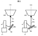
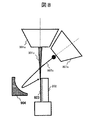
- FIG. 2 shows a case where the shape of the electrode of the electrode portion 204 is a flat plate electrode, and an ion beam (Ion) beam 301c from the tip portion 301a of the ion beam column 201a is applied by the flat plate electrode 304 to which a voltage is applied. Is bent, and the sample 202 supported by the sample stage 219 is irradiated.
- the position of the plate electrode 304 position along the extension line of the central axis of the ion beam column 201a, position in the direction orthogonal to the extension line of the central axis of the ion beam column 201a
- inclination angle ⁇ ion beam column
- FIG. 2A shows the case where the inclination angle is ⁇ A
- FIG. 2B shows the case where the inclination angle is ⁇ B.
- FIG. 3 shows a case where the electrode part 204 has a spherical electrode 404 in shape.
- the ion beam irradiation position and irradiation angle on the sample 202 can be changed.
- (A) in FIG. 3 is a case where the distance between the center of the extension line and the spherical electrodes 404 of the central axis of the ion beam column 201a is L A
- the distance L A is greater than L B.
- FIG. 4 shows a case where an electrode 504 having a parabolic shape (curved surface shape) is used as the electrode of the electrode unit 204. It is shown that by using this parabolic electrode 504, the spread of the irradiation position of the ion beam 301c can be suppressed.
- an electrode (a plurality of electrodes) composed of electrodes having the shapes shown in FIGS. 2, 3, and 4
- various irradiation positions and tilt angles can be changed by changing the position, inclination angle, and rotation angle of the electrodes.
- An irradiation angle can be realized.
- the irradiation position and the irradiation angle can also be changed by modulating the voltage applied to the electrode. That is, by combining the electrode shape, electrode voltage, electrode position, ion beam irradiation direction, and sample movement, a desired irradiation position can be irradiated with an ion beam at a desired irradiation angle.
- the sample surface can be irradiated with the ion beam at a wide range of angles. it can.
- the angle at which the ion beam 301c is extended from the central axis of the ion beam column 201a is changed by the electrode unit 204, and the electrode unit 204 is moved vertically and horizontally while maintaining the changed beam angle.
- the ion beam can be irradiated over one surface of the sample 202.
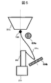
- a plurality of electrodes 604a (spherical electrodes) and 604b (plate electrodes) may be used simultaneously to realize a desired irradiation position and irradiation angle of the sample 202.
- the spherical electrode 604a (first electrode portion) can be positioned near the tip portion 301a of the ion beam column 201a
- the plate electrode 604b (second electrode portion) can be positioned near the sample 202.
- the support method of the electrode part 204 is not ask
- a unit for supporting an electrode may be newly prepared, or an electrode may be attached instead of a microsampling probe.
- the microsampling probe itself may be substituted for the electrode.
- the electrode unit 204 may be supported on one of the sample stages 219.
- an electrode unit for bending an ion trajectory 204 may be supported on the eucentric stage, and the sample may be supported on the (S) TEM common sample holder.
- the operation of the stage that supports the electrode unit 204 can be configured to be controlled by the electrode controller 211.
- a polyhedral electrode can be applied in addition to a flat plate electrode, a spherical electrode, and a parabolic electrode.
- the processing becomes non-uniform due to the difference in sputter rate, resulting in streaking in the cross section. For example, in a portion where heavy elements and light elements are alternately present in the upper part of the sample, the sputter rate of that portion is lowered, and a streak is formed in the processed cross section. This streak can be removed or reduced by arbitrarily changing the ion beam irradiation direction so that the sputtering rate is uniform.
- the ion beam can be irradiated from such an irradiation direction.
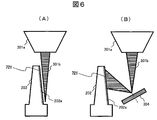
- FIG. 6A shows a method for removing a damaged layer when the present invention is not adopted.
- a damaged layer 721 is formed on the sample 202 by ion beam irradiation.
- the ion beam 301b used for removing the damaged layer 721 is an ion beam 301b irradiated from the same direction as the main processing beam. Therefore, as shown in FIG. 6A, the damage layer 721 is removed using a part of the ion beam 301b (a part of the side of the ion beam 301b). Therefore, it is very inefficient.
- the surface 202a of the sample 202 is processed by the ion beam 301b with the plate electrode 304 moved from the illustrated position. Thereafter, the sample 202 is moved, the plate electrode 304 is moved to the illustrated position, the ion beam 301b is bent by the plate electrode 304, and the damage layer 721 is irradiated, so that the ion beam 301b can be used without waste. The damaged layer 721 can be removed efficiently.
- the position and inclination of the electrode 304 can be adjusted together.
- (S) TEM thin film sample preparation as shown in Patent Document 4, in order to obtain a vertical processing cross section, a method of irradiating an ion beam while tilting the sample is taken. If the orientation can be arbitrarily selected, a vertical processed cross section can be obtained without tilting the sample. Furthermore, by irradiating the ion beam from below, the thickened portion (bottom portion) of the thin film sample can be intensively removed, which is efficient.
- the point that the ion beam can be irradiated from an arbitrary direction is a great advantage also on the observation surface.
- SIM images from various directions can be acquired even on a sample stage that does not have an inclination mechanism or a rotation mechanism.
- the current reaching the electrode unit 204 is measured using the current measuring device 207, and the measured current signal is supplied to the integrated computer 213 via the current measuring device control device 218. Then, the integrated computer 213 acquires a SIM image based on the current signal supplied from the current measuring device controller 218. Therefore, a SIM image can be acquired even when the electrode 204 is arranged in the vicinity of the sample 202.
- the electrode 204 to which a negative voltage is applied is arranged in the vicinity of the sample 202, the same can be said for the secondary ions emitted from the sample 202.
- the moving distance of the ion beam can be extended.
- the scanable range of the ion beam depends on the distance from the emission of the ion beam column 201a to the arrival of the sample 202, and the observation region becomes wider as the distance becomes longer.
- the scanning range of the focused ion beam can be expanded. That is, the observable range at a low magnification can be expanded. This is advantageous when searching for a visual field. It can also be used when processing a wider range.
- the position in the direction along the extension of the central axis of the ion beam column 201a, the position in the orthogonal direction, and the inclination angle ⁇ (the central axis of the ion beam column 201a).
- An electrode 204 such as an electrode 304, 404, 504 or the like that can be adjusted) is arranged in the sample chamber 203, and the ion beam 301 c bent by the electrode 304 or the like is applied to the sample 202.
- the first embodiment of the present invention it is possible to provide an apparatus capable of efficiently removing a damage layer and surface roughness formed on an ion beam irradiation surface during FIB processing.
- the distance until the ion beam emitted from the ion beam column 201a reaches the sample surface can be extended, and the scanning range can be expanded to expand the low magnification observation range.
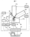
- FIG. 7 is a schematic configuration diagram of the entire charged particle beam apparatus to which the second embodiment of the present invention is applied.
- the charged particle beam apparatus includes an SEM column 807a and an electron beam scan controller for controlling scanning of the electron beam 807b of the SEM column 807a in addition to the apparatus configuration of the first embodiment. 818, and the other configuration is the same as that of the first embodiment.
- the SEM column 807a includes all components necessary for the SEM, such as an electron source for generating an electron beam, a lens for focusing the electron beam, and a deflection system for scanning and shifting the electron beam. It is a system.
- the charged particle beam apparatus according to the second embodiment of the present invention is an apparatus capable of SEM observation of the cross section of the sample 202 subjected to FIB processing on the spot.
- the ion beam column 201a is vertically arranged and the SEM column 807a is inclined.
- the present invention is not limited thereto, and the ion beam column 201a is inclined and the SEM column 807a is arranged. It may be arranged vertically. Further, both the ion beam column 201a and the SEM column 807a may be inclined.
- a triple column configuration including a Ga focused ion beam column, an Ar focused ion beam column, and an electron beam column may be employed.
- a detector for obtaining an SEM image, a detector controller for providing detected information to the integrated computer, and an SEM image generated based on the detection signal are displayed.
- the display is configured to be the same as that for the SIM image, but may include one or a plurality of detectors, a detector controller, and a display as a mechanism for acquiring and displaying the SEM image.
- the processing state of the ion beam 201b is observed from various directions by SEM observation by bending the electron trajectory and irradiating the sample 202. be able to.
- the processing state can be observed by SEM by irradiating the front side surface of the sample 202 with an electron beam 807b from the SEM column 807a.
- the parabolic electrode 904 is bent at the trajectory of the electron beam 807c from the SEM column 807a, and the position irradiated with the ion beam 301c emitted from the tip 301a of the ion beam column 201a is irradiated. It arrange
- the acceleration voltage of the ion beam 301c is higher than the acceleration voltage of the electron beam 807c.
- the acceleration voltage of the electron beam 807b is set higher than the acceleration voltage of the ion beam 201b. Is preferable. By doing so, it is possible to realize SEM observation during ion beam processing with little influence on the electron beam 807b.
- the moving distance of the electron beam 807b can be extended. Therefore, similarly to the case of the SIM observation, it is possible to enlarge the observable range at a low magnification even in the SEM observation.
- the same effect as that of the first embodiment can be obtained, and as described above, the desired position of the sample surface during processing by the ion beam can be observed by the SEM. Can do.
- the electric field is used to change the trajectory of the charged particles.
- the trajectory of the charged particles can be changed using a magnetic field.
- the charged particle trajectory can be changed by installing a coil or permanent magnet in the sample chamber.
- the FIB-SEM apparatus provides an apparatus that can observe not only the front surface of the sample but also the back surface thereof.
- both sides can be observed without moving the sample, and the processing accuracy and processing reproducibility of the thin film sample are dramatically improved.
- 201a ion beam column, 201b, 301b, 301c: ion beam, 202: sample, 202a: sample surface, 203: sample chamber, 204: electrode unit, 205: voltage supply device, 206: detector, 207: current measuring device 211: electrode controller, 212: voltage controller, 213: integrated computer, 214: ion beam scan controller, 215: controller for detector, 216: controller, 217: display, 218: controller for current measuring device, 219: Sample stage, 721: Damaged layer, 301a: Tip of ion beam column, 304, 604b: Plate electrode, 404, 604a: Spherical electrode, 504, 904: Parabolic electrode, 807a: Scanning electron microscope column, 807b: Electron Beam, 807c: electron beam, 818: electron beam scan Down controller, 923: sample back surface
Abstract
In order to provide a charged particle beam apparatus capable of irradiating a desired region in the surface of a sample with a charged particle beam from a wide range of angles, an electrode unit (204) comprising an electrode, the inclination angle of which (i.e. the angle of inclination relative to a plane orthogonal to the extension line of the center axis of the ion beam column (201a)) and the position of which (i.e. the position in the direction along the extension line of the center axis of the ion beam column (201a) and in directions orthogonal thereto) can be adjusted, is arranged within a sample chamber (203) of the charged particle beam apparatus. The charged particle beam apparatus is also configured so that a curved ion beam (201b) is irradiated onto a surface of a sample (202) by the electrode. This enables irradiation of the ion beam (201b) to a desired range within the surface of the sample (202), from a wide range of angles with respect to the sample surface.
Description
本発明は、例えば、イオンビームを用いる荷電粒子線装置及び荷電粒子線照射方法に関する。
The present invention relates to a charged particle beam apparatus and a charged particle beam irradiation method using an ion beam, for example.
近年、(走査)透過電子顕微鏡((S)TEM)観察用の薄膜試料作製には、集束イオンビーム(FIB)装置が用いられている。特に、半導体デバイス不良解析用の薄膜試料作製において、FIB装置は必須のツールとなっている。
In recent years, a focused ion beam (FIB) apparatus has been used for preparing a thin film sample for observation with a (scanning) transmission electron microscope ((S) TEM). In particular, the FIB apparatus has become an indispensable tool in the preparation of thin film samples for semiconductor device failure analysis.
近年、半導体産業を筆頭に、燃料電池や太陽電池といったエネルギー産業や、有機エレクトロルミネッセンス(Electro-Luminescence:EL)ディスプレイなどのように有機材料を用いた産業など、様々な産業において、構造物の微細化が進み、観察試料や分析試料の加工技術向上が望まれている。例えば、最先端デバイスではノードサイズが30nm以下のデバイスが適用されつつあり、このようなデバイスの(S)TEM用薄膜試料作製では、ナノメートルオーダーの加工精度が要求される。その上、構造物の微細化・複雑化にともない、軽元素や重元素が混在することによる加工断面の荒れ(カーテニング模様)も(S)TEM観察用試料としてより一層大きな問題となっている。そのため、(S)TEM観察用薄膜試料の最終仕上げにおいては、所望領域のダメージ層およびカーテニング模様を的確に除去することが要求される。
In recent years, in the various industries such as the semiconductor industry, the energy industry such as fuel cells and solar cells, and the industry using organic materials such as organic electroluminescence (EL) displays, etc. Therefore, improvement of processing technology for observation samples and analysis samples is desired. For example, a device having a node size of 30 nm or less is being applied to a state-of-the-art device, and processing accuracy on the order of nanometers is required for producing a thin film sample for (S) TEM of such a device. In addition, along with the miniaturization and complexity of the structure, roughness of the processed cross section (curing pattern) due to the mixture of light elements and heavy elements has become a bigger problem as the (S) TEM observation sample. Therefore, in the final finishing of the (S) thin film sample for TEM observation, it is required to accurately remove the damaged layer and the cutting pattern in a desired region.
上記問題を解決するために、特許文献1には、薄膜加工に用いる第1のイオンビーム(ガリウムイオン)とは異なる第2のイオンビーム(アルゴンイオン)をダメージ層除去に用いる方法が示されている。
In order to solve the above problem, Patent Document 1 discloses a method in which a second ion beam (argon ion) different from the first ion beam (gallium ion) used for thin film processing is used for removing the damaged layer. Yes.
また、特許文献2には、イオンミリング装置を用いてアルゴンイオンを薄片試料に照射することでダメージ層を除去する方法が示されている。
Patent Document 2 discloses a method for removing a damaged layer by irradiating a thin sample with argon ions using an ion milling apparatus.
また、特許文献3には、ダメージ層を低減するために、仕上げ加工に用いるイオンビームのエネルギーを主加工に使用するイオンビームのエネルギーよりも低くする方法が示されている。また、イオンビームを基準に見て、試料を傾斜させて仕上げ加工を行うことでスループットの低下を抑えられることについても示されている。
Further, Patent Document 3 discloses a method for reducing the energy of the ion beam used for the finishing process to be lower than the energy of the ion beam used for the main process in order to reduce the damage layer. In addition, it is also shown that a decrease in throughput can be suppressed by performing a finishing process by tilting a sample with reference to an ion beam.
また、ダメージ層とは別の問題として、集束イオンビームを試料の表面に対して垂直にビームを照射しても垂直な断面は得られない。これは、集束イオンビームはフォーカス位置に集束する形状となっているためであり、試料の表面に対して垂直な断面を有していなければ、(S)TEM観察用の薄膜試料として適切ではない。
Also, as a problem separate from the damage layer, a vertical cross section cannot be obtained even when the focused ion beam is irradiated perpendicularly to the surface of the sample. This is because the focused ion beam has a shape that is focused at the focus position, and if it does not have a cross section perpendicular to the surface of the sample, it is not suitable as a thin film sample for (S) TEM observation. .
この問題を回避する方法として、特許文献4には、試料を所定の角度だけ傾けて、イオンビームを照射することにより、垂直な断面を得る方法が示されている。一般的には、試料表面をイオンビームの中心軸に対して3~5度程度の角度だけ傾斜させて加工が行なわれている。
As a method for avoiding this problem, Patent Document 4 discloses a method for obtaining a vertical cross section by inclining a sample by a predetermined angle and irradiating an ion beam. In general, processing is performed by inclining the sample surface by an angle of about 3 to 5 degrees with respect to the central axis of the ion beam.
さらに、特許文献5には、角度変更用電極を用いて、イオンビオームを試料表面に対する角度を75度から90度まで変更可能な技術が記載されている。
Furthermore, Patent Document 5 describes a technique capable of changing the angle of the ion beam with respect to the sample surface from 75 degrees to 90 degrees using an angle changing electrode.
しかしながら、上記特許文献1~3に記載の技術では、イオンビームの照射方位に大きな制約が存在している。そのため、イオンビームを試料の所望の領域のみに照射することや、最適な角度で照射することが困難であった。
However, the techniques described in Patent Documents 1 to 3 have a great restriction on the irradiation direction of the ion beam. For this reason, it is difficult to irradiate only a desired region of the sample with an ion beam or to irradiate at an optimum angle.
特許文献4に記載の技術のように、イオンビームに対して試料を傾斜させる技術においても、試料傾斜のみではイオンビームを所望の領域に、所望の角度で照射することは困難である。
Even in the technique of tilting the sample with respect to the ion beam like the technique described in Patent Document 4, it is difficult to irradiate the ion beam to a desired region at a desired angle only by tilting the sample.
さらに、特許文献5に記載の技術では、イオンビオームの試料表面に対する角度を変更可能ではあるが、それ以上の角度でイオンビームを試料に照射させることはできず、所望の領域に、所望の角度で照射することは困難である。
Furthermore, in the technique described in Patent Document 5, the angle of the ion beam with respect to the sample surface can be changed, but the sample cannot be irradiated with the ion beam at an angle larger than that, and a desired angle can be applied to a desired region. It is difficult to irradiate with.
本発明の目的は、荷電粒子線を試料表面に対して、所望の領域に広範囲の角度で照射可能な荷電粒子線装置及び荷電粒子線照射方法を実現することである。
An object of the present invention is to realize a charged particle beam apparatus and a charged particle beam irradiation method capable of irradiating a desired region with a wide range of angles with respect to a sample surface with respect to a sample surface.
本発明における荷電粒子線装置は、イオンビームカラムと、イオンビームカラムが取り付けられた試料室と、試料室内に配置された試料ステージと、試料室内に配置され、イオンビームの軌道を変更し、試料ステージに支持された試料に照射させる電極部と、この電極部を移動させる電極部移動制御部とを備えている。
The charged particle beam device according to the present invention includes an ion beam column, a sample chamber to which the ion beam column is attached, a sample stage disposed in the sample chamber, a sample chamber, a trajectory of the ion beam, and a sample An electrode unit for irradiating the sample supported by the stage and an electrode unit movement control unit for moving the electrode unit are provided.
イオンビームカラムから発生されたイオンビームの軌道は、電極部により、イオンビームカラムの中心軸の延長線となす角度を変更し、上記イオンビームを上記試料ステージに支持される試料に照射することができる。
The trajectory of the ion beam generated from the ion beam column can change the angle formed with the extension of the central axis of the ion beam column by the electrode unit, and irradiate the sample supported by the sample stage with the ion beam. it can.
本発明によれば、荷電粒子線を試料表面に対して、所望の領域に広範囲の角度で照射可能な荷電粒子線装置及び荷電粒子線照射方法を実現することができる。
According to the present invention, a charged particle beam apparatus and a charged particle beam irradiation method that can irradiate a desired region with a wide range of angles with respect to a sample surface with respect to a sample surface can be realized.
本発明は、イオンビームカラムを備える荷電粒子線装置の試料室内に、荷電粒子の軌道を曲げるための電極部を備えている。そして、この電極部が生成する電場によって荷電粒子線が曲げられ、試料に照射される。
The present invention includes an electrode section for bending the trajectory of charged particles in a sample chamber of a charged particle beam apparatus including an ion beam column. And a charged particle beam is bent by the electric field which this electrode part generates, and a sample is irradiated.
以下、添付図面を参照して本発明の実施形態について説明する。ただし、以下に説明する実施形態は、本発明を実現するための一例に過ぎず、本発明の技術的範囲を限定するものではない。
Hereinafter, embodiments of the present invention will be described with reference to the accompanying drawings. However, the embodiment described below is merely an example for realizing the present invention, and does not limit the technical scope of the present invention.
(第1の実施例)
(荷電粒子線装置の構成の説明)
図1は、本発明の第1の実施例が適用された荷電粒子線装置の全体の概略構成図である。 (First embodiment)
(Description of the configuration of the charged particle beam apparatus)
FIG. 1 is an overall schematic configuration diagram of a charged particle beam apparatus to which a first embodiment of the present invention is applied.
図1において、荷電粒子線装置は、イオンビームカラム201aと、試料室203と、試料室203内に設けられ、電圧印加が可能で、任意の方向に移動可能であり、かつ、傾斜角度が調整可能な電極部204と、この電極部204の位置や角度を制御する電極制御器211と、電極部204に電圧を印加するための電圧供給装置205と、電圧供給装置205を制御する電圧制御器212と、荷電粒子線装置全体の動作を制御する統合コンピュータ213とを備える。
In FIG. 1, a charged particle beam apparatus is provided in an ion beam column 201a, a sample chamber 203, and a sample chamber 203, can be applied with voltage, can be moved in any direction, and an inclination angle is adjusted. Possible electrode section 204, electrode controller 211 for controlling the position and angle of electrode section 204, voltage supply device 205 for applying a voltage to electrode section 204, and voltage controller for controlling voltage supply apparatus 205 212 and an integrated computer 213 that controls the operation of the entire charged particle beam apparatus.
さらに、荷電粒子線装置は、イオンビームカラム201aか発生されるイオンビーム201bの走査を制御するためのイオンビームスキャン制御器214と、走査型イオン顕微鏡(SIM)像を得るための検出器206と、検出した情報を統合コンピュータ213に提供する検出器用制御器215と、オペレータが照射条件や電極の電圧条件や位置条件といった各種指示等を入力するコントローラ(キーボード、マウスなど)216と、取得したSIM像を表示するディスプレイ217とを備えている。
Further, the charged particle beam apparatus includes an ion beam scan controller 214 for controlling scanning of the ion beam 201b generated from the ion beam column 201a, and a detector 206 for obtaining a scanning ion microscope (SIM) image. A detector controller 215 that provides detected information to the integrated computer 213, a controller (keyboard, mouse, etc.) 216 for an operator to input various instructions such as irradiation conditions, electrode voltage conditions, and position conditions, and the acquired SIM And a display 217 for displaying an image.
さらに、荷電粒子線装置は、電極部204を第2の検出器として用いるための電流計測器207と、電流計測器207が検出した電流値を増幅等の処理を行う電流計測装置用制御装置218とを備えている。電流計測装置用制御装置218からの電流計測信号は、統合コンピュータ213に供給される。
Furthermore, the charged particle beam apparatus includes a current measuring device 207 for using the electrode unit 204 as a second detector, and a current measuring device control device 218 that performs processing such as amplification of the current value detected by the current measuring device 207. And. A current measurement signal from the current measuring device controller 218 is supplied to the integrated computer 213.
イオンビームカラム201aは、イオンビーム201bを発生するためのイオン源や、イオンビーム201bを集束するためのレンズ、イオンビームを走査、シフトするための偏向系など、FIBに必要な構成要素を全て含んだ系である。そして、イオンビームカラム201aは、試料室203に搭載される。また、イオンビーム201bは、一般にガリウムイオンが使用されるが、加工する目的においてイオン種は問わない。
The ion beam column 201a includes all components necessary for FIB, such as an ion source for generating the ion beam 201b, a lens for focusing the ion beam 201b, and a deflection system for scanning and shifting the ion beam. It is a system. The ion beam column 201 a is mounted in the sample chamber 203. In addition, gallium ions are generally used for the ion beam 201b, but any ion species may be used for processing purposes.
また、イオンビーム201bは、集束イオンビームに限られず、ブロードなイオンビームでもよい。なお、本発明の第1の実施例では、1つのFIBカラム201aを配置しているが、2つ以上のイオンビームカラムを配置してもよい。例えば、Ga集束イオンビームカラムとAr集束イオンビームカラムとを備えた構成としてもよい。
Further, the ion beam 201b is not limited to the focused ion beam, but may be a broad ion beam. In the first embodiment of the present invention, one FIB column 201a is arranged, but two or more ion beam columns may be arranged. For example, a configuration including a Ga focused ion beam column and an Ar focused ion beam column may be employed.
なお、電極部204に電圧を供給する電圧供給装置205は、変調可能である。また、各制御器は互いに通信可能であり、統合コンピュータ213によってコントロールされる。
In addition, the voltage supply device 205 that supplies a voltage to the electrode unit 204 can be modulated. Each controller can communicate with each other and is controlled by the integrated computer 213.
また、第1の実施例では、SIM像を取得するための検出器206を1つ配置したが、2つ以上の同一または異なる検出器を備えた構成としてもよい。例えば、二次電子検出器と二次イオン検出器を搭載してもよい。
In the first embodiment, one detector 206 for acquiring a SIM image is arranged, but a configuration including two or more identical or different detectors may be employed. For example, a secondary electron detector and a secondary ion detector may be mounted.
さらに、試料室203には、上述した構成以外にも、試料ステージ、ガスデポジションユニット、マイクロサンプリングユニットなどが搭載されている。試料を搬送するための試料ステージ219(図2に示す)は、試料202を載置することが可能であり、平面移動や回転、傾斜が可能である。また、試料ステージ219は、イオンビームの加工や観察に必要な箇所をイオンビーム照射位置に移動させることもできる。
Furthermore, in addition to the configuration described above, the sample chamber 203 is equipped with a sample stage, a gas deposition unit, a micro sampling unit, and the like. A sample stage 219 (shown in FIG. 2) for transporting the sample can place the sample 202, and can be moved, rotated, or tilted on a plane. In addition, the sample stage 219 can move a position necessary for ion beam processing and observation to an ion beam irradiation position.
試料202としては、半導体試料の他、鉄鋼、軽金属、及びポリマー系高分子等も想定される。保護膜作製やマーキングに使用されるガスデポジッションユニットは、荷電粒子ビームの照射により堆積膜を形成するデポガスを貯蔵し、必要に応じてノズル先端から供給することができる。
As the sample 202, a semiconductor sample, steel, light metal, polymer polymer, and the like are assumed. A gas deposition unit used for production of a protective film and marking can store a deposit gas that forms a deposited film by irradiation with a charged particle beam, and can supply the deposited gas from the tip of a nozzle as necessary.
FIBによる試料202の加工や切断との併用により、試料202の特定箇所をピックアップするマイクロサンプリングユニットは、プローブ駆動部によって試料室203内を移動できるプローブを含む。プローブは、試料202に形成された微小な試料片を摘出したり、試料表面に接触させて試料へ電位を供給したりすることに利用される。
The microsampling unit that picks up a specific portion of the sample 202 by using the processing and cutting of the sample 202 by FIB includes a probe that can be moved in the sample chamber 203 by the probe driving unit. The probe is used to extract a minute sample piece formed on the sample 202 or to supply a potential to the sample by bringing it into contact with the sample surface.
また、検出器用制御器215は、検出器206からの検出信号を演算処理し、画像化する回路または演算処理部を備えていてもよい。また、試料ステージ、デポジションユニット、及びマイクロサンプリングユニットといった各駆動機構も制御回路を各々に持つ。そして、それらの制御回路は互いに通信可能であり、1つまたは複数のコンピュータによって統合的にコントロールされる。
Further, the detector controller 215 may include a circuit or an arithmetic processing unit that performs arithmetic processing on the detection signal from the detector 206 and images it. Each drive mechanism such as a sample stage, a deposition unit, and a micro sampling unit also has a control circuit. These control circuits can communicate with each other and are controlled in an integrated manner by one or more computers.
図2、図3、図4は、図1に示した試料202付近の拡大図である。
2, 3 and 4 are enlarged views of the vicinity of the sample 202 shown in FIG.
図2は、電極部204が有する電極の形状が平板電極である場合を示しており、電圧が印加された平板電極304によって、イオンビームカラム201aの先端部301aからのイオン(Ion)のビーム301cが曲げられ、試料ステージ219に支持された試料202に照射されることを示している。この場合、平板電極304の位置(イオンビームカラム201aの中心軸の延長線に沿う方向の位置、イオンビームカラム201aの中心軸の延長線に直交する方向の位置)や傾斜角度α(イオンビームカラム201aの中心軸の延長線と直交する面に対する傾斜角度)を変更することで試料202上でのイオンビーム301cの照射位置や照射角度を変更することが可能である。図2の(A)は、傾斜角度がαAの場合であり、図2の(B)は、傾斜角度がαBの場合である。
FIG. 2 shows a case where the shape of the electrode of the electrode portion 204 is a flat plate electrode, and an ion beam (Ion) beam 301c from the tip portion 301a of the ion beam column 201a is applied by the flat plate electrode 304 to which a voltage is applied. Is bent, and the sample 202 supported by the sample stage 219 is irradiated. In this case, the position of the plate electrode 304 (position along the extension line of the central axis of the ion beam column 201a, position in the direction orthogonal to the extension line of the central axis of the ion beam column 201a) and inclination angle α (ion beam column). It is possible to change the irradiation position and irradiation angle of the ion beam 301c on the sample 202 by changing the inclination angle with respect to a plane orthogonal to the extension line of the central axis of 201a. 2A shows the case where the inclination angle is α A , and FIG. 2B shows the case where the inclination angle is α B.
また、図3は、電極部204が有する電極の形状が球状電極404である場合を示している。この場合、球状電極404を水平移動(イオンビームカラム201aの中心軸の延長線と直交する方向への移動)することで、試料202へのイオンビーム照射位置や照射角度が変更可能である。図3の(A)は、イオンビームカラム201aの中心軸の延長線と球状電極404の中心との距離がLAの場合であり、図3の(B)は、イオンビームカラム201aの中心軸の延長線と球状電極404の中心との距離がLBの場合である。ただし、距離LAはLBより大である。
FIG. 3 shows a case where the electrode part 204 has a spherical electrode 404 in shape. In this case, by moving the spherical electrode 404 horizontally (moving in a direction orthogonal to the extension line of the central axis of the ion beam column 201a), the ion beam irradiation position and irradiation angle on the sample 202 can be changed. (A) in FIG. 3 is a case where the distance between the center of the extension line and the spherical electrodes 404 of the central axis of the ion beam column 201a is L A, (B) in FIG. 3, the central axis of the ion beam column 201a the distance between the center of the extension line and the spherical electrodes 404 of the case of L B. However, the distance L A is greater than L B.
また、図4は、電極部204が有する電極の形状がパラボラ形状(方物曲面形状)の電極504を用いる場合を示している。このパラボラ形状の電極504を用いることにより、イオンビーム301cの照射位置の広がりを抑えることができることが示されている。
FIG. 4 shows a case where an electrode 504 having a parabolic shape (curved surface shape) is used as the electrode of the electrode unit 204. It is shown that by using this parabolic electrode 504, the spread of the irradiation position of the ion beam 301c can be suppressed.
また、図2、図3、図4に示したような形状の電極を複合した電極(複数の電極)を用いれば、電極の位置や傾斜角度、回転角度を変更することで様々な照射位置および照射角度を実現することができる。また、電極に印加する電圧を変調することによっても照射位置や照射角度を変更することができる。即ち、電極形状や電極電圧、電極の位置、イオンビームの照射方位、試料の移動を組み合わせることで所望の照射位置に所望の照射角度でイオンビームを照射することができる。具体的には、平行電極304を、イオンビームカラム201aの中心軸の延長線と垂直な状態から水平な状態まで角度を変更することにより、広範囲の角度でイオンビームを試料表面に照射することができる。
In addition, if an electrode (a plurality of electrodes) composed of electrodes having the shapes shown in FIGS. 2, 3, and 4 is used, various irradiation positions and tilt angles can be changed by changing the position, inclination angle, and rotation angle of the electrodes. An irradiation angle can be realized. The irradiation position and the irradiation angle can also be changed by modulating the voltage applied to the electrode. That is, by combining the electrode shape, electrode voltage, electrode position, ion beam irradiation direction, and sample movement, a desired irradiation position can be irradiated with an ion beam at a desired irradiation angle. Specifically, by changing the angle of the parallel electrode 304 from a state perpendicular to the extension line of the central axis of the ion beam column 201a to a horizontal state, the sample surface can be irradiated with the ion beam at a wide range of angles. it can.
または、電極部204により、イオンビーム301cをイオンビームカラム201aの中心軸の延長線となす角度を変更し、その変更したビームの角度を維持した状態で、電極部204を上下左右方向に移動させることにより、試料202の一表面に渡ってイオンビームを照射することができる。
Alternatively, the angle at which the ion beam 301c is extended from the central axis of the ion beam column 201a is changed by the electrode unit 204, and the electrode unit 204 is moved vertically and horizontally while maintaining the changed beam angle. Thus, the ion beam can be irradiated over one surface of the sample 202.
また、図5に示すように、複数の電極604a(球状電極)、604b(平板状電極)を同時に使用して、試料202の所望の照射位置や照射角度を実現してもよい。例えば、球状電極604a(第1の電極部)をイオンビームカラム201aの先端部301aの近傍に位置させ、平板電極604b(第2の電極部)を試料202の近傍に位置させることも可能である。
Moreover, as shown in FIG. 5, a plurality of electrodes 604a (spherical electrodes) and 604b (plate electrodes) may be used simultaneously to realize a desired irradiation position and irradiation angle of the sample 202. For example, the spherical electrode 604a (first electrode portion) can be positioned near the tip portion 301a of the ion beam column 201a, and the plate electrode 604b (second electrode portion) can be positioned near the sample 202. .
なお、イオンビーム301cの軌道を曲げるという目的において電極部204の支持方法は問わない。例えば、電極支持用のユニットを新規に用意してもよいし、マイクロサンプリングプローブの代わりに電極を取り付けてもよい。もちろん、マイクロサンプリングプローブ自体を電極の代わりしてもよい。また、複数の試料ステージ219が備えつけられている場合には、試料ステージ219の1つに電極部204を支持してもよい。例えば、XYZの駆動機構、傾斜機構、および回転機構を備えた試料ステージ(ユーセントリックステージ)と(S)TEM共用試料ホルダとを備えた荷電粒子線装置において、イオンの軌道を曲げるための電極部204をユーセントリックステージに支持し、試料を(S)TEM共用試料ホルダに支持してもよい。この場合、電極部204を支持するステージの動作を電極制御器211で制御するように構成できる。
In addition, the support method of the electrode part 204 is not ask | required in order to bend the track | orbit of the ion beam 301c. For example, a unit for supporting an electrode may be newly prepared, or an electrode may be attached instead of a microsampling probe. Of course, the microsampling probe itself may be substituted for the electrode. When a plurality of sample stages 219 are provided, the electrode unit 204 may be supported on one of the sample stages 219. For example, in a charged particle beam apparatus including a sample stage (eucentric stage) having an XYZ drive mechanism, a tilt mechanism, and a rotation mechanism, and an (S) TEM shared sample holder, an electrode unit for bending an ion trajectory 204 may be supported on the eucentric stage, and the sample may be supported on the (S) TEM common sample holder. In this case, the operation of the stage that supports the electrode unit 204 can be configured to be controlled by the electrode controller 211.
また、上述した電極の例として、平板電極、球状電極、パラボラ形状電極の他に、多面体電極も適用可能である。
Also, as an example of the above-described electrode, a polyhedral electrode can be applied in addition to a flat plate electrode, a spherical electrode, and a parabolic electrode.
(イオンビームの任意方向照射についての説明)
以上のような構成を有し、イオンビームが照射できる荷電粒子線装置に、イオンの軌道を曲げる電極を試料室に搭載する効果は、イオンビームを任意の方向から照射できることであり、以下、その説明を行う。 (Explanation of ion beam irradiation in any direction)
In the charged particle beam apparatus having the above-described configuration and capable of being irradiated with an ion beam, the effect of mounting an electrode for bending the ion trajectory in the sample chamber is that the ion beam can be irradiated from an arbitrary direction. Give an explanation.
重元素と軽元素が混在した試料をイオンビームで加工すると、スパッタレートの違いにより加工不均一になり、断面に筋ができる。例えば、重元素と軽元素が交互に試料の上部に存在する部分では、その部分のスパッタレートが低下し加工断面に筋ができる。この筋は、スパッタレートが均一になるようにイオンビームの照射方向を任意に変更することにより除去または軽減することが可能になる。
When a sample containing both heavy and light elements is processed with an ion beam, the processing becomes non-uniform due to the difference in sputter rate, resulting in streaking in the cross section. For example, in a portion where heavy elements and light elements are alternately present in the upper part of the sample, the sputter rate of that portion is lowered, and a streak is formed in the processed cross section. This streak can be removed or reduced by arbitrarily changing the ion beam irradiation direction so that the sputtering rate is uniform.
また、(S)TEM用薄膜試料作製においては、試料の観察領域の下方に重元素の領域がくるようなイオンビーム照射方位をとることで、観察領域の表面荒れを防ぐことが可能である。
In the preparation of a thin film sample for (S) TEM, it is possible to prevent surface roughness of the observation region by adopting an ion beam irradiation orientation in which the heavy element region is located below the sample observation region.
本発明の第1の実施例によれば、このような照射方位からイオンビームを照射することが可能となる。
According to the first embodiment of the present invention, the ion beam can be irradiated from such an irradiation direction.
また、イオンビーム照射によるダメージ層の除去を高効率で行うことが可能となる。
Also, it becomes possible to remove the damaged layer by ion beam irradiation with high efficiency.
図6の(A)は、本発明を採用しない場合のダメージ層の除去方法を示す。イオンビーム301bを用いて、試料202の表面202aを加工した場合、イオンビーム照射により、試料202には、ダメージ層721が形成される。このダメージ層721の除去に用いるイオンビーム301bは、主加工ビームと同一方向から照射するイオンビーム301bである。そのため、図6の(A)に示すように、イオンビーム301bの極々一部(イオンビーム301bの側部の一部)を用いてダメージ層721を除去することになる。そのため、非常に効率が悪い。
FIG. 6A shows a method for removing a damaged layer when the present invention is not adopted. When the surface 202a of the sample 202 is processed using the ion beam 301b, a damaged layer 721 is formed on the sample 202 by ion beam irradiation. The ion beam 301b used for removing the damaged layer 721 is an ion beam 301b irradiated from the same direction as the main processing beam. Therefore, as shown in FIG. 6A, the damage layer 721 is removed using a part of the ion beam 301b (a part of the side of the ion beam 301b). Therefore, it is very inefficient.
これに対して、図6の(B)に示す本発明を適用した場合に例においては、平板電極304を図示した位置から移動した状態で、イオンビーム301bにより、試料202の表面202aを加工した後、試料202を移動し、かつ、平板電極304を図示した位置に移動して、イオンビーム301bを平板電極304で曲げて、ダメージ層721の照射することで、イオンビーム301bを無駄なく利用し効率よくダメージ層721を除去することができる。
On the other hand, when the present invention shown in FIG. 6B is applied, in the example, the surface 202a of the sample 202 is processed by the ion beam 301b with the plate electrode 304 moved from the illustrated position. Thereafter, the sample 202 is moved, the plate electrode 304 is moved to the illustrated position, the ion beam 301b is bent by the plate electrode 304, and the damage layer 721 is irradiated, so that the ion beam 301b can be used without waste. The damaged layer 721 can be removed efficiently.
また、電極304の位置や傾きをコントロールし、試料202上の所望の領域に所望の角度で照射することで、表面の凹凸を除去することもできる。例えば、イオンビーム照射によって生成された表面荒れを効率よく除去することができる。その際、電極304の位置や傾きに加え、試料202の位置や傾きも合わせて調整してもよい。
Further, by controlling the position and inclination of the electrode 304 and irradiating a desired region on the sample 202 at a desired angle, surface irregularities can be removed. For example, surface roughness generated by ion beam irradiation can be efficiently removed. At that time, in addition to the position and inclination of the electrode 304, the position and inclination of the sample 202 may be adjusted together.
また、(S)TEM用薄膜試料作製において、特許文献4に示されているように垂直な加工断面を得るために試料を傾斜させてイオンビームを照射する方法が取られるが、イオンビームの照射方位を任意に選択することができれば、試料を傾斜させなくても垂直な加工断面を得ることができる。さらに、下方からイオンビームを照射することで、薄膜試料の厚くなっている部分(裾の部分)を集中的に除去することができ効率的である。
Further, in (S) TEM thin film sample preparation, as shown in Patent Document 4, in order to obtain a vertical processing cross section, a method of irradiating an ion beam while tilting the sample is taken. If the orientation can be arbitrarily selected, a vertical processed cross section can be obtained without tilting the sample. Furthermore, by irradiating the ion beam from below, the thickened portion (bottom portion) of the thin film sample can be intensively removed, which is efficient.
さらに、イオンビームを任意方位から照射できる点は、観察面においても大きな利点である。例えば、傾斜機構や回転機構を持たない試料ステージにおいても様々な方向からのSIM像を取得することができる。例えば、カラム下方から観察したSIM像や、光軸に対して水平な方向から観察したSIM像の取得も可能である。その結果、試料の立体構造をより正確に分析することが可能になる。尚、SIM像取得方法として電極を検出器として用いてもよい。
Furthermore, the point that the ion beam can be irradiated from an arbitrary direction is a great advantage also on the observation surface. For example, SIM images from various directions can be acquired even on a sample stage that does not have an inclination mechanism or a rotation mechanism. For example, it is possible to acquire a SIM image observed from below the column or a SIM image observed from a direction horizontal to the optical axis. As a result, the three-dimensional structure of the sample can be analyzed more accurately. In addition, you may use an electrode as a detector as a SIM image acquisition method.
ところで、図1において、正の電圧を印加した電極204を試料202の近傍に配置した場合、試料202から放出された二次電子の多くは、電極204の電圧に引き寄せられ、検出器206に到達しない。そのため、検出器206ではSIM像の取得が困難となる。
By the way, in FIG. 1, when the electrode 204 to which a positive voltage is applied is arranged in the vicinity of the sample 202, most of the secondary electrons emitted from the sample 202 are attracted to the voltage of the electrode 204 and reach the detector 206. do not do. For this reason, it is difficult for the detector 206 to acquire a SIM image.
そこで、電流計測装置207を用いて、電極部204に到達する電流を測定し、測定された電流信号が電流計測装置用制御装置218を介して、統合コンピュータ213に供給される。そして、統合コンピュータ213が、電流計測装置用制御装置218から供給された電流信号に基づいて、SIM像を取得する。したがって、試料202の近傍に電極204を配置した場合においてもSIM像を取得することができる。
Therefore, the current reaching the electrode unit 204 is measured using the current measuring device 207, and the measured current signal is supplied to the integrated computer 213 via the current measuring device control device 218. Then, the integrated computer 213 acquires a SIM image based on the current signal supplied from the current measuring device controller 218. Therefore, a SIM image can be acquired even when the electrode 204 is arranged in the vicinity of the sample 202.
また、負の電圧を印加した電極204を試料202の近傍に配置した場合には、試料202から放出された二次イオンにおいて上述と同様なことが言える。
Further, when the electrode 204 to which a negative voltage is applied is arranged in the vicinity of the sample 202, the same can be said for the secondary ions emitted from the sample 202.
このように、本発明を用いることで、集束イオンビーム照射によって形成される非晶質層や観察断面の荒れを効率よく除去し、かつ加工状況をより正確に知ることが可能となる。
Thus, by using the present invention, it is possible to efficiently remove the roughness of the amorphous layer and the observation cross section formed by the focused ion beam irradiation and to know the processing state more accurately.
(低倍率観察)
次に、本発明の第1の実施例により、低倍率の観察可能範囲を拡大可能であることを説明する。 (Low magnification observation)
Next, it will be described that the observable range at a low magnification can be expanded according to the first embodiment of the present invention.
次に、本発明の第1の実施例により、低倍率の観察可能範囲を拡大可能であることを説明する。 (Low magnification observation)
Next, it will be described that the observable range at a low magnification can be expanded according to the first embodiment of the present invention.
本発明の第1の実施例のように、イオンビームを迂回させて試料202に照射することで、イオンビームの移動距離を伸ばすことができる。イオンビームの走査可能範囲は、イオンビームカラム201aを出射してから試料202に到達するまでの距離に依存し、距離が長くなるほど観察領域は広くなる。
As in the first embodiment of the present invention, by irradiating the sample 202 by bypassing the ion beam, the moving distance of the ion beam can be extended. The scanable range of the ion beam depends on the distance from the emission of the ion beam column 201a to the arrival of the sample 202, and the observation region becomes wider as the distance becomes longer.
従って、本発明の第1の実施例によれば、集束イオンビームの走査範囲を広げることができる。即ち、低倍率の観察可能範囲を広げることができる。この点は、視野探しを行なう上で優位である。また、より広範囲を加工したい場合にも利用可能である。
Therefore, according to the first embodiment of the present invention, the scanning range of the focused ion beam can be expanded. That is, the observable range at a low magnification can be expanded. This is advantageous when searching for a visual field. It can also be used when processing a wider range.
以上のように、本発明の第1の実施例によれば、イオンビームカラム201aの中心軸の延長線に沿う方向の位置、直交する方向の位置や傾斜角度α(イオンビームカラム201aの中心軸の延長線と直交する面に対する傾斜角度)を調整可能な電極304、404、504などの電極204を、試料室203内に配置し、電極304等により、曲げられたイオンビーム301cを試料202の表面に照射するように構成したので、イオンビームを試料表面の所望の領域に、試料表面に対して広範囲の任意の角度で照射可能な荷電粒子線装置及び荷電粒子線照射方法を実現することができる。
As described above, according to the first embodiment of the present invention, the position in the direction along the extension of the central axis of the ion beam column 201a, the position in the orthogonal direction, and the inclination angle α (the central axis of the ion beam column 201a). An electrode 204 such as an electrode 304, 404, 504 or the like that can be adjusted) is arranged in the sample chamber 203, and the ion beam 301 c bent by the electrode 304 or the like is applied to the sample 202. Since it is configured to irradiate the surface, it is possible to realize a charged particle beam apparatus and a charged particle beam irradiation method that can irradiate an ion beam to a desired region of the sample surface at a wide range of arbitrary angles with respect to the sample surface. it can.
以上のように、本発明の第1の実施例によれば、FIB加工時にイオンビーム照射面に形成されるダメージ層や表面荒れを効率よく除去できる装置を提供することができる。
As described above, according to the first embodiment of the present invention, it is possible to provide an apparatus capable of efficiently removing a damage layer and surface roughness formed on an ion beam irradiation surface during FIB processing.
さらに、イオンビームカラム201aから出射されたイオンビームの試料表面に到達するまでの距離を延長することが可能であり、走査範囲を拡大して、低倍率の観察範囲を拡大することができる。
Furthermore, the distance until the ion beam emitted from the ion beam column 201a reaches the sample surface can be extended, and the scanning range can be expanded to expand the low magnification observation range.
(第2の実施例)
(荷電粒子線装置の構成の説明)
図7は、本発明の第2の実施例が適用される荷電粒子線装置全体の概略構成図である。 (Second embodiment)
(Description of the configuration of the charged particle beam apparatus)
FIG. 7 is a schematic configuration diagram of the entire charged particle beam apparatus to which the second embodiment of the present invention is applied.
なお、第2の実施例における荷電粒子線装置は、第1の実施例の装置構成に加え、SEMカラム807aと、このSEMカラム807aの電子ビーム807bの走査を制御するための電子ビームスキャン制御器818とを備えており、他の構成は第1の実施例と同等となっている。
The charged particle beam apparatus according to the second embodiment includes an SEM column 807a and an electron beam scan controller for controlling scanning of the electron beam 807b of the SEM column 807a in addition to the apparatus configuration of the first embodiment. 818, and the other configuration is the same as that of the first embodiment.
また、SEMカラム807aは、電子ビームを発生するための電子源や、電子ビームを集束するためのレンズ、電子ビームを走査、シフトするための偏向系など、SEMに必要な構成要素を全て含んだ系である。
The SEM column 807a includes all components necessary for the SEM, such as an electron source for generating an electron beam, a lens for focusing the electron beam, and a deflection system for scanning and shifting the electron beam. It is a system.
本発明の第2の実施例による荷電粒子線装置は、FIB加工した試料202の断面をその場でSEM観察できる装置である。
The charged particle beam apparatus according to the second embodiment of the present invention is an apparatus capable of SEM observation of the cross section of the sample 202 subjected to FIB processing on the spot.
なお、本発明の第2の実施例では、イオンビームカラム201aを垂直配置し、SEMカラム807aを傾斜配置しているが、これに限られず、イオンビームカラム201aを傾斜配置し、SEMカラム807aを垂直配置してもよい。また、イオンビームカラム201aとSEMカラム807aの双方を傾斜配置してもよい。
In the second embodiment of the present invention, the ion beam column 201a is vertically arranged and the SEM column 807a is inclined. However, the present invention is not limited thereto, and the ion beam column 201a is inclined and the SEM column 807a is arranged. It may be arranged vertically. Further, both the ion beam column 201a and the SEM column 807a may be inclined.
また、Ga集束イオンビームカラム、Ar集束イオンビームカラム、及び電子ビームカラムを備えた、トリプルカラム構成としてもよい。また、本発明の第2の実施例では、SEM像を得るための検出器と、検出した情報を統合コンピュータに提供する検出器用制御器と、検出信号に基づいて生成されたSEM画像を表示するディスプレイは、SIM像用のものと同一のものを用いる構成としているが、SEM像を取得・表示する機構として、1つまたは複数の検出器、検出器用制御器、ディスプレイを備えてもよい。
Also, a triple column configuration including a Ga focused ion beam column, an Ar focused ion beam column, and an electron beam column may be employed. In the second embodiment of the present invention, a detector for obtaining an SEM image, a detector controller for providing detected information to the integrated computer, and an SEM image generated based on the detection signal are displayed. The display is configured to be the same as that for the SIM image, but may include one or a plurality of detectors, a detector controller, and a display as a mechanism for acquiring and displaying the SEM image.
(加工状況のSEM観察)
本発明の第2の実施例における加工状況のSEM観察について説明する。 (SEM observation of processing status)
The SEM observation of the processing status in the second embodiment of the present invention will be described.
本発明の第2の実施例における加工状況のSEM観察について説明する。 (SEM observation of processing status)
The SEM observation of the processing status in the second embodiment of the present invention will be described.
SEMカラム807aを備えた荷電粒子線装置である本発明の第2の実施例においては、電子の軌道を曲げて試料202に照射することでイオンビーム201bの加工状況を様々な方位からSEM観察することができる。
In the second embodiment of the present invention, which is a charged particle beam apparatus including the SEM column 807a, the processing state of the ion beam 201b is observed from various directions by SEM observation by bending the electron trajectory and irradiating the sample 202. be able to.
試料202の表側の面を観察する場合は、図7に示すように、SEMカラム807aからの電子ビーム807bを試料202の表側面に照射して、加工状況をSEM観察することができる。
When observing the front side surface of the sample 202, as shown in FIG. 7, the processing state can be observed by SEM by irradiating the front side surface of the sample 202 with an electron beam 807b from the SEM column 807a.
また、例えば、図8に示すように、パラボラ形状電極904をSEMカラム807aからの電子線807cの軌道を曲げて、イオンビームカラム201aの先端部301aから出射されたイオンビーム301cが照射される位置に配置された試料202に向かうように配置する。これにより、SEMカラム807aから見て、試料202の裏側の面923を観察することができ、薄膜試料202の両面において加工状況をより正確に把握することができ、試料加工精度を向上させることができる。
Further, for example, as shown in FIG. 8, the parabolic electrode 904 is bent at the trajectory of the electron beam 807c from the SEM column 807a, and the position irradiated with the ion beam 301c emitted from the tip 301a of the ion beam column 201a is irradiated. It arrange | positions so that it may go to the sample 202 arrange | positioned. This makes it possible to observe the surface 923 on the back side of the sample 202 as viewed from the SEM column 807a, to more accurately grasp the processing state on both surfaces of the thin film sample 202, and to improve the sample processing accuracy. it can.
ただし、イオンビーム201b照射による試料加工中に、SEMカラム807aから見て裏側の試料面923をSEM観察する場合には、イオンビーム301cの加速電圧を電子ビーム807cの加速電圧より高くする方が望ましい。そうすることで、イオンビーム301cには殆んど影響を及ぼすことなく、図8に示すような電子の軌道を実現することができる。
However, when the sample surface 923 on the back side as viewed from the SEM column 807a is subjected to SEM observation during sample processing by irradiation with the ion beam 201b, it is preferable that the acceleration voltage of the ion beam 301c is higher than the acceleration voltage of the electron beam 807c. . By doing so, an electron trajectory as shown in FIG. 8 can be realized with almost no effect on the ion beam 301c.
一方、電極204によって軌道を曲げられたイオンビーム201bを用いて加工を行っている最中にSEM観察を行う場合には、イオンビーム201bの加速電圧よりも電子ビーム807bの加速電圧を高く設定する方が望ましい。そうすることで、電子ビーム807bには殆んど影響を及ぼすことなくイオンビーム加工中のSEM観察を実現することができる。
On the other hand, when SEM observation is performed during processing using the ion beam 201b whose trajectory is bent by the electrode 204, the acceleration voltage of the electron beam 807b is set higher than the acceleration voltage of the ion beam 201b. Is preferable. By doing so, it is possible to realize SEM observation during ion beam processing with little influence on the electron beam 807b.
また、電子ビーム807bを迂回させて試料202に照射することで、電子ビーム807bの移動距離を伸ばすことができる。これにより、SIM観察の場合と同様、SEM観察においても低倍率の観察可能範囲を拡大することができる。
Further, by irradiating the sample 202 while bypassing the electron beam 807b, the moving distance of the electron beam 807b can be extended. Thereby, similarly to the case of the SIM observation, it is possible to enlarge the observable range at a low magnification even in the SEM observation.
本発明の第2の実施例によれば、第1の実施例と同様の効果を得ることができる他、上述したように、イオンビームによる加工中の試料表面の所望位置をSEMにより観察することができる。
According to the second embodiment of the present invention, the same effect as that of the first embodiment can be obtained, and as described above, the desired position of the sample surface during processing by the ion beam can be observed by the SEM. Can do.
なお、本発明の第1、第2の実施例ともに、荷電粒子の軌道を変えるために電場を用いたが、磁場を用いても荷電粒子の軌道を変えることができる。例えば、コイルや永久磁石を試料室に設置することで荷電粒子の軌道を変えることもできる。
In both the first and second embodiments of the present invention, the electric field is used to change the trajectory of the charged particles. However, the trajectory of the charged particles can be changed using a magnetic field. For example, the charged particle trajectory can be changed by installing a coil or permanent magnet in the sample chamber.
また、最先端デバイスや機能材料の高品位な薄膜試料作製が可能となり、加工効率が飛躍的に向上するとともに、(S)TEMにおける解析精度も飛躍的に向上する。
In addition, high-quality thin-film samples of cutting-edge devices and functional materials can be produced, and the processing efficiency is dramatically improved, and the analysis accuracy in (S) TEM is also greatly improved.
さらに、FIB-SEM装置では、試料の表面だけでなく、裏面もSEM観察できる装置を提供する。薄膜試料作製において、試料を動かすことなく両面を観察することが可能となり、薄膜試料の加工精度および加工再現性が飛躍的に向上する。
Furthermore, the FIB-SEM apparatus provides an apparatus that can observe not only the front surface of the sample but also the back surface thereof. In thin film sample preparation, both sides can be observed without moving the sample, and the processing accuracy and processing reproducibility of the thin film sample are dramatically improved.
201a:イオンビームカラム、201b、301b、301c:イオンビーム、202:試料、202a:試料表面、203:試料室、204:電極部、205:電圧供給装置、206:検出器、207:電流計測器、211:電極制御器、212:電圧制御器、213:統合コンピュータ、214:イオンビームスキャン制御器、215:検出器用制御器、216:コントローラ、217:ディスプレイ、218:電流計測装置用制御装置、219:試料ステージ、721:ダメージ層、301a:イオンビームカラムの先端部、304、604b:平板電極、404、604a:球状電極、504、904:パラボラ電極、807a:走査電子顕微鏡カラム、807b:電子ビーム、807c:電子ビーム、818:電子ビームスキャン制御器、923:試料裏面
201a: ion beam column, 201b, 301b, 301c: ion beam, 202: sample, 202a: sample surface, 203: sample chamber, 204: electrode unit, 205: voltage supply device, 206: detector, 207: current measuring device 211: electrode controller, 212: voltage controller, 213: integrated computer, 214: ion beam scan controller, 215: controller for detector, 216: controller, 217: display, 218: controller for current measuring device, 219: Sample stage, 721: Damaged layer, 301a: Tip of ion beam column, 304, 604b: Plate electrode, 404, 604a: Spherical electrode, 504, 904: Parabolic electrode, 807a: Scanning electron microscope column, 807b: Electron Beam, 807c: electron beam, 818: electron beam scan Down controller, 923: sample back surface
Claims (18)
- イオンビームを照射するイオンビームカラムと、
上記イオンビームカラムが取り付けられた試料室と、
上記試料室内に配置され、試料を支持する試料ステージと、
上記試料室内に配置され、上記イオンビームカラムから発生されたイオンビームの軌道を変更し、上記試料ステージに支持される試料に照射させる電極部と、
上記電極部を上記試料室内で移動させる電極部移動制御部と、
上記電極部に電圧を供給する電圧供給部と、
を備えることを特徴とする荷電粒子線装置。 An ion beam column for irradiating an ion beam;
A sample chamber to which the ion beam column is attached;
A sample stage disposed in the sample chamber and supporting the sample;
An electrode unit disposed in the sample chamber, changing the trajectory of the ion beam generated from the ion beam column, and irradiating the sample supported by the sample stage;
An electrode unit movement control unit for moving the electrode unit in the sample chamber;
A voltage supply unit for supplying a voltage to the electrode unit;
A charged particle beam apparatus comprising: - 請求項1に記載の荷電粒子線装置において、
上記電極部移動制御部は、上記電極部の位置及び傾斜角度を制御することを特徴とする荷電粒子線装置。 The charged particle beam apparatus according to claim 1,
The charged particle beam apparatus, wherein the electrode movement control unit controls a position and an inclination angle of the electrode unit. - 請求項2に記載の荷電粒子線装置において、
上記電極部は、上記電極部が、上記イオンビームカラムから見て、上記試料ステージに支持される試料よりも下方に位置させて、イオンビームを上記試料に照射させることを特徴とする荷電粒子線装置。 The charged particle beam apparatus according to claim 2,
The charged particle beam is characterized in that the electrode unit irradiates the sample with the ion beam so that the electrode unit is positioned below the sample supported by the sample stage when viewed from the ion beam column. apparatus. - 請求項2に記載の荷電粒子線装置において、
上記電極部は、平板状の電極を有することを特徴とする荷電粒子線装置。 The charged particle beam apparatus according to claim 2,
The charged particle beam device, wherein the electrode part has a flat electrode. - 請求項2に記載の荷電粒子線装置において、
上記電極部は、球状の電極を有することを特徴とする荷電粒子線装置。 The charged particle beam apparatus according to claim 2,
The charged particle beam device, wherein the electrode section includes a spherical electrode. - 請求項2に記載の荷電粒子線装置において、
上記電極部は、放物曲面形状の電極を有することを特徴とする荷電粒子線装置。 The charged particle beam apparatus according to claim 2,
The charged particle beam device, wherein the electrode section includes a parabolic curved electrode. - 請求項2に記載の荷電粒子線装置において、
上記電極部は、多面体の電極を有することを特徴とする荷電粒子線装置。 The charged particle beam apparatus according to claim 2,
The charged particle beam apparatus, wherein the electrode section includes a polyhedral electrode. - 請求項1に記載の荷電粒子線装置において、
上記電極部は、上記イオンビームカラムの近傍に位置する第1の電極部と、上記試料ステージの近傍に位置する第2の電極部とを有することを特徴とする荷電粒子線装置。 The charged particle beam apparatus according to claim 1,
The charged particle beam apparatus, wherein the electrode unit includes a first electrode unit positioned in the vicinity of the ion beam column and a second electrode unit positioned in the vicinity of the sample stage. - 請求項1に記載の荷電粒子線装置において、
上記電極部に到達する二次イオン又は二次電子を検出する電流計測部と、この電流計測部により計測された二次イオン又は二次電子に基づいて、走査型イオン顕微鏡像を形成する統合コンピュータとを備えることを特徴とする荷電粒子線装置。 The charged particle beam apparatus according to claim 1,
An integrated computer for forming a scanning ion microscope image based on a secondary ion or secondary electron measured by the current measuring unit and a current measuring unit that detects secondary ions or secondary electrons that reach the electrode unit A charged particle beam device comprising: - イオンビームを照射するイオンビームカラムと、
上記イオンビームカラムが取り付けられた試料室と、
上記試料室内に配置され、試料を支持する複数の試料ステージと、
上記試料室内に配置された上記複数の試料ステージのうちの一つに配置され、上記イオンビームカラムから発生されたイオンビームの軌道を変更し、上記複数の試料ステージのうちの他のステージに支持される試料に照射させる電極部と、
上記電極部を上記試料室内で移動させる電極部移動制御部と、
上記電極部に電圧を供給する電圧供給部と、
を備えることを特徴とする荷電粒子線装置。 An ion beam column for irradiating an ion beam;
A sample chamber to which the ion beam column is attached;
A plurality of sample stages disposed in the sample chamber and supporting the sample;
Placed on one of the plurality of sample stages arranged in the sample chamber, changes the trajectory of the ion beam generated from the ion beam column, and supports the other stage among the plurality of sample stages. An electrode part for irradiating the sample to be irradiated;
An electrode unit movement control unit for moving the electrode unit in the sample chamber;
A voltage supply unit for supplying a voltage to the electrode unit;
A charged particle beam apparatus comprising: - 請求項10に記載の荷電粒子線装置において、
上記電極部移動制御部は、上記電極部の位置及び傾斜角度を制御することを特徴とする荷電粒子線装置。 The charged particle beam device according to claim 10,
The charged particle beam apparatus, wherein the electrode movement control unit controls a position and an inclination angle of the electrode unit. - 請求項10に記載の荷電粒子線装置において、
上記電極部移動制御部は、上記電極部が、上記イオンビームカラムから見て、上記試料ステージに支持される試料よりも下方に位置させて、イオンビームを上記試料に照射させることを特徴とする荷電粒子線装置。 The charged particle beam device according to claim 10,
The electrode unit movement control unit irradiates the sample with the ion beam such that the electrode unit is positioned below the sample supported by the sample stage when viewed from the ion beam column. Charged particle beam device. - 請求項1に記載の荷電粒子線装置において、
電子ビームを上記試料ステージに支持される試料又は上記電極部に照射する走査電子顕微鏡カラムと、この走査電子顕微鏡カラムから照射される電子ビームの走査を制御する電子ビームスキャン制御部とを備えることを特徴とする荷電粒子線装置。 The charged particle beam apparatus according to claim 1,
A scanning electron microscope column that irradiates a sample supported by the sample stage or the electrode unit with an electron beam; and an electron beam scan control unit that controls scanning of the electron beam irradiated from the scanning electron microscope column. Characterized charged particle beam device. - イオンビームを照射するイオンビームカラムと、上記イオンビームカラムが取り付けられた試料室と、上記試料室内に配置され、試料を支持する試料ステージとを有する荷電粒子線装置における荷電粒子線照射方法において、
上記イオンビームカラムから発生されたイオンビームの軌道を、上記試料室内に配置され、電圧が供給される移動可能な電極部により、上記イオンビームカラムの中心軸の延長線となす角度を変更し、上記イオンビームを上記試料ステージに支持される試料に照射することを特徴とする荷電粒子線照射方法。 In a charged particle beam irradiation method in a charged particle beam apparatus having an ion beam column for irradiating an ion beam, a sample chamber to which the ion beam column is attached, and a sample stage disposed in the sample chamber and supporting the sample,
The trajectory of the ion beam generated from the ion beam column is changed in the angle formed with the extension line of the central axis of the ion beam column by a movable electrode portion that is arranged in the sample chamber and is supplied with voltage, A charged particle beam irradiation method comprising irradiating a sample supported by the sample stage with the ion beam. - 請求項14に記載の荷電粒子線照射方法において、
上記電極部の位置及び傾斜角度を制御することを特徴とする荷電粒子線照射方法。 The charged particle beam irradiation method according to claim 14,
A charged particle beam irradiation method characterized by controlling a position and an inclination angle of the electrode part. - 請求項15に記載の荷電粒子線照射方法において、
上記電極部移動制御部は、上記電極部が、上記イオンビームカラムから見て、上記試料ステージに支持される試料よりも下方に位置させて、イオンビームを上記試料に照射させることを特徴とする荷電粒子線照射方法。 The charged particle beam irradiation method according to claim 15,
The electrode unit movement control unit irradiates the sample with the ion beam such that the electrode unit is positioned below the sample supported by the sample stage when viewed from the ion beam column. Charged particle beam irradiation method. - 請求項15に記載の荷電粒子線照射方法において、
上記イオンビームカラムの近傍に位置する第1の電極部と、上記試料ステージの近傍に位置する第2の電極部とを用いて、上記イオンビームの照射方向を変更することを特徴とする荷電粒子線照射方法。 The charged particle beam irradiation method according to claim 15,
Charged particles characterized in that the irradiation direction of the ion beam is changed using a first electrode portion located in the vicinity of the ion beam column and a second electrode portion located in the vicinity of the sample stage. X-ray irradiation method. - 請求項14記載の荷電粒子線照射方法において、
上記電極部に到達する二次イオン又は二次電子を電流計測部により検出し、この電流計測部により計測された二次イオン又は二次電子に基づいて、走査型イオン顕微鏡像を形成することを特徴とする荷電粒子線照射方法。 The charged particle beam irradiation method according to claim 14.
A secondary ion or secondary electron reaching the electrode part is detected by a current measuring part, and a scanning ion microscope image is formed based on the secondary ion or secondary electron measured by the current measuring part. A charged particle beam irradiation method characterized.
Priority Applications (2)
| Application Number | Priority Date | Filing Date | Title |
|---|---|---|---|
| US13/991,678 US20130248733A1 (en) | 2010-12-06 | 2011-11-30 | Charged particle beam apparatus and method of irradiating charged particle beam |
| EP11847394.1A EP2650901A1 (en) | 2010-12-06 | 2011-11-30 | Charged particle beam apparatus and method of irradiating charged particle beam |
Applications Claiming Priority (2)
| Application Number | Priority Date | Filing Date | Title |
|---|---|---|---|
| JP2010-271806 | 2010-12-06 | ||
| JP2010271806A JP5489295B2 (en) | 2010-12-06 | 2010-12-06 | Charged particle beam apparatus and charged particle beam irradiation method |
Publications (1)
| Publication Number | Publication Date |
|---|---|
| WO2012077554A1 true WO2012077554A1 (en) | 2012-06-14 |
Family
ID=46207044
Family Applications (1)
| Application Number | Title | Priority Date | Filing Date |
|---|---|---|---|
| PCT/JP2011/077670 WO2012077554A1 (en) | 2010-12-06 | 2011-11-30 | Charged particle beam apparatus and method of irradiating charged particle beam |
Country Status (4)
| Country | Link |
|---|---|
| US (1) | US20130248733A1 (en) |
| EP (1) | EP2650901A1 (en) |
| JP (1) | JP5489295B2 (en) |
| WO (1) | WO2012077554A1 (en) |
Families Citing this family (3)
| Publication number | Priority date | Publication date | Assignee | Title |
|---|---|---|---|---|
| JP6108674B2 (en) * | 2012-03-16 | 2017-04-05 | 株式会社日立ハイテクサイエンス | Charged particle beam apparatus and sample transport apparatus |
| JP6132907B2 (en) * | 2013-05-14 | 2017-05-24 | 株式会社日立製作所 | Specimen holder and focused ion beam processing apparatus having the same |
| US10388489B2 (en) * | 2017-02-07 | 2019-08-20 | Kla-Tencor Corporation | Electron source architecture for a scanning electron microscopy system |
Citations (12)
| Publication number | Priority date | Publication date | Assignee | Title |
|---|---|---|---|---|
| JPH03101849U (en) * | 1990-02-02 | 1991-10-23 | ||
| JPH085528A (en) | 1994-06-23 | 1996-01-12 | Sharp Corp | Focused ion beam apparatus for producing cross-section sample for transmission electron microscope and method for producing the sample |
| JP2002117796A (en) * | 2000-10-11 | 2002-04-19 | Jeol Ltd | Charged particle beam device and focus ion beam device |
| JP2002148159A (en) | 2000-11-06 | 2002-05-22 | Hitachi Ltd | Sample preparation method and device for it |
| JP2002277364A (en) | 2001-03-19 | 2002-09-25 | Seiko Epson Corp | Method of working thin sample piece, and method of preparing thin sample piece |
| JP2003513419A (en) * | 1999-10-22 | 2003-04-08 | バリアン・セミコンダクター・エクイップメント・アソシエイツ・インコーポレイテッド | Wide dynamic range ion beam scanner |
| JP2003528659A (en) * | 2000-03-07 | 2003-09-30 | ジー エス アイ ゲゼルシャフト フュア シュベールイオーネンフォルシュンク エム ベー ハー | Ion beam system for irradiating tumor tissue |
| JP2004264145A (en) | 2003-02-28 | 2004-09-24 | Toshiba Corp | Method for making transmission electron microscope observation specimen |
| JP2004362829A (en) * | 2003-06-02 | 2004-12-24 | Hitachi High-Technologies Corp | Charged particle beam system |
| JP2006032154A (en) * | 2004-07-16 | 2006-02-02 | Hiroyuki Noguchi | Focusing ion beam working method and focusing ion beam working device |
| JP2007193977A (en) | 2006-01-17 | 2007-08-02 | Hitachi High-Technologies Corp | Charged particle beam apparatus and charged particle beam processing method |
| JP2011146690A (en) * | 2009-12-18 | 2011-07-28 | Canon Anelva Corp | Ion beam generator and substrate processing apparatus and production method of electronic device using the ion beam generator |
Family Cites Families (6)
| Publication number | Priority date | Publication date | Assignee | Title |
|---|---|---|---|---|
| US4096386A (en) * | 1977-04-04 | 1978-06-20 | Taylor-Kincaid Company | Light reflecting electrostatic electron lens |
| DE3525994A1 (en) * | 1985-07-20 | 1987-01-29 | Philips Patentverwaltung | ELECTRON BEAM RECORDING CARRIER |
| JPH0734871B2 (en) * | 1989-09-14 | 1995-04-19 | 株式会社クボタ | Rice mill |
| JP2007012516A (en) * | 2005-07-01 | 2007-01-18 | Jeol Ltd | Charged particle beam apparatus and test piece information detection method using the same |
| JP5016988B2 (en) * | 2007-06-19 | 2012-09-05 | 株式会社日立ハイテクノロジーズ | Charged particle beam apparatus and vacuum startup method thereof |
| JP4901696B2 (en) * | 2007-11-06 | 2012-03-21 | キヤノンアネルバ株式会社 | Deposition equipment |
-
2010
- 2010-12-06 JP JP2010271806A patent/JP5489295B2/en not_active Expired - Fee Related
-
2011
- 2011-11-30 WO PCT/JP2011/077670 patent/WO2012077554A1/en active Application Filing
- 2011-11-30 US US13/991,678 patent/US20130248733A1/en not_active Abandoned
- 2011-11-30 EP EP11847394.1A patent/EP2650901A1/en not_active Withdrawn
Patent Citations (12)
| Publication number | Priority date | Publication date | Assignee | Title |
|---|---|---|---|---|
| JPH03101849U (en) * | 1990-02-02 | 1991-10-23 | ||
| JPH085528A (en) | 1994-06-23 | 1996-01-12 | Sharp Corp | Focused ion beam apparatus for producing cross-section sample for transmission electron microscope and method for producing the sample |
| JP2003513419A (en) * | 1999-10-22 | 2003-04-08 | バリアン・セミコンダクター・エクイップメント・アソシエイツ・インコーポレイテッド | Wide dynamic range ion beam scanner |
| JP2003528659A (en) * | 2000-03-07 | 2003-09-30 | ジー エス アイ ゲゼルシャフト フュア シュベールイオーネンフォルシュンク エム ベー ハー | Ion beam system for irradiating tumor tissue |
| JP2002117796A (en) * | 2000-10-11 | 2002-04-19 | Jeol Ltd | Charged particle beam device and focus ion beam device |
| JP2002148159A (en) | 2000-11-06 | 2002-05-22 | Hitachi Ltd | Sample preparation method and device for it |
| JP2002277364A (en) | 2001-03-19 | 2002-09-25 | Seiko Epson Corp | Method of working thin sample piece, and method of preparing thin sample piece |
| JP2004264145A (en) | 2003-02-28 | 2004-09-24 | Toshiba Corp | Method for making transmission electron microscope observation specimen |
| JP2004362829A (en) * | 2003-06-02 | 2004-12-24 | Hitachi High-Technologies Corp | Charged particle beam system |
| JP2006032154A (en) * | 2004-07-16 | 2006-02-02 | Hiroyuki Noguchi | Focusing ion beam working method and focusing ion beam working device |
| JP2007193977A (en) | 2006-01-17 | 2007-08-02 | Hitachi High-Technologies Corp | Charged particle beam apparatus and charged particle beam processing method |
| JP2011146690A (en) * | 2009-12-18 | 2011-07-28 | Canon Anelva Corp | Ion beam generator and substrate processing apparatus and production method of electronic device using the ion beam generator |
Also Published As
| Publication number | Publication date |
|---|---|
| US20130248733A1 (en) | 2013-09-26 |
| JP5489295B2 (en) | 2014-05-14 |
| JP2012123942A (en) | 2012-06-28 |
| EP2650901A1 (en) | 2013-10-16 |
Similar Documents
| Publication | Publication Date | Title |
|---|---|---|
| CN107084869B (en) | High throughput TEM fabrication process and hardware for backside thinning of cross-sectional view thin layers | |
| JP6586261B2 (en) | Large-capacity TEM grid and sample mounting method | |
| CN104251795B (en) | Plan view sample preparation | |
| TWI768001B (en) | Charged particle beam apparatus and sample processing method | |
| JP5323405B2 (en) | TEM sample preparation method and TEM sample | |
| CN109841534A (en) | Section processes observation method, charged particle beam apparatus | |
| JP6207081B2 (en) | Focused ion beam device | |
| JP5489295B2 (en) | Charged particle beam apparatus and charged particle beam irradiation method | |
| JP2009037910A (en) | Composite charged particle beam device, and process observation method | |
| KR101539738B1 (en) | Scanning Electron Microscope | |
| TWI813760B (en) | Sample Processing Observation Method | |
| US11199480B2 (en) | Thin-sample-piece fabricating device and thin-sample-piece fabricating method | |
| JP7214262B2 (en) | Charged particle beam device, sample processing method | |
| WO2023084773A1 (en) | Charged particle beam device and method for controlling charged particle beam device | |
| US11094503B2 (en) | Method of preparing thin film sample piece and charged particle beam apparatus | |
| US20240055220A1 (en) | Charged Particle Beam Device |
Legal Events
| Date | Code | Title | Description |
|---|---|---|---|
| 121 | Ep: the epo has been informed by wipo that ep was designated in this application |
Ref document number: 11847394 Country of ref document: EP Kind code of ref document: A1 |
|
| WWE | Wipo information: entry into national phase |
Ref document number: 13991678 Country of ref document: US |
|
| NENP | Non-entry into the national phase |
Ref country code: DE |
|
| WWE | Wipo information: entry into national phase |
Ref document number: 2011847394 Country of ref document: EP |