WO2012073809A1 - データ伝送方法および表示装置 - Google Patents
データ伝送方法および表示装置 Download PDFInfo
- Publication number
- WO2012073809A1 WO2012073809A1 PCT/JP2011/077155 JP2011077155W WO2012073809A1 WO 2012073809 A1 WO2012073809 A1 WO 2012073809A1 JP 2011077155 W JP2011077155 W JP 2011077155W WO 2012073809 A1 WO2012073809 A1 WO 2012073809A1
- Authority
- WO
- WIPO (PCT)
- Prior art keywords
- data
- unit
- inversion
- video signal
- bit
- Prior art date
- Legal status (The legal status is an assumption and is not a legal conclusion. Google has not performed a legal analysis and makes no representation as to the accuracy of the status listed.)
- Ceased
Links
Images




Classifications
-
- G—PHYSICS
- G09—EDUCATION; CRYPTOGRAPHY; DISPLAY; ADVERTISING; SEALS
- G09G—ARRANGEMENTS OR CIRCUITS FOR CONTROL OF INDICATING DEVICES USING STATIC MEANS TO PRESENT VARIABLE INFORMATION
- G09G5/00—Control arrangements or circuits for visual indicators common to cathode-ray tube indicators and other visual indicators
- G09G5/003—Details of a display terminal, the details relating to the control arrangement of the display terminal and to the interfaces thereto
-
- G—PHYSICS
- G09—EDUCATION; CRYPTOGRAPHY; DISPLAY; ADVERTISING; SEALS
- G09G—ARRANGEMENTS OR CIRCUITS FOR CONTROL OF INDICATING DEVICES USING STATIC MEANS TO PRESENT VARIABLE INFORMATION
- G09G3/00—Control arrangements or circuits, of interest only in connection with visual indicators other than cathode-ray tubes
- G09G3/20—Control arrangements or circuits, of interest only in connection with visual indicators other than cathode-ray tubes for presentation of an assembly of a number of characters, e.g. a page, by composing the assembly by combination of individual elements arranged in a matrix no fixed position being assigned to or needed to be assigned to the individual characters or partial characters
- G09G3/34—Control arrangements or circuits, of interest only in connection with visual indicators other than cathode-ray tubes for presentation of an assembly of a number of characters, e.g. a page, by composing the assembly by combination of individual elements arranged in a matrix no fixed position being assigned to or needed to be assigned to the individual characters or partial characters by control of light from an independent source
- G09G3/36—Control arrangements or circuits, of interest only in connection with visual indicators other than cathode-ray tubes for presentation of an assembly of a number of characters, e.g. a page, by composing the assembly by combination of individual elements arranged in a matrix no fixed position being assigned to or needed to be assigned to the individual characters or partial characters by control of light from an independent source using liquid crystals
- G09G3/3611—Control of matrices with row and column drivers
- G09G3/3614—Control of polarity reversal in general
-
- G—PHYSICS
- G09—EDUCATION; CRYPTOGRAPHY; DISPLAY; ADVERTISING; SEALS
- G09G—ARRANGEMENTS OR CIRCUITS FOR CONTROL OF INDICATING DEVICES USING STATIC MEANS TO PRESENT VARIABLE INFORMATION
- G09G2310/00—Command of the display device
- G09G2310/02—Addressing, scanning or driving the display screen or processing steps related thereto
- G09G2310/0264—Details of driving circuits
- G09G2310/027—Details of drivers for data electrodes, the drivers handling digital grey scale data, e.g. use of D/A converters
-
- G—PHYSICS
- G09—EDUCATION; CRYPTOGRAPHY; DISPLAY; ADVERTISING; SEALS
- G09G—ARRANGEMENTS OR CIRCUITS FOR CONTROL OF INDICATING DEVICES USING STATIC MEANS TO PRESENT VARIABLE INFORMATION
- G09G2330/00—Aspects of power supply; Aspects of display protection and defect management
- G09G2330/02—Details of power systems and of start or stop of display operation
- G09G2330/021—Power management, e.g. power saving
-
- G—PHYSICS
- G09—EDUCATION; CRYPTOGRAPHY; DISPLAY; ADVERTISING; SEALS
- G09G—ARRANGEMENTS OR CIRCUITS FOR CONTROL OF INDICATING DEVICES USING STATIC MEANS TO PRESENT VARIABLE INFORMATION
- G09G2370/00—Aspects of data communication
- G09G2370/08—Details of image data interface between the display device controller and the data line driver circuit
-
- G—PHYSICS
- G09—EDUCATION; CRYPTOGRAPHY; DISPLAY; ADVERTISING; SEALS
- G09G—ARRANGEMENTS OR CIRCUITS FOR CONTROL OF INDICATING DEVICES USING STATIC MEANS TO PRESENT VARIABLE INFORMATION
- G09G3/00—Control arrangements or circuits, of interest only in connection with visual indicators other than cathode-ray tubes
- G09G3/20—Control arrangements or circuits, of interest only in connection with visual indicators other than cathode-ray tubes for presentation of an assembly of a number of characters, e.g. a page, by composing the assembly by combination of individual elements arranged in a matrix no fixed position being assigned to or needed to be assigned to the individual characters or partial characters
- G09G3/34—Control arrangements or circuits, of interest only in connection with visual indicators other than cathode-ray tubes for presentation of an assembly of a number of characters, e.g. a page, by composing the assembly by combination of individual elements arranged in a matrix no fixed position being assigned to or needed to be assigned to the individual characters or partial characters by control of light from an independent source
- G09G3/36—Control arrangements or circuits, of interest only in connection with visual indicators other than cathode-ray tubes for presentation of an assembly of a number of characters, e.g. a page, by composing the assembly by combination of individual elements arranged in a matrix no fixed position being assigned to or needed to be assigned to the individual characters or partial characters by control of light from an independent source using liquid crystals
- G09G3/3611—Control of matrices with row and column drivers
- G09G3/3648—Control of matrices with row and column drivers using an active matrix
-
- G—PHYSICS
- G09—EDUCATION; CRYPTOGRAPHY; DISPLAY; ADVERTISING; SEALS
- G09G—ARRANGEMENTS OR CIRCUITS FOR CONTROL OF INDICATING DEVICES USING STATIC MEANS TO PRESENT VARIABLE INFORMATION
- G09G3/00—Control arrangements or circuits, of interest only in connection with visual indicators other than cathode-ray tubes
- G09G3/20—Control arrangements or circuits, of interest only in connection with visual indicators other than cathode-ray tubes for presentation of an assembly of a number of characters, e.g. a page, by composing the assembly by combination of individual elements arranged in a matrix no fixed position being assigned to or needed to be assigned to the individual characters or partial characters
- G09G3/34—Control arrangements or circuits, of interest only in connection with visual indicators other than cathode-ray tubes for presentation of an assembly of a number of characters, e.g. a page, by composing the assembly by combination of individual elements arranged in a matrix no fixed position being assigned to or needed to be assigned to the individual characters or partial characters by control of light from an independent source
- G09G3/36—Control arrangements or circuits, of interest only in connection with visual indicators other than cathode-ray tubes for presentation of an assembly of a number of characters, e.g. a page, by composing the assembly by combination of individual elements arranged in a matrix no fixed position being assigned to or needed to be assigned to the individual characters or partial characters by control of light from an independent source using liquid crystals
- G09G3/3611—Control of matrices with row and column drivers
- G09G3/3685—Details of drivers for data electrodes
- G09G3/3688—Details of drivers for data electrodes suitable for active matrices only
Definitions
- the present invention relates to a data transmission method, and more particularly to a method for transmitting an image signal in a display device.
- liquid crystal driver In a general liquid crystal display device, one or a plurality of drivers for driving a liquid crystal panel (hereinafter referred to as “liquid crystal driver”) and an image signal sent from the outside (hereinafter referred to as “input image signal”). And a liquid crystal controller for controlling the operation of the liquid crystal driver based on the synchronization signal.
- the liquid crystal driver includes a gate driver (scanning signal line driving circuit) for driving a gate bus line (scanning signal line) in the liquid crystal panel and a source bus line (video signal line) in the liquid crystal panel.
- a source driver video signal line drive circuit for driving is provided in the liquid crystal display device.
- FIG. 10 is a block diagram for explaining transmission of image data inside the liquid crystal display device.
- An input image signal Din which is image data
- the liquid crystal controller 91 adjusts timing and the like, and a digital signal (hereinafter referred to as “digital video signal”) DV generated based on the input image signal Din is transmitted from the liquid crystal controller 91 to the source driver 92. Is done.
- digital video signal As a method for transmitting the digital video signal DV from the liquid crystal controller 91 to the source driver 92, typically, serial transmission is used in which data is transmitted bit by bit using one signal line.
- the source driver 92 applies a video signal, which is a voltage signal, to each source bus line based on the digital video signal DV sent from the liquid crystal controller 91.
- an object of the present invention is to provide a method capable of performing serial transmission of data whose data value changes at a constant short period while suppressing an increase in power consumption.
- a first aspect of the present invention is a data transmission method for serially transmitting data including unit data consisting of n bits (n is an integer of 2 or more) from a transmission unit to a reception unit, Based on a predetermined inversion rule for specifying a bit whose value is to be inverted among n bits constituting the unit data with respect to transmission target data which is data given to the transmission unit or data generated by the transmission unit
- a data array conversion step for performing a first inversion process for inverting the value of one or more and less than n bits for each unit data
- Data array restoration for performing second inversion processing for inverting the value of the bit that has been inverted in the first inversion processing for each unit data with respect to the data transmitted to the receiving unit in the data transmission step And a step.
- the second inversion process is performed based on an inversion rule corresponding to a value of the identification bit added to the unit data.
- a plurality of the inversion rules are predetermined, In the data array conversion step, the first inversion process is performed by sequentially using a plurality of the inversion rules for each predetermined period.
- a data determining step of determining the content of the transmission target data; Whether to execute the first inversion process in the data array conversion step and the second inversion process in the data array restoration step is switched according to the result obtained in the data determination step. .
- a video signal line driving circuit for driving a plurality of video signal lines for transmitting a video signal, and image data including unit data consisting of n bits (n is an integer of 2 or more).
- a display device comprising a control circuit for serial transmission to the video signal line drive circuit, The control circuit includes one or more bits less than n for each unit data based on a predetermined inversion rule that specifies a bit whose value is inverted among n bits constituting the unit data with respect to the image data.
- a data array conversion circuit for performing a first inversion process for inverting the value;
- the video signal line driving circuit performs a second inversion process for inverting the value of the bit that has been inverted in the first inversion process for each unit data with respect to the image data transmitted from the control circuit.
- a data array restoration circuit is included.
- a sixth aspect of the present invention is the fifth aspect of the present invention,
- the control circuit further includes a bit adding unit for adding a bit for identifying a value corresponding to the inversion rule used in the first inversion process for each unit data
- the video signal line driving circuit further includes a bit value determination unit that determines a value of the identification bit added to the unit data,
- the second inversion process is performed by a data array restoration circuit selected based on a determination result by the bit value determination unit.
- the control circuit includes a plurality of data array conversion circuits that perform the first inversion processing based on mutually different inversion rules
- the video signal line drive circuit includes a plurality of data array restoration circuits corresponding one-to-one to the plurality of data array conversion circuits, In the control circuit, the plurality of data array conversion circuits are sequentially selected for each predetermined period, and the first inversion process is performed. In the video signal line drive circuit, when the second inversion process is performed for each unit data, a data array restoration circuit corresponding to the data array conversion circuit selected by the control circuit is selected. .
- the control circuit further includes a data discriminating unit that discriminates the content of the image data, Whether to execute the first inversion process by the data array conversion circuit and the second inversion process by the data array restoration circuit is switched according to a result obtained by the data determination unit. .
- the transmission target data when serial transmission of data is performed, a process of inverting a predetermined bit value is performed for each unit data constituting the transmission target data in the transmission unit. .
- the transmission target data when the transmission target data is data whose data value regularly changes at a constant short period, the transmission target data is converted into data with little change in the data value, and the converted data is It is possible to transmit from the transmission unit to the reception unit. This reduces the frequency of occurrence of current peaks during serial data transmission and suppresses an increase in power consumption.
- an identification bit having a value for specifying the processing content in the transmission unit is added to the transmission target data, and the reception unit performs processing based on the value of the identification bit. Done.
- the data converted by the transmission unit can be reliably restored by the reception unit.
- the fourth aspect of the present invention it is possible to switch whether or not to execute the process of inverting the bit value according to the content of the transmission target data. This reduces the burden on the transmission unit and the reception unit.
- the image data when the image data is transmitted from the control circuit to the video signal line driving circuit in the display device, a predetermined bit is set for each unit data constituting the image data in the control circuit. A process of inverting the value of is performed. For this reason, when the image data to be transmitted is data whose data value regularly changes at a constant short cycle, the image data is converted into data with little change in the data value, Data can be transmitted from the control circuit to the video signal line driving circuit. Thereby, the frequency of occurrence of current peaks due to transmission of image data is reduced, and an increase in power consumption is suppressed.
- an identification bit having a value for specifying the processing content in the control circuit is added to the image data, and the video signal line driving circuit includes the identification bit. Processing is performed based on the value. As a result, the image data converted by the control circuit can be reliably restored by the video signal line driving circuit.
- the seventh aspect of the present invention it is possible to effectively disperse the generation of current peaks caused by transmission of image data between the control circuit of the display device and the video signal line driving circuit.
- the eighth aspect of the present invention it is possible to switch the execution / non-execution of the process of inverting the bit value according to the content of the image data. Thereby, the burden on the control circuit and the video signal line driving circuit is reduced.
- FIG. 3 is a block diagram illustrating a configuration of a main part related to transmission of a digital video signal from a liquid crystal controller to a source driver in a liquid crystal display device according to an embodiment of the present invention. It is a block diagram which shows the whole structure of the liquid crystal display device which concerns on the said embodiment.
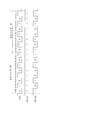
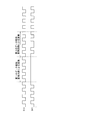
- FIG. 6 is a signal waveform diagram for describing processing performed in the first data array conversion circuit and the second data array conversion circuit in the embodiment. In the said embodiment, it is a signal waveform diagram for demonstrating conversion of a data array. It is a signal waveform diagram for demonstrating the effect in the said embodiment. It is a figure for demonstrating addition of an identification signal in the 1st modification of the said embodiment.
- FIG. 6 is a signal waveform diagram for describing processing performed in the first data array conversion circuit and the second data array conversion circuit in the embodiment. In the said embodiment, it is a signal waveform diagram for demonstrating conversion of a data array. It is a signal waveform diagram for demonstrating the effect in the said embodiment.
- FIG. 11 is a block diagram illustrating a configuration of a main part related to transmission of a digital video signal from a liquid crystal controller to a source driver in a first modification of the embodiment. It is a block diagram for demonstrating the 2nd modification of the said embodiment. It is a block diagram which shows the structure of the liquid crystal controller in the 3rd modification of the said embodiment.
- FIG. 11 is a block diagram for explaining transmission of image data inside a liquid crystal display device in a conventional example. It is a signal waveform diagram for demonstrating the subject in a prior art example.
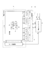
- FIG. 2 is a block diagram showing the overall configuration of the liquid crystal display device according to one embodiment of the present invention.
- the liquid crystal display device includes a liquid crystal controller (control circuit) 10, a source driving unit 20 including a plurality of source drivers (video signal line driving circuit) 200 in the form of an IC chip, and a gate driving unit. 30 and a display unit 40.
- the gate driving unit 30 and the display unit 40 are included in the liquid crystal panel 5. That is, the gate driving unit 30 is monolithically formed on the glass substrate in the liquid crystal panel 5.
- An input terminal of the source driver 200 is connected to a terminal on the source substrate 6 realized by a PCB (Printed Circuit Board) or the like, and an output terminal of the source driver 200 is connected to a terminal in the liquid crystal panel 5.
- the source driver 20 and the gate driver 30 may be realized by a method other than the above.
- the display unit 40 has a plurality of source bus lines (video signal lines) SL, a plurality of gate bus lines (scanning signal lines) GL, and intersections between the source bus lines and the gate bus lines. And a plurality of pixel forming portions provided. The plurality of pixel forming portions are arranged in a matrix to form a pixel array.
- Each pixel forming portion includes a TFT 46 which is a switching element having a gate terminal connected to a gate bus line GL passing through a corresponding intersection and a source terminal connected to a source bus line SL passing through the intersection, A liquid crystal capacitor 42 formed by the pixel electrode 41 connected to the drain terminal, the common electrode 44 and the auxiliary capacitance electrode 45 provided in common to the plurality of pixel formation portions, and the pixel electrode 41 and the common electrode 44. And an auxiliary capacitance 43 formed by the pixel electrode 41 and the auxiliary capacitance electrode 45.
- the liquid crystal capacitor 42 and the auxiliary capacitor 43 constitute a pixel capacitor. In the display unit 40 of FIG. 2, only the components corresponding to one pixel formation unit are shown.
- the liquid crystal controller 10 receives an input image signal Din, which is image data, and a timing signal TG such as a horizontal synchronization signal and a vertical synchronization signal, and receives a digital video signal DV1 and a plurality of signals (for controlling the operation of the source driver 20).
- a source control signal SS which is a source start pulse signal, a source clock signal, a latch strobe signal, etc.
- a gate which is a plurality of signals (gate start pulse signal, gate clock signal, etc.) for controlling the operation of the gate driver 30
- a control signal SG is output.
- the source driver 200 in the source driver 20 receives the digital video signal DV1 and the source control signal SS output from the liquid crystal controller 10, and applies a driving video signal to each source bus line. Based on the gate control signal SG output from the liquid crystal controller 10, the gate driver 30 repeats application of the active scanning signal to each gate bus line with one vertical scanning period as a cycle.
- an image based on the input image signal Din is displayed on the display unit 40 by applying the drive video signal to each source bus line and applying the scanning signal to each gate bus line.
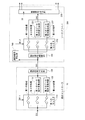
- FIG. 1 is a block diagram showing a configuration of a main part related to transmission of the digital video signal DV1 from the liquid crystal controller 10 to the source driver 200.
- the liquid crystal controller 10 includes a selector 110, a first data array conversion circuit 121, and a second data array conversion circuit 122.
- the source driver 200 includes a selector 210, a first data array restoration circuit 221, and a second data array restoration circuit 222.
- the selector 110 in the liquid crystal controller 10 is referred to as a “first selector”
- the selector 210 in the source driver 200 is referred to as a “second selector”.
- the first selector 110 switches the process for the input image signal Din between the following three processes.
- the data array is not converted for the input image signal Din, and the input image signal Din is transmitted to the source driver 200 as the digital video signal DV1 in the data array as it is.
- the input image signal Din is supplied to the first data array conversion circuit 121.
- the first data array conversion circuit 121 inverts even-bit values for each unit data (8-bit data) included in the input image signal Din.
- the input image signal Din thus subjected to the data array conversion is transmitted to the source driver 200 as the digital video signal DV1.
- the input image signal Din is supplied to the second data array conversion circuit 122.
- the second data array conversion circuit 122 inverts the value of the upper 4 bits for each unit data (8-bit data) included in the input image signal Din. That is, when focusing on the value of the upper 4 bits of the unit data, if the value is 0, the value is converted to 1, and if the value is 1, the value is converted to 0.
- the input image signal Din thus converted in data arrangement is transmitted to the source driver 200 as the digital video signal DV1.
- the liquid crystal controller 10 when an input image signal having a waveform indicated by Din in FIG. 3 is given to the liquid crystal controller 10, when the data array conversion is performed by the first data array conversion circuit 121, the reference numeral DV1 (a) in FIG. Is transmitted to the source driver 200, and the data array conversion is performed by the second data array conversion circuit 122, the digital video signal having the waveform indicated by reference numeral DV1 (b) in FIG. It is transmitted to the driver 200.
- the first data array conversion circuit 121 inverts the even bit value of each unit data
- the second data array conversion circuit 122 inverts the upper 4 bit value of each unit data.
- An inversion rule that specifies one or less than 8 bits that invert the value among the 8 bits constituting the unit data is defined, and data array conversion processing (processing that inverts the bit value) according to the inversion rule If a configuration including a circuit (data array conversion circuit) is provided, the value of any bit in the unit data may be inverted.
- the first selector 110 selects the above three processes while sequentially switching them every predetermined period based on the control signal SEL1. For example, when the first process, the second process, and the third process are sequentially switched for each unit data (8-bit data), the input image signal having the waveform indicated by the symbol Din in FIG. 4, a digital video signal having a waveform indicated by reference numeral DV 1 in FIG. 4 is transmitted from the liquid crystal controller 10 to the source driver 200.
- the control signal SEL1 to be supplied to the first selector 110 may be generated based on, for example, a timing signal TG sent from the outside so that the three processes are sequentially switched every predetermined period.
- the second selector 210 switches the process for the digital video signal DV1 sent from the liquid crystal controller 10 between the following three processes.
- the digital video signal DV1 is not subjected to data array conversion, and the digital video signal DV1 is converted to the video signal output unit 230 as the digital video signal DV2 with the data array unchanged.
- the digital video signal DV1 is supplied to the first data array restoration circuit 221.
- the first data array restoration circuit 221 performs a process of inverting the value of even bits for each unit data in the same manner as the first data array conversion circuit 121, and provides digital video to be supplied to the video signal output unit 230.
- the signal DV2 is output. Therefore, when the digital video signal DV1 after the data array conversion by the first data array conversion circuit 121 is given to the first data array recovery circuit 221, the digital video signal output from the first data array recovery circuit 221 The data array of DV2 is the same as the data array of the input image signal Din. When the third process is selected, the digital video signal DV1 is supplied to the second data array restoration circuit 222.
- the second data array restoration circuit 222 performs a process of inverting the value of the upper 4 bits for each unit data, and outputs the digital data to the video signal output unit 230.
- the video signal DV2 is output. Accordingly, when the digital video signal DV1 after the data array conversion by the second data array conversion circuit 122 is given to the second data array recovery circuit 222, the digital video signal output from the second data array recovery circuit 222 The data array of DV2 is the same as the data array of the input image signal Din.
- the video signal output unit 230 receives the digital video signal DV2 and the source control signal SS, and applies a driving video signal to each source bus line.
- the second selector 210 selects the above three processes while sequentially switching them every predetermined period based on the control signal SEL2.
- the data array conversion must be performed again by the first data array restoration circuit 221.
- the unit data that has undergone the data array conversion by the second data array conversion circuit 122 must be subjected to the data array conversion again by the second data array restoration circuit 222.
- the liquid crystal controller 10 generates a synchronization signal so that the conversion of the data arrangement for each unit data is performed in the same manner by the liquid crystal controller 10 and the source driver 200, and the source driver 200 uses the synchronization signal as the control signal SEL2.
- the data array conversion step is realized by the data array conversion processing by the first data array conversion circuit 121 and the second data array conversion circuit 122, and the digital conversion from the liquid crystal controller 10 to the source driver 200 is performed.
- the data transmission step is realized by the transmission of the video signal DV1
- the data arrangement restoration step is realized by the data arrangement conversion processing by the first data arrangement restoration circuit 221 and the second data arrangement restoration circuit 222.
- the liquid crystal controller 10 when image data is transmitted from the liquid crystal controller 10 to the source driver 200 in the liquid crystal display device, the liquid crystal controller 10 performs “no conversion” and “first data array conversion circuit” on the image data. Three processes of “data array conversion by 121 (inversion of even-bit value)” and “data array conversion by second data array conversion circuit 122 (inversion of upper 4 bits value)” are performed for each unit data. It is done sequentially. Therefore, when an input image signal having a waveform indicated by Din in FIG. 5 is given to the liquid crystal controller 10 as image data, the waveform of the digital video signal transmitted from the liquid crystal controller 91 to the source driver 92 is indicated by DV1 in FIG. It becomes a waveform shown by.
- a current peak occurs as indicated by reference numeral I in FIG. From FIG. 5 and FIG. 11 (conventional example), it is understood that the frequency of occurrence of current peaks is reduced in this embodiment compared to the conventional example.
- image data whose data value regularly changes at a constant short period is supplied from the liquid crystal controller 10 while suppressing an increase in power consumption. Transmission to the driver 200 is possible.
- the configuration is such that the synchronization signal is supplied from the liquid crystal controller 10 to the source driver 200 so that the conversion of the data arrangement for each unit data is performed in the same way by the liquid crystal controller 10 and the source driver 200.
- this invention is not limited to this, For example, it can also be set as the following structures.
- an identification signal for identifying the processing performed by the liquid crystal controller 10 is added to the digital video signal DV1 transmitted from the liquid crystal controller 10 to the source driver 200.
- a 2-bit identification signal is added for each unit data constituting the image data.
- FIG. 7 is a block diagram showing a configuration of a main part related to transmission of a digital video signal from the liquid crystal controller 10 to the source driver 200 in the present modification.
- the liquid crystal controller 10 is provided with an identification signal adding unit (bit adding unit) 130
- the source driver 200 has an identification signal determining unit (bit value determining unit).
- 240 and an identification signal deletion unit 241 are provided.
- the identification signal adding unit 130 adds a 2-bit identification signal having a value corresponding to the processing content in the liquid crystal controller 10 for each unit data to the digital video signal DV1. Note that a bit addition step is realized by this processing.
- the digital video signal DV1 to which the identification signal is added is transmitted from the liquid crystal controller 10 to the source driver 200, and is given to the identification signal determination unit 240 and the identification signal deletion unit 241.
- the identification signal determination unit 240 determines processing performed by the liquid crystal controller 10 for each unit data based on the identification signal added to the digital video signal DV1.
- the identification signal deletion unit 241 deletes the identification signal from the digital video signal DV1.
- the second selector 210 selects processing to be applied to the digital video signal DV1 based on the determination result in the identification signal determination unit 240. By the operation as described above, the conversion of the data arrangement for each unit data is reliably performed in the same manner in the liquid crystal controller 10 and the source driver 200.
- the process of converting the data array is performed on the input image signal Din regardless of the content of the input image signal Din.
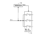
- the liquid crystal controller 10 is configured to include an image determination unit 140 as a data determination unit for determining whether the input image signal Din is a moving image or a still image (see FIG. 8), and the input image signal Din is a still image. Data array conversion may be performed only in the case of an image.
- both the liquid crystal controller 10 and the source driver 200 perform the first processing (processing that outputs the input data as it is without inverting the bit value of each unit data. ) Is selected. As a result, the burden on the liquid crystal controller 10 and the source driver 200 can be reduced.
- the data determination step is realized by processing in the image determination unit 140.
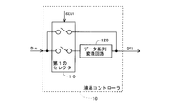
- the liquid crystal controller 10 may have only one data arrangement conversion circuit 120, or the liquid crystal controller 10 may have three or more data arrangement conversion circuits.
- a data array restoration circuit must be provided so as to correspond one-to-one with the data array conversion circuit in the liquid crystal controller 10, and the corresponding data array conversion circuit and data array restoration circuit are provided. In the same way, the bit value must be inverted for the unit data.
- the liquid crystal display device has been described as an example, but the present invention is not limited to this.
- the present invention can also be applied to other display devices such as an organic EL (Electro Luminescence).
- the data transmission method according to the present invention is not limited to data transmission within the display device, but can also be applied to data transmission between two devices that transmit and receive serial data.
- the data to be transmitted / received may be data externally given to the transmission-side device or data generated inside the transmission-side device.
- DESCRIPTION OF SYMBOLS 10 Liquid crystal controller 110 ... 1st selector 120 ... Data arrangement conversion circuit 121 ... 1st data arrangement conversion circuit 122 ... 2nd data arrangement conversion circuit 130 ... Identification signal addition part 140 ... Image determination part 20 ... Source drive part DESCRIPTION OF SYMBOLS 200 ... Source driver 210 ... 2nd selector 221 ... 1st data arrangement restoration circuit 222 ... 2nd data arrangement restoration circuit 230 ... Video signal output part 240 ... Identification signal determination part 241 ... Identification signal deletion part Din ... Input image Signal DV1 ... Digital video signal
Landscapes
- Engineering & Computer Science (AREA)
- Physics & Mathematics (AREA)
- Computer Hardware Design (AREA)
- General Physics & Mathematics (AREA)
- Theoretical Computer Science (AREA)
- Chemical & Material Sciences (AREA)
- Crystallography & Structural Chemistry (AREA)
- Control Of Indicators Other Than Cathode Ray Tubes (AREA)
Abstract
一定の短い周期でデータ値が変化するようなデータについてのシリアル伝送を消費電力の増大を抑制しつつ行うことのできる方法を提供する。 液晶コントローラ(10)では、第1のデータ配列変換回路(121)や第2のデータ配列変換回路(122)によって、入力画像信号(Din)に含まれるデータに対して、所定期間毎にデータ配列の変換が施される。データ配列の変換は、各データの予め定められたビットの値を反転させることによって行われる。データ配列の変換後のデータは、デジタル映像信号(DV1)としてソースドライバ(200)に伝送される。ソースドライバ(200)では、第1のデータ配列復元回路(221)や第2のデータ配列復元回路(222)によって、デジタル映像信号(DV1)に含まれる各データに対して、液晶コントローラ(10)で行われたのと同様のデータ配列の変換が行われる。
Description
本発明は、データ伝送方法に関し、特に、表示装置内における画像信号の伝送方法に関する。
一般的な液晶表示装置には、液晶パネルを駆動するための1または複数のドライバ(以下、「液晶ドライバ」という。)と、外部から送られる画像信号(以下、「入力画像信号」という。)や同期信号に基づいて液晶ドライバの動作を制御するための液晶コントローラとが設けられている。液晶ドライバとしては、典型的には、液晶パネル内のゲートバスライン(走査信号線)を駆動するためのゲートドライバ(走査信号線駆動回路)と液晶パネル内のソースバスライン(映像信号線)を駆動するためのソースドライバ(映像信号線駆動回路)とが液晶表示装置に設けられている。
図10は、液晶表示装置の内部における画像データの伝送について説明するためのブロック図である。液晶コントローラ91には、画像データである入力画像信号Dinが外部から与えられる。そして、液晶コントローラ91でタイミングの調整などが行われ、入力画像信号Dinに基づいて生成されるデジタル形式の信号(以下、「デジタル映像信号」という。)DVが液晶コントローラ91からソースドライバ92に伝送される。液晶コントローラ91からソースドライバ92へのデジタル映像信号DVの伝送方法については、典型的には、1本の信号線を用いて1ビットずつデータを伝送するシリアル伝送が採用されている。ソースドライバ92は、液晶コントローラ91から送られるデジタル映像信号DVに基づいて、電圧信号である映像信号を各ソースバスラインに印加する。
ところで、液晶表示装置などの表示装置においては、従来より低消費電力化が課題となっている。そのため、データ伝送時の消費電力についても低減が図られている。例えば、日本の特開2009-267624号公報に開示された発明によると、シリアル伝送に関し、消費電力の低減を図るために、連続して同じ振幅値を取らず、かつ、一周期毎に振幅値の極性が反転するように、データの伝送が行われている。
シリアル伝送においては、上述したように1ビットずつデータが伝送されるところ、データの伝送中にビットの値の反転が多く行われるほど消費電力が増大する。何故ならば、ビットの値の変化に応じて回路内で電流が生じるからである。このため、静止画像のデータなど一定の短い周期で規則的にデータ値が変化するようなデータの伝送が表示装置内で行われると、消費電力は大きくなる。例えば、図10に示した構成において、図11で符号Dinで示す波形の入力画像信号が液晶コントローラ91に与えられると、図11で符号DVで示す波形のデジタル映像信号が液晶コントローラ91からソースドライバ92に伝送される。このとき、図11で符号Iで示すように一定の短い周期で電流のピークが生じ、その結果、消費電力が大きくなる。上記日本の特開2009-267624号公報に開示された発明によっても、データ値の反転が行われるだけで、伝送される信号の周波数は変化しないので、一定の短い周期で規則的にデータ値が変化するようなデータの伝送が行われる場合には、消費電力低減の効果は大きくは得られない。
そこで本発明は、一定の短い周期でデータ値が変化するようなデータについてのシリアル伝送を消費電力の増大を抑制しつつ行うことのできる方法を提供することを目的とする。
本発明の第1の局面は、nビット(nは2以上の整数)からなる単位データを含むデータを送信部から受信部にシリアル伝送するデータ伝送方法であって、
前記送信部に与えられたデータもしくは前記送信部で生成されたデータである伝送対象データに関し、前記単位データを構成するnビットのうち値を反転させるビットを特定する予め定められた反転規則に基づいて、前記単位データごとに1個以上n個未満のビットの値を反転させる第1の反転処理を行うデータ配列変換ステップと、
前記データ配列変換ステップで得られたデータを前記送信部から前記受信部に伝送するデータ伝送ステップと、
前記データ伝送ステップで前記受信部に伝送されたデータに関し、前記単位データごとに前記第1の反転処理で値の反転が行われたビットの値を反転させる第2の反転処理を行うデータ配列復元ステップと
を含むことを特徴とする。
前記送信部に与えられたデータもしくは前記送信部で生成されたデータである伝送対象データに関し、前記単位データを構成するnビットのうち値を反転させるビットを特定する予め定められた反転規則に基づいて、前記単位データごとに1個以上n個未満のビットの値を反転させる第1の反転処理を行うデータ配列変換ステップと、
前記データ配列変換ステップで得られたデータを前記送信部から前記受信部に伝送するデータ伝送ステップと、
前記データ伝送ステップで前記受信部に伝送されたデータに関し、前記単位データごとに前記第1の反転処理で値の反転が行われたビットの値を反転させる第2の反転処理を行うデータ配列復元ステップと
を含むことを特徴とする。
本発明の第2の局面は、本発明の第1の局面において、
前記単位データごとに前記第1の反転処理で用いられた反転規則に応じた値の識別用ビットを付加するビット付加ステップを更に含み、
前記データ配列復元ステップでは、前記単位データに付加されている前記識別用ビットの値に応じた反転規則に基づいて、前記第2の反転処理が行われることを特徴とする。
前記単位データごとに前記第1の反転処理で用いられた反転規則に応じた値の識別用ビットを付加するビット付加ステップを更に含み、
前記データ配列復元ステップでは、前記単位データに付加されている前記識別用ビットの値に応じた反転規則に基づいて、前記第2の反転処理が行われることを特徴とする。
本発明の第3の局面は、本発明の第1の局面において、
前記反転規則は予め複数定められ、
前記データ配列変換ステップでは、複数の前記反転規則を所定期間ずつ順次に用いることによって前記第1の反転処理が行われることを特徴とする。
前記反転規則は予め複数定められ、
前記データ配列変換ステップでは、複数の前記反転規則を所定期間ずつ順次に用いることによって前記第1の反転処理が行われることを特徴とする。
本発明の第4の局面は、本発明の第1の局面において、
前記伝送対象データの内容を判別するデータ判別ステップを更に含み、
前記データ判別ステップで得られた結果に応じて、前記データ配列変換ステップにおける前記第1の反転処理および前記データ配列復元ステップにおける前記第2の反転処理の実行の有無が切り替えられることを特徴とする。
前記伝送対象データの内容を判別するデータ判別ステップを更に含み、
前記データ判別ステップで得られた結果に応じて、前記データ配列変換ステップにおける前記第1の反転処理および前記データ配列復元ステップにおける前記第2の反転処理の実行の有無が切り替えられることを特徴とする。
本発明の第5の局面は、映像信号を伝達するための複数の映像信号線を駆動する映像信号線駆動回路と、nビット(nは2以上の整数)からなる単位データを含む画像データを前記映像信号線駆動回路にシリアル伝送する制御回路とを備えた表示装置であって、
前記制御回路は、前記画像データに関し前記単位データを構成するnビットのうち値を反転させるビットを特定する予め定められた反転規則に基づいて前記単位データごとに1個以上n個未満のビットの値を反転させる第1の反転処理を行うデータ配列変換回路を含み、
前記映像信号線駆動回路は、前記制御回路から伝送された画像データに関し前記単位データごとに前記第1の反転処理で値の反転が行われたビットの値を反転させる第2の反転処理を行うデータ配列復元回路を含むことを特徴とする。
前記制御回路は、前記画像データに関し前記単位データを構成するnビットのうち値を反転させるビットを特定する予め定められた反転規則に基づいて前記単位データごとに1個以上n個未満のビットの値を反転させる第1の反転処理を行うデータ配列変換回路を含み、
前記映像信号線駆動回路は、前記制御回路から伝送された画像データに関し前記単位データごとに前記第1の反転処理で値の反転が行われたビットの値を反転させる第2の反転処理を行うデータ配列復元回路を含むことを特徴とする。
本発明の第6の局面は、本発明の第5の局面において、
前記制御回路は、前記単位データごとに前記第1の反転処理で用いられた反転規則に応じた値の識別用ビットを付加するビット付加部を更に含み、
前記映像信号線駆動回路は、前記単位データに付加されている前記識別用ビットの値を判定するビット値判定部を更に含み、
前記映像信号線駆動回路では、前記ビット値判定部による判定結果に基づいて選択されるデータ配列復元回路によって前記第2の反転処理が行われることを特徴とする。
前記制御回路は、前記単位データごとに前記第1の反転処理で用いられた反転規則に応じた値の識別用ビットを付加するビット付加部を更に含み、
前記映像信号線駆動回路は、前記単位データに付加されている前記識別用ビットの値を判定するビット値判定部を更に含み、
前記映像信号線駆動回路では、前記ビット値判定部による判定結果に基づいて選択されるデータ配列復元回路によって前記第2の反転処理が行われることを特徴とする。
本発明の第7の局面は、本発明の第5の局面において、
前記制御回路には、互いに異なる反転規則に基づいて前記第1の反転処理を行う複数のデータ配列変換回路が含まれ、
前記映像信号線駆動回路には、前記複数のデータ配列変換回路に1対1で対応する複数のデータ配列復元回路が含まれ、
前記制御回路では、前記複数のデータ配列変換回路が所定期間ずつ順次に選択されて前記第1の反転処理が行われ、
前記映像信号線駆動回路では、各単位データについて前記第2の反転処理が行われる際、前記制御回路で選択されたデータ配列変換回路に対応するデータ配列復元回路が選択されることを特徴とする。
前記制御回路には、互いに異なる反転規則に基づいて前記第1の反転処理を行う複数のデータ配列変換回路が含まれ、
前記映像信号線駆動回路には、前記複数のデータ配列変換回路に1対1で対応する複数のデータ配列復元回路が含まれ、
前記制御回路では、前記複数のデータ配列変換回路が所定期間ずつ順次に選択されて前記第1の反転処理が行われ、
前記映像信号線駆動回路では、各単位データについて前記第2の反転処理が行われる際、前記制御回路で選択されたデータ配列変換回路に対応するデータ配列復元回路が選択されることを特徴とする。
本発明の第8の局面は、本発明の第5の局面において、
前記制御回路は、前記画像データの内容を判別するデータ判別部を更に含み、
前記データ判別部によって得られた結果に応じて、前記データ配列変換回路による前記第1の反転処理および前記データ配列復元回路による前記第2の反転処理の実行の有無が切り替えられることを特徴とする。
前記制御回路は、前記画像データの内容を判別するデータ判別部を更に含み、
前記データ判別部によって得られた結果に応じて、前記データ配列変換回路による前記第1の反転処理および前記データ配列復元回路による前記第2の反転処理の実行の有無が切り替えられることを特徴とする。
本発明の第1の局面によれば、データのシリアル伝送が行われる際に、送信部において、伝送対象データを構成する単位データ毎に、予め定められたビットの値を反転させる処理が行われる。このため、伝送対象データが一定の短い周期で規則的にデータ値が変化するようなデータであるときに、当該伝送対象データをデータ値の変化が少ないデータに変換し、その変換後のデータを送信部から受信部に伝送することが可能となる。これにより、データのシリアル伝送に際して、電流ピークの発生頻度が低減され、消費電力の増大が抑制される。
本発明の第2の局面によれば、送信部での処理内容を特定するための値を持つ識別用ビットが伝送対象データに付加され、受信部では当該識別用ビットの値に基づいて処理が行われる。これにより、送信部で変換が施されたデータを確実に受信部で復元することが可能となる。
本発明の第3の局面によれば、データ伝送に起因する電流ピークの発生を効果的に分散させることが可能となる。
本発明の第4の局面によれば、ビットの値を反転させる処理の実行の有無を伝送対象データの内容に応じて切り替えることが可能となる。これにより、送信部および受信部の負担が軽減される。
本発明の第5の局面によれば、表示装置内における制御回路から映像信号線駆動回路への画像データの伝送に際し、制御回路において、画像データを構成する単位データ毎に、予め定められたビットの値を反転させる処理が行われる。このため、伝送されるべき画像データが一定の短い周期で規則的にデータ値が変化するようなデータであるときに、当該画像データをデータ値の変化が少ないデータに変換し、その変換後のデータを制御回路から映像信号線駆動回路に伝送することが可能となる。これにより、画像データの伝送に起因する電流ピークの発生頻度が低減され、消費電力の増大が抑制される。
本発明の第6の局面によれば、表示装置において、制御回路での処理内容を特定するための値を持つ識別用ビットが画像データに付加され、映像信号線駆動回路では当該識別用ビットの値に基づいて処理が行われる。これにより、制御回路で変換が施された画像データを確実に映像信号線駆動回路で復元することが可能となる。
本発明の第7の局面によれば、表示装置の制御回路-映像信号線駆動回路間での画像データの伝送に起因する電流ピークの発生を効果的に分散させることが可能となる。
本発明の第8の局面によれば、ビットの値を反転させる処理の実行の有無を画像データの内容に応じて切り替えることが可能となる。これにより、制御回路および映像信号線駆動回路の負担が軽減される。
<1.全体構成および動作>
図2は、本発明の一実施形態に係る液晶表示装置の全体構成を示すブロック図である。図2に示すように、この液晶表示装置は、液晶コントローラ(制御回路)10と、ICチップの形態の複数のソースドライバ(映像信号線駆動回路)200からなるソース駆動部20と、ゲート駆動部30と、表示部40とを備えている。ゲート駆動部30と表示部40とは液晶パネル5内に含まれている。すなわち、ゲート駆動部30については、液晶パネル5内においてガラス基板上にモノリシックに形成されている。ソースドライバ200の入力端子は、PCB(Printed Circuit Board)などで実現されるソース基板6上の端子に接続され、ソースドライバ200の出力端子は、液晶パネル5内の端子に接続されている。なお、ソース駆動部20およびゲート駆動部30については、上記以外の方式で実現されていても良い。
図2は、本発明の一実施形態に係る液晶表示装置の全体構成を示すブロック図である。図2に示すように、この液晶表示装置は、液晶コントローラ(制御回路)10と、ICチップの形態の複数のソースドライバ(映像信号線駆動回路)200からなるソース駆動部20と、ゲート駆動部30と、表示部40とを備えている。ゲート駆動部30と表示部40とは液晶パネル5内に含まれている。すなわち、ゲート駆動部30については、液晶パネル5内においてガラス基板上にモノリシックに形成されている。ソースドライバ200の入力端子は、PCB(Printed Circuit Board)などで実現されるソース基板6上の端子に接続され、ソースドライバ200の出力端子は、液晶パネル5内の端子に接続されている。なお、ソース駆動部20およびゲート駆動部30については、上記以外の方式で実現されていても良い。
表示部40には、複数本のソースバスライン(映像信号線)SLと、複数本のゲートバスライン(走査信号線)GLと、それらソースバスラインとゲートバスラインとの交差点にそれぞれ対応して設けられた複数個の画素形成部とが含まれている。上記複数個の画素形成部はマトリクス状に配置されて画素アレイを構成している。各画素形成部は、対応する交差点を通過するゲートバスラインGLにゲート端子が接続されると共に当該交差点を通過するソースバスラインSLにソース端子が接続されたスイッチング素子であるTFT46と、そのTFT46のドレイン端子に接続された画素電極41と、上記複数個の画素形成部に共通的に設けられた共通電極44および補助容量電極45と、画素電極41と共通電極44とによって形成される液晶容量42と、画素電極41と補助容量電極45とによって形成される補助容量43とが含まれている。液晶容量42と補助容量43とによって画素容量が構成されている。なお、図2の表示部40内には、1つの画素形成部に対応する構成要素のみを示している。
液晶コントローラ10は、画像データである入力画像信号Dinおよび水平同期信号や垂直同期信号などのタイミング信号TGを受け取り、デジタル映像信号DV1と、ソース駆動部20の動作を制御するための複数の信号(ソーススタートパルス信号,ソースクロック信号,ラッチストローブ信号など)であるソース制御信号SSと、ゲート駆動部30の動作を制御するための複数の信号(ゲートスタートパルス信号,ゲートクロック信号など)であるゲート制御信号SGとを出力する。ソース駆動部20内のソースドライバ200は、液晶コントローラ10から出力されるデジタル映像信号DV1とソース制御信号SSとを受け取り、各ソースバスラインに駆動用映像信号を印加する。ゲート駆動部30は、液晶コントローラ10から出力されるゲート制御信号SGに基づいて、アクティブな走査信号の各ゲートバスラインへの印加を1垂直走査期間を周期として繰り返す。
以上のようにして、各ソースバスラインに駆動用映像信号が印加され、各ゲートバスラインに走査信号が印加されることにより、入力画像信号Dinに基づく画像が表示部40に表示される。
<2.データ伝送方法>
次に、液晶コントローラ10からソースドライバ200への画像データの伝送方法について説明する。この画像データの伝送に関しては、シリアル伝送が行われ、液晶コントローラ10が送信部として機能し、ソースドライバ200が受信部として機能する。本実施形態においては、画像データは、まず、入力画像信号Dinとして液晶コントローラ10に与えられ、その後、デジタル映像信号DV1として液晶コントローラ10からソースドライバ200に伝送される。なお、以下の説明においては、入力画像信号Dinに含まれる各データは8ビットで構成されているものと仮定する。以下、このように8ビットで構成された1つのまとまりのあるデータのことを「単位データ」ともいう。また、以下の説明における「データ配列」とは、単位データ(ここでは8ビットのデータ)を構成する複数のビットの値(0または1)の並び方のことをいう。
次に、液晶コントローラ10からソースドライバ200への画像データの伝送方法について説明する。この画像データの伝送に関しては、シリアル伝送が行われ、液晶コントローラ10が送信部として機能し、ソースドライバ200が受信部として機能する。本実施形態においては、画像データは、まず、入力画像信号Dinとして液晶コントローラ10に与えられ、その後、デジタル映像信号DV1として液晶コントローラ10からソースドライバ200に伝送される。なお、以下の説明においては、入力画像信号Dinに含まれる各データは8ビットで構成されているものと仮定する。以下、このように8ビットで構成された1つのまとまりのあるデータのことを「単位データ」ともいう。また、以下の説明における「データ配列」とは、単位データ(ここでは8ビットのデータ)を構成する複数のビットの値(0または1)の並び方のことをいう。
図1は、液晶コントローラ10からソースドライバ200へのデジタル映像信号DV1の伝送に関係する要部の構成を示すブロック図である。液晶コントローラ10は、セレクタ110と第1のデータ配列変換回路121と第2のデータ配列変換回路122とを有している。ソースドライバ200は、セレクタ210と第1のデータ配列復元回路221と第2のデータ配列復元回路222とを有している。なお、以下の説明においては、液晶コントローラ10内のセレクタ110のことを「第1のセレクタ」といい、ソースドライバ200内のセレクタ210のことを「第2のセレクタ」という。
<2.1 液晶コントローラ内の動作>
まず、液晶コントローラ10内の各構成要素の動作について説明する。第1のセレクタ110は、入力画像信号Dinに対する処理を次の3つの処理の間で切り替える。第1の処理が選択されると、入力画像信号Dinに対してデータ配列の変換が施されることはなく、入力画像信号Dinがそのままのデータ配列でデジタル映像信号DV1としてソースドライバ200に伝送される。第2の処理が選択されると、入力画像信号Dinが第1のデータ配列変換回路121に与えられる。第1のデータ配列変換回路121は、入力画像信号Dinに含まれる各単位データ(8ビットのデータ)に対して、偶数ビットの値を反転させる。すなわち、単位データの偶数ビットの値に着目したとき、値が0であれば当該値は1に変換され、値が1であれば当該値は0に変換される。第2の処理では、このように入力画像信号Dinに対してデータ配列の変換が施されたものが、デジタル映像信号DV1としてソースドライバ200に伝送される。第3の処理が選択されると、入力画像信号Dinが第2のデータ配列変換回路122に与えられる。第2のデータ配列変換回路122は、入力画像信号Dinに含まれる各単位データ(8ビットのデータ)に対して、上位4ビットの値を反転させる。すなわち、単位データの上位4ビットの値に着目したとき、値が0であれば当該値は1に変換され、値が1であれば当該値は0に変換される。第3の処理では、このように入力画像信号Dinに対してデータ配列の変換が施されたものが、デジタル映像信号DV1としてソースドライバ200に伝送される。
まず、液晶コントローラ10内の各構成要素の動作について説明する。第1のセレクタ110は、入力画像信号Dinに対する処理を次の3つの処理の間で切り替える。第1の処理が選択されると、入力画像信号Dinに対してデータ配列の変換が施されることはなく、入力画像信号Dinがそのままのデータ配列でデジタル映像信号DV1としてソースドライバ200に伝送される。第2の処理が選択されると、入力画像信号Dinが第1のデータ配列変換回路121に与えられる。第1のデータ配列変換回路121は、入力画像信号Dinに含まれる各単位データ(8ビットのデータ)に対して、偶数ビットの値を反転させる。すなわち、単位データの偶数ビットの値に着目したとき、値が0であれば当該値は1に変換され、値が1であれば当該値は0に変換される。第2の処理では、このように入力画像信号Dinに対してデータ配列の変換が施されたものが、デジタル映像信号DV1としてソースドライバ200に伝送される。第3の処理が選択されると、入力画像信号Dinが第2のデータ配列変換回路122に与えられる。第2のデータ配列変換回路122は、入力画像信号Dinに含まれる各単位データ(8ビットのデータ)に対して、上位4ビットの値を反転させる。すなわち、単位データの上位4ビットの値に着目したとき、値が0であれば当該値は1に変換され、値が1であれば当該値は0に変換される。第3の処理では、このように入力画像信号Dinに対してデータ配列の変換が施されたものが、デジタル映像信号DV1としてソースドライバ200に伝送される。
例えば、図3で符号Dinで示す波形の入力画像信号が液晶コントローラ10に与えられた場合、第1のデータ配列変換回路121でデータ配列の変換が行われると、図3で符号DV1(a)で示す波形のデジタル映像信号がソースドライバ200に伝送され、第2のデータ配列変換回路122でデータ配列の変換が行われると、図3で符号DV1(b)で示す波形のデジタル映像信号がソースドライバ200に伝送される。
なお、本実施形態においては、第1のデータ配列変換回路121では各単位データの偶数ビットの値が反転し、第2のデータ配列変換回路122では各単位データの上位4ビットの値が反転する。しかしながら、本発明はこれに限定されない。単位データを構成する8ビットのうち値を反転させる1個以上8個未満のビットを特定する反転規則を定め、当該反転規則に従ったデータ配列の変換処理(ビットの値を反転させる処理)を行う回路(データ配列変換回路)を備える構成にすれば、単位データ内のいずれのビットの値が反転するようにしても良い。
ところで、第1のセレクタ110は、制御信号SEL1に基づいて、上記3つの処理を所定期間毎に順次に切り替えつつ選択する。例えば、第1の処理と第2の処理と第3の処理とを単位データ(8ビットのデータ)ごとに順次に切り替えた場合、図4で符号Dinで示す波形の入力画像信号が液晶コントローラ10に与えられると、図4で符号DV1で示す波形のデジタル映像信号が液晶コントローラ10からソースドライバ200に伝送される。なお、第1のセレクタ110に与える制御信号SEL1については、上記3つの処理が所定期間毎に順次に切り替えられるよう、例えば外部から送られるタイミング信号TGに基づいて生成すれば良い。
<2.2 ソースドライバ内の動作>
次に、ソースドライバ200内の各構成要素の動作について説明する。第2のセレクタ210は、液晶コントローラ10から送られるデジタル映像信号DV1に対する処理を次の3つの処理の間で切り替える。第1の処理が選択されると、デジタル映像信号DV1に対してデータ配列の変換が施されることはなく、デジタル映像信号DV1がそのままのデータ配列でデジタル映像信号DV2として映像信号出力部230に与えられる。第2の処理が選択されると、デジタル映像信号DV1が第1のデータ配列復元回路221に与えられる。第1のデータ配列復元回路221は、第1のデータ配列変換回路121と同じように各単位データに対して偶数ビットの値を反転させる処理を行い、映像信号出力部230に与えるためのデジタル映像信号DV2を出力する。従って、第1のデータ配列変換回路121によるデータ配列の変換後のデジタル映像信号DV1が第1のデータ配列復元回路221に与えられると、第1のデータ配列復元回路221から出力されるデジタル映像信号DV2のデータ配列は、入力画像信号Dinのデータ配列と同じになる。第3の処理が選択されると、デジタル映像信号DV1が第2のデータ配列復元回路222に与えられる。第2のデータ配列復元回路222は、第2のデータ配列変換回路122と同じように各単位データに対して上位4ビットの値を反転させる処理を行い、映像信号出力部230に与えるためのデジタル映像信号DV2を出力する。従って、第2のデータ配列変換回路122によるデータ配列の変換後のデジタル映像信号DV1が第2のデータ配列復元回路222に与えられると、第2のデータ配列復元回路222から出力されるデジタル映像信号DV2のデータ配列は、入力画像信号Dinのデータ配列と同じになる。映像信号出力部230は、デジタル映像信号DV2とソース制御信号SSとを受け取り、各ソースバスラインに駆動用映像信号を印加する。
次に、ソースドライバ200内の各構成要素の動作について説明する。第2のセレクタ210は、液晶コントローラ10から送られるデジタル映像信号DV1に対する処理を次の3つの処理の間で切り替える。第1の処理が選択されると、デジタル映像信号DV1に対してデータ配列の変換が施されることはなく、デジタル映像信号DV1がそのままのデータ配列でデジタル映像信号DV2として映像信号出力部230に与えられる。第2の処理が選択されると、デジタル映像信号DV1が第1のデータ配列復元回路221に与えられる。第1のデータ配列復元回路221は、第1のデータ配列変換回路121と同じように各単位データに対して偶数ビットの値を反転させる処理を行い、映像信号出力部230に与えるためのデジタル映像信号DV2を出力する。従って、第1のデータ配列変換回路121によるデータ配列の変換後のデジタル映像信号DV1が第1のデータ配列復元回路221に与えられると、第1のデータ配列復元回路221から出力されるデジタル映像信号DV2のデータ配列は、入力画像信号Dinのデータ配列と同じになる。第3の処理が選択されると、デジタル映像信号DV1が第2のデータ配列復元回路222に与えられる。第2のデータ配列復元回路222は、第2のデータ配列変換回路122と同じように各単位データに対して上位4ビットの値を反転させる処理を行い、映像信号出力部230に与えるためのデジタル映像信号DV2を出力する。従って、第2のデータ配列変換回路122によるデータ配列の変換後のデジタル映像信号DV1が第2のデータ配列復元回路222に与えられると、第2のデータ配列復元回路222から出力されるデジタル映像信号DV2のデータ配列は、入力画像信号Dinのデータ配列と同じになる。映像信号出力部230は、デジタル映像信号DV2とソース制御信号SSとを受け取り、各ソースバスラインに駆動用映像信号を印加する。
ところで、第2のセレクタ210は、制御信号SEL2に基づいて、上記3つの処理を所定期間毎に順次に切り替えつつ選択する。この点に関し、第1のデータ配列変換回路121によってデータ配列の変換が施された単位データについては第1のデータ配列復元回路221によって再度データ配列の変換が施されなければならず、また、第2のデータ配列変換回路122によってデータ配列の変換が施された単位データについては第2のデータ配列復元回路222によって再度データ配列の変換が施されなければならない。そこで、各単位データについてのデータ配列の変換が液晶コントローラ10とソースドライバ200とで同じように行われるよう、液晶コントローラ10で同期信号を生成し、当該同期信号を上記制御信号SEL2としてソースドライバ200に与える構成とする。
なお、本実施形態においては、第1のデータ配列変換回路121および第2のデータ配列変換回路122によるデータ配列の変換処理によってデータ配列変換ステップが実現され、液晶コントローラ10からソースドライバ200へのデジタル映像信号DV1の伝送によってデータ伝送ステップが実現され、第1のデータ配列復元回路221および第2のデータ配列復元回路222によるデータ配列の変換処理によってデータ配列復元ステップが実現されている。
<3.効果>
本実施形態によれば、液晶表示装置内における液晶コントローラ10からソースドライバ200への画像データの伝送に際し、液晶コントローラ10において、画像データに対して「無変換」,「第1のデータ配列変換回路121によるデータ配列の変換(偶数ビットの値の反転)」,および「第2のデータ配列変換回路122によるデータ配列の変換(上位4ビットの値の反転)」の3つの処理が単位データ毎に順次に行われる。このため、画像データとして図5で符号Dinで示す波形の入力画像信号が液晶コントローラ10に与えられたとき、液晶コントローラ91からソースドライバ92に伝送されるデジタル映像信号の波形は図5で符号DV1で示す波形となる。このとき、図5で符号Iで示すように電流のピークが生じる。図5および図11(従来例)より、本実施形態では従来例と比較して電流のピークの発生頻度が低減されることが把握される。以上のように、本実施形態によれば、液晶表示装置において、一定の短い周期で規則的にデータ値が変化するような画像データを、消費電力の増大を抑制しつつ、液晶コントローラ10からソースドライバ200に伝送することが可能となる。
本実施形態によれば、液晶表示装置内における液晶コントローラ10からソースドライバ200への画像データの伝送に際し、液晶コントローラ10において、画像データに対して「無変換」,「第1のデータ配列変換回路121によるデータ配列の変換(偶数ビットの値の反転)」,および「第2のデータ配列変換回路122によるデータ配列の変換(上位4ビットの値の反転)」の3つの処理が単位データ毎に順次に行われる。このため、画像データとして図5で符号Dinで示す波形の入力画像信号が液晶コントローラ10に与えられたとき、液晶コントローラ91からソースドライバ92に伝送されるデジタル映像信号の波形は図5で符号DV1で示す波形となる。このとき、図5で符号Iで示すように電流のピークが生じる。図5および図11(従来例)より、本実施形態では従来例と比較して電流のピークの発生頻度が低減されることが把握される。以上のように、本実施形態によれば、液晶表示装置において、一定の短い周期で規則的にデータ値が変化するような画像データを、消費電力の増大を抑制しつつ、液晶コントローラ10からソースドライバ200に伝送することが可能となる。
<4.変形例>
以下、上記実施形態の変形例について説明する。
以下、上記実施形態の変形例について説明する。
<4.1 第1の変形例>
上記実施形態においては、各単位データについてのデータ配列の変換が液晶コントローラ10とソースドライバ200とで同じように行われるようにするため、同期信号を液晶コントローラ10からソースドライバ200に与える構成としていた。しかしながら、本発明はこれに限定されず、例えば以下の構成にすることもできる。
上記実施形態においては、各単位データについてのデータ配列の変換が液晶コントローラ10とソースドライバ200とで同じように行われるようにするため、同期信号を液晶コントローラ10からソースドライバ200に与える構成としていた。しかしながら、本発明はこれに限定されず、例えば以下の構成にすることもできる。
本変形例においては、液晶コントローラ10からソースドライバ200に伝送されるデジタル映像信号DV1に、液晶コントローラ10で行われた処理を識別するための識別信号を付加する。例えば、図6に示すように、画像データを構成する単位データ毎に2ビットの識別信号を付加する。
図7は、本変形例において、液晶コントローラ10からソースドライバ200へのデジタル映像信号の伝送に関係する要部の構成を示すブロック図である。本変形例においては、上記実施形態における構成要素に加えて、液晶コントローラ10には識別信号付加部(ビット付加部)130が設けられ、ソースドライバ200には識別信号判定部(ビット値判定部)240と識別信号削除部241とが設けられる。
本変形例においては、まず、上記実施形態と同様、入力画像信号Dinに対して単位データ毎に第1から第3の処理が順次に施される。その後、識別信号付加部130は、デジタル映像信号DV1に対して、単位データ毎に液晶コントローラ10での処理内容に応じた値の2ビットの識別信号を付加する。なお、この処理によってビット付加ステップが実現されている。識別信号が付加されたデジタル映像信号DV1は、液晶コントローラ10からソースドライバ200に伝送され、識別信号判定部240と識別信号削除部241とに与えられる。識別信号判定部240は、デジタル映像信号DV1に付加されている識別信号に基づいて、単位データ毎に液晶コントローラ10で行われた処理を判定する。識別信号削除部241は、デジタル映像信号DV1から識別信号を削除する。第2のセレクタ210は、識別信号判定部240での判定結果に基づいて、デジタル映像信号DV1に施す処理を選択する。以上のような動作により、各単位データについてのデータ配列の変換が液晶コントローラ10とソースドライバ200とで確実に同じように行われる。
<4.2 第2の変形例>
上記実施形態においては、入力画像信号Dinの内容に関わらず、入力画像信号Dinに対してデータ配列を変換する処理が行われていた。しかしながら、入力画像信号Dinが動画像である場合には、消費電力低減の効果が大きくは得られないことが考えられる。そこで、入力画像信号Dinが動画像であるか静止画像であるかを判定するデータ判別部としての画像判定部140を液晶コントローラ10内に備える構成とし(図8参照)、入力画像信号Dinが静止画像である場合のみデータ配列の変換が行われるようにしても良い。具体的には、入力画像信号Dinが動画像であれば、液晶コントローラ10およびソースドライバ200の双方において第1の処理(各単位データのビットの値を反転させることなく入力データをそのまま出力する処理)が選択されるようにする。これにより、液晶コントローラ10およびソースドライバ200の負担を軽減することが可能となる。なお、画像判定部140での処理によってデータ判別ステップが実現されている。
上記実施形態においては、入力画像信号Dinの内容に関わらず、入力画像信号Dinに対してデータ配列を変換する処理が行われていた。しかしながら、入力画像信号Dinが動画像である場合には、消費電力低減の効果が大きくは得られないことが考えられる。そこで、入力画像信号Dinが動画像であるか静止画像であるかを判定するデータ判別部としての画像判定部140を液晶コントローラ10内に備える構成とし(図8参照)、入力画像信号Dinが静止画像である場合のみデータ配列の変換が行われるようにしても良い。具体的には、入力画像信号Dinが動画像であれば、液晶コントローラ10およびソースドライバ200の双方において第1の処理(各単位データのビットの値を反転させることなく入力データをそのまま出力する処理)が選択されるようにする。これにより、液晶コントローラ10およびソースドライバ200の負担を軽減することが可能となる。なお、画像判定部140での処理によってデータ判別ステップが実現されている。
<4.3 第3の変形例>
上記実施形態においては、液晶コントローラ10内には2つのデータ配列変換回路が設けられ、ソースドライバ200内には2つのデータ配列復元回路が設けられていたが、本発明はこれに限定されない。例えば、図9に示すように液晶コントローラ10内にデータ配列変換回路120を1つだけ備える構成としても良いし、液晶コントローラ10内に3つ以上のデータ配列変換回路を備える構成としても良い。但し、ソースドライバ200内には、液晶コントローラ10内のデータ配列変換回路と1対1で対応するようにデータ配列復元回路が設けられなければならず、対応するデータ配列変換回路とデータ配列復元回路とでは単位データに対して同じようにビットの値の反転が行われなければならない。
上記実施形態においては、液晶コントローラ10内には2つのデータ配列変換回路が設けられ、ソースドライバ200内には2つのデータ配列復元回路が設けられていたが、本発明はこれに限定されない。例えば、図9に示すように液晶コントローラ10内にデータ配列変換回路120を1つだけ備える構成としても良いし、液晶コントローラ10内に3つ以上のデータ配列変換回路を備える構成としても良い。但し、ソースドライバ200内には、液晶コントローラ10内のデータ配列変換回路と1対1で対応するようにデータ配列復元回路が設けられなければならず、対応するデータ配列変換回路とデータ配列復元回路とでは単位データに対して同じようにビットの値の反転が行われなければならない。
<5.その他>
上記各実施形態においては液晶表示装置を例に挙げて説明したが、本発明はこれに限定されない。有機EL(Electro Luminescence)等の他の表示装置にも本発明を適用することができる。
上記各実施形態においては液晶表示装置を例に挙げて説明したが、本発明はこれに限定されない。有機EL(Electro Luminescence)等の他の表示装置にも本発明を適用することができる。
また、本発明に係るデータ伝送方法は、表示装置内におけるデータ伝送に限らず、シリアルデータの送受信を行う2つの装置間におけるデータ伝送にも適用することができる。これに関し、送受信されるデータは、送信側の装置に外部から与えられたデータであっても良いし、送信側の装置の内部で生成されたデータであっても良い。
10…液晶コントローラ
110…第1のセレクタ
120…データ配列変換回路
121…第1のデータ配列変換回路
122…第2のデータ配列変換回路
130…識別信号付加部
140…画像判定部
20…ソース駆動部
200…ソースドライバ
210…第2のセレクタ
221…第1のデータ配列復元回路
222…第2のデータ配列復元回路
230…映像信号出力部
240…識別信号判定部
241…識別信号削除部
Din…入力画像信号
DV1…デジタル映像信号
110…第1のセレクタ
120…データ配列変換回路
121…第1のデータ配列変換回路
122…第2のデータ配列変換回路
130…識別信号付加部
140…画像判定部
20…ソース駆動部
200…ソースドライバ
210…第2のセレクタ
221…第1のデータ配列復元回路
222…第2のデータ配列復元回路
230…映像信号出力部
240…識別信号判定部
241…識別信号削除部
Din…入力画像信号
DV1…デジタル映像信号
Claims (8)
- nビット(nは2以上の整数)からなる単位データを含むデータを送信部から受信部にシリアル伝送するデータ伝送方法であって、
前記送信部に与えられたデータもしくは前記送信部で生成されたデータである伝送対象データに関し、前記単位データを構成するnビットのうち値を反転させるビットを特定する予め定められた反転規則に基づいて、前記単位データごとに1個以上n個未満のビットの値を反転させる第1の反転処理を行うデータ配列変換ステップと、
前記データ配列変換ステップで得られたデータを前記送信部から前記受信部に伝送するデータ伝送ステップと、
前記データ伝送ステップで前記受信部に伝送されたデータに関し、前記単位データごとに前記第1の反転処理で値の反転が行われたビットの値を反転させる第2の反転処理を行うデータ配列復元ステップと
を含むことを特徴とする、データ伝送方法。 - 前記単位データごとに前記第1の反転処理で用いられた反転規則に応じた値の識別用ビットを付加するビット付加ステップを更に含み、
前記データ配列復元ステップでは、前記単位データに付加されている前記識別用ビットの値に応じた反転規則に基づいて、前記第2の反転処理が行われることを特徴とする、請求項1に記載のデータ伝送方法。 - 前記反転規則は予め複数定められ、
前記データ配列変換ステップでは、複数の前記反転規則を所定期間ずつ順次に用いることによって前記第1の反転処理が行われることを特徴とする、請求項1に記載のデータ伝送方法。 - 前記伝送対象データの内容を判別するデータ判別ステップを更に含み、
前記データ判別ステップで得られた結果に応じて、前記データ配列変換ステップにおける前記第1の反転処理および前記データ配列復元ステップにおける前記第2の反転処理の実行の有無が切り替えられることを特徴とする、請求項1に記載のデータ伝送方法。 - 映像信号を伝達するための複数の映像信号線を駆動する映像信号線駆動回路と、nビット(nは2以上の整数)からなる単位データを含む画像データを前記映像信号線駆動回路にシリアル伝送する制御回路とを備えた表示装置であって、
前記制御回路は、前記画像データに関し前記単位データを構成するnビットのうち値を反転させるビットを特定する予め定められた反転規則に基づいて前記単位データごとに1個以上n個未満のビットの値を反転させる第1の反転処理を行うデータ配列変換回路を含み、
前記映像信号線駆動回路は、前記制御回路から伝送された画像データに関し前記単位データごとに前記第1の反転処理で値の反転が行われたビットの値を反転させる第2の反転処理を行うデータ配列復元回路を含むことを特徴とする、表示装置。 - 前記制御回路は、前記単位データごとに前記第1の反転処理で用いられた反転規則に応じた値の識別用ビットを付加するビット付加部を更に含み、
前記映像信号線駆動回路は、前記単位データに付加されている前記識別用ビットの値を判定するビット値判定部を更に含み、
前記映像信号線駆動回路では、前記ビット値判定部による判定結果に基づいて選択されるデータ配列復元回路によって前記第2の反転処理が行われることを特徴とする、請求項5に記載の表示装置。 - 前記制御回路には、互いに異なる反転規則に基づいて前記第1の反転処理を行う複数のデータ配列変換回路が含まれ、
前記映像信号線駆動回路には、前記複数のデータ配列変換回路に1対1で対応する複数のデータ配列復元回路が含まれ、
前記制御回路では、前記複数のデータ配列変換回路が所定期間ずつ順次に選択されて前記第1の反転処理が行われ、
前記映像信号線駆動回路では、各単位データについて前記第2の反転処理が行われる際、前記制御回路で選択されたデータ配列変換回路に対応するデータ配列復元回路が選択されることを特徴とする、請求項5に記載の表示装置。 - 前記制御回路は、前記画像データの内容を判別するデータ判別部を更に含み、
前記データ判別部によって得られた結果に応じて、前記データ配列変換回路による前記第1の反転処理および前記データ配列復元回路による前記第2の反転処理の実行の有無が切り替えられることを特徴とする、請求項5に記載の表示装置。
Priority Applications (1)
| Application Number | Priority Date | Filing Date | Title |
|---|---|---|---|
| US13/991,232 US9343037B2 (en) | 2010-12-02 | 2011-11-25 | Data transmission method and display device |
Applications Claiming Priority (2)
| Application Number | Priority Date | Filing Date | Title |
|---|---|---|---|
| JP2010-269025 | 2010-12-02 | ||
| JP2010269025 | 2010-12-02 |
Publications (1)
| Publication Number | Publication Date |
|---|---|
| WO2012073809A1 true WO2012073809A1 (ja) | 2012-06-07 |
Family
ID=46171747
Family Applications (1)
| Application Number | Title | Priority Date | Filing Date |
|---|---|---|---|
| PCT/JP2011/077155 Ceased WO2012073809A1 (ja) | 2010-12-02 | 2011-11-25 | データ伝送方法および表示装置 |
Country Status (2)
| Country | Link |
|---|---|
| US (1) | US9343037B2 (ja) |
| WO (1) | WO2012073809A1 (ja) |
Citations (5)
| Publication number | Priority date | Publication date | Assignee | Title |
|---|---|---|---|---|
| JPH05334206A (ja) * | 1992-05-29 | 1993-12-17 | Toshiba Corp | インターフェース制御装置 |
| JPH06161620A (ja) * | 1992-11-20 | 1994-06-10 | Hitachi Ltd | 出力同時変化制御方式 |
| JPH09204293A (ja) * | 1996-01-29 | 1997-08-05 | Fujitsu Ltd | 並列データ伝送方式及び過半数判定回路 |
| JP2006191567A (ja) * | 2004-12-30 | 2006-07-20 | Hynix Semiconductor Inc | オンチップデータ伝送制御装置及びその制御方法 |
| JP2007020135A (ja) * | 2005-07-06 | 2007-01-25 | Hynix Semiconductor Inc | 半導体装置のデータ出力装置及び出力方法 |
Family Cites Families (4)
| Publication number | Priority date | Publication date | Assignee | Title |
|---|---|---|---|---|
| KR100873077B1 (ko) * | 2007-04-10 | 2008-12-09 | 삼성모바일디스플레이주식회사 | 인터페이스 시스템 및 이를 이용한 평판 표시장치 |
| JP4548508B2 (ja) | 2008-04-23 | 2010-09-22 | ソニー株式会社 | 情報処理装置、及び信号伝送方法 |
| JP2010272925A (ja) * | 2009-05-19 | 2010-12-02 | Sony Corp | 情報処理装置、符号化方法、及びフレーム同期方法 |
| WO2013031514A1 (ja) * | 2011-08-26 | 2013-03-07 | オリンパスメディカルシステムズ株式会社 | 撮像装置及び撮像システム |
-
2011
- 2011-11-25 WO PCT/JP2011/077155 patent/WO2012073809A1/ja not_active Ceased
- 2011-11-25 US US13/991,232 patent/US9343037B2/en not_active Expired - Fee Related
Patent Citations (5)
| Publication number | Priority date | Publication date | Assignee | Title |
|---|---|---|---|---|
| JPH05334206A (ja) * | 1992-05-29 | 1993-12-17 | Toshiba Corp | インターフェース制御装置 |
| JPH06161620A (ja) * | 1992-11-20 | 1994-06-10 | Hitachi Ltd | 出力同時変化制御方式 |
| JPH09204293A (ja) * | 1996-01-29 | 1997-08-05 | Fujitsu Ltd | 並列データ伝送方式及び過半数判定回路 |
| JP2006191567A (ja) * | 2004-12-30 | 2006-07-20 | Hynix Semiconductor Inc | オンチップデータ伝送制御装置及びその制御方法 |
| JP2007020135A (ja) * | 2005-07-06 | 2007-01-25 | Hynix Semiconductor Inc | 半導体装置のデータ出力装置及び出力方法 |
Also Published As
| Publication number | Publication date |
|---|---|
| US20130257881A1 (en) | 2013-10-03 |
| US9343037B2 (en) | 2016-05-17 |
Similar Documents
| Publication | Publication Date | Title |
|---|---|---|
| JP5766403B2 (ja) | 液晶ディスプレーの駆動回路および駆動方法 | |
| US10467948B2 (en) | Display driving device | |
| US8633921B2 (en) | Data driving circuit and liquid crystal display device including the same | |
| US20100141636A1 (en) | Embedding and transmitting data signals for generating a display panel | |
| KR102245640B1 (ko) | 데이터 구동 회로 및 이를 포함하는 표시 장치 | |
| WO2007099673A1 (ja) | 表示装置およびその駆動方法 | |
| WO2009101877A1 (ja) | 表示装置およびその駆動方法 | |
| US20100259523A1 (en) | Source driver | |
| JP2006251772A (ja) | 液晶ディスプレイの駆動回路 | |
| JP2009075551A (ja) | 画素階調の拡張方法、画素キャパシタ充電時間駆動方法及び装置 | |
| JP2009300781A (ja) | 液晶表示装置 | |
| JP6034273B2 (ja) | 送信装置、受信装置、送受信システムおよび画像表示システム | |
| US10197871B2 (en) | Display device and drive method therefor | |
| CN106328086B (zh) | 一种液晶显示设备的驱动电路及驱动方法 | |
| KR20090053587A (ko) | 액정표시장치의 구동회로 및 구동방법 | |
| JP6465583B2 (ja) | タイミングコントローラおよびそれを用いたディスプレイ装置 | |
| WO2012073809A1 (ja) | データ伝送方法および表示装置 | |
| US9953599B2 (en) | Display device and driving board | |
| KR102665454B1 (ko) | 디스플레이 패널 구동 장치, 소스 드라이버 및 이를 포함한 디스플레이 장치 | |
| JP4610440B2 (ja) | 表示装置ならびにその駆動回路および駆動方法 | |
| CN111986628A (zh) | 显示控制系统及其时序控制器 | |
| US10008177B2 (en) | Display device | |
| TWI706389B (zh) | 源極驅動器及其方法 | |
| JP6553340B2 (ja) | 表示装置、表示パネルのドライバ及び画像データ信号の伝送方法 | |
| CN100527198C (zh) | 显示器面板的像素阵列的驱动电路 |
Legal Events
| Date | Code | Title | Description |
|---|---|---|---|
| 121 | Ep: the epo has been informed by wipo that ep was designated in this application |
Ref document number: 11846004 Country of ref document: EP Kind code of ref document: A1 |
|
| NENP | Non-entry into the national phase |
Ref country code: DE |
|
| WWE | Wipo information: entry into national phase |
Ref document number: 13991232 Country of ref document: US |
|
| 122 | Ep: pct application non-entry in european phase |
Ref document number: 11846004 Country of ref document: EP Kind code of ref document: A1 |
|
| NENP | Non-entry into the national phase |
Ref country code: JP |