WO2012063554A1 - 異方性導電フィルム - Google Patents
異方性導電フィルム Download PDFInfo
- Publication number
- WO2012063554A1 WO2012063554A1 PCT/JP2011/071074 JP2011071074W WO2012063554A1 WO 2012063554 A1 WO2012063554 A1 WO 2012063554A1 JP 2011071074 W JP2011071074 W JP 2011071074W WO 2012063554 A1 WO2012063554 A1 WO 2012063554A1
- Authority
- WO
- WIPO (PCT)
- Prior art keywords
- conductive film
- anisotropic conductive
- insulating adhesive
- adhesive layer
- temperature
- Prior art date
- Legal status (The legal status is an assumption and is not a legal conclusion. Google has not performed a legal analysis and makes no representation as to the accuracy of the status listed.)
- Ceased
Links
Classifications
-
- C—CHEMISTRY; METALLURGY
- C09—DYES; PAINTS; POLISHES; NATURAL RESINS; ADHESIVES; COMPOSITIONS NOT OTHERWISE PROVIDED FOR; APPLICATIONS OF MATERIALS NOT OTHERWISE PROVIDED FOR
- C09J—ADHESIVES; NON-MECHANICAL ASPECTS OF ADHESIVE PROCESSES IN GENERAL; ADHESIVE PROCESSES NOT PROVIDED FOR ELSEWHERE; USE OF MATERIALS AS ADHESIVES
- C09J7/00—Adhesives in the form of films or foils
- C09J7/20—Adhesives in the form of films or foils characterised by their carriers
- C09J7/22—Plastics; Metallised plastics
-
- C—CHEMISTRY; METALLURGY
- C09—DYES; PAINTS; POLISHES; NATURAL RESINS; ADHESIVES; COMPOSITIONS NOT OTHERWISE PROVIDED FOR; APPLICATIONS OF MATERIALS NOT OTHERWISE PROVIDED FOR
- C09J—ADHESIVES; NON-MECHANICAL ASPECTS OF ADHESIVE PROCESSES IN GENERAL; ADHESIVE PROCESSES NOT PROVIDED FOR ELSEWHERE; USE OF MATERIALS AS ADHESIVES
- C09J4/00—Adhesives based on organic non-macromolecular compounds having at least one polymerisable carbon-to-carbon unsaturated bond ; adhesives, based on monomers of macromolecular compounds of groups C09J183/00 - C09J183/16
-
- B—PERFORMING OPERATIONS; TRANSPORTING
- B32—LAYERED PRODUCTS
- B32B—LAYERED PRODUCTS, i.e. PRODUCTS BUILT-UP OF STRATA OF FLAT OR NON-FLAT, e.g. CELLULAR OR HONEYCOMB, FORM
- B32B27/00—Layered products comprising a layer of synthetic resin
- B32B27/30—Layered products comprising a layer of synthetic resin comprising vinyl (co)polymers; comprising acrylic (co)polymers
- B32B27/308—Layered products comprising a layer of synthetic resin comprising vinyl (co)polymers; comprising acrylic (co)polymers comprising acrylic (co)polymers
-
- B—PERFORMING OPERATIONS; TRANSPORTING
- B32—LAYERED PRODUCTS
- B32B—LAYERED PRODUCTS, i.e. PRODUCTS BUILT-UP OF STRATA OF FLAT OR NON-FLAT, e.g. CELLULAR OR HONEYCOMB, FORM
- B32B7/00—Layered products characterised by the relation between layers; Layered products characterised by the relative orientation of features between layers, or by the relative values of a measurable parameter between layers, i.e. products comprising layers having different physical, chemical or physicochemical properties; Layered products characterised by the interconnection of layers
- B32B7/04—Interconnection of layers
- B32B7/12—Interconnection of layers using interposed adhesives or interposed materials with bonding properties
-
- C—CHEMISTRY; METALLURGY
- C09—DYES; PAINTS; POLISHES; NATURAL RESINS; ADHESIVES; COMPOSITIONS NOT OTHERWISE PROVIDED FOR; APPLICATIONS OF MATERIALS NOT OTHERWISE PROVIDED FOR
- C09J—ADHESIVES; NON-MECHANICAL ASPECTS OF ADHESIVE PROCESSES IN GENERAL; ADHESIVE PROCESSES NOT PROVIDED FOR ELSEWHERE; USE OF MATERIALS AS ADHESIVES
- C09J11/00—Features of adhesives not provided for in group C09J9/00, e.g. additives
-
- C—CHEMISTRY; METALLURGY
- C09—DYES; PAINTS; POLISHES; NATURAL RESINS; ADHESIVES; COMPOSITIONS NOT OTHERWISE PROVIDED FOR; APPLICATIONS OF MATERIALS NOT OTHERWISE PROVIDED FOR
- C09J—ADHESIVES; NON-MECHANICAL ASPECTS OF ADHESIVE PROCESSES IN GENERAL; ADHESIVE PROCESSES NOT PROVIDED FOR ELSEWHERE; USE OF MATERIALS AS ADHESIVES
- C09J133/00—Adhesives based on homopolymers or copolymers of compounds having one or more unsaturated aliphatic radicals, each having only one carbon-to-carbon double bond, and at least one being terminated by only one carboxyl radical, or of salts, anhydrides, esters, amides, imides, or nitriles thereof; Adhesives based on derivatives of such polymers
- C09J133/04—Homopolymers or copolymers of esters
-
- C—CHEMISTRY; METALLURGY
- C09—DYES; PAINTS; POLISHES; NATURAL RESINS; ADHESIVES; COMPOSITIONS NOT OTHERWISE PROVIDED FOR; APPLICATIONS OF MATERIALS NOT OTHERWISE PROVIDED FOR
- C09J—ADHESIVES; NON-MECHANICAL ASPECTS OF ADHESIVE PROCESSES IN GENERAL; ADHESIVE PROCESSES NOT PROVIDED FOR ELSEWHERE; USE OF MATERIALS AS ADHESIVES
- C09J7/00—Adhesives in the form of films or foils
- C09J7/30—Adhesives in the form of films or foils characterised by the adhesive composition
- C09J7/35—Heat-activated
-
- H—ELECTRICITY
- H10—SEMICONDUCTOR DEVICES; ELECTRIC SOLID-STATE DEVICES NOT OTHERWISE PROVIDED FOR
- H10W—GENERIC PACKAGES, INTERCONNECTIONS, CONNECTORS OR OTHER CONSTRUCTIONAL DETAILS OF DEVICES COVERED BY CLASS H10
- H10W72/00—Interconnections or connectors in packages
- H10W72/30—Die-attach connectors
-
- B—PERFORMING OPERATIONS; TRANSPORTING
- B32—LAYERED PRODUCTS
- B32B—LAYERED PRODUCTS, i.e. PRODUCTS BUILT-UP OF STRATA OF FLAT OR NON-FLAT, e.g. CELLULAR OR HONEYCOMB, FORM
- B32B2307/00—Properties of the layers or laminate
- B32B2307/20—Properties of the layers or laminate having particular electrical or magnetic properties, e.g. piezoelectric
- B32B2307/202—Conductive
-
- B—PERFORMING OPERATIONS; TRANSPORTING
- B32—LAYERED PRODUCTS
- B32B—LAYERED PRODUCTS, i.e. PRODUCTS BUILT-UP OF STRATA OF FLAT OR NON-FLAT, e.g. CELLULAR OR HONEYCOMB, FORM
- B32B2439/00—Containers; Receptacles
-
- C—CHEMISTRY; METALLURGY
- C08—ORGANIC MACROMOLECULAR COMPOUNDS; THEIR PREPARATION OR CHEMICAL WORKING-UP; COMPOSITIONS BASED THEREON
- C08K—Use of inorganic or non-macromolecular organic substances as compounding ingredients
- C08K5/00—Use of organic ingredients
- C08K5/04—Oxygen-containing compounds
- C08K5/14—Peroxides
-
- C—CHEMISTRY; METALLURGY
- C08—ORGANIC MACROMOLECULAR COMPOUNDS; THEIR PREPARATION OR CHEMICAL WORKING-UP; COMPOSITIONS BASED THEREON
- C08K—Use of inorganic or non-macromolecular organic substances as compounding ingredients
- C08K5/00—Use of organic ingredients
- C08K5/36—Sulfur-, selenium-, or tellurium-containing compounds
- C08K5/37—Thiols
-
- C—CHEMISTRY; METALLURGY
- C09—DYES; PAINTS; POLISHES; NATURAL RESINS; ADHESIVES; COMPOSITIONS NOT OTHERWISE PROVIDED FOR; APPLICATIONS OF MATERIALS NOT OTHERWISE PROVIDED FOR
- C09J—ADHESIVES; NON-MECHANICAL ASPECTS OF ADHESIVE PROCESSES IN GENERAL; ADHESIVE PROCESSES NOT PROVIDED FOR ELSEWHERE; USE OF MATERIALS AS ADHESIVES
- C09J2203/00—Applications of adhesives in processes or use of adhesives in the form of films or foils
- C09J2203/326—Applications of adhesives in processes or use of adhesives in the form of films or foils for bonding electronic components such as wafers, chips or semiconductors
-
- C—CHEMISTRY; METALLURGY
- C09—DYES; PAINTS; POLISHES; NATURAL RESINS; ADHESIVES; COMPOSITIONS NOT OTHERWISE PROVIDED FOR; APPLICATIONS OF MATERIALS NOT OTHERWISE PROVIDED FOR
- C09J—ADHESIVES; NON-MECHANICAL ASPECTS OF ADHESIVE PROCESSES IN GENERAL; ADHESIVE PROCESSES NOT PROVIDED FOR ELSEWHERE; USE OF MATERIALS AS ADHESIVES
- C09J2301/00—Additional features of adhesives in the form of films or foils
- C09J2301/30—Additional features of adhesives in the form of films or foils characterized by the chemical, physicochemical or physical properties of the adhesive or the carrier
- C09J2301/314—Additional features of adhesives in the form of films or foils characterized by the chemical, physicochemical or physical properties of the adhesive or the carrier the adhesive layer and/or the carrier being conductive
-
- C—CHEMISTRY; METALLURGY
- C09—DYES; PAINTS; POLISHES; NATURAL RESINS; ADHESIVES; COMPOSITIONS NOT OTHERWISE PROVIDED FOR; APPLICATIONS OF MATERIALS NOT OTHERWISE PROVIDED FOR
- C09J—ADHESIVES; NON-MECHANICAL ASPECTS OF ADHESIVE PROCESSES IN GENERAL; ADHESIVE PROCESSES NOT PROVIDED FOR ELSEWHERE; USE OF MATERIALS AS ADHESIVES
- C09J2301/00—Additional features of adhesives in the form of films or foils
- C09J2301/40—Additional features of adhesives in the form of films or foils characterized by the presence of essential components
- C09J2301/408—Additional features of adhesives in the form of films or foils characterized by the presence of essential components additives as essential feature of the adhesive layer
-
- C—CHEMISTRY; METALLURGY
- C09—DYES; PAINTS; POLISHES; NATURAL RESINS; ADHESIVES; COMPOSITIONS NOT OTHERWISE PROVIDED FOR; APPLICATIONS OF MATERIALS NOT OTHERWISE PROVIDED FOR
- C09J—ADHESIVES; NON-MECHANICAL ASPECTS OF ADHESIVE PROCESSES IN GENERAL; ADHESIVE PROCESSES NOT PROVIDED FOR ELSEWHERE; USE OF MATERIALS AS ADHESIVES
- C09J2301/00—Additional features of adhesives in the form of films or foils
- C09J2301/40—Additional features of adhesives in the form of films or foils characterized by the presence of essential components
- C09J2301/41—Additional features of adhesives in the form of films or foils characterized by the presence of essential components additives as essential feature of the carrier layer
-
- C—CHEMISTRY; METALLURGY
- C09—DYES; PAINTS; POLISHES; NATURAL RESINS; ADHESIVES; COMPOSITIONS NOT OTHERWISE PROVIDED FOR; APPLICATIONS OF MATERIALS NOT OTHERWISE PROVIDED FOR
- C09J—ADHESIVES; NON-MECHANICAL ASPECTS OF ADHESIVE PROCESSES IN GENERAL; ADHESIVE PROCESSES NOT PROVIDED FOR ELSEWHERE; USE OF MATERIALS AS ADHESIVES
- C09J2433/00—Presence of (meth)acrylic polymer
-
- C—CHEMISTRY; METALLURGY
- C09—DYES; PAINTS; POLISHES; NATURAL RESINS; ADHESIVES; COMPOSITIONS NOT OTHERWISE PROVIDED FOR; APPLICATIONS OF MATERIALS NOT OTHERWISE PROVIDED FOR
- C09J—ADHESIVES; NON-MECHANICAL ASPECTS OF ADHESIVE PROCESSES IN GENERAL; ADHESIVE PROCESSES NOT PROVIDED FOR ELSEWHERE; USE OF MATERIALS AS ADHESIVES
- C09J2433/00—Presence of (meth)acrylic polymer
- C09J2433/006—Presence of (meth)acrylic polymer in the substrate
-
- H—ELECTRICITY
- H10—SEMICONDUCTOR DEVICES; ELECTRIC SOLID-STATE DEVICES NOT OTHERWISE PROVIDED FOR
- H10W—GENERIC PACKAGES, INTERCONNECTIONS, CONNECTORS OR OTHER CONSTRUCTIONAL DETAILS OF DEVICES COVERED BY CLASS H10
- H10W72/00—Interconnections or connectors in packages
- H10W72/30—Die-attach connectors
- H10W72/321—Structures or relative sizes of die-attach connectors
- H10W72/322—Multilayered die-attach connectors, e.g. a coating on a top surface of a core
-
- H—ELECTRICITY
- H10—SEMICONDUCTOR DEVICES; ELECTRIC SOLID-STATE DEVICES NOT OTHERWISE PROVIDED FOR
- H10W—GENERIC PACKAGES, INTERCONNECTIONS, CONNECTORS OR OTHER CONSTRUCTIONAL DETAILS OF DEVICES COVERED BY CLASS H10
- H10W72/00—Interconnections or connectors in packages
- H10W72/30—Die-attach connectors
- H10W72/321—Structures or relative sizes of die-attach connectors
- H10W72/325—Die-attach connectors having a filler embedded in a matrix
-
- H—ELECTRICITY
- H10—SEMICONDUCTOR DEVICES; ELECTRIC SOLID-STATE DEVICES NOT OTHERWISE PROVIDED FOR
- H10W—GENERIC PACKAGES, INTERCONNECTIONS, CONNECTORS OR OTHER CONSTRUCTIONAL DETAILS OF DEVICES COVERED BY CLASS H10
- H10W72/00—Interconnections or connectors in packages
- H10W72/30—Die-attach connectors
- H10W72/351—Materials of die-attach connectors
- H10W72/352—Materials of die-attach connectors comprising metals or metalloids, e.g. solders
-
- H—ELECTRICITY
- H10—SEMICONDUCTOR DEVICES; ELECTRIC SOLID-STATE DEVICES NOT OTHERWISE PROVIDED FOR
- H10W—GENERIC PACKAGES, INTERCONNECTIONS, CONNECTORS OR OTHER CONSTRUCTIONAL DETAILS OF DEVICES COVERED BY CLASS H10
- H10W72/00—Interconnections or connectors in packages
- H10W72/30—Die-attach connectors
- H10W72/351—Materials of die-attach connectors
- H10W72/353—Materials of die-attach connectors not comprising solid metals or solid metalloids, e.g. ceramics
- H10W72/354—Materials of die-attach connectors not comprising solid metals or solid metalloids, e.g. ceramics comprising polymers
-
- H—ELECTRICITY
- H10—SEMICONDUCTOR DEVICES; ELECTRIC SOLID-STATE DEVICES NOT OTHERWISE PROVIDED FOR
- H10W—GENERIC PACKAGES, INTERCONNECTIONS, CONNECTORS OR OTHER CONSTRUCTIONAL DETAILS OF DEVICES COVERED BY CLASS H10
- H10W90/00—Package configurations
- H10W90/701—Package configurations characterised by the relative positions of pads or connectors relative to package parts
- H10W90/731—Package configurations characterised by the relative positions of pads or connectors relative to package parts of die-attach connectors
- H10W90/734—Package configurations characterised by the relative positions of pads or connectors relative to package parts of die-attach connectors between a chip and a stacked insulating package substrate, interposer or RDL
-
- Y—GENERAL TAGGING OF NEW TECHNOLOGICAL DEVELOPMENTS; GENERAL TAGGING OF CROSS-SECTIONAL TECHNOLOGIES SPANNING OVER SEVERAL SECTIONS OF THE IPC; TECHNICAL SUBJECTS COVERED BY FORMER USPC CROSS-REFERENCE ART COLLECTIONS [XRACs] AND DIGESTS
- Y10—TECHNICAL SUBJECTS COVERED BY FORMER USPC
- Y10T—TECHNICAL SUBJECTS COVERED BY FORMER US CLASSIFICATION
- Y10T156/00—Adhesive bonding and miscellaneous chemical manufacture
- Y10T156/10—Methods of surface bonding and/or assembly therefor
-
- Y—GENERAL TAGGING OF NEW TECHNOLOGICAL DEVELOPMENTS; GENERAL TAGGING OF CROSS-SECTIONAL TECHNOLOGIES SPANNING OVER SEVERAL SECTIONS OF THE IPC; TECHNICAL SUBJECTS COVERED BY FORMER USPC CROSS-REFERENCE ART COLLECTIONS [XRACs] AND DIGESTS
- Y10—TECHNICAL SUBJECTS COVERED BY FORMER USPC
- Y10T—TECHNICAL SUBJECTS COVERED BY FORMER US CLASSIFICATION
- Y10T428/00—Stock material or miscellaneous articles
- Y10T428/28—Web or sheet containing structurally defined element or component and having an adhesive outermost layer
- Y10T428/2852—Adhesive compositions
- Y10T428/2878—Adhesive compositions including addition polymer from unsaturated monomer
Definitions
- the present invention relates to an anisotropic conductive film.
- thermosetting anisotropic conductive film When connecting a liquid crystal panel and a tape carrier package (TCP) substrate or a chip-on-film (COF) substrate through a thermosetting anisotropic conductive film, a TCP substrate or a COF substrate and a printed wiring board (PWB) Can be cured at a relatively low temperature in a short time in order to shorten the thermocompression bonding time. It has been proposed to form a polymerizable acrylic compound, a film-forming resin, and an organic peroxide as a polymerization initiator (Patent Document 1).
- the TCP substrate is lower in both the mounting density and the acquisition cost than the COF substrate, and has the differences as shown in Table 1 with respect to the COF substrate.
- the TCP substrate is made by laminating Cu on a polyimide base via an adhesive
- the COF substrate is made by laminating Cu on a polyimide base without an adhesive.
- the anisotropic conductive film and the PWB are in direct contact with each other in that the anisotropic conductive film and the polyimide base of the substrate are in direct contact. This is different from the case of joining with a film.
- the adhesive strength (peel strength) between the COF substrate and the anisotropic conductive film is smaller than the adhesive strength between the TCP substrate and the anisotropic conductive film. Therefore, in the actual mounting situation, the anisotropic conductive film for the TCP substrate and the anisotropic conductive film for the COF substrate must be used separately, and the TCP substrate and the COF substrate can be formed with a single anisotropic conductive film. There was also a problem that it could not be handled.
- the structure of the anisotropic conductive film is a two-layer structure in which a conductive particle-containing layer and an insulating adhesive layer are laminated, and further, as a polymerization initiator compounded in each layer, Two types of organic peroxides with different one-minute half-life temperatures are used, and one of the two types of organic peroxides generates benzoic acid by decomposition as an organic peroxide with a high one-minute half-life temperature.
- Patent Document 2 has been proposed.
- connection reliability particularly the connection reliability after aging, is insufficient, although the adhesive force originally intended was shown. there were.
- the present invention is intended to solve the above-described problems of the prior art, and contains a polymerizable acrylic compound that can be cured at a relatively low temperature and in a short time as compared with a thermosetting epoxy resin together with a film-forming resin.
- a polymerizable acrylic compound that can be cured at a relatively low temperature and in a short time as compared with a thermosetting epoxy resin together with a film-forming resin.
- the inventors of the present invention can achieve the above-mentioned object by including a thiol compound that can function as a radical chain transfer agent in each of the conductive particle-containing layer and the insulating adhesive layer constituting the anisotropic conductive film.
- the present invention was completed.
- the present invention provides an insulating adhesive layer containing a polymerizable acrylic compound, a film-forming resin and a polymerization initiator, and a conductive material containing a polymerizable acrylic compound, a film-forming resin, a polymerization initiator and conductive particles.
- an anisotropic conductive film formed by laminating the particle-containing layer Provided is an anisotropic conductive film in which the insulating adhesive layer and the conductive particle-containing layer each contain a thiol compound.
- connection portion of the first wiring board and the connection portion of the second wiring board are anisotropically conductively connected by the anisotropic conductive film described above.
- the above-mentioned anisotropic conductive film is sandwiched between the connection portion of the first wiring board and the connection portion of the second wiring board, and the organic peroxide having a low half-life temperature of 1 minute is obtained.
- a method for manufacturing a connection structure characterized in that after temporarily pasting at a first temperature that does not decompose, thermocompression bonding is performed at a second temperature at which an organic peroxide having a high half-life temperature is decomposed for one minute.
- the anisotropic conductive film of the present invention has a laminated structure of a conductive particle-containing layer and an insulating adhesive layer each containing a polymerizable acrylic compound, a film-forming resin, and a polymerization initiator.
- a conductive particle-containing layer and an insulating adhesive layer each containing a polymerizable acrylic compound, a film-forming resin, and a polymerization initiator.
- the anisotropic conductive film of the present invention has a two-layer structure in which an insulating adhesive layer and a conductive particle-containing layer are laminated.
- the insulating adhesive layer and the conductive particle-containing layer contain a polymerizable acrylic compound, a film-forming resin, and a polymerization initiator, respectively.
- the conductive particle-containing layer further contains conductive particles.
- each of the insulating adhesive layer and the conductive particle-containing layer contains a thiol compound.
- the insulating adhesive layer and the conductive particle-containing layer each contain one or more thiol compounds.
- the thiol compound contained in those layers may be the same or different.
- a known thiol compound can be used as a chain transfer agent.
- an acrylic resin composition used when forming an anisotropic conductive film, that is, an insulating adhesive layer forming composition and a conductive particle-containing layer formation The increase in viscosity due to free radicals that occur during storage of the composition can be suppressed.
- thiol compounds include pentaerythritol tetrakis (3-mercaptopropionate), tris-[(3-mercaptopropionyloxy) -ethyl] -isocyanurate, trimethylolpropane tris (3-mercapto). And a compound selected from the group consisting of dipentaerythritol hexakis (3-mercaptopropionate).
- the initial connection resistance tends to increase. If the content is too large, the adhesive strength tends to decrease. It is 5 to 5% by mass, more preferably 0.5 to 2% by mass. On the other hand, if the content of the thiol compound in the conductive particle-containing layer of the anisotropic conductive film is too small, the initial connection resistance tends to increase, and if too large, the connection reliability tends to decrease,
- the amount is preferably 0.3 to 4% by mass, more preferably 0.5 to 2% by mass.
- content of the thiol compound in an insulating contact bonding layer is more than content of the thiol compound in an electroconductive particle content layer.
- the anisotropic conductive film has a laminated structure of the insulating adhesive layer and the conductive particle-containing layer as described above, the anisotropic conductive film can be shared with the TCP substrate and the COF substrate. The reason for this is not clear, but is presumed as follows.
- the insulating adhesive layer since the insulating adhesive layer generally exhibits a lower glass transition temperature than the conductive particle-containing layer, it is easily removed when the COF substrate or TCP substrate is pushed into the anisotropic conductive film, and the surface direction during bonding Tend to be ubiquitous between adjacent electrodes.
- This insulating adhesive layer is cured by radical polymerization at a low temperature during bonding, and further cured by radical polymerization at a higher temperature and generates benzoic acid. Therefore, due to the generated benzoic acid, the insulating adhesive layer is strongly bonded to the contact surface (metal electrode surface, polyimide surface, conductive particle-containing layer surface) with the COF substrate or TCP substrate and hardened.
- the conductive particle-containing layer has a glass transition temperature higher than that of the insulating adhesive layer, the conductive particles are likely to exist between the opposing electrodes when the COF substrate or the TCP substrate is pushed into the anisotropic conductive film.
- the insulating adhesive layer it is cured by radical polymerization at a low temperature, further cured by radical polymerization at a higher temperature, and benzoic acid is generated. Therefore, the conductive particle-containing layer is strongly bonded to the contact surface between the PWB and the COF substrate or the TCP substrate and cured.
- the insulating adhesive layer exhibits stress relaxation and strong adhesion to the COF substrate or TCP substrate, and the conductive particle-containing layer is excellent in the COF substrate or TCP substrate and PWB due to its strong cohesive force. Expresses reliable connection.
- a radical polymerization initiator can be used, and known organic peroxides and azo compounds can be exemplified, and organic peroxides are more preferable. Can be used.
- the conductive particle-containing layer of the anisotropic conductive film of the present invention it is particularly preferable to contain two types of organic peroxides having different decomposition temperatures as the polymerization initiator.
- the two types of organic peroxides those in which benzoic acid or a derivative thereof is generated by decomposition of an organic peroxide having a high half-life temperature of 1 minute can be preferably used.
- benzoic acid derivatives include methyl benzoate, ethyl benzoate, and t-butyl benzoate.
- the two types of organic peroxides may be in the same specific combination or different combinations in the insulating adhesive layer and the conductive particle-containing layer.
- the insulating adhesive layer of the anisotropic conductive film of the present invention may contain two kinds of organic peroxides as a polymerization initiator in the same manner as the conductive particle-containing layer, but from the viewpoint of fluidity. It is preferable to contain only the high temperature decomposition peroxide.
- two kinds of organic peroxides having different one-minute half-life temperatures are used as polymerization initiators for the polymerizable acrylic compound, and one of them is an organic peroxide having a high one-minute half-life temperature (hereinafter, high temperature).
- high temperature an organic peroxide having a high one-minute half-life temperature
- the effect described below can be obtained by using a substance that generates benzoic acid or a derivative thereof by decomposition as a decomposition peroxide). That is, at a relatively high temperature that promotes the decomposition of the high-temperature decomposition peroxide due to the presence of an organic peroxide having a relatively low half-life temperature (hereinafter sometimes referred to as a low-temperature decomposition peroxide).
- the low-temperature decomposition peroxide is decomposed from a relatively low temperature that does not require consideration of thermal stress, and the polymerizable acrylic compound is sufficiently produced. It can be polymerized and cured. Finally, the high-temperature decomposition peroxide is decomposed to complete the polymerization and curing of the polymerizable acrylic compound and to generate benzoic acid. A part of the generated benzoic acid is present at the interface between the cured anisotropic conductive film and the object to be connected and in the vicinity thereof, so that the adhesive strength can be improved.
- the anisotropic conductive film of the present invention contains two kinds of organic peroxides as polymerization initiators, if the one-minute half-life temperature of the low-temperature decomposition peroxide is too low, the storage stability before curing is low. If it is too high, the anisotropic conductive film tends to be insufficiently cured. Therefore, it is preferably 80 ° C. or higher and lower than 120 ° C., more preferably 90 ° C. or higher and lower than 120 ° C.
- the one-minute half-life temperature of the high-temperature decomposition peroxide is not low, and if it is too high, there is a tendency that benzoic acid or a derivative thereof is not generated at the assumed thermocompression bonding temperature. It is not less than 150 ° C and not more than 150 ° C.
- the one-minute half-life temperature difference between the low-temperature decomposition peroxide and the high-temperature decomposition peroxide is too small. If the difference is too small, the low-temperature decomposition peroxide and the high-temperature decomposition peroxide react with the polymerizable acrylic compound. As a result, the amount of benzoic acid that contributes to the improvement of the adhesive strength is reduced, and if it is too large, the curing reactivity at low temperatures of the anisotropic conductive film tends to decrease, preferably 10 ° C. or higher. 30 ° C. or lower.
- the mass ratio of such a low-temperature decomposition peroxide to a high-temperature decomposition peroxide is such that if the former is too small relative to the latter, the curing reactivity of the anisotropic conductive film at low temperatures is lowered, and conversely, If the amount is too large, the adhesive strength tends to decrease, so the ratio is preferably 10: 1 to 1: 5.
- low-temperature decomposition peroxide examples include diisobutyryl peroxide (one minute half-life temperature 85.1 ° C.), 1,1,3,3-tetramethylbutyl peroxy-2-ethylhexano Eate (half-minute temperature of 1 minute 124.3 ° C), dilauroyl peroxide (half-life temperature of 1 minute 116.4 ° C), di (3,5,5-trimethylhexanoyl) peroxide (half-life temperature of 1 minute 112.
- diisobutyryl peroxide one minute half-life temperature 85.1 ° C.
- 1,1,3,3-tetramethylbutyl peroxy-2-ethylhexano Eate half-minute temperature of 1 minute 124.3 ° C
- dilauroyl peroxide half-life temperature of 1 minute 116.4 ° C
- di (3,5,5-trimethylhexanoyl) peroxide half-life temperature of 1 minute 112.
- the high-temperature decomposition peroxide examples include di (4-methylbenzoyl) peroxide (half-life temperature of 1 minute 128.2 ° C.), di (3-methylbenzoyl) peroxide (half-life temperature of 1 minute 131). 1 ° C), dibenzoyl peroxide (one minute half-life temperature 130.0 ° C), t-hexyl peroxybenzoate (one minute half-life temperature 160.3 ° C), t-butyl peroxybenzoate (one-minute half-life temperature 166.8 ° C.). Two or more of these can be used in combination. Moreover, since the cohesive force of an anisotropic conductive film can be improved by using these high-temperature decomposition peroxides having a phenyl ring, the adhesive strength can be further improved.
- a combination in which the former is dilauroyl peroxide and the latter is dibenzoyl peroxide is preferable in terms of storage stability and adhesive strength.
- the amount of the polymerization initiator such as two different organic peroxides used in each of the insulating adhesive layer or the conductive particle-containing layer is too small to be reactive.
- the amount is preferably 1 to 10 parts by weight, more preferably 3 to 7 parts by weight with respect to 100 parts by weight of the polymerizable acrylic compound. .
- the polymerizable acrylic compound contained in each of the insulating adhesive layer and the conductive particle-containing layer of the anisotropic conductive film of the present invention includes one acroyl group or methacryloyl group (hereinafter referred to as (meth) acryloyl group). As mentioned above, it is a compound which has two or more, especially two in order to improve conduction
- the polymerizable acrylic compound may be the same specific compound or different in the insulating adhesive layer and the conductive particle-containing layer.
- polymerizable acrylic compound examples include polyethylene glycol diacrylate, phosphate ester acrylate, 2-hydroxyethyl acrylate, 2-hydroxypropyl acrylate, 4-hydroxybutyl acrylate, isobutyl acrylate, t-butyl acrylate, Isooctyl acrylate, bisphenoxyethanol full orange acrylate, 2-acryloyloxyethyl succinic acid, lauryl acrylate, stearyl acrylate, isobornyl acrylate, tricyclodecane dimethanol dimethacrylate, cyclohexyl acrylate, tris (2-hydroxyethyl) isocyanurate tri Acrylate, tetrahydrofurfuryl acrylate, o-phthalic acid diglycidyl ether acrylate DOO, ethoxylated bisphenol A dimethacrylate, bisphenol A type epoxy acrylate, urethane acrylate, epoxy acrylate, and can be given
- a polymerizable acrylic compound 5-40 parts by mass of a bifunctional acrylate, 10-40 parts by mass of a urethane acrylate, 0.5-0.5 mg of a phosphoric ester acrylate, from the viewpoint of obtaining high adhesive strength and conduction reliability. It is preferable to use together 5 parts by mass.
- the bifunctional acrylate is blended to improve the cohesive strength of the cured product and improve the conduction reliability
- the urethane acrylate is blended to improve the adhesion to the polyimide
- the phosphate ester acrylate is blended to the metal. Formulated to improve adhesion.
- the use amount of the polymerizable acrylic compound in each of the insulating adhesive layer and the conductive particle-containing layer is preferably too low because the conduction reliability tends to be low if it is too small, and the adhesive strength tends to be low if it is too high. It is 20 to 70% by mass, more preferably 30 to 60% by mass, based on the total amount (total of the polymerizable acrylic compound and the film-forming resin).
- the film-forming resin used by each of the insulating adhesive layer and the conductive particle-containing layer of the anisotropic conductive film of the present invention is a thermoplastic elastomer such as epoxy resin, polyester resin, polyurethane resin, phenoxy resin, polyamide, EVA, etc. Etc. can be used.
- a thermoplastic elastomer such as epoxy resin, polyester resin, polyurethane resin, phenoxy resin, polyamide, EVA, etc. Etc.
- polyester resins, polyurethane resins, phenoxy resins, particularly phenoxy resins such as bis A type epoxy resins and phenoxy resins having a fluorene skeleton can be mentioned.
- the phenoxy resin having a fluorene skeleton has a characteristic of increasing the glass transition point of the cured product.
- the ratio of the phenoxy resin having a fluorene skeleton in the film-forming resin is preferably 3 to 30% by mass, more preferably 5 to 25% by mass.
- an epoxy resin when used as the film-forming resin, it is preferable to use a resin having an epoxy equivalent of 15000 or more in order to suppress the reaction between the epoxy resin and the thiol compound.
- the resin solid content (total of the polymerizable acrylic compound and the film-forming resin) is preferably 30 to 80% by mass, more preferably 40 to 70% by mass.
- the conductive particles used in the conductive particle-containing layer of the anisotropic conductive film of the present invention can be used, for example, gold Metal-coated resin particles in which the surfaces of metal particles such as particles, silver particles and nickel particles, and resin particles such as benzoguanamine resin and styrene resin are coated with a metal such as gold, nickel and zinc can be used.
- the average particle size of such conductive particles is usually 1 to 10 ⁇ m, more preferably 2 to 6 ⁇ m.
- the resin solid content is 100 parts by mass.
- it is preferably 0.1 to 20 parts by mass, more preferably 0.2 to 10 parts by mass.
- Each of the insulating adhesive layer and the conductive particle-containing layer of the anisotropic conductive film of the present invention includes, as necessary, monomers for dilution such as various acrylic monomers, fillers, softeners, colorants, flame retardants. , Thixotropic agents, coupling agents and the like.
- the layer thickness of the insulating adhesive layer of the anisotropic conductive film of the present invention When the layer thickness of the insulating adhesive layer of the anisotropic conductive film of the present invention is too thin, the adhesive strength tends to decrease, and when it is too thick, the conduction reliability tends to decrease, preferably 10 to 25 ⁇ m, More preferably, it is 16 to 21 ⁇ m. On the other hand, if the layer thickness of the conductive particle-containing layer is too thin, the conduction reliability tends to decrease, and if it is too thick, the adhesive strength tends to decrease. Therefore, it is preferably 10 to 25 ⁇ m, more preferably 15 to 20 ⁇ m. It is.
- the thickness of the anisotropic conductive film including the insulating adhesive layer and the conductive particle-containing layer is too thin, the adhesive strength tends to decrease due to insufficient filling, and if it is too thick, conduction failure may occur due to insufficient pressing. Since the property is enhanced, the thickness is preferably 25 to 50 ⁇ m, more preferably 30 to 45 ⁇ m.
- the glass transition temperature of each cured product of the insulating adhesive layer and the conductive particle-containing layer of the anisotropic conductive film of the present invention is an important factor for allowing the anisotropic conductive film to function as an underfill agent.
- the glass transition temperature of the cured product of the insulating adhesive layer is preferably 50 to 100 ° C., more preferably 65 to 100 ° C.
- the glass transition temperature of the cured product of the conductive particle-containing layer is The temperature is preferably 80 to 130 ° C, more preferably 85 to 130 ° C.
- the temperature is preferably increased from 0 to 25 ° C, more preferably from 10 to 20 ° C.
- the anisotropic conductive film of the present invention can be produced according to the same method as that of a conventional anisotropic conductive film.
- a composition for forming an insulating adhesive layer obtained by uniformly mixing a polymerizable acrylic compound, a film-forming resin, a polymerization initiator and other additives as required, and a solvent such as methyl ethyl ketone, is peeled off.
- the insulating adhesive layer is formed by applying to the surface of the release sheet to which is applied, and drying, on which a polymerizable acrylic compound, a film-forming resin, conductive particles, a polymerization initiator, and others as required
- the conductive particle-containing layer is formed by applying a composition for forming a conductive particle-containing layer obtained by uniformly mixing a solvent such as methylethylketone and a solvent, and drying the composition. Conductive film can be obtained.
- the anisotropic conductive film of the present invention can be preferably applied to a connection structure in which a connection portion of the first wiring board and a connection portion of the second wiring board are anisotropically connected.
- the first wiring substrate and the second wiring substrate are not particularly limited, and examples thereof include a glass substrate of a liquid crystal panel and a flexible wiring substrate.
- substrate there is no limitation in particular also about the connection part of each board
- the anisotropic conductive film of the present invention can be used in various situations.
- the first wiring board is a two-layer or three-layer flexible printed circuit board, a COF board, or a TCP board. It can be preferably applied when the second wiring board is PWB.
- the anisotropic conductive film of the present invention can be shared for the TCP substrate and the COF substrate.
- the film-forming resin in the conductive particle-containing layer contains a phenoxy resin having a fluorene skeleton.
- cured material of an electroconductive particle content layer can be made higher than the glass transition temperature of an insulating contact bonding layer, and the connection reliability of an anisotropic conductive film can be improved.
- the insulating adhesive layer of the anisotropic conductive film is disposed on the first wiring board side. Therefore, the adhesive strength with respect to the polyimide surface in which the adhesive bond layer is not formed can be improved.
- connection structure has the anisotropic conductive film of the present invention between the connection portion of the first wiring board and the connection portion of the second wiring board, and is usually insulative on the first wiring board side.
- the adhesive layer is sandwiched so that the organic peroxide having a low half-life temperature of 1 minute is temporarily attached at a first temperature at which the organic peroxide does not decompose, and the organic peroxide having a high half-life temperature of 1 minute is decomposed. It can manufacture by thermocompression bonding at the temperature of.
- the organic peroxide having a low one-minute half-life temperature, the organic peroxide having a high one-minute half-life temperature, their preferred one-minute half-life temperature, and their preferred temperature difference are as described above. .
- the first temperature is preferably a temperature of ⁇ 20 ° C. or less of the one-minute half-life temperature of the organic peroxide having a low one-minute half-life temperature
- the second temperature is the one-minute half-life temperature.
- a temperature of ⁇ 20 ° C. or more of the one minute half-life temperature of the high organic peroxide is preferred.
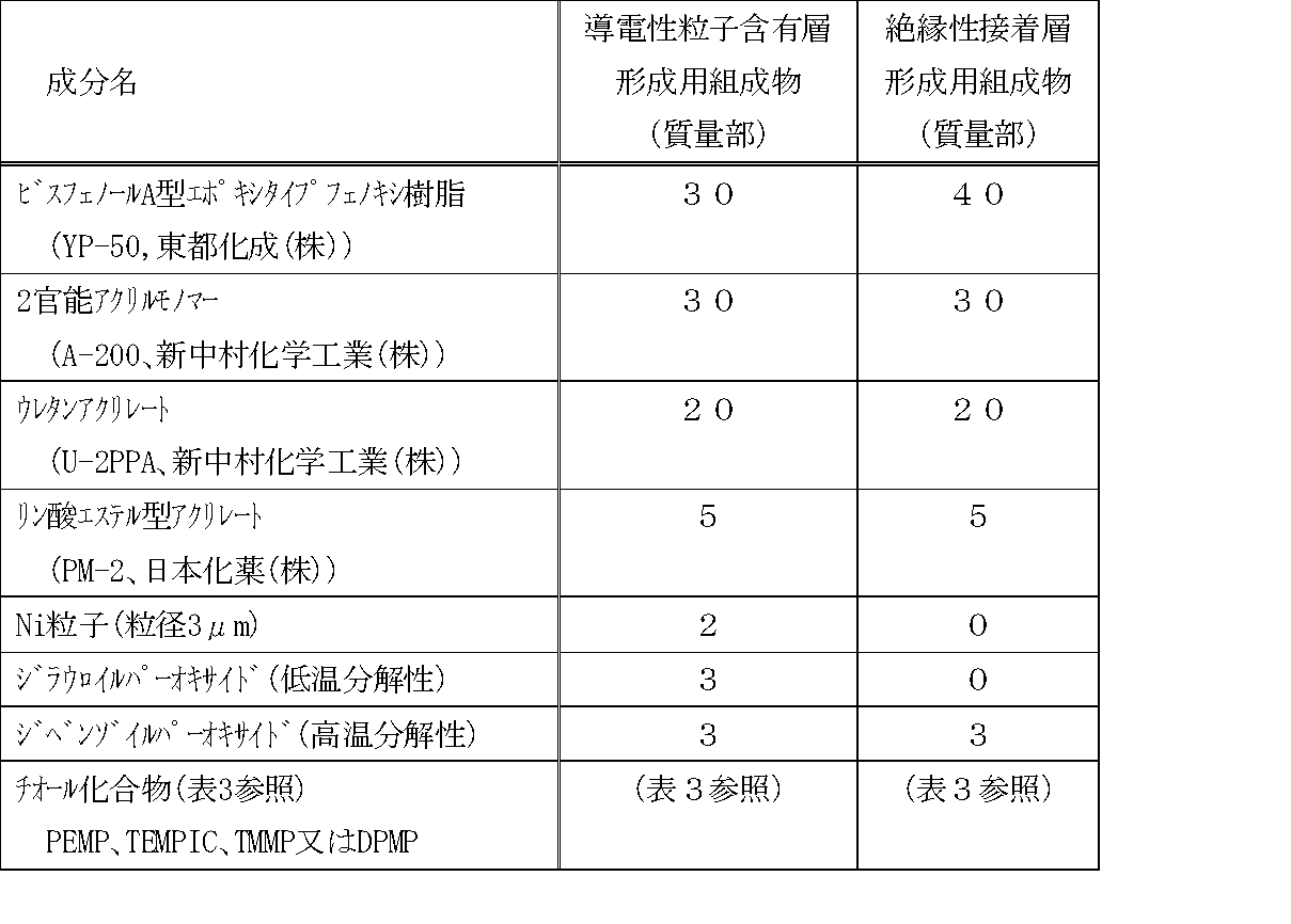
- composition for forming a conductive particle and the composition for forming an insulating adhesive layer were prepared by uniformly mixing the blended compositions shown in Table 2 by a conventional method. Subsequently, the composition for forming an insulating adhesive layer is applied to the release-treated polyester film with a bar coater so that the dry thickness is 18 ⁇ m, and dried by blowing hot air at 70 ° C. for 5 minutes. Formed. Next, the conductive particle-containing layer forming composition is applied onto the insulating adhesive layer with a bar coater so as to have a dry thickness of 17 ⁇ m, and dried by blowing hot air at 70 ° C. for 5 minutes. A conductive particle-containing layer was formed. Thereby, an anisotropic conductive film was obtained.
- connection structure is formed using the anisotropic conductive film. Produced.
- connection structure An anisotropic conductive film is placed on a printed wiring board (PWB) in which wiring of 200 ⁇ m pitch is formed on a 35 ⁇ m thick copper foil on the surface of a glass epoxy substrate so that the conductive particle-containing layer side is on the PWB side. , 80 ° C., 1 MPa, 2 seconds, heat-pressed, peeled off the peeled PET film, and temporarily bonded the anisotropic conductive film to the PWB surface.
- PWB printed wiring board
- a copper wiring portion of a COF substrate (a wiring substrate in which a copper wiring with a thickness of 8 ⁇ m with a pitch of 200 ⁇ m is formed on a polyimide film with a thickness of 38 ⁇ m) is placed, and 130 ° C., 3 MPa, 3 seconds or 190
- the connection structure for evaluation was obtained by pressure bonding under the conditions of 3 ° C. and 5 seconds.
- connection strength test> Using a peel tester (A & D Co., Ltd.), the PWB of the obtained connection structure was subjected to a 90 degree peel test (JIS K6854-1) at a peel rate of 50 mm / min. Peel strength was measured as adhesive strength and evaluated according to the following criteria. Practically, AA or A evaluation is desired.
- connection structure in accordance with the four-terminal method (JIS K7194), the initial conduction resistance ( ⁇ : max value) and the conduction resistance after aging after being held in a thermostatic bath at a temperature of 85 ° C. and a humidity of 85% RH for 500 hours. ( ⁇ : max value) was measured with a multimeter (product number 34401A, Agilent) and evaluated according to the following criteria. Practically, it is desirable that the evaluation is B at the worst both in the initial stage and after the aging.
- the anisotropic conductive films of Examples 1 to 12 in which the thiol compound is blended in both the conductive particle-containing layer and the insulating adhesive layer are practically preferable in terms of adhesive strength and connection reliability. Results are shown.
- the anisotropic conductive films of Comparative Examples 1 to 6 in which no thiol compound was blended in at least one of the conductive particle-containing layer and the insulating adhesive layer had a problem in connection reliability.
- connection reliability after aging of the anisotropic conductive film of Example 1 is “B” evaluation is that the amount of the thiol compound blended in each of the conductive particle-containing layer and the insulating adhesive layer is relatively high. This is probably because there are few.
- the anisotropic conductive film of the present invention comprises a polymerizable acrylic compound, a film-forming resin, a polymerization initiator and a conductive particle-containing layer containing a polymerization initiator and a conductive particle. Since the two-layer structure in which the insulating adhesive layer containing is laminated and the thiol compound is contained in each of the two layers, the connection reliability can be improved without reducing the adhesive strength. Therefore, it is useful for highly reliable anisotropic connection of precision electronic components.
Landscapes
- Chemical & Material Sciences (AREA)
- Organic Chemistry (AREA)
- Adhesives Or Adhesive Processes (AREA)
- Non-Insulated Conductors (AREA)
- Laminated Bodies (AREA)
- Adhesive Tapes (AREA)
Abstract
Description

該絶縁性接着層及び該導電性粒子含有層が、それぞれチオール化合物を含有することを特徴とする異方性導電フィルムを提供する。
表2の配合組成をそれぞれ常法により均一に混合することにより導電性粒子含有層形成用組成物及び絶縁性接着層形成用組成物を調製した。続いて、剥離処理ポリエステルフィルムに、絶縁性接着層形成用組成物を乾燥厚が18μmとなるようにバーコーターにより塗布し、70℃の熱風を5分間吹き掛けて乾燥させることにより絶縁性接着層を形成した。次に、絶縁性接着層上に、導電性粒子含有層形成用組成物を、乾燥厚が17μmとなるようにバーコーターにより塗布し、70℃の熱風を5分間吹き掛けて乾燥させることにより導電性粒子含有層を形成した。これにより、異方性導電フィルムを得た。
PEMP: ペンタエリスリトール テトラキス(3-メルカプトプロピオネート)、SC有機化学(株)
TEMPIC: トリス-[(3-メルカプトプロピオニルオキシ)-エチル]-イソシアヌレート、SC有機化学(株)
TMMP: トリメチロールプロパン トリス(3-メルカプトプロピオネート)、SC有機化学(株)
DPMP: ジペンタエリスリトール ヘキサキス(3-メルカプトプロピオネート)、SC有機化学(株)
EHMP: 2-エチルヘキシル-3-メルカプトプロピオネート、SC有機化学(株)
EGMP-4: テトラエチレングリコールビス(3-メルカプトプロピオネート)、SC有機化学(株)
ガラスエポキシ基板表面の35μm厚の銅箔に200μmピッチの配線が形成されたプリント配線板(PWB)に対し、異方性導電フィルムを、その導電性粒子含有層側がPWB側になるように配し、80℃、1MPa、2秒という条件で加熱圧着し、剥離PETフィルムを引き剥がし、PWB表面に異方性導電フィルムを仮接着した。この異方性導電フィルムに対し、COF基板(厚さ38μmのポリイミドフィルムに200μmピッチの厚さ8μmの銅配線を形成した配線基板)の銅配線部分を載せ、130℃、3MPa、3秒又は190℃、3MPa、5秒という条件で圧着して評価用の接続構造体を得た。
得られた接続構造体のPWBに対しCOF基板を、剥離試験機((株)エー・アンド・デイ)を用いて、剥離速度50mm/分で90度剥離試験(JIS K6854-1)を行い、ピール強度を接着強度として測定し、以下の基準で評価した。実用上、AAもしくはA評価であることが望まれる。
AA: 10[N/5cm]以上
A: 7[N/5cm]以上10[N/5cm]未満
B: 5[N/5cm]以上7[N/5cm]未満
C: 5[N/5cm]未満
得られた接続構造体について、4端子法(JIS K7194)に従って初期導通抵抗(Ω:max値)と、温度85℃、湿度85%RHの恒温槽中に500時間保持した後のエージング後導通抵抗(Ω:max値)とをマルチメータ(品番34401A、Agilent社)で測定し、以下の基準で評価した。実用上、初期及びエージング後の双方において、悪くてもB評価であることが望まれる。
AA: 0.7Ω以下
A: 0.7Ωより大1.5Ω以下
B: 1.5Ωより大2Ω以下
C: 2Ωより大

Claims (11)
- 重合性アクリル系化合物、フィルム形成樹脂及び重合開始剤を含有する絶縁性接着層と、重合性アクリル系化合物、フィルム形成樹脂、重合開始剤及び導電性粒子を含有する導電性粒子含有層とが積層されてなる異方性導電フィルムにおいて、
該絶縁性接着層及び該導電性粒子含有層が、それぞれチオール化合物を含有することを特徴とする異方性導電フィルム。 - 該絶縁性接着層中及び該導電性粒子含有層中のチオール化合物の含有量が、それぞれ0.5~5質量%及び0.3~4質量%である請求項1記載の異方性導電フィルム。
- 該絶縁性接着層中のチオール化合物の含有量が、該導電性粒子含有層中のチオール化合物の含有量以上である請求項1又は2記載の異方性導電フィルム。
- 該絶縁性接着層及び該導電性粒子含有層のチオール化合物が、それぞれ独立的にペンタエリスリトール テトラキス(3-メルカプトプロピオネート)、トリス-[(3-メルカプトプロピオニルオキシ)-エチル]-イソシアヌレート、トリメチロールプロパン トリス(3-メルカプトプロピオネート)、及びジペンタエリスリトール ヘキサキス(3-メルカプトプロピオネート)からなる群より選択される化合物である請求項1~3のいずれかに記載の異方性導電フィルム。
- 該重合開始剤が、有機過酸化物である請求項1~4のいずれかに記載の異方性導電フィルム。
- 該導電性粒子含有層に含まれる重合開始剤が、一分間半減期温度の異なる2種類の有機過酸化物を含有し、該2種類の有機過酸化物のうち、一分間半減期温度の高い有機過酸化物が分解により安息香酸又はその誘導体を発生するものであり、該絶縁性接着層に含まれる重合開始剤が、一分間半減期温度の高い該有機過酸化物である請求項5記載の異方性導電フィルム。
- 該2種類の有機過酸化物のうち、一分間半減期温度の低い有機過酸化物がジラウロイルパーオキサイドであり、一分間半減期温度の高い有機過酸化物がジベンゾイルパーオキサイドである請求項6記載の異方性導電フィルム。
- 重合性アクリル系化合物が、リン酸エステル型アクリレートを含有し、フィルム形成樹脂が、ポリエステル樹脂、ポリウレタン樹脂又はフェノキシ樹脂を含有する請求項1~7のいずれかに記載の異方性導電フィルム。
- 第1の配線基板の接続部と第2の配線基板の接続部との間を、請求項1~8のいずれかに記載の異方性導電フィルムで異方性導電接続した接続構造体。
- 該第1の配線基板が、チップオンフィルム基板またはテープキャリアパッケージ基板であり、第2の配線基板がプリント配線板であり、異方性導電フィルムが請求項7記載の異方性導電フィルムであり、該異方性導電フィルムの絶縁性接着層が第1の配線基板側に配されている請求項9記載の接続構造体。
- 第1の配線基板の接続部と第2の配線基板の接続部との間に請求項1~8のいずれかに記載の異方性導電フィルムを挟持させ、一分間半減期温度の低い有機過酸化物が分解しない第1の温度で仮貼りした後、一分間半減期温度の高い有機過酸化物が分解する第2の温度で熱圧着することを特徴とする接続構造体の製造方法。
Priority Applications (3)
| Application Number | Priority Date | Filing Date | Title |
|---|---|---|---|
| US13/575,192 US20120292082A1 (en) | 2010-11-09 | 2011-09-15 | Anisotropic conductive film |
| KR1020127021190A KR101419158B1 (ko) | 2010-11-09 | 2011-09-15 | 이방성 도전 필름 |
| CN201180011341.3A CN102763283B (zh) | 2010-11-09 | 2011-09-15 | 各向异性导电膜 |
Applications Claiming Priority (2)
| Application Number | Priority Date | Filing Date | Title |
|---|---|---|---|
| JP2010-250517 | 2010-11-09 | ||
| JP2010250517A JP5565277B2 (ja) | 2010-11-09 | 2010-11-09 | 異方性導電フィルム |
Publications (1)
| Publication Number | Publication Date |
|---|---|
| WO2012063554A1 true WO2012063554A1 (ja) | 2012-05-18 |
Family
ID=43761859
Family Applications (1)
| Application Number | Title | Priority Date | Filing Date |
|---|---|---|---|
| PCT/JP2011/071074 Ceased WO2012063554A1 (ja) | 2010-11-09 | 2011-09-15 | 異方性導電フィルム |
Country Status (6)
| Country | Link |
|---|---|
| US (1) | US20120292082A1 (ja) |
| JP (1) | JP5565277B2 (ja) |
| KR (1) | KR101419158B1 (ja) |
| CN (1) | CN102763283B (ja) |
| TW (1) | TWI502045B (ja) |
| WO (1) | WO2012063554A1 (ja) |
Cited By (3)
| Publication number | Priority date | Publication date | Assignee | Title |
|---|---|---|---|---|
| WO2015133211A1 (ja) * | 2014-03-06 | 2015-09-11 | デクセリアルズ株式会社 | 接続構造体、接続構造体の製造方法、及び回路接続材料 |
| US10272598B2 (en) | 2012-08-24 | 2019-04-30 | Dexerials Corporation | Method of producing anisotropic conductive film and anisotropic conductive film |
| US11404391B2 (en) | 2012-08-24 | 2022-08-02 | Dexerials Corporation | Anisotropic conductive film and method of producing the same |
Families Citing this family (20)
| Publication number | Priority date | Publication date | Assignee | Title |
|---|---|---|---|---|
| KR20110036733A (ko) * | 2008-07-11 | 2011-04-08 | 소니 케미카루 앤드 인포메이션 디바이스 가부시키가이샤 | 이방성 도전 필름 |
| JP5840418B2 (ja) * | 2011-08-23 | 2016-01-06 | デクセリアルズ株式会社 | 導電性接着剤及び太陽電池モジュール |
| JP5877133B2 (ja) * | 2012-07-09 | 2016-03-02 | デクセリアルズ株式会社 | 太陽電池用導電性接着剤、並びに太陽電池モジュール、及びその製造方法 |
| KR101583691B1 (ko) * | 2012-10-10 | 2016-01-08 | 제일모직주식회사 | 이방 전도성 접착 조성물 및 이를 이용한 이방 전도성 필름 |
| KR101535600B1 (ko) * | 2012-11-06 | 2015-07-09 | 제일모직주식회사 | 이방성 도전 필름 및 반도체 장치 |
| JP5956362B2 (ja) | 2013-02-19 | 2016-07-27 | デクセリアルズ株式会社 | 異方性導電フィルム、接続方法、及び接合体 |
| JP6123411B2 (ja) * | 2013-03-26 | 2017-05-10 | デクセリアルズ株式会社 | 異方性導電フィルム |
| US20160155717A1 (en) * | 2013-07-31 | 2016-06-02 | Dexerials Corporation | Anisotropic conductive film and manufacturing method therefor |
| JP6292808B2 (ja) * | 2013-09-13 | 2018-03-14 | デクセリアルズ株式会社 | 接着剤、及び発光装置 |
| JP2015098575A (ja) * | 2013-10-16 | 2015-05-28 | 日立化成株式会社 | 接着剤組成物及び接続体 |
| JP6437323B2 (ja) * | 2014-02-14 | 2018-12-12 | デクセリアルズ株式会社 | 接続構造体の製造方法、及び回路接続材料 |
| EP3158578B1 (en) | 2014-07-08 | 2024-01-10 | Canon Kabushiki Kaisha | Adhesion layer composition, method for forming film by nanoimprinting, methods for manufacturing optical component, circuit board and electronic apparatus |
| JP6579309B2 (ja) * | 2015-05-01 | 2019-09-25 | 味の素株式会社 | 硬化性組成物 |
| JP6561912B2 (ja) * | 2016-05-16 | 2019-08-21 | 東亞合成株式会社 | プラスチック製フィルム又はシート用活性エネルギー線硬化型接着剤組成物 |
| PT3543306T (pt) * | 2016-11-18 | 2025-12-11 | Furukawa Electric Co Ltd | Filme de união, fita para processamento de bolachas, método de produção de corpo unido e corpo unido |
| CN114221146B (zh) * | 2016-11-30 | 2024-11-22 | 迪睿合株式会社 | 导电粒子配置膜、其制造方法、检查探头单元、导通检查方法 |
| JP7330768B2 (ja) * | 2018-06-06 | 2023-08-22 | デクセリアルズ株式会社 | 接続体の製造方法、接続方法 |
| KR102109358B1 (ko) * | 2018-07-27 | 2020-05-12 | 강원대학교산학협력단 | 바실러스 세레우스(B. cereus) 및 바실러스 튜링겐시스(B. thuringiensis) 동정용 다중 PCR 프라이머 세트 및 이를 이용한 동정방법 |
| CN117878092A (zh) * | 2022-10-11 | 2024-04-12 | 联华电子股份有限公司 | 半导体封装及其制作方法 |
| CN121628527B (zh) * | 2026-02-04 | 2026-04-03 | 苏州大学 | 一种各向异性导电胶膜及其制备方法与应用 |
Citations (3)
| Publication number | Priority date | Publication date | Assignee | Title |
|---|---|---|---|---|
| JPH10168412A (ja) * | 1996-12-10 | 1998-06-23 | Sumitomo Bakelite Co Ltd | 異方導電性接着剤 |
| JP2004241489A (ja) * | 2003-02-04 | 2004-08-26 | Sekisui Chem Co Ltd | 異方導電性光後硬化型ペースト、それを用いた電気部品の接合方法及び電気部品 |
| JP2010037539A (ja) * | 2008-07-11 | 2010-02-18 | Sony Chemical & Information Device Corp | 異方性導電フィルム |
Family Cites Families (6)
| Publication number | Priority date | Publication date | Assignee | Title |
|---|---|---|---|---|
| JP2005146044A (ja) * | 2003-11-12 | 2005-06-09 | Sumitomo Electric Ind Ltd | 異方導電性接着剤 |
| JP2005194413A (ja) * | 2004-01-08 | 2005-07-21 | Hitachi Chem Co Ltd | 回路接続用接着フィルム及び回路接続構造体 |
| JP4880533B2 (ja) * | 2007-07-03 | 2012-02-22 | ソニーケミカル&インフォメーションデバイス株式会社 | 異方性導電膜及びその製造方法、並びに接合体 |
| JP5192194B2 (ja) * | 2007-07-26 | 2013-05-08 | デクセリアルズ株式会社 | 接着フィルム |
| JP5280034B2 (ja) * | 2007-10-10 | 2013-09-04 | 日東電工株式会社 | 配線回路基板用両面粘着テープ又はシートおよび配線回路基板 |
| US8921445B2 (en) * | 2009-04-10 | 2014-12-30 | Mitsui Chemicals, Inc. | Curable adhesive compositions |
-
2010
- 2010-11-09 JP JP2010250517A patent/JP5565277B2/ja active Active
-
2011
- 2011-09-15 KR KR1020127021190A patent/KR101419158B1/ko active Active
- 2011-09-15 US US13/575,192 patent/US20120292082A1/en not_active Abandoned
- 2011-09-15 CN CN201180011341.3A patent/CN102763283B/zh active Active
- 2011-09-15 WO PCT/JP2011/071074 patent/WO2012063554A1/ja not_active Ceased
- 2011-09-21 TW TW100133895A patent/TWI502045B/zh active
Patent Citations (3)
| Publication number | Priority date | Publication date | Assignee | Title |
|---|---|---|---|---|
| JPH10168412A (ja) * | 1996-12-10 | 1998-06-23 | Sumitomo Bakelite Co Ltd | 異方導電性接着剤 |
| JP2004241489A (ja) * | 2003-02-04 | 2004-08-26 | Sekisui Chem Co Ltd | 異方導電性光後硬化型ペースト、それを用いた電気部品の接合方法及び電気部品 |
| JP2010037539A (ja) * | 2008-07-11 | 2010-02-18 | Sony Chemical & Information Device Corp | 異方性導電フィルム |
Cited By (6)
| Publication number | Priority date | Publication date | Assignee | Title |
|---|---|---|---|---|
| US10272598B2 (en) | 2012-08-24 | 2019-04-30 | Dexerials Corporation | Method of producing anisotropic conductive film and anisotropic conductive film |
| US11136476B2 (en) | 2012-08-24 | 2021-10-05 | Dexerials Corporation | Method of producing anisotropic conductive film and anisotropic conductive film |
| US11404391B2 (en) | 2012-08-24 | 2022-08-02 | Dexerials Corporation | Anisotropic conductive film and method of producing the same |
| US11784154B2 (en) | 2012-08-24 | 2023-10-10 | Dexerials Corporation | Anisotropic conductive film and method of producing the same |
| US11787976B2 (en) | 2012-08-24 | 2023-10-17 | Dexerials Corporation | Method of producing anisotropic conductive film and anisotropic conductive film |
| WO2015133211A1 (ja) * | 2014-03-06 | 2015-09-11 | デクセリアルズ株式会社 | 接続構造体、接続構造体の製造方法、及び回路接続材料 |
Also Published As
| Publication number | Publication date |
|---|---|
| KR20120113784A (ko) | 2012-10-15 |
| US20120292082A1 (en) | 2012-11-22 |
| TWI502045B (zh) | 2015-10-01 |
| CN102763283A (zh) | 2012-10-31 |
| TW201239060A (en) | 2012-10-01 |
| KR101419158B1 (ko) | 2014-07-11 |
| JP5565277B2 (ja) | 2014-08-06 |
| CN102763283B (zh) | 2015-04-08 |
| JP2011032491A (ja) | 2011-02-17 |
Similar Documents
| Publication | Publication Date | Title |
|---|---|---|
| JP5565277B2 (ja) | 異方性導電フィルム | |
| KR101615797B1 (ko) | 이방성 도전 필름 | |
| KR101098205B1 (ko) | 이방성 도전 필름 | |
| JP6231257B2 (ja) | 導電性接着剤、及び電子部品の接続方法 | |
| JP2000234083A (ja) | 異方導電性接着剤の製造方法及びその方法により製造された接着剤を用いて製作された電子機器 | |
| JP2000044905A (ja) | 異方導電性接着剤及びそれを用いた電子機器 | |
| JP2011202173A (ja) | 異方性導電フィルム及びその製造方法 | |
| JP6307294B2 (ja) | 回路接続材料、及び電子部品の製造方法 | |
| HK1175036A (en) | Anisotropic conductive film | |
| JP6231256B2 (ja) | 異方性導電接着剤、及び電子部品の接続方法 | |
| HK1154332B (en) | Anisotropic conductive film | |
| HK1135803B (en) | Anisotropic electroconductive film |
Legal Events
| Date | Code | Title | Description |
|---|---|---|---|
| WWE | Wipo information: entry into national phase |
Ref document number: 201180011341.3 Country of ref document: CN |
|
| 121 | Ep: the epo has been informed by wipo that ep was designated in this application |
Ref document number: 11839629 Country of ref document: EP Kind code of ref document: A1 |
|
| WWE | Wipo information: entry into national phase |
Ref document number: 13575192 Country of ref document: US |
|
| ENP | Entry into the national phase |
Ref document number: 20127021190 Country of ref document: KR Kind code of ref document: A |
|
| NENP | Non-entry into the national phase |
Ref country code: DE |
|
| 122 | Ep: pct application non-entry in european phase |
Ref document number: 11839629 Country of ref document: EP Kind code of ref document: A1 |