WO2012063523A1 - 分割スパッタリングターゲット及びその製造方法 - Google Patents
分割スパッタリングターゲット及びその製造方法 Download PDFInfo
- Publication number
- WO2012063523A1 WO2012063523A1 PCT/JP2011/065950 JP2011065950W WO2012063523A1 WO 2012063523 A1 WO2012063523 A1 WO 2012063523A1 JP 2011065950 W JP2011065950 W JP 2011065950W WO 2012063523 A1 WO2012063523 A1 WO 2012063523A1
- Authority
- WO
- WIPO (PCT)
- Prior art keywords
- target
- sputtering target
- ceramic powder
- ceramic
- gap
- Prior art date
- Legal status (The legal status is an assumption and is not a legal conclusion. Google has not performed a legal analysis and makes no representation as to the accuracy of the status listed.)
- Ceased
Links
Images

Classifications
-
- C—CHEMISTRY; METALLURGY
- C23—COATING METALLIC MATERIAL; COATING MATERIAL WITH METALLIC MATERIAL; CHEMICAL SURFACE TREATMENT; DIFFUSION TREATMENT OF METALLIC MATERIAL; COATING BY VACUUM EVAPORATION, BY SPUTTERING, BY ION IMPLANTATION OR BY CHEMICAL VAPOUR DEPOSITION, IN GENERAL; INHIBITING CORROSION OF METALLIC MATERIAL OR INCRUSTATION IN GENERAL
- C23C—COATING METALLIC MATERIAL; COATING MATERIAL WITH METALLIC MATERIAL; SURFACE TREATMENT OF METALLIC MATERIAL BY DIFFUSION INTO THE SURFACE, BY CHEMICAL CONVERSION OR SUBSTITUTION; COATING BY VACUUM EVAPORATION, BY SPUTTERING, BY ION IMPLANTATION OR BY CHEMICAL VAPOUR DEPOSITION, IN GENERAL
- C23C14/00—Coating by vacuum evaporation, by sputtering or by ion implantation of the coating forming material
- C23C14/22—Coating by vacuum evaporation, by sputtering or by ion implantation of the coating forming material characterised by the process of coating
- C23C14/34—Sputtering
-
- C—CHEMISTRY; METALLURGY
- C23—COATING METALLIC MATERIAL; COATING MATERIAL WITH METALLIC MATERIAL; CHEMICAL SURFACE TREATMENT; DIFFUSION TREATMENT OF METALLIC MATERIAL; COATING BY VACUUM EVAPORATION, BY SPUTTERING, BY ION IMPLANTATION OR BY CHEMICAL VAPOUR DEPOSITION, IN GENERAL; INHIBITING CORROSION OF METALLIC MATERIAL OR INCRUSTATION IN GENERAL
- C23C—COATING METALLIC MATERIAL; COATING MATERIAL WITH METALLIC MATERIAL; SURFACE TREATMENT OF METALLIC MATERIAL BY DIFFUSION INTO THE SURFACE, BY CHEMICAL CONVERSION OR SUBSTITUTION; COATING BY VACUUM EVAPORATION, BY SPUTTERING, BY ION IMPLANTATION OR BY CHEMICAL VAPOUR DEPOSITION, IN GENERAL
- C23C14/00—Coating by vacuum evaporation, by sputtering or by ion implantation of the coating forming material
- C23C14/22—Coating by vacuum evaporation, by sputtering or by ion implantation of the coating forming material characterised by the process of coating
- C23C14/34—Sputtering
- C23C14/3407—Cathode assembly for sputtering apparatus, e.g. Target
- C23C14/3414—Metallurgical or chemical aspects of target preparation, e.g. casting, powder metallurgy
-
- C—CHEMISTRY; METALLURGY
- C04—CEMENTS; CONCRETE; ARTIFICIAL STONE; CERAMICS; REFRACTORIES
- C04B—LIME, MAGNESIA; SLAG; CEMENTS; COMPOSITIONS THEREOF, e.g. MORTARS, CONCRETE OR LIKE BUILDING MATERIALS; ARTIFICIAL STONE; CERAMICS; REFRACTORIES; TREATMENT OF NATURAL STONE
- C04B35/00—Shaped ceramic products characterised by their composition; Ceramics compositions; Processing powders of inorganic compounds preparatory to the manufacturing of ceramic products
- C04B35/01—Shaped ceramic products characterised by their composition; Ceramics compositions; Processing powders of inorganic compounds preparatory to the manufacturing of ceramic products based on oxide ceramics
- C04B35/453—Shaped ceramic products characterised by their composition; Ceramics compositions; Processing powders of inorganic compounds preparatory to the manufacturing of ceramic products based on oxide ceramics based on zinc, tin, or bismuth oxides or solid solutions thereof with other oxides, e.g. zincates, stannates or bismuthates
- C04B35/457—Shaped ceramic products characterised by their composition; Ceramics compositions; Processing powders of inorganic compounds preparatory to the manufacturing of ceramic products based on oxide ceramics based on zinc, tin, or bismuth oxides or solid solutions thereof with other oxides, e.g. zincates, stannates or bismuthates based on tin oxides or stannates
-
- H—ELECTRICITY
- H01—ELECTRIC ELEMENTS
- H01J—ELECTRIC DISCHARGE TUBES OR DISCHARGE LAMPS
- H01J37/00—Discharge tubes with provision for introducing objects or material to be exposed to the discharge, e.g. for the purpose of examination or processing thereof
- H01J37/32—Gas-filled discharge tubes
- H01J37/34—Gas-filled discharge tubes operating with cathodic sputtering
- H01J37/3411—Constructional aspects of the reactor
- H01J37/3414—Targets
-
- H—ELECTRICITY
- H01—ELECTRIC ELEMENTS
- H01J—ELECTRIC DISCHARGE TUBES OR DISCHARGE LAMPS
- H01J37/00—Discharge tubes with provision for introducing objects or material to be exposed to the discharge, e.g. for the purpose of examination or processing thereof
- H01J37/32—Gas-filled discharge tubes
- H01J37/34—Gas-filled discharge tubes operating with cathodic sputtering
- H01J37/3411—Constructional aspects of the reactor
- H01J37/3414—Targets
- H01J37/3417—Arrangements
-
- H—ELECTRICITY
- H01—ELECTRIC ELEMENTS
- H01J—ELECTRIC DISCHARGE TUBES OR DISCHARGE LAMPS
- H01J37/00—Discharge tubes with provision for introducing objects or material to be exposed to the discharge, e.g. for the purpose of examination or processing thereof
- H01J37/32—Gas-filled discharge tubes
- H01J37/34—Gas-filled discharge tubes operating with cathodic sputtering
- H01J37/3411—Constructional aspects of the reactor
- H01J37/3435—Target holders (includes backing plates and endblocks)
-
- H—ELECTRICITY
- H10—SEMICONDUCTOR DEVICES; ELECTRIC SOLID-STATE DEVICES NOT OTHERWISE PROVIDED FOR
- H10P—GENERIC PROCESSES OR APPARATUS FOR THE MANUFACTURE OR TREATMENT OF DEVICES COVERED BY CLASS H10
- H10P14/00—Formation of materials, e.g. in the shape of layers or pillars
- H10P14/20—Formation of materials, e.g. in the shape of layers or pillars of semiconductor materials
- H10P14/22—Formation of materials, e.g. in the shape of layers or pillars of semiconductor materials using physical deposition, e.g. vacuum deposition or sputtering
-
- H—ELECTRICITY
- H10—SEMICONDUCTOR DEVICES; ELECTRIC SOLID-STATE DEVICES NOT OTHERWISE PROVIDED FOR
- H10P—GENERIC PROCESSES OR APPARATUS FOR THE MANUFACTURE OR TREATMENT OF DEVICES COVERED BY CLASS H10
- H10P14/00—Formation of materials, e.g. in the shape of layers or pillars
- H10P14/20—Formation of materials, e.g. in the shape of layers or pillars of semiconductor materials
- H10P14/34—Deposited materials, e.g. layers
- H10P14/3402—Deposited materials, e.g. layers characterised by the chemical composition
- H10P14/3436—Deposited materials, e.g. layers characterised by the chemical composition being chalcogenide semiconductor materials not being oxides, e.g. ternary compounds
Definitions
- the present invention relates to a split sputtering target obtained by joining a plurality of target members, and more particularly to a split sputtering target suitable when the target member is made of an oxide semiconductor.
- a sputtering method has been widely used in manufacturing electronic parts such as information equipment, AV equipment, and home appliances.
- a display device such as a liquid crystal display device has a semiconductor such as a thin film transistor (abbreviation: TFT).
- TFT thin film transistor
- the element is formed by a sputtering method. This is because the sputtering method is extremely effective as a method for forming a thin film constituting a transparent electrode layer or the like with a large area and high accuracy.
- an oxide semiconductor typified by IGZO In—Ga—Zn—O
- IGZO In—Ga—Zn—O
- a sputtering target of an oxide semiconductor used for sputtering since the material is ceramic, it is difficult to configure a large-area target with a single target member. Therefore, a large-area oxide semiconductor sputtering target is manufactured by preparing a plurality of oxide semiconductor target members having a certain size and bonding them onto a backing plate having a desired area (for example, Patent Documents). 1).
- a Cu backing plate is usually used, and a low-melting-point solder having good thermal conductivity, for example, an In-based metal is used for joining the backing plate and the target member.
- a low-melting-point solder having good thermal conductivity for example, an In-based metal is used for joining the backing plate and the target member.
- a large-area Cu backing plate is prepared, the backing plate surface is divided into a plurality of sections, and an oxide having an area suitable for the section A plurality of semiconductor target members are prepared. Then, a plurality of target members are arranged on the backing plate, and all target members are joined to the backing plate by using an In-based or Sn-based metal low melting point solder. In this bonding, considering the difference in thermal expansion between Cu and the oxide semiconductor, the adjacent target members are adjusted so that a gap of 0.1 mm to 1.0 mm is formed at room temperature. Has been.
- a backing is formed from the gap between the target members during the sputtering process.
- Cu which is a constituent material of the plate, is also sputtered and mixed into the oxide semiconductor thin film to be formed.
- Cu in the thin film has a mixing amount of several ppm level, but its influence is extremely large for the oxide semiconductor.
- the field effect mobility in the TFT element characteristics corresponds to the gap between the target members.
- the present invention has been made in the background as described above, and is a sputtering target having a large area, and a backing plate obtained by sputtering a split sputtering target obtained by joining a plurality of target members.
- An object of the present invention is to propose a split sputtering target capable of effectively preventing the constituent materials of the above from being mixed into a thin film to be formed.
- the present invention provides a split sputtering target formed by bonding a plurality of target members on a backing plate with a low melting point solder, and a ceramic formed in a gap formed between the bonded target members.
- the material or organic material was filled.
- the ceramic material or organic material filled in the gap is fixed to the bottom of the gap.
- the split sputtering target is a plate-like or cylindrical one.
- the plate-like sputtering target is a target in which a plurality of plate-like target members having a square surface are arranged on a plate-like backing plate and bonded together.
- the cylindrical sputtering target is a cylindrical backing plate having a plurality of cylindrical target members (hollow cylinders) penetrated and arranged in a multi-stage shape in the column axis direction of the cylindrical backing plate, or A target is obtained by joining a plurality of curved target members obtained by vertically dividing a hollow cylinder in the cylinder axis direction to the outer surface of the cylindrical backing plate in the circumferential direction.
- This plate-shaped or cylindrical divided sputtering target is frequently used in a large-area sputtering apparatus.
- the present invention is intended for plate-like and cylindrical shapes, it does not prevent application to other shapes of the split sputtering target, and the shape of the target member is not limited.
- the composition of the target member can also be applied to oxide semiconductors such as IGZO and ZTO, transparent electrodes (ITO), and the like, and the composition of the target member is not limited.
- the ceramic material in the present invention is preferably a ceramic powder having the same composition as the target member.
- the gap is filled with ceramic powder having the same composition as the target member, it is possible to effectively prevent the constituent material of the backing plate from being sputtered, and even if a sputtering phenomenon occurs in the gap, the thin film is formed. This is because there is little influence.
- the organic material in the present invention is preferably a high resistance substance.
- the gap formed between the bonded target members is filled with an organic material that is a high-resistance substance, the sputtering phenomenon inside the gap during sputtering can be suppressed, and adverse effects on the thin film to be deposited can be prevented. Because it can.
- the organic material of such a high-resistance substance has a volume resistivity ( ⁇ ⁇ cm) of the high-resistance substance that is 10 times or more the volume resistivity of the target member.
- a liquid or gel-like organic material is injected into the gap, and then the solvent is vaporized, for example.
- the gap can be filled with an organic material.
- the volume resistance of the organic material described above is the volume resistance of the organic material in a solidified state.
- organic material in the present invention synthetic resin materials such as phenol resin, melamine resin, epoxy resin, urea resin, vinyl chloride resin, polyethylene and polypropylene, and general-purpose plastic materials such as polyethylene, polyvinyl chloride, polypropylene and polystyrene And semi-general plastic materials such as polyvinyl acetate, ABS resin, AS resin, and acrylic resin.
- engineering plastics such as polyacetal, polycarbonate, modified polyphenylene ether (PPE), and polybutylene terephthalate, and super engineering plastics such as polyarylate, polysulfone, polyphenylene sulfide, polyether ether ketone, polyimide resin, and fluororesin can also be used.
- a polyimide resin or the like is suitable for the present invention because of its high heat resistance and insulation.
- the filling thickness of the organic material is preferably 0.0001 mm to 1.0 mm.
- the filling thickness of the ceramic powder is preferably 10% to 70% of the depth of the gap formed between the target members. . If it is less than 10% of the gap depth, the effect of suppressing the sputtering of the constituent material of the backing plate tends to decrease, and if it exceeds 70%, the filled ceramic powder falls off and particles are generated during sputtering. Cause.
- This gap depth is determined by the thickness of the end of the target member or the thickness of the edge of the peripheral part of the entire manufactured sputtering target. The initial gap in which the divided sputtering target was manufactured before it was used for sputtering. Say depth.
- a packing density of the ceramic powder is 40% to 70%
- an average particle diameter D 50 of the ceramic powder is 0.5 [mu] m-8.0 .mu.m
- Ceramic powder filled in the gap for example, when it is to be filled with slurry, which was the average particle diameter D 50 of the ceramic powder is less than 0.5 [mu] m, dried by filling the slurry, solidification The cracked ceramic powder is likely to be cracked and easily fall off from the gap.
- the average particle diameter D 50 is larger than 8.0 ⁇ m, when the gap is filled as a slurry and then dried, the filling density of the ceramic powder tends to be less than 40%, and the gap is easily dropped from the gap. Therefore, when the average particle diameter D 50 of the ceramic powder is 0.5 ⁇ m to 8.0 ⁇ m, it is possible to suppress the ceramic powder filled in the gap from falling off.
- the packing density of the ceramic powder is the same as that for manufacturing the split sputtering target, and the slurry of the ceramic powder is poured into a container of a predetermined shape, for example, a cylindrical container, and the slurry is completely dried. Then, the input capacity and weight can be measured and specified.
- the ceramic powder filling density is such that the density of the target member is 100%.
- the ceramic material in the present invention may be a ceramic fiber.
- alumina and silica yarns have been supplied as ceramic fibers, and the fiber diameters are very thin. Therefore, an effect similar to that of the ceramic powder described above can be realized by filling the gaps with such ceramic fibers.
- the ceramic fiber having a fiber diameter that matches the width of the gap is pushed into the gap to cover the surface of the backing plate. can do.
- a small amount of low melting point solder such as In used for joining the backing plate and the target member is left in the gap, and the ceramic fiber can be fixed to the gap bottom using the low melting point solder.
- the ceramic material in the present invention can be applied to a ceramic (filler) dispersed in a resin.
- the oxide semiconductor is preferably made of an oxide containing at least one of In, Zn, and Ga.
- IGZO In—Ga—Zn—O
- GZO Ga—Zn—O
- IZO In—Zn—O
- ZnO ZnO
- the oxide semiconductor includes at least one of Sn, Ti, Ba, Ca, Zn, Mg, Ge, Y, La, Al, Si, and Ga. It is preferable to consist of the oxide which contains. Specifically, Sn—Ba—O, Sn—Zn—O, Sn—Ti—O, Sn—Ca—O, Sn—Mg—O, Zn—Mg—O, Zn—Ge—O, Zn—Ca -O, Zn-Sn-Ge-O, or an oxide in which Ge of these oxides is changed to Mg, Y, La, Al, Si, or Ga can be given.
- the oxide semiconductor consists of an oxide containing any 1 or more types of Cu, Al, Ga, and In. Specific examples include Cu 2 O, CuAlO 2 , CuGaO 2 , and CuInO 2 .
- a gap formed between bonded target members is filled with a fluid containing ceramic powder having the same composition as the target member, dried, and then irradiated with laser or infrared rays. It can be realized by sintering the ceramic powder.
- the fluid containing ceramic powder in the present invention can be prepared by mixing a predetermined amount of ceramic powder having the same composition as the target member using an appropriate solvent.
- a predetermined amount of each of In 2 O 3 , Ga 2 O 3 , and ZnO powder raw materials is put into a 5 L polypot, and water and a dispersant (carboxylic acid) are added.
- Ammonia is added, a predetermined amount of ⁇ 10 mmZr ball media is put into a polypot, and a fluid is prepared by ball mill stirring and mixing at a peripheral speed of 50 rpm for 10 hours.
- the powder raw material is preferably adjusted to a powder having a BET value of about 3 m 2 / g to 20 m 2 / g.
- the powder raw material can be used as it is, but it is also possible to use a powder that has been subjected to a calcination treatment at 700 ° C. to 1300 ° C.
- water and the dispersant are mixed at 10% to 15% by mass of water and 0.25% to 0.5% by mass of the dispersant. It is preferable.
- the filled portion is irradiated with a laser.
- the wavelength is 308 nm
- the frequency is 100 Hz
- the pulse width is 30 ns
- the energy density is 100 mJ / cm 2 to 1000 mJ / cm 2.
- the laser irradiation is performed, the outermost surface side of the ceramic powder filled in the gap is sintered.
- sputtering prevents the constituent material of the backing plate from being mixed into the thin film to be formed. be able to.
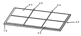
- the split sputtering target in this embodiment includes an oxygen-free copper backing plate 10 (thickness 10 mm, length 630 mm, width 710 mm) and six IGZO target members 20 (thickness 6 mm, length 210 mm, 355 mm in width). In was used as the low melting point solder for bonding. The gap 30 between the target members was 0.5 mm.
- the target member made from IGZO weighed each raw material powder of In 2 O 3 , Ga 2 O 3 , and ZnO at a ratio of 1 mol: 1 mol: 2 mol, and mixed with a ball mill for 20 hours. And after adding and mixing 8 mass% of polyvinyl alcohol aqueous solution diluted to 4 mass% as a binder with respect to the powder total amount, it shape
- the six target members thus fabricated were arranged and joined as shown in FIG. 1 using In low melting point solder.
- both the backing plate and the target member are heated to 200 ° C.
- the molten low melting point solder (In) is applied to the surface of the backing plate
- the target member is placed on the low melting point solder, and the room temperature is reached. This was done by cooling.
- a spacer of a heat-resistant material was interposed at a position corresponding to the gap formed between the target members so as to prevent the low melting point solder from entering the gap portion.
- a fluid of IGZO ceramic powder was prepared.
- Each powder raw material of In 2 O 3 (138.8 g), Ga 2 O 3 (93.7 g), ZnO (81.4 g) is put into a 5 L polypot, and water and a dispersant (ammonium carboxylate) are added.
- a fluid was prepared by putting a predetermined amount of ⁇ 10 mmZr ball media into a polypot and performing ball mill stirring and mixing for 10 hours. Water and dispersant were 16%: 0.25% of water: dispersant with respect to the total amount of powder to be charged.
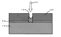
- the prepared ceramic powder fluid 100 was injected into the gap 30 between the target members using a syringe. The injection amount at this time was 50% of the target member thickness. Thereafter, drying treatment was performed at 70 ° C. to 120 ° C. in the atmosphere, and the injected fluid was dried.
- the dried fluid 100 in the gap 30 between the target members was irradiated with laser.
- the laser irradiation conditions were a wavelength of 308 nm, a frequency of 100 Hz, a pulse width of 30 ns, an energy density of 500 mJ / cm 2, and the outermost surface side of the ceramic powder filled in the gap was sintered. After this laser treatment, no falling off of the ceramic powder filled from the split sputtering target was confirmed.
- the packing density of the ceramic powder was calculated by pouring the above-mentioned ceramic powder fluid into a cylindrical container of ⁇ 20 mm, completely drying the fluid, and measuring its input capacity and weight. 60%.
- the average particle size of the ceramic powder was 0.6 ⁇ m.
- the sputtering evaluation test was performed on the divided sputtering target in which the gap between the target members was filled with the ceramic powder.
- a sputtering apparatus (SMD-450B, manufactured by ULVAC) was used to form an IGZO thin film having a thickness of 14 ⁇ m on a non-alkali glass substrate (370 mm ⁇ 470 mm ⁇ 0.7 mm thickness: manufactured by Nippon Electric Glass).
- the sputtering conditions were Ar 100 cc, O 2 10 cc, sputtering pressure 0.7 Pa, and power 4.3 kW.
- the substrate immediately above corresponding to the gap portion of the split sputtering target and the substrate other than the gap portion were cut out.
- the cut substrate was subjected to sputter evaluation by measuring the amount of Cu mixed in the IGZO thin film by atomic absorption analysis.
- a sputter evaluation test was similarly performed on a split sputtering target in which the gap portion was not filled with ceramic powder.
- the amount of Cu mixed into the IGZO thin film was less than 2 ppm (below the detection limit of atomic absorption analysis).
- the amount of Cu mixed into the IGZO thin film was 19 ppm.
- the present invention can effectively prevent impurities from being mixed during sputtering when a thin film is formed using a large-area divided sputtering target.
Landscapes
- Chemical & Material Sciences (AREA)
- Engineering & Computer Science (AREA)
- Organic Chemistry (AREA)
- Materials Engineering (AREA)
- Physics & Mathematics (AREA)
- Plasma & Fusion (AREA)
- Analytical Chemistry (AREA)
- Mechanical Engineering (AREA)
- Metallurgy (AREA)
- Chemical Kinetics & Catalysis (AREA)
- Ceramic Engineering (AREA)
- Manufacturing & Machinery (AREA)
- Structural Engineering (AREA)
- Physical Vapour Deposition (AREA)
- Physical Deposition Of Substances That Are Components Of Semiconductor Devices (AREA)
Abstract
Description
20 ターゲット部材
30 間隙
50 低融点ハンダ
100 セラミック粉(流動体)
Claims (7)
- バッキングプレート上に、複数のターゲット部材を低融点ハンダにより接合して形成される分割スパッタリングターゲットにおいて、
接合されたターゲット部材間に形成された間隙に、セラミック材または有機材料が充填されていることを特徴とする分割スパッタリングターゲット。 - セラミック材が、ターゲット部材と同組成のセラミック粉である請求項1に記載の分割スパッタリングターゲット。
- 有機材料は、高抵抗物質である請求項1に記載の分割スパッタリングターゲット。
- セラミック粉の充填厚さは、ターゲット部材間に形成された間隙深さの10%~70%である請求項2に記載の分割スパッタリングターゲット。
- セラミック粉の充填密度が40%~70%であり、セラミック粉の平均粒径D50が0.5μm~8.0μmである請求項2または請求項4に記載の分割スパッタリングターゲット。
- セラミック材が、セラミック繊維である請求項1に記載の分割スパッタリングターゲット。
- バッキングプレート上に、複数のターゲット部材を低融点ハンダにより接合して形成される分割スパッタリングターゲットの製造方法において、
接合されたターゲット部材の間に形成された間隙に、該ターゲット部材と同組成のセラミック粉を含む流動体を充填して乾燥した後、
充填部分にレーザーまたは赤外線を照射してセラミック粉を焼結することを特徴とする分割スパッタリングターゲットの製造方法。
Priority Applications (4)
| Application Number | Priority Date | Filing Date | Title |
|---|---|---|---|
| CN201180005296.0A CN102686766B (zh) | 2010-11-08 | 2011-07-13 | 分割溅镀靶及其制造方法 |
| JP2012503150A JP4961513B1 (ja) | 2010-11-08 | 2011-07-13 | 分割スパッタリングターゲット及びその製造方法 |
| KR1020127016052A KR101191817B1 (ko) | 2010-11-08 | 2011-07-13 | 분할 스퍼터링 타깃 및 그 제조 방법 |
| TW100126731A TWI375728B (en) | 2010-11-08 | 2011-07-28 | Divided sputtering target and method of producing the same |
Applications Claiming Priority (2)
| Application Number | Priority Date | Filing Date | Title |
|---|---|---|---|
| JP2010-249779 | 2010-11-08 | ||
| JP2010249779 | 2010-11-08 |
Publications (1)
| Publication Number | Publication Date |
|---|---|
| WO2012063523A1 true WO2012063523A1 (ja) | 2012-05-18 |
Family
ID=46050682
Family Applications (1)
| Application Number | Title | Priority Date | Filing Date |
|---|---|---|---|
| PCT/JP2011/065950 Ceased WO2012063523A1 (ja) | 2010-11-08 | 2011-07-13 | 分割スパッタリングターゲット及びその製造方法 |
Country Status (5)
| Country | Link |
|---|---|
| JP (1) | JP4961513B1 (ja) |
| KR (1) | KR101191817B1 (ja) |
| CN (1) | CN102686766B (ja) |
| TW (1) | TWI375728B (ja) |
| WO (1) | WO2012063523A1 (ja) |
Cited By (7)
| Publication number | Priority date | Publication date | Assignee | Title |
|---|---|---|---|---|
| US20140110249A1 (en) * | 2011-03-04 | 2014-04-24 | Sharp Kabushiki Kaisha | Sputtering target, method for manufacturing same, and method for manufacturing thin film transistor |
| WO2014131458A1 (en) * | 2013-02-28 | 2014-09-04 | Applied Materials, Inc. | Gapless rotary target and method of manufacturing thereof |
| JP2015059268A (ja) * | 2013-09-20 | 2015-03-30 | 東ソー株式会社 | 平板形スパッタリングターゲットとその製造方法 |
| JP2015059269A (ja) * | 2013-09-20 | 2015-03-30 | 東ソー株式会社 | 円筒形スパッタリングターゲットとその製造方法 |
| KR20180129769A (ko) | 2016-03-28 | 2018-12-05 | 미쓰이금속광업주식회사 | 스퍼터링 타깃재 및 그의 제조 방법, 및 스퍼터링 타깃 |
| JPWO2021024896A1 (ja) * | 2019-08-08 | 2021-02-11 | ||
| KR20220139301A (ko) | 2020-02-06 | 2022-10-14 | 미쓰이금속광업주식회사 | 스퍼터링 타깃 |
Families Citing this family (1)
| Publication number | Priority date | Publication date | Assignee | Title |
|---|---|---|---|---|
| JP7311290B2 (ja) | 2019-03-27 | 2023-07-19 | Jx金属株式会社 | 分割スパッタリングターゲット及びその製造方法 |
Citations (2)
| Publication number | Priority date | Publication date | Assignee | Title |
|---|---|---|---|---|
| JPS5920470A (ja) * | 1982-07-26 | 1984-02-02 | Murata Mfg Co Ltd | スパツタリング用タ−ゲツト |
| JPH10121232A (ja) * | 1996-10-14 | 1998-05-12 | Mitsubishi Chem Corp | スパッタリングターゲット |
Family Cites Families (2)
| Publication number | Priority date | Publication date | Assignee | Title |
|---|---|---|---|---|
| CN1029525C (zh) * | 1990-11-29 | 1995-08-16 | 中国科学院计算技术研究所 | 真空溅射系统阴极靶的粘接方法 |
| JP2005232580A (ja) | 2004-02-23 | 2005-09-02 | Toyoshima Seisakusho:Kk | 分割スパッタリングターゲット |
-
2011
- 2011-07-13 CN CN201180005296.0A patent/CN102686766B/zh active Active
- 2011-07-13 JP JP2012503150A patent/JP4961513B1/ja active Active
- 2011-07-13 KR KR1020127016052A patent/KR101191817B1/ko active Active
- 2011-07-13 WO PCT/JP2011/065950 patent/WO2012063523A1/ja not_active Ceased
- 2011-07-28 TW TW100126731A patent/TWI375728B/zh active
Patent Citations (2)
| Publication number | Priority date | Publication date | Assignee | Title |
|---|---|---|---|---|
| JPS5920470A (ja) * | 1982-07-26 | 1984-02-02 | Murata Mfg Co Ltd | スパツタリング用タ−ゲツト |
| JPH10121232A (ja) * | 1996-10-14 | 1998-05-12 | Mitsubishi Chem Corp | スパッタリングターゲット |
Cited By (8)
| Publication number | Priority date | Publication date | Assignee | Title |
|---|---|---|---|---|
| US20140110249A1 (en) * | 2011-03-04 | 2014-04-24 | Sharp Kabushiki Kaisha | Sputtering target, method for manufacturing same, and method for manufacturing thin film transistor |
| WO2014131458A1 (en) * | 2013-02-28 | 2014-09-04 | Applied Materials, Inc. | Gapless rotary target and method of manufacturing thereof |
| JP2015059268A (ja) * | 2013-09-20 | 2015-03-30 | 東ソー株式会社 | 平板形スパッタリングターゲットとその製造方法 |
| JP2015059269A (ja) * | 2013-09-20 | 2015-03-30 | 東ソー株式会社 | 円筒形スパッタリングターゲットとその製造方法 |
| KR20180129769A (ko) | 2016-03-28 | 2018-12-05 | 미쓰이금속광업주식회사 | 스퍼터링 타깃재 및 그의 제조 방법, 및 스퍼터링 타깃 |
| JPWO2021024896A1 (ja) * | 2019-08-08 | 2021-02-11 | ||
| JP7419379B2 (ja) | 2019-08-08 | 2024-01-22 | 三井金属鉱業株式会社 | 分割スパッタリングターゲット |
| KR20220139301A (ko) | 2020-02-06 | 2022-10-14 | 미쓰이금속광업주식회사 | 스퍼터링 타깃 |
Also Published As
| Publication number | Publication date |
|---|---|
| JP4961513B1 (ja) | 2012-06-27 |
| TWI375728B (en) | 2012-11-01 |
| KR101191817B1 (ko) | 2012-10-16 |
| CN102686766A (zh) | 2012-09-19 |
| TW201219589A (en) | 2012-05-16 |
| KR20120086730A (ko) | 2012-08-03 |
| CN102686766B (zh) | 2014-04-09 |
| JPWO2012063523A1 (ja) | 2014-05-12 |
Similar Documents
| Publication | Publication Date | Title |
|---|---|---|
| JP4961513B1 (ja) | 分割スパッタリングターゲット及びその製造方法 | |
| JP5711172B2 (ja) | 分割スパッタリングターゲット及びその製造方法 | |
| TW201029952A (en) | Composite oxide sintered body and sputtering target comprising same | |
| JP4961515B1 (ja) | 分割スパッタリングターゲット及びその製造方法 | |
| CN104278240A (zh) | 溅射靶、其制造方法、用其生产有机发光显示设备的方法 | |
| Umar et al. | Substrate temperature effects on the structural, compositional, and electrical properties of VO2 thin films deposited by pulsed laser deposition | |
| Hamdelou et al. | The effect of the starting powders particle size on the electrical properties of sintered Co doped ZnO varistors | |
| CN102167579A (zh) | 一种低温烧结的ZnO-Bi2O3-B2O3系压敏电阻材料及其制备方法 | |
| US9416439B2 (en) | Sputtering target, method of fabricating the same, and method of fabricating an organic light emitting display apparatus | |
| CN103602942B (zh) | 耐高温涂层涂覆坩埚表面保护贵金属坩埚的方法 | |
| Roy et al. | Effect of thermochemical synthetic conditions on the structure and dielectric properties of Ga1. 9Fe0. 1O3 compounds | |
| Zhang et al. | Polarization‐Driven Energy Storage Enhancement in KNN‐Based Relaxor Ceramics under Moderate Electric Field | |
| CN103922736B (zh) | 铌酸钾基v型ptc材料及其制备方法 | |
| TW201816156A (zh) | 氧化物燒結體及濺鍍靶材 | |
| CN104810475A (zh) | 一种纳米复合TiO2-Sb2Te相变存储薄膜材料及其制备方法 | |
| Chang et al. | Crystallization behaviors of an ultra-thin Ga–Sb film | |
| CN114008237A (zh) | 溅射靶及溅射靶的制造方法 | |
| Liu et al. | Effect of gallium doping on the properties of GZO target | |
| Wang et al. | Fabrication of high performance multilayer ZnO varistors with chemically synthesized doped zinc oxide powder | |
| Wang et al. | B2O3-doped ZnO-Pr6O11 based varistor ceramics | |
| Muchira et al. | Crystallization kinetics of In40Se60 thin films for phase change random access memory (PRAM) applications | |
| Mansor et al. | Characteristics of Humidity Sensor Fabricated Using Nanostructured ZnO Thin Film by Sol-Gel Method | |
| JP2020164957A (ja) | スパッタリングターゲットおよび、スパッタリングターゲットの製造方法 | |
| Zhen et al. | Enhanced humidity stability of (Li, K, Na) NbO3-based lead-free piezoelectric ceramics by adding B2O3 | |
| JP2013177262A (ja) | 酸化物焼結体およびその製造方法 |
Legal Events
| Date | Code | Title | Description |
|---|---|---|---|
| WWE | Wipo information: entry into national phase |
Ref document number: 201180005296.0 Country of ref document: CN |
|
| WWE | Wipo information: entry into national phase |
Ref document number: 2012503150 Country of ref document: JP |
|
| ENP | Entry into the national phase |
Ref document number: 20127016052 Country of ref document: KR Kind code of ref document: A |
|
| 121 | Ep: the epo has been informed by wipo that ep was designated in this application |
Ref document number: 11840106 Country of ref document: EP Kind code of ref document: A1 |
|
| NENP | Non-entry into the national phase |
Ref country code: DE |
|
| 122 | Ep: pct application non-entry in european phase |
Ref document number: 11840106 Country of ref document: EP Kind code of ref document: A1 |