WO2012060223A1 - 半導体装置およびその製造方法 - Google Patents
半導体装置およびその製造方法 Download PDFInfo
- Publication number
- WO2012060223A1 WO2012060223A1 PCT/JP2011/073996 JP2011073996W WO2012060223A1 WO 2012060223 A1 WO2012060223 A1 WO 2012060223A1 JP 2011073996 W JP2011073996 W JP 2011073996W WO 2012060223 A1 WO2012060223 A1 WO 2012060223A1
- Authority
- WO
- WIPO (PCT)
- Prior art keywords
- gate insulating
- film
- insulating film
- electrode
- region
- Prior art date
Links
- 239000004065 semiconductor Substances 0.000 title claims abstract description 29
- 238000004519 manufacturing process Methods 0.000 title claims description 22
- 229910010271 silicon carbide Inorganic materials 0.000 claims abstract description 71
- 239000000758 substrate Substances 0.000 claims abstract description 69
- HBMJWWWQQXIZIP-UHFFFAOYSA-N silicon carbide Chemical compound [Si+]#[C-] HBMJWWWQQXIZIP-UHFFFAOYSA-N 0.000 claims abstract description 51
- 229910045601 alloy Inorganic materials 0.000 claims abstract description 8
- 239000000956 alloy Substances 0.000 claims abstract description 8
- VYPSYNLAJGMNEJ-UHFFFAOYSA-N Silicium dioxide Chemical compound O=[Si]=O VYPSYNLAJGMNEJ-UHFFFAOYSA-N 0.000 claims description 42
- 238000000137 annealing Methods 0.000 claims description 19
- 235000012239 silicon dioxide Nutrition 0.000 claims description 16
- 239000000377 silicon dioxide Substances 0.000 claims description 16
- 238000000034 method Methods 0.000 claims description 15
- 229910052814 silicon oxide Inorganic materials 0.000 claims description 11
- 229910052719 titanium Inorganic materials 0.000 claims description 10
- 238000009413 insulation Methods 0.000 abstract 5
- 239000010936 titanium Substances 0.000 description 26
- 239000012535 impurity Substances 0.000 description 24
- 229910052782 aluminium Inorganic materials 0.000 description 13
- 238000009792 diffusion process Methods 0.000 description 12
- 238000002161 passivation Methods 0.000 description 8
- 229910004298 SiO 2 Inorganic materials 0.000 description 7
- 229910052710 silicon Inorganic materials 0.000 description 7
- 238000010292 electrical insulation Methods 0.000 description 6
- 238000010438 heat treatment Methods 0.000 description 6
- 229910052796 boron Inorganic materials 0.000 description 5
- 238000005468 ion implantation Methods 0.000 description 5
- 239000000463 material Substances 0.000 description 5
- 230000003287 optical effect Effects 0.000 description 5
- IJGRMHOSHXDMSA-UHFFFAOYSA-N Atomic nitrogen Chemical compound N#N IJGRMHOSHXDMSA-UHFFFAOYSA-N 0.000 description 4
- 230000015572 biosynthetic process Effects 0.000 description 4
- 239000004020 conductor Substances 0.000 description 4
- 229910021420 polycrystalline silicon Inorganic materials 0.000 description 4
- 229920005591 polysilicon Polymers 0.000 description 4
- RTAQQCXQSZGOHL-UHFFFAOYSA-N Titanium Chemical compound [Ti] RTAQQCXQSZGOHL-UHFFFAOYSA-N 0.000 description 3
- 238000005275 alloying Methods 0.000 description 3
- 229910052799 carbon Inorganic materials 0.000 description 3
- 238000005229 chemical vapour deposition Methods 0.000 description 3
- 239000007789 gas Substances 0.000 description 3
- 239000011261 inert gas Substances 0.000 description 3
- 238000001020 plasma etching Methods 0.000 description 3
- XKRFYHLGVUSROY-UHFFFAOYSA-N Argon Chemical compound [Ar] XKRFYHLGVUSROY-UHFFFAOYSA-N 0.000 description 2
- ATUOYWHBWRKTHZ-UHFFFAOYSA-N Propane Chemical compound CCC ATUOYWHBWRKTHZ-UHFFFAOYSA-N 0.000 description 2
- 238000010521 absorption reaction Methods 0.000 description 2
- 230000004913 activation Effects 0.000 description 2
- XAGFODPZIPBFFR-UHFFFAOYSA-N aluminium Chemical compound [Al] XAGFODPZIPBFFR-UHFFFAOYSA-N 0.000 description 2
- 238000004458 analytical method Methods 0.000 description 2
- QVGXLLKOCUKJST-UHFFFAOYSA-N atomic oxygen Chemical compound [O] QVGXLLKOCUKJST-UHFFFAOYSA-N 0.000 description 2
- 229910052757 nitrogen Inorganic materials 0.000 description 2
- 239000001301 oxygen Substances 0.000 description 2
- 229910052760 oxygen Inorganic materials 0.000 description 2
- ZOXJGFHDIHLPTG-UHFFFAOYSA-N Boron Chemical compound [B] ZOXJGFHDIHLPTG-UHFFFAOYSA-N 0.000 description 1
- OKTJSMMVPCPJKN-UHFFFAOYSA-N Carbon Chemical compound [C] OKTJSMMVPCPJKN-UHFFFAOYSA-N 0.000 description 1
- UFHFLCQGNIYNRP-UHFFFAOYSA-N Hydrogen Chemical compound [H][H] UFHFLCQGNIYNRP-UHFFFAOYSA-N 0.000 description 1
- OAICVXFJPJFONN-UHFFFAOYSA-N Phosphorus Chemical compound [P] OAICVXFJPJFONN-UHFFFAOYSA-N 0.000 description 1
- BLRPTPMANUNPDV-UHFFFAOYSA-N Silane Chemical compound [SiH4] BLRPTPMANUNPDV-UHFFFAOYSA-N 0.000 description 1
- XUIMIQQOPSSXEZ-UHFFFAOYSA-N Silicon Chemical compound [Si] XUIMIQQOPSSXEZ-UHFFFAOYSA-N 0.000 description 1
- 238000002441 X-ray diffraction Methods 0.000 description 1
- AZDRQVAHHNSJOQ-UHFFFAOYSA-N alumane Chemical group [AlH3] AZDRQVAHHNSJOQ-UHFFFAOYSA-N 0.000 description 1
- 229910052786 argon Inorganic materials 0.000 description 1
- 230000008020 evaporation Effects 0.000 description 1
- 238000001704 evaporation Methods 0.000 description 1
- 230000005669 field effect Effects 0.000 description 1
- 239000001257 hydrogen Substances 0.000 description 1
- 229910052739 hydrogen Inorganic materials 0.000 description 1
- 150000002500 ions Chemical class 0.000 description 1
- 229910044991 metal oxide Inorganic materials 0.000 description 1
- 150000004706 metal oxides Chemical class 0.000 description 1
- 239000000203 mixture Substances 0.000 description 1
- 238000012986 modification Methods 0.000 description 1
- 230000004048 modification Effects 0.000 description 1
- 229910052759 nickel Inorganic materials 0.000 description 1
- 150000004767 nitrides Chemical class 0.000 description 1
- 230000003647 oxidation Effects 0.000 description 1
- 238000007254 oxidation reaction Methods 0.000 description 1
- 229910052698 phosphorus Inorganic materials 0.000 description 1
- 239000011574 phosphorus Substances 0.000 description 1
- 238000002360 preparation method Methods 0.000 description 1
- 239000001294 propane Substances 0.000 description 1
- 238000000682 scanning probe acoustic microscopy Methods 0.000 description 1
- 238000001004 secondary ion mass spectrometry Methods 0.000 description 1
- 229910000077 silane Inorganic materials 0.000 description 1
- 239000010703 silicon Substances 0.000 description 1
- 238000004544 sputter deposition Methods 0.000 description 1
Images


Classifications
-
- H—ELECTRICITY
- H01—ELECTRIC ELEMENTS
- H01L—SEMICONDUCTOR DEVICES NOT COVERED BY CLASS H10
- H01L21/00—Processes or apparatus adapted for the manufacture or treatment of semiconductor or solid state devices or of parts thereof
- H01L21/02—Manufacture or treatment of semiconductor devices or of parts thereof
- H01L21/04—Manufacture or treatment of semiconductor devices or of parts thereof the devices having potential barriers, e.g. a PN junction, depletion layer or carrier concentration layer
- H01L21/0445—Manufacture or treatment of semiconductor devices or of parts thereof the devices having potential barriers, e.g. a PN junction, depletion layer or carrier concentration layer the devices having semiconductor bodies comprising crystalline silicon carbide
- H01L21/048—Making electrodes
- H01L21/0485—Ohmic electrodes
-
- H—ELECTRICITY
- H10—SEMICONDUCTOR DEVICES; ELECTRIC SOLID-STATE DEVICES NOT OTHERWISE PROVIDED FOR
- H10D—INORGANIC ELECTRIC SEMICONDUCTOR DEVICES
- H10D12/00—Bipolar devices controlled by the field effect, e.g. insulated-gate bipolar transistors [IGBT]
- H10D12/01—Manufacture or treatment
- H10D12/031—Manufacture or treatment of IGBTs
-
- H—ELECTRICITY
- H10—SEMICONDUCTOR DEVICES; ELECTRIC SOLID-STATE DEVICES NOT OTHERWISE PROVIDED FOR
- H10D—INORGANIC ELECTRIC SEMICONDUCTOR DEVICES
- H10D30/00—Field-effect transistors [FET]
- H10D30/01—Manufacture or treatment
-
- H—ELECTRICITY
- H10—SEMICONDUCTOR DEVICES; ELECTRIC SOLID-STATE DEVICES NOT OTHERWISE PROVIDED FOR
- H10D—INORGANIC ELECTRIC SEMICONDUCTOR DEVICES
- H10D30/00—Field-effect transistors [FET]
- H10D30/60—Insulated-gate field-effect transistors [IGFET]
- H10D30/64—Double-diffused metal-oxide semiconductor [DMOS] FETs
- H10D30/66—Vertical DMOS [VDMOS] FETs
-
- H—ELECTRICITY
- H10—SEMICONDUCTOR DEVICES; ELECTRIC SOLID-STATE DEVICES NOT OTHERWISE PROVIDED FOR
- H10D—INORGANIC ELECTRIC SEMICONDUCTOR DEVICES
- H10D62/00—Semiconductor bodies, or regions thereof, of devices having potential barriers
- H10D62/80—Semiconductor bodies, or regions thereof, of devices having potential barriers characterised by the materials
- H10D62/83—Semiconductor bodies, or regions thereof, of devices having potential barriers characterised by the materials being Group IV materials, e.g. B-doped Si or undoped Ge
- H10D62/8303—Diamond
-
- H—ELECTRICITY
- H10—SEMICONDUCTOR DEVICES; ELECTRIC SOLID-STATE DEVICES NOT OTHERWISE PROVIDED FOR
- H10D—INORGANIC ELECTRIC SEMICONDUCTOR DEVICES
- H10D62/00—Semiconductor bodies, or regions thereof, of devices having potential barriers
- H10D62/80—Semiconductor bodies, or regions thereof, of devices having potential barriers characterised by the materials
- H10D62/83—Semiconductor bodies, or regions thereof, of devices having potential barriers characterised by the materials being Group IV materials, e.g. B-doped Si or undoped Ge
- H10D62/832—Semiconductor bodies, or regions thereof, of devices having potential barriers characterised by the materials being Group IV materials, e.g. B-doped Si or undoped Ge being Group IV materials comprising two or more elements, e.g. SiGe
- H10D62/8325—Silicon carbide
-
- H—ELECTRICITY
- H10—SEMICONDUCTOR DEVICES; ELECTRIC SOLID-STATE DEVICES NOT OTHERWISE PROVIDED FOR
- H10D—INORGANIC ELECTRIC SEMICONDUCTOR DEVICES
- H10D64/00—Electrodes of devices having potential barriers
- H10D64/01—Manufacture or treatment
-
- H—ELECTRICITY
- H10—SEMICONDUCTOR DEVICES; ELECTRIC SOLID-STATE DEVICES NOT OTHERWISE PROVIDED FOR
- H10D—INORGANIC ELECTRIC SEMICONDUCTOR DEVICES
- H10D64/00—Electrodes of devices having potential barriers
- H10D64/20—Electrodes characterised by their shapes, relative sizes or dispositions
- H10D64/23—Electrodes carrying the current to be rectified, amplified, oscillated or switched, e.g. sources, drains, anodes or cathodes
- H10D64/251—Source or drain electrodes for field-effect devices
- H10D64/252—Source or drain electrodes for field-effect devices for vertical or pseudo-vertical devices
-
- H—ELECTRICITY
- H10—SEMICONDUCTOR DEVICES; ELECTRIC SOLID-STATE DEVICES NOT OTHERWISE PROVIDED FOR
- H10D—INORGANIC ELECTRIC SEMICONDUCTOR DEVICES
- H10D64/00—Electrodes of devices having potential barriers
- H10D64/60—Electrodes characterised by their materials
- H10D64/62—Electrodes ohmically coupled to a semiconductor
-
- H—ELECTRICITY
- H01—ELECTRIC ELEMENTS
- H01L—SEMICONDUCTOR DEVICES NOT COVERED BY CLASS H10
- H01L21/00—Processes or apparatus adapted for the manufacture or treatment of semiconductor or solid state devices or of parts thereof
- H01L21/02—Manufacture or treatment of semiconductor devices or of parts thereof
- H01L21/04—Manufacture or treatment of semiconductor devices or of parts thereof the devices having potential barriers, e.g. a PN junction, depletion layer or carrier concentration layer
- H01L21/18—Manufacture or treatment of semiconductor devices or of parts thereof the devices having potential barriers, e.g. a PN junction, depletion layer or carrier concentration layer the devices having semiconductor bodies comprising elements of Group IV of the Periodic Table or AIIIBV compounds with or without impurities, e.g. doping materials
- H01L21/26—Bombardment with radiation
- H01L21/263—Bombardment with radiation with high-energy radiation
- H01L21/268—Bombardment with radiation with high-energy radiation using electromagnetic radiation, e.g. laser radiation
Definitions
- the present invention relates to a semiconductor device and a method of manufacturing the same, and more particularly to a semiconductor device having a silicon carbide substrate and a method of manufacturing the same.
- Patent Document 1 titanium (Ti) and aluminum (Al) are contained as a material of the ohmic contact electrode disposed in contact with the SiC wafer (silicon carbide substrate) Is disclosed. According to this publication, it is supposed that the contact resistance can be reduced to the SiC wafer by the application of the above-mentioned material.
- the contact electrode having Al atoms When the contact electrode having Al atoms is arranged to be in contact with the gate insulating film, the Al atoms of the contact electrode are likely to diffuse into the gate insulating film during annealing. Therefore, the reliability of the electrical insulation between the gate electrode and the silicon carbide substrate can be reduced.
- an object of the present invention is to provide a semiconductor device capable of improving the reliability of a gate insulating film of a semiconductor device when a contact electrode having Al atoms is used, and a method of manufacturing the same.
- the semiconductor device of the present invention has a silicon carbide substrate, a gate insulating film, a gate electrode, and a contact electrode.
- the silicon carbide substrate has a substrate surface.
- the gate insulating film is provided to cover a part of the substrate surface.
- the gate electrode covers a part of the gate insulating film.
- the contact electrode is provided on the substrate surface to be adjacent to and in contact with the gate insulating film, and includes an alloy having Al atoms. Al atoms are not diffused from the contact electrode to a portion of the gate insulating film sandwiched by the substrate surface and the gate electrode.
- Al atoms are not diffused from the contact electrode to a portion of the gate insulating film sandwiched by the substrate surface and the gate electrode. Therefore, the reliability of the electrical insulation between the gate electrode and the silicon carbide substrate is enhanced.
- the gate insulating film contains silicon oxide. More preferably, the silicon oxide comprises silicon dioxide.
- the contact electrode has a Ti atom. Thereby, the contact resistance of the contact electrode to the silicon carbide substrate can be reduced.
- the method for manufacturing a semiconductor device of the present invention has the following steps.
- a silicon carbide substrate having a substrate surface is prepared.
- a gate insulating film is formed to cover a part of the substrate surface.
- a contact electrode having Al atoms is formed on the substrate surface to be adjacent to and in contact with the gate insulating film. By annealing the contact electrode with laser light, an alloy having Al atoms is formed.
- a gate electrode covering a part of the gate insulating film is formed.
- the annealing of the contact electrode is performed by the laser light, the annealing is performed by the local heating in a short time as compared with the case where another annealing method is used. Therefore, the diffusion distance of the Al atoms of the contact electrode into the gate insulating film is suppressed, so that the Al atoms can be prevented from reaching the portion of the gate insulating film sandwiched by the substrate surface and the gate electrode. This enhances the reliability of the electrical insulation between the gate electrode and the silicon carbide substrate.
- the gate insulating film contains silicon oxide. More preferably, the silicon oxide comprises silicon dioxide.
- the contact electrode has a Ti atom. Thereby, the contact resistance of the contact electrode to the silicon carbide substrate can be reduced.
- the wavelength of the laser light is 386 nm or less.
- the laser light has photon energy equal to or higher than the energy corresponding to the band gap of polytype 4H silicon carbide. Therefore, since absorption of laser light occurs more reliably on the surface of the silicon carbide substrate, annealing can be performed more efficiently.
- the reliability of the electrical insulation between the gate electrode and the silicon carbide substrate is enhanced.
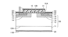
- FIG. 1 is a cross sectional view schematically showing a configuration of a semiconductor device in an embodiment of the present invention. It is a flowchart which shows the outline of the manufacturing method of the semiconductor device of FIG. It is a flowchart which shows the detail of the ohmic electrode formation process in FIG.
- FIG. 7 is a cross sectional view schematically showing a first step of a method of manufacturing the semiconductor device of FIG. 1.
- FIG. 7 is a cross sectional view schematically showing a second step of the method for manufacturing the semiconductor device of FIG. 1.
- FIG. 14 is a cross sectional view schematically showing a third step of the method for manufacturing the semiconductor device of FIG. 1.
- FIG. 14 is a cross sectional view schematically showing a fourth step of the method for manufacturing the semiconductor device of FIG. 1.
- FIG. 14 is a cross sectional view schematically showing a fifth step of the method for manufacturing the semiconductor device of FIG. 1.
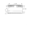
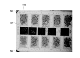
- FIG. 14 is a cross sectional view schematically showing a sixth step of the method for manufacturing the semiconductor device of FIG. 1. It is an optical microscope photograph which shows the mode of the thermal diffusion of Al atom at the time of annealing Ti / Al pattern embedded in the silicon dioxide film. It is an optical microscope photograph which shows the mode of the thermal diffusion of Al atom at the time of annealing Al pattern embedded in the silicon dioxide film.
- MOSFET Metal Oxide Semiconductor Field Effect Transistor
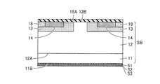
- MOSFET 1 has a silicon carbide substrate SB, a gate insulating film 15, a gate electrode 17, a source electrode 22, a passivation film 21, and a drain electrode 20.
- Source electrode 22 has contact electrode 16 and source interconnection 19.
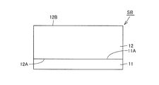
- Silicon carbide substrate SB has a substrate surface 12B.
- a gate insulating film 15 is provided to cover a part of the substrate surface 12B.
- the gate electrode 17 covers a part of the gate insulating film 15.
- the contact electrode 16 is provided on the substrate surface 12 B so as to be in contact with and adjacent to the gate insulating film 15.
- the contact electrode 16 also contains an alloy having Al atoms. Al atoms are not diffused from the contact electrode 16 to a portion of the gate insulating film 15 sandwiched by the substrate surface 12 B and the gate electrode 17.
- an alloy having an Al atom described above for example, an alloy of Al and at least one of Ti, Ni, and Si can be used.
- the gate insulating film 15 for example, a SiO 2 film, a SiON film, or an ONO film can be used.
- the ONO film is a film having a three-layer structure of oxide film-nitride film-oxide film. SiO 2 can be used as this oxide film, and Si 3 N 4 can be used as this nitride film.
- MOSFET 1 is made of silicon carbide (SiC), n + SiC wafer 11 which is a wafer of n type conductivity (first conductivity type), and SiC is a semiconductor of n conductivity type (first conductivity type) N - SiC layer 12 as a layer, a pair of p bodies 13 as a second conductivity type region of p type conductivity (second conductivity type), and high concentration of n type conductivity (first conductivity type)
- An n + source region 14 as a first conductivity type region and ap + region 18 as a high concentration second conductivity type region of p type (second conductivity type) as a conductivity type are provided.
- the n ⁇ SiC layer 12 in which the p body 13, the n + source region 14 and the p + region 18 are formed, and the n + SiC wafer 11 constitute a silicon carbide substrate SB made of silicon carbide.
- the n + SiC wafer 11 contains a high concentration n-type impurity (an impurity whose conductivity type is n-type), for example, N (nitrogen).
- the n ⁇ SiC layer 12 is formed on one main surface 11 A of the n + SiC wafer 11 to a thickness of, for example, about 10 ⁇ m, and includes an n-type impurity to have an n-type conductivity type.
- the n-type impurity contained in n - SiC layer 12 is, for example, N (nitrogen), and is contained at a concentration lower than that of the n-type impurity contained in n + SiC wafer 11, for example, 5 ⁇ 10 15 cm -3 ing.
- the pair of p bodies 13 are formed separately from each other so as to include the substrate surface 12B in the n - SiC layer 12, and by including p type impurities (impurity of the conductivity type is p type), the conductivity type is p type (2nd conductivity type).
- the p-type impurity contained in p body 13 is, for example, Al, B (boron) or the like, and is contained at a concentration lower than that of the n-type impurity contained in n + SiC wafer 11, for example, 1 ⁇ 10 17 cm -3. It is done.
- the n + source region 14 is formed in each of the pair of p bodies 13 so as to include the substrate surface 12 B and be surrounded by the p bodies 13.
- the n + source region 14 contains an n-type impurity such as P (phosphorus) at a concentration higher than that of the n-type impurity contained in the n ⁇ SiC layer 12, for example, 1 ⁇ 10 20 cm ⁇ 3 .
- the p + region 18 when viewed from n + source region 14 formed in the interior of one of the p body 13 of the pair of p bodies 13, the n + source region 14 formed within the other p body 13 Is formed to include the substrate surface 12B on the opposite side.
- the p + region 18 contains a p-type impurity such as Al or B at a concentration higher than that of the p-type impurity contained in the p body 13, for example, 1 ⁇ 10 20 cm ⁇ 3 .
- the MOSFET 1 further includes a gate insulating film 15, a gate electrode 17, a pair of contact electrodes 16, a source wiring 19, a drain electrode 20, and a passivation film 21.
- Gate insulating film 15 is in contact with substrate surface 12 B, and substrate surface 12 B of n ⁇ SiC layer 12 so as to extend from the upper surface of one n + source region 14 to the upper surface of the other n + source region 14. It is formed on top.
- the gate insulating film 15 contains silicon oxide, and the silicon oxide contains silicon dioxide (SiO 2 ). That is, gate insulating film 15 is, for example, a silicon dioxide film.
- Gate electrode 17 is arranged in contact with gate insulating film 15 so as to extend from above one n + source region 14 to above the other n + source region 14.
- the gate electrode 17 is made of a conductor such as polysilicon or Al.
- the contact electrodes 16 extend from above each of the pair of n + source regions 14 to above the p + regions 18 in a direction away from the gate insulating film 15 and are disposed in contact with the substrate surface 12B.
- the contact electrode 16 is composed of a titanium (Ti) atom, an aluminum (Al) atom, a silicon (Si) atom, a carbon (C) atom, and the balance inevitable impurities.
- the unavoidable impurities include oxygen (O) atoms which are inevitably mixed in the manufacturing process.
- the contact electrode 16 has aluminum atoms and titanium atoms in a region including the interface with the n ⁇ SiC layer 12 in which the source region 14 and the p + region 18 are formed.
- the source wiring 19 is formed in contact with the contact electrode 16 and made of a conductor such as Al.
- Source interconnection 19 is electrically connected to n + source region 14 via contact electrode 16.
- Source interconnection 19 and contact electrode 16 constitute source electrode 22.
- the drain electrode 20 is formed in contact with the other main surface 11B which is the main surface opposite to the one main surface 11A which is the main surface on which the n - SiC layer 12 is formed in the n + SiC wafer 11 It is done.
- the drain electrode 20 may have, for example, the same configuration as that of the contact electrode 16 described above, or may be made of another material such as Ni, which can make ohmic contact with the n + SiC wafer 11. Thus, the drain electrode 20 is electrically connected to the n + SiC wafer 11.
- the passivation film 21 is formed to extend from above the one source wiring 19 to above the gate electrode 17 and onto the other source wiring 19.
- Passivation film 21 is made of, for example, SiO 2 and has functions of electrically insulating source interconnection 19 and gate electrode 17 from the outside and protecting MOSFET 1.
- a reverse bias is applied between p body 13 and n - SiC layer 12 located immediately below gate insulating film 15. .
- a positive voltage is applied to gate electrode 17
- an inversion layer is formed in channel region 13A in the vicinity of contact with gate insulating film 15 of p body 13.
- the n + source region 14 and the n ⁇ SiC layer 12 are electrically connected, and a current flows between the source electrode 22 and the drain electrode 20.
- a substrate preparation process is performed as a process (S10).
- a first conductivity type SiC wafer is prepared.
- n + SiC wafer 11 is prepared, which is made of, for example, hexagonal SiC and contains n-type impurities and whose conductivity type is n-type.
- an n-type layer forming step is performed as a step (S20).
- a semiconductor layer of the first conductivity type is formed on n + SiC wafer 11.
- n ⁇ SiC layer 12 is formed on one main surface 11 A of n + SiC wafer 11 by epitaxial growth.
- the epitaxial growth can be performed, for example, using a mixed gas of SiH 4 (silane) and C 3 H 8 (propane) as a source gas.
- N is introduced as an n-type impurity.
- n including n-type impurity of lower concentration than the n-type impurity contained in n + SiC wafer 11 - it is possible to form a SiC layer 12.
- a p body forming step is performed as a step (S30).
- a second conductivity type region of the second conductivity type is formed to include substrate surface 12B in n - SiC layer 12.
- an oxide film made of SiO 2 is formed on substrate surface 12B, for example, by CVD (Chemical Vapor Deposition).
- CVD Chemical Vapor Deposition
- exposure and development are performed to form a resist film having an opening in a region corresponding to the shape of the p body 13 as a desired second conductivity type region.
- the oxide film is partially removed by, for example, RIE (Reactive Ion Etching), whereby an oxide film having an opening pattern on n ⁇ SiC layer 12 is obtained.
- Mask layer is formed.
- the p-type impurity such as Al n - by implanting ions into the SiC layer 12, n - p body 13 in the SiC layer 12 is formed Be done.
- an n + region forming step is performed as a step (S40).
- a high concentration first conductivity type region including an impurity of the first conductivity type higher in concentration than n - SiC layer 12 is formed in the region including substrate surface 12B in p body 13.
- the desired n + source region is performed in the same procedure as step (S30).
- a mask layer having an opening in a region corresponding to the shape of 14 is formed.
- an n + source region 14 is formed by introducing an n type impurity such as P into the n ⁇ SiC layer 12 by ion implantation.
- ap + region forming step is performed as a step (S50).
- this step (S50) referring to FIG. 5, it is formed in the inside of the other p body 13 as seen from n + source region 14 formed in one p body 13 of the pair of p bodies 13
- the high concentration second conductivity type region (p + region 18) is formed on the opposite side of the n + source region 14 so as to include the substrate surface 12B. Specifically, referring to FIG.
- a mask layer having an opening in a region corresponding to the desired shape of p + region 18 is formed in the same procedure as steps (S30) and (S40), and this is used as a mask
- the p + region 18 is formed by introducing p type impurities such as Al and B into the n ⁇ SiC layer 12 by ion implantation.
- an activation annealing step is performed as a step (S60).
- the n - SiC layer 12 subjected to the ion implantation is heated to about 1700 ° C. in an Ar (argon) atmosphere, for example, and held for about 30 minutes to introduce the ion implantation.
- Activation annealing which is a heat treatment to activate the impurities, is performed.
- a gate insulating film forming step is performed as a step (S70).
- steps (S10) to (S60) are performed to heat n + SiC wafer 11 in which n - SiC layer 12 including the desired ion implantation region is formed. It is oxidized. Thermal oxidation can be performed, for example, by heating to about 1300 ° C. in an oxygen atmosphere and holding for about 40 minutes.
- silicon dioxide gate insulating film 15 see FIG. 1 and the thermal oxide film 15A (for example, about the thickness 50 nm) should be made of (SiO 2) is formed on the substrate surface 12B.
- a drain electrode forming step is performed as a step (S80).
- step (S80) referring to FIG. 6, Ti film 51 made of Ti, Al film 52 made of Al, and Si film 53 made of Si are formed in this order on main surface 11B of n + SiC wafer 11. Be done.
- an alloying step of this laminated film is carried out. Specifically, it is heated to a temperature of 550 ° C. to 1200 ° C., preferably 900 ° C. to 1100 ° C., for example 1000 ° C. in an inert gas atmosphere such as Ar, for a time of 10 minutes or less, eg 2 A heat treatment is performed that is held for a minute.
- the drain electrode 20 is formed.
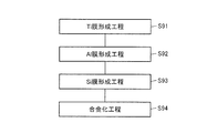
- step (S90) an ohmic electrode forming step is performed as a step (S90).
- step (S90) referring to FIG. 3, first, a Ti film forming step, an Al film forming step and a Si film forming step are performed in this order as steps (S91) to (S93).
- thermal oxide film 15A first, after a resist is applied on thermal oxide film 15A, exposure and development are performed to correspond to the region where contact electrode 16 (see FIG. 1) is to be formed. A resist film 91 having an opening 91A is formed. Then, using the resist film 91 as a mask, the thermal oxide film 15A is partially removed by RIE, for example, to form a gate insulating film 15 which covers a part of the substrate surface 12B. Thereafter, a Ti film 51 of Ti, an Al film 52 of Al, and a Si film 53 of Si are formed in this order by sputtering, for example, on the substrate surface 12B.
- a contact electrode 16m to be a contact electrode 16 (FIG. 1) later is formed on the substrate surface 12B so as to be adjacent to and in contact with the gate insulating film 15.
- a Ti film 51 having a thickness of 100 ⁇ to 400 ⁇ is preferably formed. Thereby, an ohmic contact electrode with low resistance can be stably formed.
- the step (S92) it is preferable to form an Al film 52 having a thickness not less than 1.5 times and not more than 6 times the thickness of the Ti film 51 formed in the step (S91). As a result, it is possible to manufacture the contact electrode 16 in which the contact resistance with the n + source region 14 and the p body 13 is more reliably reduced.
- the Si film 53 having a thickness of 100 ⁇ or more and 500 ⁇ or less. Thereby, an ohmic contact electrode with low resistance can be stably formed.
- an alloying step is performed as a step (S94). Specifically, referring to FIGS. 8 and 9, contact electrode 16m is annealed by laser light in an inert gas atmosphere such as Ar. As a result, Ti, Al, Si contained in the Ti film 51, the Al film 52 and the Si film 53, and Si and C contained in the n - SiC layer 12 are alloyed. As a result, as shown in FIG. 9, while extending from above each of the pair of n + source regions 14 to above p + region 18 in a direction away from gate insulating film 15, it is disposed in contact with substrate surface 12B. Contact electrodes 16 are formed.
- the annealing by laser light is performed by local heating in a very short time, the diffusion distance of atoms during the annealing is reduced. Therefore, Al atoms are not diffused from the contact electrode 16m to a portion of the gate insulating film 15 which is to be sandwiched by the substrate surface 12B and the gate electrode 17 (FIG. 1) later.
- the n + SiC wafer 11 is preferably heated in a mixed gas of an inert gas, in particular, Ar and / or N 2 , and hydrogen.
- an inert gas in particular, Ar and / or N 2 , and hydrogen.
- a gate electrode formation step is performed as a step (S100).
- step (S100) referring to FIG. 1 again, gate electrode 17 covering a part of gate insulating film 15 is formed. The end of the gate electrode 17 is disposed away from the end of the gate insulating film 15.
- polysilicon for example, a conductor, so that the gate electrode 17 made of Al is, extends from the top one n + source region 14 to above the other n + source region 14, a gate insulating film Formed directly on 15
- the polysilicon can be contained at a high concentration of P exceeding 1 ⁇ 10 20 cm ⁇ 3 .
- a source wiring formation step is performed as a step (S110).
- source interconnection 19 made of Al, which is a conductor, is formed on the upper surface of contact electrode 16 by evaporation, for example.
- Source electrode 22 (see FIG. 1) is completed by the above-described step (S90) and this step (S110).
- a passivation film formation step is performed as a step (S120).
- this passivation film made of, for example, SiO 2 so as to extend from above one source interconnection 19 to above gate electrode 17 and onto the other source interconnection 19. 21 are formed.
- Passivation film 21 can be formed, for example, by the CVD method.
- MOSFET 1 (see FIG. 1) is completed by the above steps (S10) to (S120).
- MOSFET 1 of the present embodiment Al atoms are not diffused from contact electrode 16 in the portion of gate insulating film 15 sandwiched by substrate surface 12 B and gate electrode 17. Therefore, the reliability of the electrical insulation between gate electrode 17 and silicon carbide substrate SB is enhanced.
- annealing of contact electrode 16m is performed by laser light, so that annealing is performed by local heating in a short time as compared with the case where other annealing methods are used. . Therefore, the diffusion distance of the Al atoms of the contact electrode 16m into the gate insulating film 15 is suppressed, so that the Al atoms do not reach the portion of the gate insulating film 15 sandwiched by the substrate surface and the gate electrode 17. Can. Thereby, the reliability of the electrical insulation between gate electrode 17 and silicon carbide substrate SB is enhanced.
- the wavelength of the laser light is 386 nm or less.
- laser light by the third harmonic of a YAG laser is used.
- the laser light has photon energy equal to or higher than the energy corresponding to the band gap of polytype 4H silicon carbide.
- the absorption of the laser light occurs more reliably on the surface of silicon carbide substrate SB, and therefore, the annealing can be performed more efficiently.
- the pulse width of the laser beam is 10 ⁇ s or less, more preferably 100 ns or less. Thereby, annealing is performed in a shorter time. Therefore, the diffusion of Al atoms can be suppressed more reliably.
- the energy density of the addition the laser beam per pulse is preferably 0.3 J / cm 2 or more 1.5 J / cm 2 or less, and more preferably, 0.5 J / cm 2 or more 1.3 J / cm 2 or less.
- the region where Al atoms are not diffused in the gate insulating film 15 is a region where Al atoms are not substantially diffused, in other words, the gate insulating film 15 is a contact electrode 16. It is a region that is not substantially subjected to the diffusion of Al atoms from.
- the demarcation of the boundary between the region where Al atoms are not substantially diffused and the region where the atoms are substantially diffused can be performed, for example, by observation with an optical microscope. This observation example using a test pattern will be described below.
- the thermal diffusion of Al atoms when the Ti / Al pattern 101 embedded in the silicon dioxide film was annealed was observed by an optical microscope.
- the silicon dioxide film and the Ti / Al pattern 101 correspond to the gate insulating film 15 and the contact electrode 16 described above. According to this observation, it was possible to divide the silicon dioxide film into the first region DF and the second region ND due to the remarkable difference in lightness.
- the Al concentration of each of the first region DF and the second region is measured by the composition analysis method, the first region DF has a high Al concentration value, and the second region ND is remarkable compared to the first region DF It was found that Al had a small Al concentration value, and Al atoms were not substantially diffused into the second region ND.
- the compositional analysis method energy dispersive X-ray diffraction, Auger electron spectroscopy, and secondary ion mass spectrometry were used.
- the state of thermal diffusion of Al atoms when the Al pattern 102 embedded in the silicon dioxide film was annealed was observed by an optical microscope.
- Each of the silicon dioxide film and the Al pattern 102 corresponds to the gate insulating film 15 and the contact electrode 16 described above. Also in this observation, the silicon dioxide film could be divided into the first region DF and the second region ND due to the remarkable difference in lightness.
- the spread of the first region DF is smaller in the first example. From this, it is understood that the diffusion distance of Al atoms into the silicon dioxide film is shorter from the Ti / Al pattern 101 than that from the Al pattern 102. Therefore, if Ti / Al is used as the material of the contact electrode 16, the diffusion distance of Al atoms from the contact electrode 16 into the gate insulating film 15 can be suppressed as compared with the case of using Al. I found that.
Landscapes
- Engineering & Computer Science (AREA)
- Physics & Mathematics (AREA)
- Microelectronics & Electronic Packaging (AREA)
- Power Engineering (AREA)
- Condensed Matter Physics & Semiconductors (AREA)
- General Physics & Mathematics (AREA)
- Manufacturing & Machinery (AREA)
- Computer Hardware Design (AREA)
- Chemical & Material Sciences (AREA)
- Crystallography & Structural Chemistry (AREA)
- High Energy & Nuclear Physics (AREA)
- Electromagnetism (AREA)
- Optics & Photonics (AREA)
- Health & Medical Sciences (AREA)
- Toxicology (AREA)
- Electrodes Of Semiconductors (AREA)
Priority Applications (5)
| Application Number | Priority Date | Filing Date | Title |
|---|---|---|---|
| KR1020127026283A KR20130122514A (ko) | 2010-11-01 | 2011-10-19 | 반도체 장치 및 그 제조 방법 |
| US13/581,980 US8691679B2 (en) | 2010-11-01 | 2011-10-19 | Semiconductor device and method of manufacturing the same |
| CA2791183A CA2791183A1 (en) | 2010-11-01 | 2011-10-19 | Semiconductor device and method of manufacturing the same |
| EP11837874.4A EP2637213A4 (en) | 2010-11-01 | 2011-10-19 | SEMICONDUCTOR COMPONENT AND MANUFACTURING METHOD THEREFOR |
| CN201180018726.2A CN102844871B (zh) | 2010-11-01 | 2011-10-19 | 半导体装置及其制造方法 |
Applications Claiming Priority (2)
| Application Number | Priority Date | Filing Date | Title |
|---|---|---|---|
| JP2010-245150 | 2010-11-01 | ||
| JP2010245150A JP5668414B2 (ja) | 2010-11-01 | 2010-11-01 | 半導体装置の製造方法 |
Publications (1)
| Publication Number | Publication Date |
|---|---|
| WO2012060223A1 true WO2012060223A1 (ja) | 2012-05-10 |
Family
ID=46024340
Family Applications (1)
| Application Number | Title | Priority Date | Filing Date |
|---|---|---|---|
| PCT/JP2011/073996 WO2012060223A1 (ja) | 2010-11-01 | 2011-10-19 | 半導体装置およびその製造方法 |
Country Status (8)
Families Citing this family (11)
| Publication number | Priority date | Publication date | Assignee | Title |
|---|---|---|---|---|
| JP2014003253A (ja) * | 2012-06-21 | 2014-01-09 | Sumitomo Electric Ind Ltd | 炭化珪素半導体装置 |
| JP5875684B2 (ja) * | 2012-07-09 | 2016-03-02 | 株式会社日立製作所 | Mos型電界効果トランジスタ |
| JP2014063948A (ja) * | 2012-09-24 | 2014-04-10 | Sumitomo Electric Ind Ltd | 炭化珪素半導体装置の製造方法 |
| JP2014078659A (ja) * | 2012-10-12 | 2014-05-01 | Sumitomo Electric Ind Ltd | 半導体装置の製造方法 |
| WO2014065018A1 (ja) | 2012-10-23 | 2014-05-01 | 富士電機株式会社 | 半導体装置の製造方法 |
| EP2763159A1 (en) * | 2013-01-30 | 2014-08-06 | University College Cork | Improved low resistance contacts for semiconductor devices |
| JP6037083B2 (ja) | 2014-04-18 | 2016-11-30 | 富士電機株式会社 | 半導体装置の製造方法 |
| CN105518829B (zh) * | 2014-04-18 | 2018-01-26 | 富士电机株式会社 | 半导体装置的制造方法 |
| DE112014003658T5 (de) * | 2014-04-18 | 2016-05-12 | Fuji Electric Co., Ltd. | Verfahren zum Herstellen einer Halbleitervorrichtung |
| JP2016046311A (ja) * | 2014-08-20 | 2016-04-04 | 住友電気工業株式会社 | 炭化珪素半導体装置 |
| JP6387791B2 (ja) | 2014-10-29 | 2018-09-12 | 富士電機株式会社 | 半導体装置の製造方法 |
Citations (4)
| Publication number | Priority date | Publication date | Assignee | Title |
|---|---|---|---|---|
| JPH10284436A (ja) * | 1997-04-11 | 1998-10-23 | Matsushita Electric Ind Co Ltd | オーミック電極形成方法 |
| JP2004158702A (ja) * | 2002-11-07 | 2004-06-03 | C Tekku:Kk | 半導体装置製造方法 |
| WO2009128419A1 (ja) | 2008-04-15 | 2009-10-22 | 住友電気工業株式会社 | 半導体装置 |
| JP2010087397A (ja) * | 2008-10-02 | 2010-04-15 | Sumitomo Electric Ind Ltd | 炭化珪素半導体装置 |
Family Cites Families (6)
| Publication number | Priority date | Publication date | Assignee | Title |
|---|---|---|---|---|
| CN1131548C (zh) | 1997-04-04 | 2003-12-17 | 松下电器产业株式会社 | 半导体装置 |
| US6599644B1 (en) * | 2000-10-06 | 2003-07-29 | Foundation For Research & Technology-Hellas | Method of making an ohmic contact to p-type silicon carbide, comprising titanium carbide and nickel silicide |
| CN100483631C (zh) * | 2003-08-14 | 2009-04-29 | 克里公司 | 金属-碳化硅欧姆接触的局部退火及其形成的装置 |
| US20050104072A1 (en) * | 2003-08-14 | 2005-05-19 | Slater David B.Jr. | Localized annealing of metal-silicon carbide ohmic contacts and devices so formed |
| US8866150B2 (en) * | 2007-05-31 | 2014-10-21 | Cree, Inc. | Silicon carbide power devices including P-type epitaxial layers and direct ohmic contacts |
| US8188538B2 (en) * | 2008-12-25 | 2012-05-29 | Rohm Co., Ltd. | Semiconductor device and method of manufacturing semiconductor device |
-
2010
- 2010-11-01 JP JP2010245150A patent/JP5668414B2/ja active Active
-
2011
- 2011-10-19 WO PCT/JP2011/073996 patent/WO2012060223A1/ja active Application Filing
- 2011-10-19 KR KR1020127026283A patent/KR20130122514A/ko not_active Withdrawn
- 2011-10-19 CN CN201180018726.2A patent/CN102844871B/zh active Active
- 2011-10-19 CA CA2791183A patent/CA2791183A1/en not_active Abandoned
- 2011-10-19 EP EP11837874.4A patent/EP2637213A4/en not_active Ceased
- 2011-10-19 US US13/581,980 patent/US8691679B2/en active Active
- 2011-10-25 TW TW100138735A patent/TW201222820A/zh unknown
Patent Citations (4)
| Publication number | Priority date | Publication date | Assignee | Title |
|---|---|---|---|---|
| JPH10284436A (ja) * | 1997-04-11 | 1998-10-23 | Matsushita Electric Ind Co Ltd | オーミック電極形成方法 |
| JP2004158702A (ja) * | 2002-11-07 | 2004-06-03 | C Tekku:Kk | 半導体装置製造方法 |
| WO2009128419A1 (ja) | 2008-04-15 | 2009-10-22 | 住友電気工業株式会社 | 半導体装置 |
| JP2010087397A (ja) * | 2008-10-02 | 2010-04-15 | Sumitomo Electric Ind Ltd | 炭化珪素半導体装置 |
Non-Patent Citations (1)
| Title |
|---|
| See also references of EP2637213A4 |
Also Published As
| Publication number | Publication date |
|---|---|
| US8691679B2 (en) | 2014-04-08 |
| TW201222820A (en) | 2012-06-01 |
| EP2637213A1 (en) | 2013-09-11 |
| CN102844871A (zh) | 2012-12-26 |
| CN102844871B (zh) | 2015-05-13 |
| US20120326167A1 (en) | 2012-12-27 |
| EP2637213A4 (en) | 2014-06-25 |
| KR20130122514A (ko) | 2013-11-07 |
| CA2791183A1 (en) | 2012-05-10 |
| JP2012099599A (ja) | 2012-05-24 |
| JP5668414B2 (ja) | 2015-02-12 |
Similar Documents
| Publication | Publication Date | Title |
|---|---|---|
| JP5668414B2 (ja) | 半導体装置の製造方法 | |
| JP5525940B2 (ja) | 半導体装置および半導体装置の製造方法 | |
| JP4539684B2 (ja) | 炭化珪素半導体装置およびその製造方法 | |
| KR101442886B1 (ko) | 반도체 장치 및 그 제조 방법 | |
| JP6164220B2 (ja) | 半導体装置の製造方法 | |
| TW201624698A (zh) | 半導體裝置及其製造方法 | |
| JP2011060901A (ja) | 半導体装置および半導体装置の製造方法 | |
| US8847237B2 (en) | Silicon carbide semiconductor device and method for manufacturing same | |
| US8729567B2 (en) | Silicon carbide semiconductor device | |
| JP6729824B1 (ja) | 炭化珪素半導体装置および炭化珪素半導体装置の製造方法 | |
| US8716129B2 (en) | Method for manufacturing silicon carbide semiconductor device | |
| JP7532965B2 (ja) | 炭化珪素半導体装置および炭化珪素半導体装置の製造方法 | |
| US8866156B2 (en) | Silicon carbide semiconductor device and method for manufacturing same | |
| JP7669310B2 (ja) | 半導体装置の製造方法、半導体装置、インバータ回路、駆動装置、車両、及び、昇降機 | |
| JP5991629B2 (ja) | 半導体装置および半導体装置の製造方法 | |
| JP5439856B2 (ja) | 絶縁ゲート型電界効果トランジスタ | |
| JP2022187367A (ja) | 炭化珪素半導体装置の製造方法および炭化珪素半導体装置 |
Legal Events
| Date | Code | Title | Description |
|---|---|---|---|
| WWE | Wipo information: entry into national phase |
Ref document number: 201180018726.2 Country of ref document: CN |
|
| 121 | Ep: the epo has been informed by wipo that ep was designated in this application |
Ref document number: 11837874 Country of ref document: EP Kind code of ref document: A1 |
|
| ENP | Entry into the national phase |
Ref document number: 2791183 Country of ref document: CA |
|
| WWE | Wipo information: entry into national phase |
Ref document number: 2011837874 Country of ref document: EP |
|
| WWE | Wipo information: entry into national phase |
Ref document number: 13581980 Country of ref document: US |
|
| ENP | Entry into the national phase |
Ref document number: 20127026283 Country of ref document: KR Kind code of ref document: A |
|
| NENP | Non-entry into the national phase |
Ref country code: DE |