WO2012029671A1 - 半導体装置、半導体装置ユニット、アクティブマトリクス基板、液晶パネル、および液晶表示装置 - Google Patents
半導体装置、半導体装置ユニット、アクティブマトリクス基板、液晶パネル、および液晶表示装置 Download PDFInfo
- Publication number
- WO2012029671A1 WO2012029671A1 PCT/JP2011/069346 JP2011069346W WO2012029671A1 WO 2012029671 A1 WO2012029671 A1 WO 2012029671A1 JP 2011069346 W JP2011069346 W JP 2011069346W WO 2012029671 A1 WO2012029671 A1 WO 2012029671A1
- Authority
- WO
- WIPO (PCT)
- Prior art keywords
- transistor
- semiconductor device
- wiring
- electrode
- capacitor
- Prior art date
- Legal status (The legal status is an assumption and is not a legal conclusion. Google has not performed a legal analysis and makes no representation as to the accuracy of the status listed.)
- Ceased
Links
Images



Classifications
-
- G—PHYSICS
- G09—EDUCATION; CRYPTOGRAPHY; DISPLAY; ADVERTISING; SEALS
- G09G—ARRANGEMENTS OR CIRCUITS FOR CONTROL OF INDICATING DEVICES USING STATIC MEANS TO PRESENT VARIABLE INFORMATION
- G09G3/00—Control arrangements or circuits, of interest only in connection with visual indicators other than cathode-ray tubes
- G09G3/20—Control arrangements or circuits, of interest only in connection with visual indicators other than cathode-ray tubes for presentation of an assembly of a number of characters, e.g. a page, by composing the assembly by combination of individual elements arranged in a matrix no fixed position being assigned to or needed to be assigned to the individual characters or partial characters
- G09G3/34—Control arrangements or circuits, of interest only in connection with visual indicators other than cathode-ray tubes for presentation of an assembly of a number of characters, e.g. a page, by composing the assembly by combination of individual elements arranged in a matrix no fixed position being assigned to or needed to be assigned to the individual characters or partial characters by control of light from an independent source
- G09G3/36—Control arrangements or circuits, of interest only in connection with visual indicators other than cathode-ray tubes for presentation of an assembly of a number of characters, e.g. a page, by composing the assembly by combination of individual elements arranged in a matrix no fixed position being assigned to or needed to be assigned to the individual characters or partial characters by control of light from an independent source using liquid crystals
- G09G3/3611—Control of matrices with row and column drivers
- G09G3/3648—Control of matrices with row and column drivers using an active matrix
-
- H—ELECTRICITY
- H10—SEMICONDUCTOR DEVICES; ELECTRIC SOLID-STATE DEVICES NOT OTHERWISE PROVIDED FOR
- H10D—INORGANIC ELECTRIC SEMICONDUCTOR DEVICES
- H10D1/00—Resistors, capacitors or inductors
- H10D1/60—Capacitors
- H10D1/68—Capacitors having no potential barriers
-
- G—PHYSICS
- G09—EDUCATION; CRYPTOGRAPHY; DISPLAY; ADVERTISING; SEALS
- G09G—ARRANGEMENTS OR CIRCUITS FOR CONTROL OF INDICATING DEVICES USING STATIC MEANS TO PRESENT VARIABLE INFORMATION
- G09G3/00—Control arrangements or circuits, of interest only in connection with visual indicators other than cathode-ray tubes
- G09G3/20—Control arrangements or circuits, of interest only in connection with visual indicators other than cathode-ray tubes for presentation of an assembly of a number of characters, e.g. a page, by composing the assembly by combination of individual elements arranged in a matrix no fixed position being assigned to or needed to be assigned to the individual characters or partial characters
- G09G3/34—Control arrangements or circuits, of interest only in connection with visual indicators other than cathode-ray tubes for presentation of an assembly of a number of characters, e.g. a page, by composing the assembly by combination of individual elements arranged in a matrix no fixed position being assigned to or needed to be assigned to the individual characters or partial characters by control of light from an independent source
- G09G3/36—Control arrangements or circuits, of interest only in connection with visual indicators other than cathode-ray tubes for presentation of an assembly of a number of characters, e.g. a page, by composing the assembly by combination of individual elements arranged in a matrix no fixed position being assigned to or needed to be assigned to the individual characters or partial characters by control of light from an independent source using liquid crystals
- G09G3/3611—Control of matrices with row and column drivers
-
- H—ELECTRICITY
- H10—SEMICONDUCTOR DEVICES; ELECTRIC SOLID-STATE DEVICES NOT OTHERWISE PROVIDED FOR
- H10D—INORGANIC ELECTRIC SEMICONDUCTOR DEVICES
- H10D84/00—Integrated devices formed in or on semiconductor substrates that comprise only semiconducting layers, e.g. on Si wafers or on GaAs-on-Si wafers
-
- H—ELECTRICITY
- H10—SEMICONDUCTOR DEVICES; ELECTRIC SOLID-STATE DEVICES NOT OTHERWISE PROVIDED FOR
- H10D—INORGANIC ELECTRIC SEMICONDUCTOR DEVICES
- H10D86/00—Integrated devices formed in or on insulating or conducting substrates, e.g. formed in silicon-on-insulator [SOI] substrates or on stainless steel or glass substrates
- H10D86/40—Integrated devices formed in or on insulating or conducting substrates, e.g. formed in silicon-on-insulator [SOI] substrates or on stainless steel or glass substrates characterised by multiple TFTs
- H10D86/481—Integrated devices formed in or on insulating or conducting substrates, e.g. formed in silicon-on-insulator [SOI] substrates or on stainless steel or glass substrates characterised by multiple TFTs integrated with passive devices, e.g. auxiliary capacitors
-
- H—ELECTRICITY
- H10—SEMICONDUCTOR DEVICES; ELECTRIC SOLID-STATE DEVICES NOT OTHERWISE PROVIDED FOR
- H10D—INORGANIC ELECTRIC SEMICONDUCTOR DEVICES
- H10D86/00—Integrated devices formed in or on insulating or conducting substrates, e.g. formed in silicon-on-insulator [SOI] substrates or on stainless steel or glass substrates
- H10D86/40—Integrated devices formed in or on insulating or conducting substrates, e.g. formed in silicon-on-insulator [SOI] substrates or on stainless steel or glass substrates characterised by multiple TFTs
- H10D86/60—Integrated devices formed in or on insulating or conducting substrates, e.g. formed in silicon-on-insulator [SOI] substrates or on stainless steel or glass substrates characterised by multiple TFTs wherein the TFTs are in active matrices
-
- H—ELECTRICITY
- H10—SEMICONDUCTOR DEVICES; ELECTRIC SOLID-STATE DEVICES NOT OTHERWISE PROVIDED FOR
- H10H—INORGANIC LIGHT-EMITTING SEMICONDUCTOR DEVICES HAVING POTENTIAL BARRIERS
- H10H20/00—Individual inorganic light-emitting semiconductor devices having potential barriers, e.g. light-emitting diodes [LED]
- H10H20/80—Constructional details
- H10H20/81—Bodies
- H10H20/813—Bodies having a plurality of light-emitting regions, e.g. multi-junction LEDs or light-emitting devices having photoluminescent regions within the bodies
-
- G—PHYSICS
- G02—OPTICS
- G02F—OPTICAL DEVICES OR ARRANGEMENTS FOR THE CONTROL OF LIGHT BY MODIFICATION OF THE OPTICAL PROPERTIES OF THE MEDIA OF THE ELEMENTS INVOLVED THEREIN; NON-LINEAR OPTICS; FREQUENCY-CHANGING OF LIGHT; OPTICAL LOGIC ELEMENTS; OPTICAL ANALOGUE/DIGITAL CONVERTERS
- G02F1/00—Devices or arrangements for the control of the intensity, colour, phase, polarisation or direction of light arriving from an independent light source, e.g. switching, gating or modulating; Non-linear optics
- G02F1/01—Devices or arrangements for the control of the intensity, colour, phase, polarisation or direction of light arriving from an independent light source, e.g. switching, gating or modulating; Non-linear optics for the control of the intensity, phase, polarisation or colour
- G02F1/13—Devices or arrangements for the control of the intensity, colour, phase, polarisation or direction of light arriving from an independent light source, e.g. switching, gating or modulating; Non-linear optics for the control of the intensity, phase, polarisation or colour based on liquid crystals, e.g. single liquid crystal display cells
- G02F1/133—Constructional arrangements; Operation of liquid crystal cells; Circuit arrangements
- G02F1/1333—Constructional arrangements; Manufacturing methods
- G02F1/1345—Conductors connecting electrodes to cell terminals
- G02F1/13454—Drivers integrated on the active matrix substrate
-
- G—PHYSICS
- G02—OPTICS
- G02F—OPTICAL DEVICES OR ARRANGEMENTS FOR THE CONTROL OF LIGHT BY MODIFICATION OF THE OPTICAL PROPERTIES OF THE MEDIA OF THE ELEMENTS INVOLVED THEREIN; NON-LINEAR OPTICS; FREQUENCY-CHANGING OF LIGHT; OPTICAL LOGIC ELEMENTS; OPTICAL ANALOGUE/DIGITAL CONVERTERS
- G02F1/00—Devices or arrangements for the control of the intensity, colour, phase, polarisation or direction of light arriving from an independent light source, e.g. switching, gating or modulating; Non-linear optics
- G02F1/01—Devices or arrangements for the control of the intensity, colour, phase, polarisation or direction of light arriving from an independent light source, e.g. switching, gating or modulating; Non-linear optics for the control of the intensity, phase, polarisation or colour
- G02F1/13—Devices or arrangements for the control of the intensity, colour, phase, polarisation or direction of light arriving from an independent light source, e.g. switching, gating or modulating; Non-linear optics for the control of the intensity, phase, polarisation or colour based on liquid crystals, e.g. single liquid crystal display cells
- G02F1/133—Constructional arrangements; Operation of liquid crystal cells; Circuit arrangements
- G02F1/136—Liquid crystal cells structurally associated with a semi-conducting layer or substrate, e.g. cells forming part of an integrated circuit
- G02F1/1362—Active matrix addressed cells
- G02F1/136277—Active matrix addressed cells formed on a semiconductor substrate, e.g. of silicon
-
- G—PHYSICS
- G09—EDUCATION; CRYPTOGRAPHY; DISPLAY; ADVERTISING; SEALS
- G09G—ARRANGEMENTS OR CIRCUITS FOR CONTROL OF INDICATING DEVICES USING STATIC MEANS TO PRESENT VARIABLE INFORMATION
- G09G2310/00—Command of the display device
- G09G2310/02—Addressing, scanning or driving the display screen or processing steps related thereto
- G09G2310/0264—Details of driving circuits
- G09G2310/0278—Details of driving circuits arranged to drive both scan and data electrodes
-
- G—PHYSICS
- G09—EDUCATION; CRYPTOGRAPHY; DISPLAY; ADVERTISING; SEALS
- G09G—ARRANGEMENTS OR CIRCUITS FOR CONTROL OF INDICATING DEVICES USING STATIC MEANS TO PRESENT VARIABLE INFORMATION
- G09G2310/00—Command of the display device
- G09G2310/02—Addressing, scanning or driving the display screen or processing steps related thereto
- G09G2310/0264—Details of driving circuits
- G09G2310/0286—Details of a shift registers arranged for use in a driving circuit
-
- G—PHYSICS
- G09—EDUCATION; CRYPTOGRAPHY; DISPLAY; ADVERTISING; SEALS
- G09G—ARRANGEMENTS OR CIRCUITS FOR CONTROL OF INDICATING DEVICES USING STATIC MEANS TO PRESENT VARIABLE INFORMATION
- G09G2310/00—Command of the display device
- G09G2310/02—Addressing, scanning or driving the display screen or processing steps related thereto
- G09G2310/0264—Details of driving circuits
- G09G2310/0291—Details of output amplifiers or buffers arranged for use in a driving circuit
-
- G—PHYSICS
- G09—EDUCATION; CRYPTOGRAPHY; DISPLAY; ADVERTISING; SEALS
- G09G—ARRANGEMENTS OR CIRCUITS FOR CONTROL OF INDICATING DEVICES USING STATIC MEANS TO PRESENT VARIABLE INFORMATION
- G09G2310/00—Command of the display device
- G09G2310/08—Details of timing specific for flat panels, other than clock recovery
Definitions
- the present invention relates to a semiconductor device including a transistor and a bootstrap capacitor, a semiconductor device unit, an active matrix substrate, a liquid crystal panel, and a liquid crystal display device, and more particularly to a technique for reducing a layout area. .
- Some liquid crystal display devices are equipped with a liquid crystal panel in which peripheral circuits such as drive drivers are formed on the same substrate as the display unit.
- peripheral circuits such as drive drivers
- the panel mounting process is simplified and the mounting area is reduced as compared with a conventional liquid crystal display device in which an IC for realizing a peripheral circuit is arranged outside a glass substrate. Narrow frame size, size reduction, and weight reduction are possible.
- peripheral circuits there are a buffer circuit, a level shifter circuit, and the like in addition to driving drivers such as a gate driver, a CS driver, and a source driver.
- These peripheral circuits are configured by a semiconductor circuit (semiconductor device) including a transistor and the like.
- the transistor has a predetermined threshold voltage. For this reason, the potential level of the output signal of the transistor is reduced by the voltage drop caused by its own threshold voltage. Therefore, in order to output from a transistor at a desired potential level, it is necessary to design a circuit configuration in consideration of the threshold voltage.
- the peripheral circuit is required to output at a predetermined potential level in order to stably operate the subsequent circuit without malfunction and to normally drive each pixel arranged in the display portion sequentially.
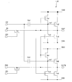
- FIG. 6 is a circuit diagram showing a configuration of the semiconductor device 1 described in Patent Document 2.
- the semiconductor device 1 includes a transistor Ta1, a transistor Ta2, a transistor Ta3, a transistor Ta4, a transistor Ta5, a transistor Tb1, a transistor Tb2, a transistor Tb3, a transistor Tb4, a transistor Tb5, a capacitor Ca1, and a capacitor Cb1.
- All the transistors are n-channel MOS transistors.
- the semiconductor device 1 is configured as a memory circuit including transistors of the same power supply type.
- the semiconductor device 1 has a configuration that can be connected to the power supply VDD and the power supply VSS.
- the power supply VDD is a positive potential and the power supply VSS is GND, but the present invention is not limited to this.
- the semiconductor device 1 receives the input signal IN, the inverted input signal INB (inverted signal of the input signal IN), the clock signal CK, and the enable signal EN, and the output signal OUT and the inverted output signal OUTB (output signal OUT). Inverted signal) is output.
- the input signal IN, the inverted input signal INB, the clock signal CK, the enable signal EN, the output signal OUT, and the inverted output signal OUTB are at a high level when active and at a low level when inactive. In the following, it is assumed that when it is high level, it is equal to the potential of the power supply VDD, and when it is low level, it is equal to the potential of the power supply VSS.
- the input signal IN, the inverted input signal INB, the clock signal CK, the enable signal EN, the output signal OUT, and the inverted output signal OUTB are input signals or output signals via terminals (electrodes), and therefore, for convenience of explanation.
- the input terminal IN, the inverting input terminal INB, the clock terminal CK, the enable terminal EN, the output terminal OUT, and the inverting output terminal OUTB are also referred to as appropriate.
- the transistor Ta1 has a drain terminal connected to the power supply VDD and a gate terminal connected to the source terminal of the transistor Ta5 and the output terminal OUT.
- the transistor Ta1 has a source terminal connected to the gate terminal of the transistor Ta2 and the drain terminal of the transistor Ta3, and is connected to the clock terminal CK via the capacitor Ca1.
- the transistor Ta2 has a drain terminal connected to the power supply VDD and a source terminal connected to the drain terminal of the transistor Ta4 and the output terminal OUT.
- the transistor Ta3 has a gate terminal connected to the inverted output terminal OUTB and a source terminal connected to the power supply VSS.
- the transistor Ta4 has a gate terminal connected to the inverted output terminal OUTB and a source terminal connected to the power supply VSS.
- the transistor Ta5 has a drain terminal connected to the input terminal IN and a gate terminal connected to the enable terminal EN.
- the transistor Tb1 has a drain terminal connected to the power supply VDD and a gate terminal connected to the source terminal of the transistor Tb5 and the inverted output terminal OUTB.
- the transistor Tb1 has a source terminal connected to the gate terminal of the transistor Tb2 and the drain terminal of the transistor Tb3, and is connected to the clock terminal CK via the capacitor Cb1.
- the transistor Tb2 has a drain terminal connected to the power supply VDD and a source terminal connected to the drain terminal of the transistor Tb4 and the inverted output terminal OUTB.
- the transistor Tb3 has a gate terminal connected to the output terminal OUT and a source terminal connected to the power supply VSS.
- the transistor Tb4 has a gate terminal connected to the output terminal OUT and a source terminal connected to the power supply VSS.
- the transistor Tb5 has a drain terminal connected to the inverting input terminal INB and a gate terminal connected to the enable terminal EN.
- connection point of the transistors Ta1, Ta2, Ta3 and the capacitor Ca1 is a node na1.
- a connection point of the transistors Tb1, Tb2, Tb3 and the capacitor Cb1 is a node nb1.
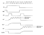
- FIG. 7 is a timing chart showing waveforms of various signals in the semiconductor device 1.
- VDD high level
- VSS low level
- the clock signal CK has a waveform that periodically repeats a high level and a low level, and is input at a higher frequency than the output signal OUT and the inverted output signal OUTB.
- the transistor Ta5 is turned on and the input signal IN is at a high level, the transistor Ta1 is turned on.
- the threshold voltage of the transistor Ta1 is Vth
- the potential of the node na1 becomes VDD ⁇ Vth (precharge operation).
- the transistor Ta2 is turned on.
- the transistor Ta5 and the transistor Ta1 are turned off, and the node na1 enters a floating state while holding the high level charge.
- the clock signal CK becomes a high level
- the potential of the node na1 is increased by the ⁇ potential by the clock signal CK and becomes VDD ⁇ Vth + ⁇ .
- this potential exceeds VDD + Vth
- the transistor Ta2 outputs VDD to the output terminal OUT.
- the transistor Ta1 Since the output terminal OUT and the gate terminal of the transistor Ta1 are connected to each other, the transistor Ta1 is turned on when the potential of the node na1 becomes VDD ⁇ Vth or less while the output signal OUT is at a high level. become. Note that when the potential of the node na1 is equal to or higher than VDD ⁇ Vth, the transistor Ta1 is turned off and the node na1 is in a floating state.
- the potential of the node na1 is charged again to VDD ⁇ Vth by the transistor Ta1 (refresh operation) even if the potential of the node na1 decreases due to off-leakage or the like.
- the potential of the node na1 can be pushed up to VDD ⁇ Vth + ⁇ , so that the output signal OUT can stably output VDD.
- the transistors Tb3 and Tb4 are turned on while the high-level output signal OUT is being output. As a result, the charge at the node nb1 is discharged, and the inverted output signal OUTB becomes low level.
- the transistor Tb5 is turned on and the inverted input signal INB is at the high level, the transistor Tb1 is turned on. Accordingly, when the threshold voltage of the transistor Tb1 is Vth, the potential of the node nb1 becomes VDD ⁇ Vth (precharge operation). When the potential of the node nb1 rises, the transistor Tb2 is turned on.
- the transistor Tb5 and the transistor Tb1 are turned off, and the node nb1 is in a floating state while holding the high level charge.
- the clock signal CK becomes a high level
- the potential of the node nb1 is increased by the ⁇ potential by the clock signal CK and becomes VDD ⁇ Vth + ⁇ .
- this potential exceeds VDD + Vth
- the transistor Tb2 outputs VDD to the inverting output terminal OUTB.
- the inverted output signal OUTB outputs a high level
- the potential of the node nb1 is charged again to VDD ⁇ Vth by the transistor Tb1 (refresh operation) even if the potential of the node nb1 decreases due to off-leakage or the like. Accordingly, during the period in which the clock signal CK is outputting a high level, the potential of the node nb1 can be pushed up to VDD ⁇ Vth + ⁇ , so that the inverted output signal OUTB can stably output VDD. .
- the transistors Ta3 and Ta4 are turned on while the high level inverted output signal OUTB is output. As a result, the charge of the node na1 is discharged and the output signal OUT is at a low level.
- they are alternately switched according to the timing when the enable signal EN becomes high level.
- the amplitude of the clock signal CK, the capacitance Ca1, and the capacitance Cb1 are set so that the potentials (VDD ⁇ Vth + ⁇ ) of the pushed up nodes na1 and nb1 are equal to or higher than VDD + Vth.
- the semiconductor device 1 since the frequency of the clock signal CK is set higher than the frequencies of the output signal OUT and the inverted output signal OUTB, even if the potentials of the nodes na1 and nb1 decrease due to off-leakage or the like. Then, until the enable signal EN becomes the high level next time, the potentials of the nodes na1 and nb1 can be pushed up to VDD + Vth or more by the pushing-up operation by the clock signal CK. That is, the semiconductor device 1 raises the potential levels of the nodes na1 and nb1 so as to satisfy a sufficient potential level by the bootstrap operation.
- Japanese Patent Publication Japanese Patent Laid-Open No. 63-292772 (published on November 30, 1988)” International Publication No. 2009/084272 Pamphlet (released on July 9, 2009)
- the semiconductor device 1 since the capacitors Ca1 and Cb1 are mounted in order to obtain the bootstrap operation, the semiconductor device 1 has a problem that the layout area increases as the capacitors Ca1 and Cb1 are formed.
- FIG. 8 shows a layout pattern of the semiconductor device 1 in plan view.
- the capacitors Ca1 and Cb1 are arranged in a region between the wiring to which the clock signal CK is supplied and the wiring to which the power supply VDD is supplied in plan view.
- the layout area of the semiconductor device 1 is increased as compared with the case where no capacitor is formed.
- the bootstrap capacitance is not sufficiently large with respect to the gate input capacitance of the transistor to be connected or other parasitic capacitance such as wiring, the level rise due to bootstrap is insufficient. For this reason, a large layout area is required to ensure a sufficient capacity.
- the present invention has been made in view of the above-described conventional problems, and an object of the present invention is to provide a semiconductor device and a semiconductor device unit capable of reducing a layout area in a configuration including a transistor and a bootstrap capacitor.
- An active matrix substrate, a liquid crystal panel, and a liquid crystal display device are provided.
- a semiconductor device of the present invention is a semiconductor device including at least a transistor and a bootstrap capacitor, and includes a first electrode made of the same material as a channel layer of the transistor, A second electrode formed above the first electrode via an insulating film; and a control signal wiring formed above the second electrode via a second insulating film, the second electrode Is connected to the gate electrode of the transistor, the control signal wiring is supplied with an external control signal, and the capacitance is an overlapping portion of the first electrode, the first insulating film, and the second electrode
- the superposition part and the control signal wiring overlap each other in plan view.
- a layout space is consumed for forming the capacity.
- the overlapping portion is arranged so as to overlap the control signal wiring. Therefore, it is possible to reduce the layout space consumed only for the capacity formation. Therefore, in the semiconductor device of the present invention, the layout area can be reduced.
- a semiconductor device unit includes a plurality of the semiconductor devices, and the plurality of semiconductor devices share the control signal wiring.
- An active matrix substrate of the present invention is an active matrix substrate including a display unit and a drive driver, and the drive driver is monolithically formed.
- the drive driver includes the semiconductor device or the semiconductor device. It is characterized by the unit being configured.
- the liquid crystal panel of the present invention is characterized by comprising the above active matrix substrate.
- the liquid crystal display device of the present invention is characterized by comprising the above-mentioned liquid crystal panel.
- the semiconductor device of the present invention includes the first electrode made of the same material as the channel layer of the transistor, and the second electrode formed above the first electrode through the first insulating film. And a control signal wiring formed above the second electrode through a second insulating film, the second electrode being connected to the gate electrode of the transistor, and the control signal wiring having an external
- the capacitor is formed in the overlapping portion of the first electrode, the first insulating film, and the second electrode, and the overlapping portion and the control signal wiring overlap in a plan view. It has the composition which is.
- the semiconductor device unit of the present invention since the semiconductor device unit of the present invention, the active matrix substrate of the present invention, the liquid crystal panel of the present invention, and the liquid crystal display device of the present invention have the above semiconductor device, the layout area can be reduced. Thus, it is possible to reduce the frame size, reduce the size, and reduce the weight.
- FIG. 1 is a plan view showing a layout pattern according to an embodiment of a semiconductor device of the present invention.
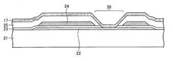
- FIG. 2 is a cross-sectional view taken along line A-A ′ of FIG. 1.
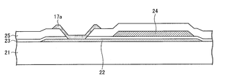
- FIG. 9 is a sectional view taken along line B-B ′ in FIG. 8.
- 1 is a plan view showing a layout pattern according to an embodiment of a semiconductor device unit of the present invention. It is a block diagram which shows one Embodiment of the liquid crystal display device in this invention. It is a circuit diagram which shows the structure of the conventional semiconductor device. 7 is a timing chart showing waveforms of various signals in the semiconductor device of FIG. 6.
- FIG. 7 is a plan view showing a layout pattern of the semiconductor device of FIG. 6.
- the present invention has a feature in a layout pattern in a semiconductor device including a transistor and a bootstrap capacitor, and this feature has an effect of reducing a layout area. Therefore, although details will be described later, the circuit configuration to which the present invention is applied is not limited as long as the circuit configuration is known as long as it is a semiconductor device including at least a transistor and a bootstrap capacitor. In other words, the present invention can be effective even when applied to a conventional semiconductor device having at least a transistor and a bootstrap capacitor.
- each embodiment will be described using a semiconductor device 10 having the same circuit configuration as that of the semiconductor device 1 shown in FIG. 6 in order to illustrate the effect of the present invention of reducing the layout area in an easy-to-understand manner. Since the semiconductor device 10 has the circuit configuration described in the background art above, description of the circuit configuration will be omitted as appropriate.
- FIG. 1 is a plan view showing a layout pattern in a plan view of the semiconductor device 10 of the present embodiment.
- the semiconductor device 10 includes a transistor Ta1, a transistor Ta2, a transistor Ta3, a transistor Ta4, a transistor Ta5, a transistor Tb1, a transistor Tb2, a transistor Tb3, a transistor Tb4, a transistor Tb5, a capacitor Ca1, and a capacitor Cb1. As shown in FIG. 1, these structures are formed on the substrate 21 and realized.
- Input wiring 14, output wiring 15 for outputting output signal OUT, output wiring 16 for outputting inverted output signal OUTB, clock signal wiring 17 to which clock signal CK is supplied, and enable signal EN Enable signal wiring 18 is formed.
- a semiconductor layer, a gate insulating film, a gate metal (hereinafter referred to as GM), an interlayer insulating film, and a source metal (hereinafter referred to as SM) are formed (stacked) in this order on the substrate 21. ) Is formed.
- These elements can be formed by, for example, a conventional general method of manufacturing a semiconductor device on a substrate monolithically.
- dotted portions indicate semiconductor layers
- hatched portions indicate GM
- gray portions indicate SM.
- the gate insulating film and the interlayer insulating film are transparent.
- transistors Ta1, Ta2, Ta3, Ta4, Ta5, Tb1, Tb2, Tb3, Tb4, Tb5, capacitors Ca1, Cb1, power supply wirings 11 and 12, input wirings 13 and 14, output wirings 15 and 14 16, a clock signal wiring 17 and an enable signal wiring 18 are formed.
- the semiconductor layer of each transistor corresponds to the semiconductor layer, the gate electrode corresponds to GM, and the drain electrode and source electrode correspond to SM.
- the semiconductor layer 22 of each capacitor corresponds to the semiconductor layer, and the capacitor electrode 24 corresponds to GM.
- the power supply wirings 11 and 12, the input wirings 13 and 14, and the clock signal wiring 17 correspond to SM.
- the output wirings 15 and 16 and the enable signal wiring 18 correspond to GM.
- the electrodes or layers of the same group (such as GM) are manufactured in the same manufacturing process and have the same thickness.
- the extending direction of the clock signal wiring 17 is the vertical direction, and the direction orthogonal thereto is the horizontal direction.
- these directions do not limit the actual use.
- the power supply wiring 11, the power supply wiring 12, and the clock signal wiring 17 are formed so as to extend in the vertical direction, and the clock signal wiring 17, the power supply wiring 11, and the power supply wiring 12 are arranged in the horizontal direction (here, from the left side to the right side). Arranged in order.
- the power supply wiring 11, the power supply wiring 12, and the clock signal wiring 17 have the same predetermined width, but are not limited thereto.
- the input wiring 13, the input wiring 14, and the enable signal wiring 18 are formed so as to extend in the lateral direction, and are arranged in a region on the opposite side of the clock signal wiring 17 from the power supply wiring 11 in plan view.
- the input wiring 13 is connected to the drain electrode of the transistor Ta5 through a contact hole.
- the input wiring 14 is connected to the drain electrode of the transistor Tb5 through a contact hole.
- the enable signal line 18 is connected to the gate electrode of the transistor Ta5 and the gate electrode of the transistor Tb5.
- the enable signal wiring 18 is illustrated as being formed at two locations, but is connected at a portion not illustrated.
- the input wiring 13, the input wiring 14, and the enable signal wiring 18 are narrower than the power supply wiring 11 and the like and have the same predetermined width, but are not limited thereto.
- the output wiring 15 and the output wiring 16 are formed so as to extend in the lateral direction, and are arranged so as to be orthogonal to the power supply wiring 12 in plan view.
- the output wiring 15 is connected to the source electrode of the transistor Ta2 through a lead wiring and a contact hole.
- the output wiring 16 is connected to the source electrode of the transistor Tb2 through a lead wiring and a contact hole.
- the output wiring 15 and the output wiring 16 are narrower than the power supply wiring 11 and have the same predetermined width, but are not limited thereto.
- the transistors other than the transistors Ta5 and Tb5 are laid out in a region between the power supply wiring 11 and the power supply wiring 12 in plan view, and the transistors Ta5 and Tb5 are in power supply of the clock signal wiring 17 in plan view. It is laid out in a region opposite to the wiring 11.
- the transistor Ta1 and the transistor Ta2 are arranged adjacent to each other in the horizontal direction, the transistor Ta1 is located on the power supply wiring 11 side, and the transistor Ta2 is located on the power supply wiring 12 side. Further, the transistor Ta1 and the transistor Ta2 are arranged so that the drain electrode and the source electrode face each other in the vertical direction, and the source electrode of the transistor Ta1 and the drain electrode of the transistor Ta2 are positioned on a line along the horizontal direction. is doing.
- the transistor Ta3 and the transistor Ta4 are arranged adjacent to each other in the horizontal direction, the transistor Ta3 is located on the power supply wiring 11 side, and the transistor Ta4 is located on the power supply wiring 12 side. Further, the transistor Ta3 and the transistor Ta4 are arranged so that the drain electrode and the source electrode face each other in the vertical direction, and the drain electrode of the transistor Ta3 and the drain electrode of the transistor Ta4 are positioned on a line along the horizontal direction. is doing.
- the transistor Ta5 is arranged in a region opposite to the power supply wiring 11 of the clock signal wiring 17 in plan view.
- the transistor Ta5 is arranged so that the drain electrode and the source electrode face each other in the vertical direction, and the source electrode of the transistor Ta5 is located near the line along the horizontal direction from the source electrode of the transistor Ta2.
- the transistor Tb1 and the transistor Tb2 are arranged adjacent to each other in the horizontal direction, the transistor Tb1 is located on the power supply wiring 11 side, and the transistor Tb2 is located on the power supply wiring 12 side. Further, the transistor Tb1 and the transistor Tb2 are arranged so that the drain electrode and the source electrode face each other in the vertical direction, and the source electrode of the transistor Tb1 and the drain electrode of the transistor Tb2 are positioned on a line along the horizontal direction. is doing.
- the transistor Tb3 and the transistor Tb4 are arranged adjacent to each other in the horizontal direction, the transistor Tb3 is located on the power supply wiring 11 side, and the transistor Tb4 is located on the power supply wiring 12 side.
- the transistor Tb3 and the transistor Tb4 are arranged so that the drain electrode and the source electrode face each other in the vertical direction, and the drain electrode of the transistor Tb3 and the drain electrode of the transistor Tb4 are positioned on a line along the horizontal direction. is doing.
- the transistor Tb5 is arranged in a region opposite to the power supply wiring 11 of the clock signal wiring 17 in plan view.
- the transistor Tb5 is disposed so that the drain electrode and the source electrode face each other in the vertical direction, and the source electrode of the transistor Tb5 is located near a line along the horizontal direction from the source electrode of the transistor Tb2.
- the transistor Ta1, the transistor Ta3, the transistor Tb1, and the transistor Tb3 are located on a line along the vertical direction.
- the transistor Ta2, the transistor Ta4, the transistor Tb2, and the transistor Tb4 are located on a line along the vertical direction.
- the transistor Ta5 and the transistor Tb5 are located on a line along the vertical direction.
- the transistor Ta1 is formed of a semiconductor layer, a gate insulating film, a gate electrode, an interlayer insulating film, a drain electrode, and a source electrode formed on the substrate 21.
- each region is formed from amorphous silicon, polysilicon, or the like so as to constitute an n-channel transistor.
- the gate insulating film is formed on the substrate 21 so as to cover the semiconductor layer.
- the gate insulating film is made of, for example, silicon nitride.
- the gate electrode is formed on the gate insulating film.
- the gate electrode is disposed so as to overlap a semiconductor layer (specifically, a channel formation region of the semiconductor layer) in plan view.
- the gate electrode may be made of, for example, a metal film such as titanium, chromium, aluminum, molybdenum, tantalum, tungsten, or copper, or an alloy film thereof, or a laminated film of the metal film and the alloy film. Also good.
- the interlayer insulating film is formed on the gate insulating film so as to cover the gate electrode.
- the interlayer insulating film is made of, for example, silicon nitride.
- the drain electrode and the source electrode are respectively formed on the interlayer insulating film.
- the drain electrode is disposed so as to overlap the semiconductor layer (specifically, the drain region of the semiconductor layer) in plan view, and is connected to the semiconductor layer through a contact hole.
- the source electrode is disposed so as to overlap the semiconductor layer (specifically, the source region of the semiconductor layer) in plan view, and is connected to the semiconductor layer through a contact hole.
- the drain electrode and the source electrode are arranged across the gate electrode in plan view.
- each transistor is electrically connected in accordance with the circuit configuration shown in FIG. 6 through a lead wiring (SM or GM) and a contact hole, which are appropriately arranged. Yes.
- SM or GM lead wiring
- the capacitor Ca1 and the capacitor Cb1 are arranged so as to overlap with the clock signal wiring 17 (control signal wiring) in plan view.
- the capacitor Cb1 includes a lead wire 19 provided so as to be electrically connected to the output wire 15 from the source electrode of the transistor Ta5, and a lead provided so as to be electrically connected to the output wire 16 from the source electrode of the transistor Tb5. It is arranged in a region between the wiring 20.
- the capacitor Ca1 is disposed in a region on the opposite side of the lead wire 19 from the capacitor Cb1 in plan view.
- FIG. 2 shows a cross-sectional structure of the formation region of the capacitor Cb1.
- FIG. 2 is a cross-sectional view taken along line A-A ′ of FIG.
- the semiconductor layer 22 (first electrode), the gate insulating film 23 (first insulating film), the capacitor electrode 24 (second electrode), the interlayer insulation are formed on the substrate 21.
- the film 25 (second insulating film) and the clock signal wiring 17 are stacked in this order.
- the semiconductor layer 22 is formed on the substrate 21.
- the semiconductor layer 22 has a rectangular shape in plan view, and is arranged in a region between the lead-out wiring 19 and the lead-out wiring 20 so that the longitudinal direction is along the clock signal wiring 17. That is, the semiconductor layer 22 is formed at a position away from the lead-out wiring 19 and the lead-out wiring 20 by a predetermined amount. In a plan view, the width of the semiconductor layer 22 in the short direction is larger than the width of the clock signal wiring 17.
- the semiconductor layer 22 is made of the same material as the semiconductor layer (channel layer) of each transistor.
- the gate insulating film 23 is formed on the substrate 21 so as to cover the semiconductor layer 22.
- This gate insulating film 23 is a gate insulating film used in a transistor.
- the capacitor electrode 24 is formed on the gate insulating film 23.
- the capacitor electrode 24 has a rectangular shape in plan view that is slightly smaller than the plan view shape of the semiconductor layer 22, and is disposed inside the semiconductor layer 22 and overlaps the semiconductor layer 22 in plan view. Yes. In plan view, the width of the capacitor electrode 24 in the short direction is larger than the width of the clock signal wiring 17.
- the capacitor electrode 24 is made of the same material as the gate electrode of each transistor.
- a clock signal wiring 17 is formed on the capacitor electrode 24 via an interlayer insulating film 25.
- This interlayer insulating film 25 is an interlayer insulating film used in a transistor. Further, the clock signal wiring 17 is connected to the semiconductor layer 22 through the contact hole 26. The clock signal wiring 17 is insulated from the capacitor electrode 24 by the interlayer insulating film 25.
- a capacitor that is, the capacitor Cb1 is formed in a portion (overlapping portion) overlapped by the semiconductor layer 22, the gate insulating film 23, and the capacitor electrode 24.
- the overlapping portion that becomes the capacitor Cb1 overlaps (overlaps) the clock signal wiring 17 in plan view.
- the clock signal wiring 17 exists entirely on the semiconductor layer 22, and the capacitor electrode 24 is located immediately below the clock signal wiring 17.
- FIG. 3 shows a cross-sectional structure of the capacitor Cb1 in the conventional layout pattern.
- 3 is a cross-sectional view taken along line B-B ′ of FIG.
- a portion 17a branched from the wiring to which the clock signal CK is supplied exists in a part on the semiconductor layer 22, and the capacitor electrode 24 is connected to the clock signal wiring 17 and It is not located directly under the portion 17a.
- the semiconductor device 10 includes a plurality of transistors and capacitors Ca1 and Cb1, and the semiconductor layer 22 is made of the same material as the channel layers of the plurality of transistors and is supplied with the clock signal CK.
- the clock signal wiring 17 is connected to the semiconductor layer 22 through the contact hole 26, the capacitor electrode 24 is connected to the gate electrode of the transistor, and the capacitors Ca1 and Cb1 are connected to the semiconductor layer 22, the gate insulating film 23, and the capacitor. It is formed in the overlapping portion of the electrode 24 and has a configuration in which the overlapping portion and the clock signal wiring 17 overlap in a plan view.
- the layout pattern of the present embodiment as shown in FIG. 1, the overlapping portion that becomes the capacitors Ca1 and Cb1 is arranged so as to overlap the clock signal wiring 17. Therefore, it is possible to reduce the layout space consumed only for forming the capacitors Ca1 and Cb1. Therefore, in the semiconductor device 10 to which the layout pattern of the present embodiment is applied, the layout area can be reduced. In this embodiment, the layout area can be reduced by about the width of the capacitors Ca1 and Cb1 in the short direction as compared with the conventional case.
- noise is generated in the wiring via the capacitors Ca1 and Cb1 as compared with the case where the capacitors Ca1 and Cb1 are overlaid on other wiring (for example, the power supply wiring 11). Can be suppressed (mixing, crosstalk, etc.), and malfunction caused by this can be prevented.
- the interlayer parasitic capacitance between the capacitor electrode 24 and the clock signal wiring 17 also functions as a bootstrap capacitor, the bootstrap effect can be enhanced if the capacitor formation region has the same area as the conventional one. Become.
- the capacitors Ca1 and Cb1 are formed so as to protrude slightly from the clock signal wiring 17 in plan view. In this way, by using the inter-wiring space between the clock signal wiring 17 and the power supply wiring 11, it is possible to secure a wide capacitance forming region.
- the size of the capacitance forming region (overlapping portion) may be determined according to a desired capacitance, and may be a size that can be directly below the clock signal wiring 17, and what is the shape in plan view? It may be a shape.
- the layout pattern shown in FIG. 1 is an example, and the layout of the portion not related to the feature that the formation region of the capacitors Ca1 and Cb1 and the clock signal wiring 17 overlap (for example, the relative arrangement of the transistors)
- the arrangement of the power supply wiring 12 and the like can be changed as appropriate.
- the widths of SM and GM are not limited to the sizes shown in FIG. However, generally, the width of SM is larger than that of GM, and among the SMs, the power supply wires 11 and 12 are provided so as to have a larger width than other wires.
- the formation regions of the transistors have the same size, but may have different sizes.
- the semiconductor layer and the wiring are connected by one contact hole, a plurality of contact holes may be formed depending on the size of the formation region of the semiconductor layer.
- the semiconductor device 10 has a configuration in which the bootstrap capacitor is formed by the clock signal CK.
- a signal that forms the bootstrap capacitor may be another control signal (for example, a signal for determining polarity, or another clock signal). Or a signal generated based on this).
- the control signal that contributes to the increase of the potential of the ⁇ potential is superimposed on the control signal wiring (SM) that supplies the capacitor for performing the bootstrap in a plan view, Good.
- SM control signal wiring
- the capacity of the semiconductor device may be one, or may be two or more.
- the signal wiring may be connected to the capacitor electrode instead of the semiconductor layer in the capacitor forming portion.
- a semiconductor device to which the present invention can be applied is not limited to a configuration in which the conductivity types of transistors are the same, and may be a configuration in which an n-channel type and a p-channel type are mixed.
- An n-channel transistor is turned on by a high-level signal and turned off by a low-level signal, and vice versa for a p-channel transistor.
- advantages such as low power consumption by forming the CMOS transistor, for example, while the process of forming the p-channel transistor and the n-channel transistor respectively. Therefore, there is a problem in that the manufacturing process becomes complicated and the manufacturing cost increases. Therefore, if a plurality of transistors having the same conductivity type are used, the manufacturing process can be simplified, and there is an advantage that the effect is great.
- the present invention is applicable to any semiconductor device including at least a transistor and a bootstrap capacitor.
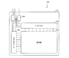
- FIG. 4 is a plan view showing a layout pattern in plan view of the semiconductor device unit 50 of the present embodiment.
- the semiconductor device unit 50 of the present embodiment includes a semiconductor device 10a and a semiconductor device 10b.
- the semiconductor device 10a and the semiconductor device 10b are arranged along the vertical direction.
- the semiconductor device 10a includes a transistor Ta11, a transistor Ta12, a transistor Ta13, a transistor Ta14, a transistor Ta15, a transistor Tb11, a transistor Tb12, a transistor Tb13, a transistor Tb14, a transistor Tb15, a capacitor Ca11, and a capacitor Cb11.
- 10 correspond to the transistors Ta1, Ta2, Ta3, Ta4, Ta5, Tb1, Tb2, Tb3, Tb4, Tb5, and the capacitors Ca1, Cb1.
- the semiconductor device 10a differs from the semiconductor device 10 having the layout pattern of the above-described embodiment in the place where the capacitor Ca11 and the capacitor Cb11 are laid out.
- the semiconductor device 10b includes a transistor Ta21, a transistor Ta22, a transistor Ta23, a transistor Ta24, a transistor Ta25, a transistor Tb21, a transistor Tb22, a transistor Tb23, a transistor Tb24, a transistor Tb25, a capacitor Ca21, and a capacitor Cb21.
- 10 correspond to the transistors Ta1, Ta2, Ta3, Ta4, Ta5, Tb1, Tb2, Tb3, Tb4, Tb5, and the capacitors Ca1, Cb1.
- the semiconductor device 10b differs from the semiconductor device 10 having the layout pattern of the above-described embodiment in the place where the capacitor Ca21 and the capacitor Cb21 are laid out.
- input wiring 14 output wiring 15a for outputting first output signal OUT1, output wiring 16a for outputting first inverted output signal OUTB1, and output wiring 15b for outputting second output signal OUT2.
- An output wiring 16b for outputting the second inverted output signal OUTB2 a clock signal wiring 17 to which the clock signal CK is supplied, a clock signal wiring 27 to which the inverted clock signal CKB (inverted signal of the clock signal CK) is supplied,
- the enable signal wiring 18a to which the 1 enable signal EN1 is input and the enable to which the second enable signal EN2 is input Signal lines 18b are formed.
- the power supply wiring 11, the power supply wiring 12, the clock signal wiring 17, and the clock signal wiring 27 are formed so as to extend in the vertical direction, and the power supply wiring 12 (one power supply wiring 12 in the horizontal direction (here, from left to right)).
- the clock signal wiring 27, the clock signal wiring 17, the power supply wiring 11, and the power supply wiring 12 are arranged in this order.
- the power supply wiring 12 is illustrated as being formed at two locations, but is connected at a portion not illustrated.
- the power supply wiring 11, the power supply wiring 12, the clock signal wiring 17, and the clock signal wiring 27 have the same predetermined width, but are not limited thereto.
- the input wiring 13, the input wiring 14, the enable signal wiring 18 a, and the enable signal wiring 18 b are formed so as to extend in the lateral direction, and are regions on the opposite side of the one power supply wiring 12 from the clock signal wiring 27 in plan view. Is arranged.
- the input wiring 13 is connected to the drain electrode of the transistor Ta15 and the drain electrode of the transistor Ta25.
- the input wiring 14 is connected to the drain electrode of the transistor Tb15 and the drain electrode of the transistor Tb25.
- the enable signal line 18a is connected to the gate electrode of the transistor Ta15 and the gate electrode of the transistor Tb15.
- the enable signal line 18b is connected to the gate electrode of the transistor Ta25 and the gate electrode of the transistor Tb25, respectively.
- the input wiring 13, the input wiring 14, the enable signal wiring 18 a, and the enable signal wiring 18 b are illustrated as being formed at two locations, but each is connected at a portion not illustrated. Yes.
- the input wiring 13, the input wiring 14, the enable signal wiring 18a, and the enable signal wiring 18b are narrower than the power supply wiring 11 and the like and have the same predetermined width, but are not limited thereto.
- the output wiring 15a, the output wiring 16a, the output wiring 15b, and the output wiring 16b are formed so as to extend in the lateral direction, and are arranged so as to be orthogonal to the other power supply wiring 12 in plan view.
- the output wiring 15a is connected to the source electrode of the transistor Ta12 through a lead wiring and a contact hole.
- the output wiring 16a is connected to the source electrode of the transistor Tb12 via a lead wiring and a contact hole.
- the output wiring 15b is connected to the source electrode of the transistor Ta22 through a lead wiring and a contact hole.
- the output wiring 16b is connected to the source electrode of the transistor Tb22 through a lead wiring and a contact hole.
- the output wiring 15a, the output wiring 16a, the output wiring 15b, and the output wiring 16b are narrower than the power supply wiring 11 and have the same predetermined width, but are not limited thereto.
- Each transistor other than the transistors Ta15, Tb15, Ta25, and Tb25 is laid out in a region between the power supply wiring 11 and one power supply wiring 12 in a plan view, and the transistors Ta15, Tb15, Ta25, and Tb25 are In plan view, the other power supply wiring 12 is laid out in a region opposite to the clock signal wiring 17.
- the first output signal OUT1, the first inverted output signal OUTB1, the second output signal OUT2, and the second enable signal EN1 and the second enable signal EN2 are activated in accordance with the timing of activating the first enable signal EN1 and the second enable signal EN2, respectively.
- the inverted output signal OUTB2 can be sequentially output.
- an inverted clock signal CKB is supplied instead of the clock signal CK.
- the formation region of the capacitor Ca11 and the capacitor Cb11 is arranged so as to overlap the clock signal wiring 17 (control signal wiring) and the power supply wiring 11 (metal wiring) in plan view.
- a clock signal wiring 17 and a power supply wiring 11 exist via an interlayer insulating film 25.
- the semiconductor layer 22 is connected to the clock signal wiring 17 through the contact hole 26.
- the capacitors Ca11 and Cb11 are formed in a portion (overlapping portion) overlapped by the semiconductor layer 22, the gate insulating film 23, and the capacitor electrode 24.
- the formation region of the capacitor Ca11 and the capacitor Cb11 is larger than the formation region of the capacitor Ca1 and the capacitor Cb1 of the above embodiment.
- the formation region of the capacitor Ca21 and the capacitor Cb21 is arranged so as to overlap with one power supply wiring 12 (metal wiring) and the clock signal wiring 27 (control signal wiring) in plan view.
- one power supply wiring 12 and a clock signal wiring 27 exist via an interlayer insulating film 25.
- the semiconductor layer 22 is connected to the clock signal wiring 27 through the contact hole 26.
- the capacitors Ca21 and Cb21 are formed in a portion (overlapping portion) overlapped by the semiconductor layer 22, the gate insulating film 23, and the capacitor electrode 24.
- the formation region of the capacitor Ca21 and the capacitor Cb21 is larger than the formation region of the capacitor Ca1 and the capacitor Cb1 of the above embodiment, and is the same as the formation region of the capacitor Ca11 and the capacitor Cb11.
- the overlapping portion that becomes the capacitors Ca11 and Cb11 overlaps the clock signal wiring 17 and the power supply wiring 11, and the overlapping portion that becomes the capacitors Ca21 and Cb21 is the one power supply wiring 12. In addition, it overlaps the clock signal wiring 27. If the power supply VDD is stable, the concern about noise superposition can be eliminated.
- the influence of noise can be ignored and the formation region of the capacitors Ca1 and Cb1 can be overlaid on the power supply wiring 11, so that the space can be used effectively. Therefore, it is possible to efficiently use the layout space and reduce the layout space consumed only for forming the capacitors Ca11, Cb11, Ca21, and Cb21. Therefore, in the semiconductor device unit 50, the layout area can be reduced.
- the semiconductor device unit 50 it is possible to secure a large capacitance forming region while suppressing an increase in layout space, and a sufficient potential increase (bootstrap amount) can be obtained.
- the layout pattern of this example can be similarly applied to the layout pattern of the semiconductor device 10 of the first embodiment.
- the semiconductor device unit 50 includes the semiconductor device 10a and the semiconductor device 10b, three or more semiconductor devices may be provided. In this case, it is desirable to share the power supply wiring and the clock signal wiring in order to reduce the layout space.
- the capacitance forming region is overlapped with two SMs.
- the overlapping portion may be overlapped with three or more SMs. Note that it is not necessary to overlap all three or more SMs, and any one of them can be stacked according to a desired capacity. In this way, the layout space can be used efficiently.
- FIG. 5 is a block diagram schematically showing a configuration example of the liquid crystal display device 100 of the present embodiment.
- the liquid crystal display device 100 includes a display unit 102, a source driver 103 (drive driver), a gate / CS driver 104 (drive driver), and a buffer circuit 105 in a liquid crystal panel 101.
- the display unit 102 is provided with pixels arranged in an array. Further, the display portion 102 is provided with a source line, a gate line, and a CS line corresponding to each pixel.
- the source driver 103 sequentially outputs a data signal for writing to each pixel to each source line of the display unit 102.
- the gate / CS driver 104 sequentially outputs a selection signal (scanning signal) for selecting a pixel to which the data signal from the source driver 103 is written to each gate line of the display unit 102, and also an auxiliary capacitor (CS capacitor).
- a CS signal is output to the CS line, which is a potential supply line to.
- the buffer circuit 105 converts various control signals (for example, a clock signal CK, a start pulse SP, an initialization signal INI, a polarity determination signal, etc.) sent from an external display controller or the like into a low output impedance signal,
- the source driver 103 and the gate / CS driver 104 are supplied.
- the semiconductor device 10 or the semiconductor device unit 50 of the above-described embodiment can be applied to each part.
- it can be suitably used for a shift register or an output unit in the source driver 103 and the gate / CS driver 104.
- a semiconductor device including a transistor and a bootstrap capacitor is widely used.
- the shift register is configured by a circuit including a CMOS transistor and a boot slap capacitor, or a circuit including a transistor of the same conductivity type and a boot slap capacitor.
- the effects produced by the semiconductor device 10 or the semiconductor device unit 50 of the above-described embodiment can be obtained in each part, and as a whole, the frame can be reduced in size, size, and weight. It becomes possible.
- the liquid crystal panel 101 has a configuration in which a liquid crystal layer is sandwiched between two substrates facing each other.
- One substrate is a substrate on which a common electrode or the like is formed
- the other substrate is a substrate (an active matrix substrate) on which the display unit 102 or the like is formed.
- the peripheral circuits such as the source driver 103, the gate / CS driver 104, and the buffer circuit 105 may be monolithically formed on the active matrix substrate.
- the layout area can be reduced, so that it is possible to further reduce the frame size, size, and weight.
- the configuration of the liquid crystal display device 100 described above is schematic, and other conventional configurations may be provided.
- a backlight or a display controller can be provided.
- a power supply circuit for generating a power supply for a logic circuit, a reference voltage of a data signal, a counter voltage, an auxiliary capacitance voltage, and the like may be provided.
- a demultiplexer may be configured instead of the source driver 103.
- the semiconductor device of the present invention is a semiconductor device including at least a transistor and a bootstrap capacitor, and includes the first electrode made of the same material as the channel layer of the transistor and the first insulating film via the first insulating film.
- a control signal from the outside is supplied to the control signal wiring
- the capacitor is formed in an overlapping portion of the first electrode, the first insulating film, and the second electrode, and is seen in a plan view.
- the superimposing unit and the control signal wiring overlap each other.
- control signal is preferably a clock signal.
- control signal wiring is connected to the first electrode through a contact hole.
- a plurality of the capacitors may be provided, and the control signal wiring may have an overlapping portion in each capacitor.
- the semiconductor device of the present invention further includes a metal wiring formed on the same layer as the control signal wiring so as to be adjacent to the control signal wiring, and the overlapping portion in plan view includes the control signal wiring and the control signal wiring. It is preferable to overlap the metal wiring. According to this, it is possible to ensure a wide overlapping portion by efficiently using the layout space.
- a plurality of the capacitors may be provided, and the control signal wiring and the metal wiring may be configured such that overlapping portions of the capacitors overlap.
- the semiconductor device of the present invention it is preferable that a plurality of the metal wirings are provided.
- the present invention can be suitably used not only in a field related to a semiconductor device including at least a transistor and a bootstrap capacitor, but also in a field related to a method for manufacturing a semiconductor device, and further includes a semiconductor device. It can also be widely used in the fields of liquid crystal panels and liquid crystal display devices including the same.
Landscapes
- Engineering & Computer Science (AREA)
- Chemical & Material Sciences (AREA)
- Crystallography & Structural Chemistry (AREA)
- Physics & Mathematics (AREA)
- Computer Hardware Design (AREA)
- General Physics & Mathematics (AREA)
- Theoretical Computer Science (AREA)
- Thin Film Transistor (AREA)
- Semiconductor Integrated Circuits (AREA)
- Power Engineering (AREA)
- Liquid Crystal (AREA)
Abstract
複数のトランジスタと容量(Ca1・Cb1)とを備える半導体装置(10)であって、トランジスタのチャネル層と同一材料で構成された半導体層(22)と、ゲート絶縁膜を介して半導体層(22)よりも上層に形成された容量電極(24)と、層間絶縁膜を介して容量電極(24)よりも上層に形成されたクロック信号配線(17)とを備え、容量電極(24)はトランジスタのゲート電極に接続され、クロック信号配線(17)には、外部からのクロック信号(CK)が供給され、容量(Ca1・Cb1)は、半導体層(22)、ゲート絶縁膜(23)、および容量電極(24)の重畳部に形成され、平面視において重畳部とクロック信号配線(17)とが重なっている。これにより、レイアウト面積の低減を図ることができる半導体装置、半導体装置ユニット、アクティブマトリクス基板、液晶パネル、および液晶表示装置を提供する。
Description
本発明は、トランジスタとブートストラップ用の容量とを備える半導体装置、半導体装置ユニット、アクティブマトリクス基板、液晶パネル、および液晶表示装置に関するものであり、特に、レイアウト面積の低減を図る技術に関するものである。
液晶表示装置には、駆動ドライバなどの周辺回路を表示部と同一基板上に作り込んだ液晶パネルを搭載するものがある。このような液晶パネルを備える液晶表示装置では、ガラス基板の外部に周辺回路を実現するICが配置されていた従来の液晶表示装置と比べて、パネル実装工程の簡略化や、実装領域の削減による狭額縁化、小型化、軽量化などが可能となっている。
上記周辺回路としては、ゲートドライバ、CSドライバ、およびソースドライバなどの駆動ドライバの他に、バッファ回路やレベルシフタ回路などがある。これらの周辺回路は、トランジスタなどを備えた半導体回路(半導体装置)により構成されている。
ここで、トランジスタは所定の閾値電圧を有している。このため、トランジスタの出力信号は、自身の閾値電圧により生じる電圧降下の分、電位レベルが低下する。よって、トランジスタから所望の電位レベルで出力を行うためには、上記閾値電圧を考慮して回路構成を設計する必要があった。上記周辺回路は、後段の回路を誤動作無く安定して動作させ、表示部に配列された各画素を正常に順次駆動するために、所定の電位レベルで出力を行うことが求められる。
そこで、十分な電位レベルを満たすように信号の電位レベルを上昇させる(突き上げる)、ブートストラップ動作という技術が提案されている(例えば、特許文献1および2参照)。
以下、特許文献2に記載の半導体装置を参照して、ブートストラップ動作について説明する。
図6は、特許文献2に記載の半導体装置1の構成を示す回路図である。図6に示すように、半導体装置1は、トランジスタTa1、トランジスタTa2、トランジスタTa3、トランジスタTa4、トランジスタTa5、トランジスタTb1、トランジスタTb2、トランジスタTb3、トランジスタTb4、トランジスタTb5、容量Ca1、および容量Cb1を備えている。各トランジスタは全て、nチャネル型のMOSトランジスタである。半導体装置1は、同一電源型のトランジスタを備えるメモリ回路として構成されている。
また、半導体装置1は、電源VDDおよび電源VSSに接続可能な構成を有している。例えば、電源VDDは正電位となり、電源VSSはGNDとなるが、これに限らない。
さらに、半導体装置1は、入力信号IN、反転入力信号INB(入力信号INの反転信号)、クロック信号CK、およびイネーブル信号ENが入力されるとともに、出力信号OUTおよび反転出力信号OUTB(出力信号OUTの反転信号)を出力する構成を有している。入力信号IN、反転入力信号INB、クロック信号CK、イネーブル信号EN、出力信号OUT、および反転出力信号OUTBは、アクティブのときにハイレベルとなり、非アクティブのときローレベルとなる。以下では、ハイレベルのときは電源VDDの電位に等しく、ローレベルのときは電源VSSの電位に等しいとする。
なお、入力信号IN、反転入力信号INB、クロック信号CK、イネーブル信号EN、出力信号OUT、および反転出力信号OUTBは、端子(電極)を介した入力信号または出力信号であるため、説明の便宜上、以下では適宜、入力端子IN、反転入力端子INB、クロック端子CK、イネーブル端子EN、出力端子OUT、および反転出力端子OUTBとも呼ぶこととする。
トランジスタTa1は、ドレイン端子が電源VDDに接続され、ゲート端子がトランジスタTa5のソース端子および出力端子OUTに接続されている。また、トランジスタTa1は、ソース端子がトランジスタTa2のゲート端子およびトランジスタTa3のドレイン端子に接続されるとともに、容量Ca1を介してクロック端子CKに接続されている。トランジスタTa2は、ドレイン端子が電源VDDに接続され、ソース端子がトランジスタTa4のドレイン端子および出力端子OUTに接続されている。トランジスタTa3は、ゲート端子が反転出力端子OUTBに接続され、ソース端子が電源VSSに接続されている。トランジスタTa4は、ゲート端子が反転出力端子OUTBに接続され、ソース端子が電源VSSに接続されている。トランジスタTa5は、ドレイン端子が入力端子INに接続され、ゲート端子がイネーブル端子ENに接続されている。
トランジスタTb1は、ドレイン端子が電源VDDに接続され、ゲート端子がトランジスタTb5のソース端子および反転出力端子OUTBに接続されている。また、トランジスタTb1は、ソース端子がトランジスタTb2のゲート端子およびトランジスタTb3のドレイン端子に接続されるとともに、容量Cb1を介してクロック端子CKに接続されている。トランジスタTb2は、ドレイン端子が電源VDDに接続され、ソース端子がトランジスタTb4のドレイン端子および反転出力端子OUTBに接続されている。トランジスタTb3は、ゲート端子が出力端子OUTに接続され、ソース端子が電源VSSに接続されている。トランジスタTb4は、ゲート端子が出力端子OUTに接続され、ソース端子が電源VSSに接続されている。トランジスタTb5は、ドレイン端子が反転入力端子INBに接続され、ゲート端子がイネーブル端子ENに接続されている。
なお、トランジスタTa1,Ta2,Ta3、並びに容量Ca1の接続点を、ノードna1とする。トランジスタTb1,Tb2,Tb3、並びに容量Cb1の接続点を、ノードnb1とする。
次いで、上記構成を有する半導体装置1の動作を説明する。
図7は、半導体装置1における各種信号の波形を示すタイミングチャートである。ここでは、ハイレベル(VDD)の出力信号OUTを出力するとともに、ローレベル(VSS)の反転出力信号OUTBを出力する期間Aの後、ローレベルの出力信号OUTを出力するとともに、ハイレベルの反転出力信号OUTBを出力する期間Bに移行する場合について説明する。
(期間A)
クロック信号CKが入力された状態の半導体装置1において、入力信号INがハイレベル、かつ、反転入力信号INBがローレベルになり、続いてイネーブル信号ENがハイレベルになると、トランジスタTa5・Tb5がオンになる。クロック信号CKは、ハイレベルとローレベルとを周期的に繰り返す波形を示し、出力信号OUTおよび反転出力信号OUTBよりも高い周波数で入力される。
クロック信号CKが入力された状態の半導体装置1において、入力信号INがハイレベル、かつ、反転入力信号INBがローレベルになり、続いてイネーブル信号ENがハイレベルになると、トランジスタTa5・Tb5がオンになる。クロック信号CKは、ハイレベルとローレベルとを周期的に繰り返す波形を示し、出力信号OUTおよび反転出力信号OUTBよりも高い周波数で入力される。
このとき、トランジスタTa5がオン、かつ、入力信号INはハイレベルであるので、トランジスタTa1がオンとなる。これにより、トランジスタTa1の閾値電圧をVthとすると、ノードna1の電位は、VDD-Vthになる(プリチャージ動作)。ノードna1の電位が上昇すると、トランジスタTa2はオンになる。
続いて、イネーブル信号ENがハイレベルからローレベルになると、トランジスタTa5およびトランジスタTa1がオフとなり、ノードna1はハイレベルの電荷を保持したままフローティング状態になる。この状態で、クロック信号CKがハイレベルになると、クロック信号CKにより、ノードna1の電位は、α電位分突き上げられ、VDD-Vth+αになる。この電位がVDD+Vthを超える場合は、トランジスタTa2は、出力端子OUTにVDDを出力する。
このように、ノードna1の電位がクロック信号CKによって突き上げられているときは、トランジスタTa2のゲート端子には高電位の信号が入力される。よって、トランジスタTa2から出力端子OUTに、VDDの電位レベルの信号、すなわち閾値落ちしない信号が出力される。
なお、イネーブル信号ENが一旦ハイレベルになると、その後、イネーブル信号ENがローレベルになっても、出力信号OUTがハイレベルであれば、トランジスタTa1のゲート端子に、常にハイレベルの信号を入力することができる。これにより、ハイレベルの出力信号OUTを保持し続けることができる。
また、出力端子OUTおよびトランジスタTa1のゲート端子が互いに接続されているので、出力信号OUTがハイレベルを出力している間は、ノードna1の電位がVDD-Vth以下になると、トランジスタTa1はオン状態になる。なお、ノードna1の電位がVDD-Vth以上の電位のときには、トランジスタTa1はオフ状態になり、ノードna1はフローティング状態になる。
これにより、出力信号OUTがハイレベルを出力している間は、ノードna1の電位は、オフリークなどにより低下したとしても、トランジスタTa1により再びVDD-Vthまでチャージされる(リフレッシュ動作)。これにより、クロック信号CKがハイレベルを出力している期間中は、ノードna1の電位を、VDD-Vth+αまで突き上げることができるため、出力信号OUTは、安定してVDDを出力することができる。
一方、ハイレベルの出力信号OUTが出力されている間、トランジスタTb3・Tb4がオンになる。これにより、ノードnb1の電荷はディスチャージされるとともに、反転出力信号OUTBはローレベルとなる。
(期間B)
続いて、入力信号INがローレベル、かつ、反転入力信号INBがハイレベルになり、続いてイネーブル信号ENがハイレベルになると、トランジスタTa5・Tb5がオンになる。
続いて、入力信号INがローレベル、かつ、反転入力信号INBがハイレベルになり、続いてイネーブル信号ENがハイレベルになると、トランジスタTa5・Tb5がオンになる。
このとき、トランジスタTb5がオン、かつ、反転入力信号INBはハイレベルであるので、トランジスタTb1がオンとなる。これにより、トランジスタTb1の閾値電圧をVthとすると、ノードnb1の電位は、VDD-Vthになる(プリチャージ動作)。ノードnb1の電位が上昇すると、トランジスタTb2はオンになる。
続いて、イネーブル信号ENがハイレベルからローレベルになると、トランジスタTb5およびトランジスタTb1がオフとなり、ノードnb1はハイレベルの電荷を保持したままフローティング状態になる。この状態で、クロック信号CKがハイレベルになると、クロック信号CKにより、ノードnb1の電位は、α電位分突き上げられ、VDD-Vth+αになる。この電位がVDD+Vthを超える場合は、トランジスタTb2は、反転出力端子OUTBにVDDを出力する。
このように、ノードnb1の電位がクロック信号CKによって突き上げられているときは、トランジスタTb2のゲート端子には高電位の信号が入力される。よって、トランジスタTb2から反転出力端子OUTBに、VDDの電位レベルの信号、すなわち閾値落ちしない信号が出力される。
なお、上述と同様に、イネーブル信号ENが一旦ハイレベルになると、その後、イネーブル信号ENがローレベルになっても、反転出力信号OUTBがハイレベルであれば、トランジスタTb1のゲート端子に、常にハイレベルの信号を入力することができる。これにより、ハイレベルの反転出力信号OUTBを保持し続けることができる。
また、反転出力信号OUTBがハイレベルを出力している間は、ノードnb1の電位は、オフリークなどにより低下したとしても、トランジスタTb1により再びVDD-Vthまでチャージされる(リフレッシュ動作)。これにより、クロック信号CKがハイレベルを出力している期間中は、ノードnb1の電位を、VDD-Vth+αまで突き上げることができるため、反転出力信号OUTBは、安定してVDDを出力することができる。
一方、ハイレベルの反転出力信号OUTBが出力されている間、トランジスタTa3・Ta4がオンになる。これにより、ノードna1の電荷はディスチャージされるとともに、出力信号OUTはローレベルとなる。
このようにして、ハイレベルの出力信号OUT、かつ、ローレベルの反転出力信号OUTBを出力する期間Aと、ローレベルの出力信号OUT、かつ、ハイレベルの反転出力信号OUTBを出力する期間Bとが、イネーブル信号ENがハイレベルになるタイミングに応じて交互に切り替わる。出力信号OUTおよび反転出力信号OUTBは、一方がVDDを出力しているときには、他方はVSSを出力する。
なお、クロック信号CKの振幅、容量Ca1、および容量Cb1は、突き上げられたノードna1・nb1の電位(VDD-Vth+α)が、VDD+Vth以上になるように設定される。
以上のように、半導体装置1では、クロック信号CKの周波数が、出力信号OUTおよび反転出力信号OUTBの周波数よりも高く設定されているため、オフリークなどによりノードna1・nb1の電位が低下しても、次にイネーブル信号ENがハイレベルになるまでの間に、ノードna1・nb1の電位を、クロック信号CKによる突き上げ動作によりVDD+Vth以上に突き上げることができる。つまりは、半導体装置1は、ブートストラップ動作によって、ノードna1・nb1の電位レベルを十分な電位レベルを満たすように上昇させている。
したがって、出力端子OUTおよび反転出力端子OUTBから、安定してVDDを出力することが可能となる。これにより、出力端子OUTおよび反転出力端子OUTBに接続される後段の回路は、安定した動作を得ることが可能となる。
しかしながら、上記の半導体装置1では、ブートストラップ動作を得るために容量Ca1・Cb1を搭載しているため、容量Ca1・Cb1を形成する分、レイアウト面積が増加するという問題を有している。
図8に、半導体装置1の平面視でのレイアウトパターンを示す。図8に示すように、ノイズの影響を避けるため、容量Ca1・Cb1は、平面視で、クロック信号CKが供給される配線と電源VDDが供給される配線との間の領域に配置されている。この図面によれば、半導体装置1では、容量を形成しない場合と比較してレイアウト面積が増加していることが明らかに分かる。また、ブートストラップ用の容量は、接続先のトランジスタのゲート入力容量やその他配線などの寄生容量に対して十分大きな容量でなければ、ブートストラップによるレベル上昇が不十分となる。このため、十分な容量を確保するために大きなレイアウト面積を必要とする。
また、製品の小型化(液晶パネルの狭額縁化)や、製品のデザイン上の制約により、必要な容量を形成するためのスペースの確保が困難な状況が発生することもある。レイアウト面積の制約の問題は、必要な容量が大きいほど顕著になる。
本発明は、上記従来の問題点に鑑みなされたものであって、その目的は、トランジスタとブートストラップ用の容量とを備える構成において、レイアウト面積の低減を図ることができる半導体装置、半導体装置ユニット、アクティブマトリクス基板、液晶パネル、および液晶表示装置を提供することにある。
本発明の半導体装置は、上記課題を解決するために、少なくともトランジスタおよびブートストラップ用の容量を備える半導体装置であって、上記トランジスタのチャネル層と同一材料で構成された第1電極と、第1絶縁膜を介して上記第1電極よりも上層に形成された第2電極と、第2絶縁膜を介して上記第2電極よりも上層に形成された制御信号配線とを備え、上記第2電極は、上記トランジスタのゲート電極に接続され、上記制御信号配線には、外部からの制御信号が供給され、上記容量は、上記第1電極、上記第1絶縁膜、および上記第2電極の重畳部に形成され、平面視において上記重畳部と上記制御信号配線とが重なっていることを特徴としている。
通常、容量を備えた半導体装置においては、容量を形成する分、レイアウトスペースを消費する。これに対し、上記の構成によるレイアウトパターンでは、重畳部は制御信号配線と重なって配置されている。よって、容量の容量形成のためだけに消費されるレイアウトスペースを低減することが可能となる。したがって、本発明の半導体装置では、レイアウト面積の低減を図ることが可能となる。
また、上記の構成によれば、ブートストラップ動作によってトランジスタのゲート電極の電位を上昇させることにより、該トランジスタから閾値落ちしない信号を出力することが可能となる。この際、ブートストラップによるレベル上昇を十分に行わせるためには、大きな容量が必要となり、容量によるレイアウト面積の増加が顕著となる。よって、上記の構成によれば、特にレイアウト面積低減効果を得ることが可能となる。
本発明の半導体装置ユニットは、上記の半導体装置を複数備え、上記複数の半導体装置が、上記制御信号配線を共用していることを特徴としている。
本発明のアクティブマトリクス基板は、表示部と駆動ドライバとを備え、上記駆動ドライバがモノリシックに形成されたアクティブマトリクス基板であって、上記駆動ドライバには、上記の半導体装置、または、上記の半導体装置ユニットが構成されていることを特徴としている。
本発明の液晶パネルは、上記のアクティブマトリクス基板を備えることを特徴としている。
本発明の液晶表示装置は、上記の液晶パネルを備えることを特徴としている。
以上のように、本発明の半導体装置は、上記トランジスタのチャネル層と同一材料で構成された第1電極と、第1絶縁膜を介して上記第1電極よりも上層に形成された第2電極と、第2絶縁膜を介して上記第2電極よりも上層に形成された制御信号配線とを備え、上記第2電極は、上記トランジスタのゲート電極に接続され、上記制御信号配線には、外部からの制御信号が供給され、上記容量は、上記第1電極、上記第1絶縁膜、および上記第2電極の重畳部に形成され、平面視において上記重畳部と上記制御信号配線とが重なっている構成を有する。
それゆえ、容量の容量形成のためだけに消費されるレイアウトスペースを低減することが可能となり、レイアウト面積の低減を図ることができるという効果を奏する。
また、本発明の半導体装置ユニット、本発明のアクティブマトリクス基板、本発明の液晶パネル、および本発明の液晶表示装置は、上記の半導体装置を備える構成であるので、レイアウト面積を低減することが可能となり、狭額縁化、小型化、および軽量化などをなし得ることができるという効果を奏する。
本発明は、トランジスタとブートストラップ用の容量とを備える半導体装置におけるレイアウトパターンに特徴を有するものであり、この特徴によりレイアウト面積の低減という効果を奏するものである。それゆえ、詳細は後述するが、本発明を適用する回路は、少なくともトランジスタおよびブートストラップ用の容量を備える半導体装置であれば、その回路構成は周知か否かを問わない。つまりは、本発明は、少なくともトランジスタおよびブートストラップ用の容量を備える従来の半導体装置に適用しても、効果を奏することができる。
以下では、レイアウト面積の低減という本発明の効果を分かりやすく例示するために、図6に示した半導体装置1と同一の回路構成を有する半導体装置10を用いて、各実施形態を説明する。なお、半導体装置10は、上記の背景技術で述べた回路構成を有するため、回路構成の説明は適宜省略する。
〔実施の形態1〕
本発明の一実施形態について図面に基づいて説明すれば、以下の通りである。
本発明の一実施形態について図面に基づいて説明すれば、以下の通りである。
図1は、本実施の形態の半導体装置10の平面視でのレイアウトパターンを示す平面図である。半導体装置10は、トランジスタTa1、トランジスタTa2、トランジスタTa3、トランジスタTa4、トランジスタTa5、トランジスタTb1、トランジスタTb2、トランジスタTb3、トランジスタTb4、トランジスタTb5、容量Ca1、および容量Cb1を備えており、具体的には、図1に示すようにこれらの構成が基板21上に形成されて実現されている。
また、図1に示すように、基板21上には、電源VDDが供給される電源配線11、電源VSSが供給される電源配線12、入力信号INが入力される入力配線13、反転入力信号INBが入力される入力配線14、出力信号OUTを出力するための出力配線15、反転出力信号OUTBを出力するための出力配線16、クロック信号CKが供給されるクロック信号配線17、および、イネーブル信号ENが入力されるイネーブル信号配線18が形成されている。
ここで、半導体装置10は、基板21上に、半導体層、ゲート絶縁膜、ゲートメタル(以下GMと称する)、層間絶縁膜、およびソースメタル(以下SMと称する)が、この順番に形成(積層)されて形成されている。これらの要素は、例えば、モノリシックに半導体装置を基板に作り込む従来一般的な方法によって形成することができる。図1では、点々の部分が半導体層を示し、斜線部がGMを示し、グレー色の部分がSMを示している。なお、図1では、上記ゲート絶縁膜および上記層間絶縁膜は透過している。
つまりは、これらの要素によって、トランジスタTa1・Ta2・Ta3・Ta4・Ta5・Tb1・Tb2・Tb3・Tb4・Tb5、容量Ca1・Cb1、電源配線11・12、入力配線13・14、出力配線15・16、クロック信号配線17、およびイネーブル信号配線18が形成されている。
各トランジスタの半導体層は上記半導体層に相当し、ゲート電極はGMに相当し、ドレイン電極およびソース電極はSMに相当する。各容量の半導体層22は上記半導体層に相当し、容量電極24はGMに相当する。電源配線11・12、入力配線13・14、並びにクロック信号配線17は、SMに相当する。出力配線15・16、並びにイネーブル信号配線18は、GMに相当する。同じグループ(GMなど)の電極または層は、同一の製造工程で作製され、同一の厚みを有する。
なお、以下の説明では、上記の構成が形成された基板21上において、クロック信号配線17の延伸方向を縦方向とし、それに直交する方向を横方向とする。但し、これらの方向は、実際の使用に際して制限を与えるものではない。
(信号配線の構成)
電源配線11、電源配線12、およびクロック信号配線17は、縦方向に延伸するように形成され、横方向(ここでは左側から右側)に、クロック信号配線17、電源配線11、および電源配線12の順番で配置されている。電源配線11、電源配線12、およびクロック信号配線17は、予め定められた同一の幅を有するが、これに限らない。
電源配線11、電源配線12、およびクロック信号配線17は、縦方向に延伸するように形成され、横方向(ここでは左側から右側)に、クロック信号配線17、電源配線11、および電源配線12の順番で配置されている。電源配線11、電源配線12、およびクロック信号配線17は、予め定められた同一の幅を有するが、これに限らない。
入力配線13、入力配線14、およびイネーブル信号配線18は、横方向に延伸するように形成され、平面視で、クロック信号配線17の電源配線11とは反対側の領域に配置されている。入力配線13は、コンタクトホールを介してトランジスタTa5のドレイン電極と接続されている。入力配線14は、コンタクトホールを介してトランジスタTb5のドレイン電極と接続されている。イネーブル信号配線18は、トランジスタTa5のゲート電極およびトランジスタTb5のゲート電極にそれぞれ接続されている。なお、図1では、イネーブル信号配線18は2箇所に形成されているように図示されているが、図示しない部分で接続されている。入力配線13、入力配線14、およびイネーブル信号配線18は、電源配線11などよりも狭い幅であって、かつ予め定められた同一の幅を有するが、これに限らない。
出力配線15および出力配線16は、横方向に延伸するように形成され、平面視で電源配線12に直交するように配置されている。出力配線15は、引き出し配線およびコンタクトホールを介してトランジスタTa2のソース電極と接続されている。出力配線16は、引き出し配線およびコンタクトホールを介してトランジスタTb2のソース電極と接続されている。出力配線15および出力配線16は、電源配線11などよりも狭い幅であって、かつ予め定められた同一の幅を有するが、これに限らない。
(トランジスタの構成)
各トランジスタは、トランジスタTa5・Tb5以外の各トランジスタが、平面視で、電源配線11と電源配線12との間の領域にレイアウトされ、トランジスタTa5・Tb5が、平面視で、クロック信号配線17の電源配線11とは反対側の領域にレイアウトされている。
各トランジスタは、トランジスタTa5・Tb5以外の各トランジスタが、平面視で、電源配線11と電源配線12との間の領域にレイアウトされ、トランジスタTa5・Tb5が、平面視で、クロック信号配線17の電源配線11とは反対側の領域にレイアウトされている。
トランジスタTa1およびトランジスタTa2は、横方向に隣り合って配置されており、トランジスタTa1が電源配線11側に位置し、トランジスタTa2が電源配線12側に位置している。また、トランジスタTa1およびトランジスタTa2は、ドレイン電極とソース電極とが縦方向に対向するように配置されており、トランジスタTa1のソース電極とトランジスタTa2のドレイン電極とが、横方向に沿った線上に位置している。
トランジスタTa3およびトランジスタTa4は、横方向に隣り合って配置されており、トランジスタTa3が電源配線11側に位置し、トランジスタTa4が電源配線12側に位置している。また、トランジスタTa3およびトランジスタTa4は、ドレイン電極とソース電極とが縦方向に対向するように配置されており、トランジスタTa3のドレイン電極とトランジスタTa4のドレイン電極とが、横方向に沿った線上に位置している。
トランジスタTa5は、平面視で、クロック信号配線17の電源配線11とは反対側の領域に配置されている。トランジスタTa5は、ドレイン電極とソース電極とが縦方向に対向するように配置されており、トランジスタTa5のソース電極は、トランジスタTa2のソース電極から横方向に沿った線上付近に位置している。
トランジスタTb1およびトランジスタTb2は、横方向に隣り合って配置されており、トランジスタTb1が電源配線11側に位置し、トランジスタTb2が電源配線12側に位置している。また、トランジスタTb1およびトランジスタTb2は、ドレイン電極とソース電極とが縦方向に対向するように配置されており、トランジスタTb1のソース電極とトランジスタTb2のドレイン電極とが、横方向に沿った線上に位置している。
トランジスタTb3およびトランジスタTb4は、横方向に隣り合って配置されており、トランジスタTb3が電源配線11側に位置し、トランジスタTb4が電源配線12側に位置している。また、トランジスタTb3およびトランジスタTb4は、ドレイン電極とソース電極とが縦方向に対向するように配置されており、トランジスタTb3のドレイン電極とトランジスタTb4のドレイン電極とが、横方向に沿った線上に位置している。
トランジスタTb5は、平面視で、クロック信号配線17の電源配線11とは反対側の領域に配置されている。トランジスタTb5は、ドレイン電極とソース電極とが縦方向に対向するように配置されており、トランジスタTb5のソース電極は、トランジスタTb2のソース電極から横方向に沿った線上付近に位置している。
また、トランジスタTa1、トランジスタTa3、トランジスタTb1、およびトランジスタTb3は、縦方向に沿った線上に位置している。トランジスタTa2、トランジスタTa4、トランジスタTb2、およびトランジスタTb4は、縦方向に沿った線上に位置している。トランジスタTa5およびトランジスタTb5は、縦方向に沿った線上に位置している。
次いで、トランジスタの構成をトランジスタTa1を例示して簡単に説明する。各トランジスタは、レイアウトされている場所が異なるのみで同一の構成で形成されている。トランジスタTa1は、基板21上に形成された、半導体層、ゲート絶縁膜、ゲート電極、層間絶縁膜、ドレイン電極、およびソース電極により形成されている。
半導体層は、基板21上に形成されている。半導体層では、nチャネル型のトランジスタを構成するように、アモルファスシリコンやポリシリコンなどから各領域(各拡散層)が形成されている。ゲート絶縁膜は、半導体層を覆うように、基板21上に形成されている。ゲート絶縁膜は、例えば、窒化シリコンなどからなる。
ゲート電極は、ゲート絶縁膜上に形成されている。ゲート電極は、平面視で、半導体層(具体的には半導体層のチャネル形成領域)に重なるように配置されている。ゲート電極は、例えば、チタン、クロム、アルミニウム、モリブデン、タンタル、タングステン、銅などの金属膜からなってもよいし、それらの合金膜、または、該金属膜および該合金膜の積層膜からなってもよい。層間絶縁膜は、ゲート電極を覆うように、ゲート絶縁膜上に形成されている。層間絶縁膜は、例えば、窒化シリコンなどからなる。
ドレイン電極およびソース電極は、層間絶縁膜上にそれぞれ形成されている。ドレイン電極は、平面視で、半導体層(具体的には半導体層のドレイン領域)に重なるように配置されており、コンタクトホールを介して該半導体層に接続されている。ソース電極は、平面視で、半導体層(具体的には半導体層のソース領域)に重なるように配置されており、コンタクトホールを介して該半導体層に接続されている。ドレイン電極とソース電極とは、平面視で、ゲート電極を挟んで配置されている。
なお、各トランジスタの形成領域は、同一のサイズを有する。また、各トランジスタは、図1に示すように、適宜配設された、引き出し配線(SMまたはGM)およびコンタクトホールを介して、図6に示した回路構成に従った電気的接続が行われている。
(容量の構成)
容量Ca1および容量Cb1は、平面視で、クロック信号配線17(制御信号配線)と重なるように配置されている。容量Cb1は、トランジスタTa5のソース電極から出力配線15に電気的に接続するように設けられた引き出し配線19と、トランジスタTb5のソース電極から出力配線16に電気的に接続するように設けられた引き出し配線20と、の間の領域に配置されている。容量Ca1は、平面視で、引き出し配線19の容量Cb1と反対側の領域に配置されている。
容量Ca1および容量Cb1は、平面視で、クロック信号配線17(制御信号配線)と重なるように配置されている。容量Cb1は、トランジスタTa5のソース電極から出力配線15に電気的に接続するように設けられた引き出し配線19と、トランジスタTb5のソース電極から出力配線16に電気的に接続するように設けられた引き出し配線20と、の間の領域に配置されている。容量Ca1は、平面視で、引き出し配線19の容量Cb1と反対側の領域に配置されている。
次いで、各容量の構成を容量Cb1を例示して説明する。各容量は、レイアウトされている場所が異なるのみで同一の構成で形成されている。容量Cb1の形成領域の断面構造を図2に示す。図2は、図1のA-A’線断面図である。
図2に示すように、容量Cb1の形成領域では、基板21上に、半導体層22(第1電極)、ゲート絶縁膜23(第1絶縁膜)、容量電極24(第2電極)、層間絶縁膜25(第2絶縁膜)、およびクロック信号配線17が、この順番に積層されている。
半導体層22は、基板21上に形成されている。半導体層22は、平面視矩形の形状を有し、引き出し配線19と引き出し配線20との間の領域に、長手方向がクロック信号配線17に沿うように配置されている。つまりは、半導体層22は、引き出し配線19および引き出し配線20から所定量離れた位置に形成されている。平面視において、半導体層22の短手方向の幅は、クロック信号配線17の幅よりも大きい。半導体層22は、各トランジスタの半導体層(チャネル層)と同一材料で構成される。
ゲート絶縁膜23は、半導体層22を覆うように、基板21上に形成されている。このゲート絶縁膜23は、トランジスタで用いられたゲート絶縁膜である。容量電極24は、ゲート絶縁膜23上に形成されている。容量電極24は、半導体層22の平面視形状よりも若干小さい平面視矩形の形状を有し、平面視で、半導体層22の内側に位置し、かつ、半導体層22と重なるように配置されている。平面視において、容量電極24の短手方向の幅は、クロック信号配線17の幅よりも大きい。容量電極24は、各トランジスタのゲート電極と同一材料で構成される。
容量電極24上には、層間絶縁膜25を介して、クロック信号配線17が形成されている。この層間絶縁膜25は、トランジスタで用いられた層間絶縁膜である。また、クロック信号配線17は、コンタクトホール26を介して半導体層22に接続されている。クロック信号配線17は、容量電極24とは、層間絶縁膜25によって絶縁されている。
上記の構成によれば、半導体層22、ゲート絶縁膜23、容量電極24で重畳される部分(重畳部)に、容量、すなわち容量Cb1が形成される。このように容量Cb1となる重畳部は、平面視においてクロック信号配線17と重なっている(オーバーラップしている)。図2に示すように、クロック信号配線17は、半導体層22上に全体的に存在しており、容量電極24は、クロック信号配線17の直下に位置している。
比較のため、従来のレイアウトパターンにおける容量Cb1の断面構造を、図3に示す。図3は、図8のB-B’線断面図である。図3に示すように、従来のレイアウトパターンでは、クロック信号CKが供給される配線から枝分かれした部分17aが、半導体層22上の一部分に存在しており、容量電極24は、クロック信号配線17および部分17aの直下に位置していない。
以上のように、半導体装置10は、複数のトランジスタと容量Ca1・Cb1とを備えるものであって、半導体層22は、複数のトランジスタのチャネル層と同一材料で構成され、クロック信号CKが供給されるクロック信号配線17は、コンタクトホール26を介して半導体層22に接続され、容量電極24は、トランジスタのゲート電極に接続され、容量Ca1・Cb1は、半導体層22、ゲート絶縁膜23、および容量電極24の重畳部に形成され、平面視において上記重畳部とクロック信号配線17とが重なっている構成を有している。
ブートストラップ動作を行う半導体装置10においては、ブートストラップ動作を行うための容量Ca1・Cb1を搭載する必要がある。そして、従来のレイアウトパターンでは、図8に示したように、容量Ca1・Cb1を形成する分、レイアウトスペースを消費していた。
これに対し、本実施の形態のレイアウトパターンによれば、図1に示したように、容量Ca1・Cb1となる重畳部は、クロック信号配線17と重なって配置されている。よって、容量Ca1・Cb1の容量形成のためだけに消費されるレイアウトスペースを低減することが可能となる。したがって、本実施の形態のレイアウトパターンを適用した半導体装置10では、レイアウト面積の低減を図ることが可能となる。本実施例では、従来と比較して、容量Ca1・Cb1の短手方向の幅程度、レイアウト面積を低減することが可能となる。
また、容量Ca1・Cb1をクロック信号配線17に重ねて形成することにより、他の配線(例えば電源配線11など)に重ねて配置する場合と比較して、容量Ca1・Cb1を介して配線にノイズが重畳する(混入、クロストークなど)ことを抑制し、これによる誤動作を防止することが可能となる。
さらに、容量電極24とクロック信号配線17との間の層間寄生容量も、ブートストラップ用の容量として機能するので、容量形成領域が従来と同じ面積であれば、ブートストラップ効果を高めることが可能となる。
また、容量Ca1・Cb1は、平面視で、クロック信号配線17から少しはみ出した形で形成されている。このように、クロック信号配線17と電源配線11との間の配線間スペースも利用することによって、容量形成領域を広く確保することが可能となる。なお、容量形成領域(重畳部)は、所望の容量に応じてその大きさを決めればよく、クロック信号配線17の直下に収まる大きさであってもよいし、その平面視形状はどのような形状であってもよい。
なお、上述の図1に示したレイアウトパターンは一例であり、容量Ca1・Cb1の形成領域とクロック信号配線17とが重なっているという特徴に関与しない部分のレイアウト(例えば、各トランジスタの相対的配置や、電源配線12の配置など)については、適宜変更可能である。また、SMおよびGMの幅は、図1に示す大きさに限らない。但し、一般的に、GMよりもSMの幅が大きく、SMのうちでも電源配線11・12は他の配線よりも大きな幅を有するように設けられる。さらに、各トランジスタの形成領域も、同一のサイズを有していたが、異なるサイズであってもよい。また、半導体層-配線間は、1つのコンタクトホールで接続されていたが、半導体層の形成領域の大きさによっては複数のコンタクトホールを形成してもよい。
また、本発明の構成および効果を、半導体装置10を例示して述べたが、本発明が適用可能な半導体装置は、半導体装置10に限るわけではない。
例えば、半導体装置10では、クロック信号CKによりブートストラップ容量が形成される構成であったが、ブートストラップ容量を形成する信号は、他の制御信号(例えば、極性を判定する信号、その他クロック信号に基づき生成される信号など)であってもよい。このような場合は、α電位分の電位の上昇に寄与する上記制御信号を、上記のブートストラップを行うための容量に供給する制御信号配線(SM)に、該容量を平面視で重ねればよい。これにより、上述と略同様の効果を奏することができる。
また、半導体装置に構成される容量は、1つであってもよいし、2つ以上であってもよい。さらに、回路構成によっては、容量形成部では、信号配線は半導体層ではなく容量電極に接続されていてもよい。
さらに、本発明が適用可能な半導体装置は、トランジスタの導電型を同一にする構成に限らず、nチャネル型とpチャネル型とが混在する構成でもよい。nチャネル型トランジスタでは、ハイレベルの信号でオン、ローレベルの信号でオフとなり、pチャネル型トランジスタではその逆になる。但し、nチャネル型とpチャネル型とが混在する場合は、例えばCMOSトランジスタで構成することによって低消費電力などの利点がある一方、pチャネル型のトランジスタおよびnチャネル型のトランジスタをそれぞれ形成するプロセスが必要になるため、製造工程の複雑化、これによる製造コストの増加などを招くという問題がある。それゆえ、同一導電型の複数のトランジスタを用いれば、製造工程の簡略化を図ることが可能となり、効果が大きいという利点がある。
このように、少なくともトランジスタおよびブートストラップ用の容量を備える半導体装置であれば、本発明は適用可能である。
〔実施の形態2〕
本発明の一実施形態について図面に基づいて説明すれば、以下の通りである。本実施の形態では、上述の半導体装置10を複数備える半導体装置ユニットについて説明する。なお、本実施の形態において説明すること以外の構成は、前記実施の形態1と同じである。また、説明の便宜上、前記の実施の形態1の図面に示した部材と同一の機能を有する部材については、同一の符号を付し、その説明を適宜省略する。
本発明の一実施形態について図面に基づいて説明すれば、以下の通りである。本実施の形態では、上述の半導体装置10を複数備える半導体装置ユニットについて説明する。なお、本実施の形態において説明すること以外の構成は、前記実施の形態1と同じである。また、説明の便宜上、前記の実施の形態1の図面に示した部材と同一の機能を有する部材については、同一の符号を付し、その説明を適宜省略する。
図4は、本実施の形態の半導体装置ユニット50の平面視でのレイアウトパターンを示す平面図である。本実施の形態の半導体装置ユニット50は、半導体装置10aおよび半導体装置10bを備えている。半導体装置10aおよび半導体装置10bは、縦方向に沿って並べられている。
半導体装置10aは、トランジスタTa11、トランジスタTa12、トランジスタTa13、トランジスタTa14、トランジスタTa15、トランジスタTb11、トランジスタTb12、トランジスタTb13、トランジスタTb14、トランジスタTb15、容量Ca11、および容量Cb11を備え、これらはそれぞれ、半導体装置10におけるトランジスタTa1・Ta2・Ta3・Ta4・Ta5・Tb1・Tb2・Tb3・Tb4・Tb5、容量Ca1・Cb1に相当する。但し、半導体装置10aは、前記実施の形態のレイアウトパターンを有する半導体装置10と比較して、容量Ca11および容量Cb11がレイアウトされている場所が異なっている。
半導体装置10bは、トランジスタTa21、トランジスタTa22、トランジスタTa23、トランジスタTa24、トランジスタTa25、トランジスタTb21、トランジスタTb22、トランジスタTb23、トランジスタTb24、トランジスタTb25、容量Ca21、および容量Cb21を備え、これらはそれぞれ、半導体装置10におけるトランジスタTa1・Ta2・Ta3・Ta4・Ta5・Tb1・Tb2・Tb3・Tb4・Tb5、容量Ca1・Cb1に相当する。但し、半導体装置10bは、前記実施の形態のレイアウトパターンを有する半導体装置10と比較して、容量Ca21および容量Cb21がレイアウトされている場所が異なっている。
また、図4に示すように、基板21上には、電源VDDが供給される電源配線11、電源VSSが供給される電源配線12、入力信号INが入力される入力配線13、反転入力信号INBが入力される入力配線14、第1出力信号OUT1を出力するための出力配線15a、第1反転出力信号OUTB1を出力するための出力配線16a、第2出力信号OUT2を出力するための出力配線15b、第2反転出力信号OUTB2を出力するための出力配線16b、クロック信号CKが供給されるクロック信号配線17、反転クロック信号CKB(クロック信号CKの反転信号)が供給されるクロック信号配線27、第1イネーブル信号EN1が入力されるイネーブル信号配線18a、および、第2イネーブル信号EN2が入力されるイネーブル信号配線18bが形成されている。
電源配線11、電源配線12、クロック信号配線17、およびクロック信号配線27は、縦方向に延伸するように形成され、横方向(ここでは左側から右側)に、電源配線12(一方の電源配線12とする)、クロック信号配線27、クロック信号配線17、電源配線11、および電源配線12(他方の電源配線12とする)の順番で配置されている。なお、図4では、電源配線12は2箇所に形成されているように図示されているが、図示しない部分で接続されている。電源配線11、電源配線12、クロック信号配線17、およびクロック信号配線27は、予め定められた同一の幅を有するが、これに限らない。
入力配線13、入力配線14、イネーブル信号配線18a、およびイネーブル信号配線18bは、横方向に延伸するように形成され、平面視で、一方の電源配線12のクロック信号配線27とは反対側の領域に配置されている。入力配線13は、トランジスタTa15のドレイン電極およびトランジスタTa25のドレイン電極にそれぞれ接続されている。入力配線14は、トランジスタTb15のドレイン電極およびトランジスタTb25のドレイン電極にそれぞれ接続されている。イネーブル信号配線18aは、トランジスタTa15のゲート電極およびトランジスタTb15のゲート電極にそれぞれ接続されている。イネーブル信号配線18bは、トランジスタTa25のゲート電極およびトランジスタTb25のゲート電極にそれぞれ接続されている。なお、図4では、入力配線13、入力配線14、イネーブル信号配線18a、およびイネーブル信号配線18bは、2箇所ずつ形成されているように図示されているが、それぞれは図示しない部分で接続されている。入力配線13、入力配線14、イネーブル信号配線18a、およびイネーブル信号配線18bは、電源配線11などよりも狭い幅であって、かつ予め定められた同一の幅を有するが、これに限らない。
出力配線15a、出力配線16a、出力配線15b、および出力配線16bは、横方向に延伸するように形成され、平面視で他方の電源配線12に直交するように配置されている。出力配線15aは、引き出し配線およびコンタクトホールを介してトランジスタTa12のソース電極に接続されている。出力配線16aは、引き出し配線およびコンタクトホールを介してトランジスタTb12のソース電極に接続されている。出力配線15bは、引き出し配線およびコンタクトホールを介してトランジスタTa22のソース電極に接続されている。出力配線16bは、引き出し配線およびコンタクトホールを介してトランジスタTb22のソース電極に接続されている。出力配線15a、出力配線16a、出力配線15b、および出力配線16bは、電源配線11などよりも狭い幅であって、かつ予め定められた同一の幅を有するが、これに限らない。
各トランジスタは、トランジスタTa15・Tb15・Ta25・Tb25以外の各トランジスタが、平面視で、電源配線11と一方の電源配線12との間の領域にレイアウトされ、トランジスタTa15・Tb15・Ta25・Tb25が、平面視で、他方の電源配線12のクロック信号配線17とは反対側の領域にレイアウトされている。
半導体装置ユニット50では、第1イネーブル信号EN1と第2イネーブル信号EN2とをそれぞれアクティブにするタイミングに応じて、第1出力信号OUT1および第1反転出力信号OUTB1と、第2出力信号OUT2および第2反転出力信号OUTB2とを、順次出力することができる。半導体装置ユニット50の半導体装置10bでは、クロック信号CKに替えて、反転クロック信号CKBが供給される。
容量Ca11および容量Cb11の形成領域は、平面視で、クロック信号配線17(制御信号配線)および電源配線11(金属配線)と重なるように配置されている。容量電極24上には、層間絶縁膜25を介してクロック信号配線17および電源配線11が存在している。半導体層22は、コンタクトホール26を介してクロック信号配線17と接続されている。これにより、半導体層22、ゲート絶縁膜23、容量電極24で重畳される部分(重畳部)に、容量Ca11・Cb11が形成される。容量Ca11および容量Cb11の形成領域は、前記実施の形態の容量Ca1および容量Cb1の形成領域よりも大きい。
容量Ca21および容量Cb21の形成領域は、平面視で、一方の電源配線12(金属配線)およびクロック信号配線27(制御信号配線)と重なるように配置されている。容量電極24上には、層間絶縁膜25を介して一方の電源配線12およびクロック信号配線27が存在している。半導体層22は、コンタクトホール26を介してクロック信号配線27と接続されている。これにより、半導体層22、ゲート絶縁膜23、容量電極24で重畳される部分(重畳部)に、容量Ca21・Cb21が形成される。容量Ca21および容量Cb21の形成領域は、前記実施の形態の容量Ca1および容量Cb1の形成領域よりも大きく、容量Ca11および容量Cb11の形成領域と同じである。
上記構成を有する半導体装置ユニット50では、平面視において、容量Ca11・Cb11となる重畳部は、クロック信号配線17および電源配線11に重なり、容量Ca21・Cb21となる重畳部は、一方の電源配線12およびクロック信号配線27に重なっている。電源VDDが安定していれば、ノイズの重畳の懸念を除くことができる。
それゆえ、このような場合はノイズの影響を無視して、容量Ca1・Cb1の形成領域を電源配線11に重ねることができるので、スペースを有効的に利用することができる。よって、レイアウトスペースを効率良く利用して、容量Ca11・Cb11・Ca21・Cb21の容量形成のためだけに消費されるレイアウトスペースを低減することが可能となる。したがって、半導体装置ユニット50では、レイアウト面積の低減を図ることが可能となる。
また、半導体装置ユニット50では、レイアウトスペースの増大を抑制しながら、容量形成領域を広く確保することが可能となっており、十分な電位上昇(ブートストラップ量)を得ることが可能となる。なお、本実施例のレイアウトパターンは、前記実施の形態1の半導体装置10のレイアウトパターンにおいても同様に適用することができる。
なお、半導体装置ユニット50では、半導体装置10aおよび半導体装置10bを備える構成としたが、半導体装置は3以上設けられていてもよい。この場合、レイアウトスペースの低減のために、電源配線やクロック信号配線などを共用することが望ましい。
また、半導体装置の回路構成によっては、素子数が多くなるとともに、複数の信号配線が必要となり、それらのレイアウトを複雑にせざるを得ない場合もある。よって、上述では容量形成領域を2本のSMに重ねていたが、SMが3本以上隣り合って並べられているレイアウトであれば、3本以上のSMに重畳部を重ねてもよい。なお、3本以上のSM全てに重ねる必要はなく、所望の容量に応じていずれかに重ねることができる。このようにして、レイアウトスペースを効率的に利用することが可能となる。
〔実施の形態3〕
本発明の一実施形態について図面に基づいて説明すれば、以下の通りである。本実施の形態では、前記実施の形態の半導体装置10または半導体装置ユニット50が搭載された液晶パネルを備える液晶表示装置について説明する。なお、本実施の形態において説明すること以外の構成は、前記実施の形態1,2と同じである。また、説明の便宜上、前記の実施の形態1,2の図面に示した部材と同一の機能を有する部材については、同一の符号を付し、その説明を省略する。
本発明の一実施形態について図面に基づいて説明すれば、以下の通りである。本実施の形態では、前記実施の形態の半導体装置10または半導体装置ユニット50が搭載された液晶パネルを備える液晶表示装置について説明する。なお、本実施の形態において説明すること以外の構成は、前記実施の形態1,2と同じである。また、説明の便宜上、前記の実施の形態1,2の図面に示した部材と同一の機能を有する部材については、同一の符号を付し、その説明を省略する。
図5は、本実施の形態の液晶表示装置100の一構成例を概略的に示すブロック図である。図5に示すように、液晶表示装置100は、液晶パネル101に、表示部102、ソースドライバ103(駆動ドライバ)、ゲート/CSドライバ104(駆動ドライバ)、およびバッファ回路105を備えている。
表示部102には、アレイ状に配列された画素が設けられている。また、表示部102には、各画素に対応して、ソースライン、ゲートライン、およびCSラインが設けられている。ソースドライバ103は、表示部102の各ソースラインに、各画素に書き込むためのデータ信号を順次出力する。ゲート/CSドライバ104は、表示部102の各ゲートラインに、ソースドライバ103からのデータ信号を書き込む画素を選択するための選択信号(走査信号)を順次出力し、また、補助容量(CS容量)への電位供給線であるCSラインにCS信号を出力する。バッファ回路105は、外部の表示コントローラなどから送られてくる各種制御信号(例えば、クロック信号CK、スタートパルスSP、初期化信号INI、極性判定信号など)などを、低出力インピーダンスの信号にして、ソースドライバ103およびゲート/CSドライバ104に供給する。
液晶表示装置100においては、前記実施の形態の半導体装置10または半導体装置ユニット50を、各部に適用することが可能である。例えば、ソースドライバ103およびゲート/CSドライバ104内のシフトレジスタや出力部などに、好適に利用することができる。これらには、トランジスタとブートストラップ用の容量とを備える半導体装置が、広く用いられている。特にシフトレジスタは、CMOSトランジスタおよびブートスラップ用容量などを備える回路により構成されていたり、同一導電型のトランジスタおよびブートスラップ用容量などを備える回路により構成されている。
よって、液晶表示装置100では、前記実施形態の半導体装置10または半導体装置ユニット50により奏する効果を各部で得ることが可能となり、全体として、狭額縁化、小型化、および軽量化をなし得ることが可能となる。
また、ここで図示はしないが、液晶パネル101は、互いに対向する2枚の基板に、液晶層が狭持された構成を有している。一方の基板は、共通電極などが形成された基板であり、他方の基板は、表示部102などが形成された基板(アクティブマトリクス基板)である。そして、ソースドライバ103、ゲート/CSドライバ104、およびバッファ回路105などの周辺回路は、アクティブマトリクス基板にモノリシックに作り込まれていてもよい。特に、このようなアクティブマトリクス基板を備える液晶パネル101では、レイアウト面積の低減を図ることが可能であるので、さらなる狭額縁化、小型化、および軽量化を実現することが可能となる。
なお、上述した液晶表示装置100の構成は概略であり、その他、従来一般的な構成を備えていてもよい。例えば、バックライトや表示コントローラなどを備えることができる。また、ロジック回路用電源や、データ信号の基準電圧、対向電圧、補助容量電圧などを生成する電源回路を備えていてもよい。さらに、ソースドライバ103に替えて、デマルチプレクサを構成してもよい。
本発明は上述した各実施形態に限定されるものではなく、請求項に示した範囲で種々の変更が可能であり、異なる実施形態にそれぞれ開示された技術的手段を適宜組み合わせて得られる実施形態についても本発明の技術的範囲に含まれる。
本発明の半導体装置は、少なくともトランジスタおよびブートストラップ用の容量を備える半導体装置であって、上記トランジスタのチャネル層と同一材料で構成された第1電極と、第1絶縁膜を介して上記第1電極よりも上層に形成された第2電極と、第2絶縁膜を介して上記第2電極よりも上層に形成された制御信号配線とを備え、上記第2電極は、上記トランジスタのゲート電極に接続され、上記制御信号配線には、外部からの制御信号が供給され、上記容量は、上記第1電極、上記第1絶縁膜、および上記第2電極の重畳部に形成され、平面視において上記重畳部と上記制御信号配線とが重なっている構成を有する。
また、本発明の半導体装置では、上記制御信号はクロック信号であることが好ましい。
また、本発明の半導体装置では、上記制御信号配線は、コンタクトホールを介して上記第1電極に接続されていることが好ましい。
また、本発明の半導体装置では、上記容量は複数備えられ、上記制御信号配線には、上記各容量における重畳部が重なっている構成とすることもできる。
また、本発明の半導体装置では、上記制御信号配線と同層に、該制御信号配線と隣り合うように形成された金属配線をさらに備え、平面視において上記重畳部は、上記制御信号配線および上記金属配線と重なっていることが好ましい。これによれば、レイアウトスペースを効率良く利用して、重畳部を広く確保することが可能となる。
また、本発明の半導体装置では、上記容量は複数備えられ、上記制御信号配線および上記金属配線には、上記各容量における重畳部が重なっている構成とすることもできる。
また、本発明の半導体装置では、上記金属配線は複数備えられていることが好ましい。
本発明は、少なくともトランジスタおよびブートストラップ用の容量を備える半導体装置に関する分野に好適に用いることができるだけでなく、半導体装置の製造方法に関する分野に好適に用いることができ、さらには、半導体装置を備える液晶パネル、およびそれを備える液晶表示装置などの分野にも広く用いることができる。
10,10a,10b 半導体装置
11 電源配線(金属配線)
12 電源配線(金属配線)
17 クロック信号配線(制御信号配線)
21 基板
22 半導体層(第1電極)
23 ゲート絶縁膜(第1絶縁膜)
24 容量電極(第2電極)
25 層間絶縁膜(第2絶縁膜)
26 コンタクトホール
27 クロック信号配線(制御信号配線)
50 半導体装置ユニット
100 液晶表示装置
101 液晶パネル
102 表示部
103 ソースドライバ(駆動ドライバ)
104 ゲート/CSドライバ(駆動ドライバ)
Ca1,Ca11,Ca21,Cb1,Cb11,Cb21 容量
11 電源配線(金属配線)
12 電源配線(金属配線)
17 クロック信号配線(制御信号配線)
21 基板
22 半導体層(第1電極)
23 ゲート絶縁膜(第1絶縁膜)
24 容量電極(第2電極)
25 層間絶縁膜(第2絶縁膜)
26 コンタクトホール
27 クロック信号配線(制御信号配線)
50 半導体装置ユニット
100 液晶表示装置
101 液晶パネル
102 表示部
103 ソースドライバ(駆動ドライバ)
104 ゲート/CSドライバ(駆動ドライバ)
Ca1,Ca11,Ca21,Cb1,Cb11,Cb21 容量
Claims (11)
- 少なくともトランジスタおよびブートストラップ用の容量を備える半導体装置であって、
上記トランジスタのチャネル層と同一材料で構成された第1電極と、
第1絶縁膜を介して上記第1電極よりも上層に形成された第2電極と、
第2絶縁膜を介して上記第2電極よりも上層に形成された制御信号配線とを備え、
上記第2電極は、上記トランジスタのゲート電極に接続され、
上記制御信号配線には、外部からの制御信号が供給され、
上記容量は、上記第1電極、上記第1絶縁膜、および上記第2電極の重畳部に形成され、
平面視において上記重畳部と上記制御信号配線とが重なっていることを特徴とする半導体装置。 - 上記制御信号はクロック信号であることを特徴とする請求項1に記載の半導体装置。
- 上記制御信号配線は、コンタクトホールを介して上記第1電極に接続されていることを特徴とする請求項1または2に記載の半導体装置。
- 上記容量は複数備えられ、
上記制御信号配線には、上記各容量における重畳部が重なっていることを特徴とする請求項1~3のいずれか1項に記載の半導体装置。 - 上記制御信号配線と同層に、該制御信号配線と隣り合うように形成された金属配線をさらに備え、
平面視において上記重畳部は、上記制御信号配線および上記金属配線と重なっていることを特徴とする請求項1~3のいずれか1項に記載の半導体装置。 - 上記容量は複数備えられ、
上記制御信号配線および上記金属配線には、上記各容量における重畳部が重なっていることを特徴とする請求項5に記載の半導体装置。 - 上記金属配線は複数備えられていることを特徴とする請求項5または6に記載の半導体装置。
- 請求項1~7のいずれか1項に記載の半導体装置を複数備え、
上記複数の半導体装置が、上記制御信号配線を共用していることを特徴とする半導体装置ユニット。 - 表示部と駆動ドライバとを備え、上記駆動ドライバがモノリシックに形成されたアクティブマトリクス基板であって、
上記駆動ドライバには、請求項1~7のいずれか1項に記載の半導体装置、または、請求項8に記載の半導体装置ユニットが構成されていることを特徴とするアクティブマトリクス基板。 - 請求項9に記載のアクティブマトリクス基板を備えることを特徴とする液晶パネル。
- 請求項10に記載の液晶パネルを備えることを特徴とする液晶表示装置。
Priority Applications (1)
| Application Number | Priority Date | Filing Date | Title |
|---|---|---|---|
| US13/819,822 US9076756B2 (en) | 2010-09-02 | 2011-08-26 | Semiconductor device, semiconductor device unit, active matrix substrate, liquid crystal panel, and liquid crystal display |
Applications Claiming Priority (2)
| Application Number | Priority Date | Filing Date | Title |
|---|---|---|---|
| JP2010197198 | 2010-09-02 | ||
| JP2010-197198 | 2010-09-02 |
Publications (1)
| Publication Number | Publication Date |
|---|---|
| WO2012029671A1 true WO2012029671A1 (ja) | 2012-03-08 |
Family
ID=45772761
Family Applications (1)
| Application Number | Title | Priority Date | Filing Date |
|---|---|---|---|
| PCT/JP2011/069346 Ceased WO2012029671A1 (ja) | 2010-09-02 | 2011-08-26 | 半導体装置、半導体装置ユニット、アクティブマトリクス基板、液晶パネル、および液晶表示装置 |
Country Status (2)
| Country | Link |
|---|---|
| US (1) | US9076756B2 (ja) |
| WO (1) | WO2012029671A1 (ja) |
Cited By (4)
| Publication number | Priority date | Publication date | Assignee | Title |
|---|---|---|---|---|
| WO2013157285A1 (ja) * | 2012-04-20 | 2013-10-24 | シャープ株式会社 | 表示装置 |
| KR20140144935A (ko) * | 2013-06-12 | 2014-12-22 | 삼성디스플레이 주식회사 | 커패시터, 커패시터를 포함하는 구동 회로, 및 구동 회로를 포함하는 표시 장치 |
| KR20200021065A (ko) * | 2020-02-20 | 2020-02-27 | 삼성디스플레이 주식회사 | 커패시터, 커패시터를 포함하는 구동 회로, 및 구동 회로를 포함하는 표시 장치 |
| CN112397022A (zh) * | 2019-08-19 | 2021-02-23 | 三星显示有限公司 | 包括扫描驱动器的显示装置 |
Families Citing this family (9)
| Publication number | Priority date | Publication date | Assignee | Title |
|---|---|---|---|---|
| JP5484109B2 (ja) * | 2009-02-09 | 2014-05-07 | 三菱電機株式会社 | 電気光学装置 |
| WO2015178334A1 (ja) * | 2014-05-22 | 2015-11-26 | シャープ株式会社 | アクティブマトリクス基板および表示装置 |
| TWI553379B (zh) * | 2014-06-25 | 2016-10-11 | 群創光電股份有限公司 | 顯示面板和應用其之顯示裝置 |
| US10866471B2 (en) * | 2017-02-23 | 2020-12-15 | Sharp Kabushiki Kaisha | Drive circuit, matrix substrate, and display device |
| CN118053878A (zh) * | 2019-09-10 | 2024-05-17 | 合肥京东方卓印科技有限公司 | 栅极驱动结构、阵列基板及显示装置 |
| US11875749B2 (en) * | 2020-04-10 | 2024-01-16 | Chengdu Boe Optoelectronics Technology Co., Ltd. | Display substrate and manufacturing method thereof, display device |
| KR102891631B1 (ko) * | 2021-11-04 | 2025-11-28 | 삼성디스플레이 주식회사 | 표시 장치 |
| US12327526B2 (en) * | 2022-01-14 | 2025-06-10 | Beijing Boe Technology Development Co., Ltd. | Drive control circuit, gate driver circuit, display substrate, and display apparatus |
| KR20240112386A (ko) * | 2023-01-11 | 2024-07-19 | 삼성디스플레이 주식회사 | 표시 장치 |
Citations (3)
| Publication number | Priority date | Publication date | Assignee | Title |
|---|---|---|---|---|
| JP2003132674A (ja) * | 2001-10-26 | 2003-05-09 | Mitsubishi Electric Corp | 半導体記憶装置 |
| JP2007151092A (ja) * | 2005-10-18 | 2007-06-14 | Semiconductor Energy Lab Co Ltd | シフトレジスタ、半導体装置、表示装置及び電子機器 |
| WO2009084272A1 (ja) * | 2007-12-28 | 2009-07-09 | Sharp Kabushiki Kaisha | 半導体装置及び表示装置 |
Family Cites Families (6)
| Publication number | Priority date | Publication date | Assignee | Title |
|---|---|---|---|---|
| JP2559407B2 (ja) | 1987-05-25 | 1996-12-04 | キヤノン株式会社 | 走査回路 |
| US4922138A (en) | 1987-05-25 | 1990-05-01 | Canon Kabushiki Kaisha | Scan circuit using a plural bootstrap effect for forming scan pulses |
| KR100294449B1 (ko) * | 1998-07-15 | 2001-07-12 | 윤종용 | 본딩패드하부에형성되는커패시터를구비한반도체집적회로장치 |
| US7112458B2 (en) * | 2003-10-02 | 2006-09-26 | Tpo Displays Corp. | Method of forming a liquid crystal display |
| US9153341B2 (en) | 2005-10-18 | 2015-10-06 | Semiconductor Energy Laboratory Co., Ltd. | Shift register, semiconductor device, display device, and electronic device |
| US8106400B2 (en) * | 2008-10-24 | 2012-01-31 | Semiconductor Energy Laboratory Co., Ltd. | Semiconductor device and method for manufacturing the same |
-
2011
- 2011-08-26 WO PCT/JP2011/069346 patent/WO2012029671A1/ja not_active Ceased
- 2011-08-26 US US13/819,822 patent/US9076756B2/en active Active
Patent Citations (3)
| Publication number | Priority date | Publication date | Assignee | Title |
|---|---|---|---|---|
| JP2003132674A (ja) * | 2001-10-26 | 2003-05-09 | Mitsubishi Electric Corp | 半導体記憶装置 |
| JP2007151092A (ja) * | 2005-10-18 | 2007-06-14 | Semiconductor Energy Lab Co Ltd | シフトレジスタ、半導体装置、表示装置及び電子機器 |
| WO2009084272A1 (ja) * | 2007-12-28 | 2009-07-09 | Sharp Kabushiki Kaisha | 半導体装置及び表示装置 |
Cited By (10)
| Publication number | Priority date | Publication date | Assignee | Title |
|---|---|---|---|---|
| WO2013157285A1 (ja) * | 2012-04-20 | 2013-10-24 | シャープ株式会社 | 表示装置 |
| CN104221072A (zh) * | 2012-04-20 | 2014-12-17 | 夏普株式会社 | 显示装置 |
| JPWO2013157285A1 (ja) * | 2012-04-20 | 2015-12-21 | シャープ株式会社 | 表示装置 |
| KR20140144935A (ko) * | 2013-06-12 | 2014-12-22 | 삼성디스플레이 주식회사 | 커패시터, 커패시터를 포함하는 구동 회로, 및 구동 회로를 포함하는 표시 장치 |
| EP2814062A3 (en) * | 2013-06-12 | 2015-04-08 | Samsung Display Co., Ltd. | Capacitor, driving circuit comprising the capacitor and display device comprising the driving circuit |
| US9548025B2 (en) | 2013-06-12 | 2017-01-17 | Samsung Display Co., Ltd. | Capacitor, driving circuit comprising the capacitor, and display device comprising the driving circuit |
| KR102081910B1 (ko) | 2013-06-12 | 2020-02-27 | 삼성디스플레이 주식회사 | 커패시터, 커패시터를 포함하는 구동 회로, 및 구동 회로를 포함하는 표시 장치 |
| CN112397022A (zh) * | 2019-08-19 | 2021-02-23 | 三星显示有限公司 | 包括扫描驱动器的显示装置 |
| KR20200021065A (ko) * | 2020-02-20 | 2020-02-27 | 삼성디스플레이 주식회사 | 커패시터, 커패시터를 포함하는 구동 회로, 및 구동 회로를 포함하는 표시 장치 |
| KR102206090B1 (ko) | 2020-02-20 | 2021-01-21 | 삼성디스플레이 주식회사 | 커패시터, 커패시터를 포함하는 구동 회로, 및 구동 회로를 포함하는 표시 장치 |
Also Published As
| Publication number | Publication date |
|---|---|
| US9076756B2 (en) | 2015-07-07 |
| US20130153941A1 (en) | 2013-06-20 |
Similar Documents
| Publication | Publication Date | Title |
|---|---|---|
| WO2012029671A1 (ja) | 半導体装置、半導体装置ユニット、アクティブマトリクス基板、液晶パネル、および液晶表示装置 | |
| JP5442103B2 (ja) | 表示装置 | |
| US9601073B2 (en) | Shift register | |
| US8675811B2 (en) | Semiconductor device and display device | |
| CN108010494B (zh) | 栅极驱动器和使用该栅极驱动器的显示装置 | |
| JP5377755B2 (ja) | 表示パネル | |
| JP4968671B2 (ja) | 半導体回路、走査回路、及びそれを用いた表示装置 | |
| US9001091B2 (en) | Scanning-signal-line driving circuit and display device including same | |
| JP6474486B2 (ja) | 表示装置の駆動回路 | |
| US8654108B2 (en) | Liquid crystal display device | |
| CN103247275A (zh) | 一种移位寄存器单元、栅极驱动电路及阵列基板 | |
| JP4970552B2 (ja) | 補助容量配線駆動回路および表示装置 | |
| JP2004334216A (ja) | 表示装置 | |
| US9183795B2 (en) | Liquid crystal display device | |
| US12249383B2 (en) | Shift register and driving method therefor, gate driving circuit, and display device | |
| US8665408B2 (en) | Liquid crystal display device | |
| TWI385627B (zh) | 液晶顯示裝置及電源電路 | |
| JP5301879B2 (ja) | 半導体装置 | |
| JP2009116051A (ja) | 表示装置 | |
| JP2008282843A (ja) | スタティック・ランダム・アクセス・メモリセル | |
| US12548487B2 (en) | Shift register and driving method therefor, gate driving circuit, and display device | |
| JP3723445B2 (ja) | 電圧発生回路及び電圧発生回路を備えた表示装置 | |
| JP2008292787A (ja) | 液晶表示装置 |
Legal Events
| Date | Code | Title | Description |
|---|---|---|---|
| 121 | Ep: the epo has been informed by wipo that ep was designated in this application |
Ref document number: 11821688 Country of ref document: EP Kind code of ref document: A1 |
|
| WWE | Wipo information: entry into national phase |
Ref document number: 13819822 Country of ref document: US |
|
| NENP | Non-entry into the national phase |
Ref country code: DE |
|
| 122 | Ep: pct application non-entry in european phase |
Ref document number: 11821688 Country of ref document: EP Kind code of ref document: A1 |
|
| NENP | Non-entry into the national phase |
Ref country code: JP |