WO2012029587A1 - 導電性粒子及びその製造方法、並びに異方性導電フィルム、接合体、及び接続方法 - Google Patents
導電性粒子及びその製造方法、並びに異方性導電フィルム、接合体、及び接続方法 Download PDFInfo
- Publication number
- WO2012029587A1 WO2012029587A1 PCT/JP2011/068915 JP2011068915W WO2012029587A1 WO 2012029587 A1 WO2012029587 A1 WO 2012029587A1 JP 2011068915 W JP2011068915 W JP 2011068915W WO 2012029587 A1 WO2012029587 A1 WO 2012029587A1
- Authority
- WO
- WIPO (PCT)
- Prior art keywords
- particles
- circuit member
- conductive
- resin
- conductive layer
- Prior art date
- Legal status (The legal status is an assumption and is not a legal conclusion. Google has not performed a legal analysis and makes no representation as to the accuracy of the status listed.)
- Ceased
Links
Images

Classifications
-
- H—ELECTRICITY
- H01—ELECTRIC ELEMENTS
- H01B—CABLES; CONDUCTORS; INSULATORS; SELECTION OF MATERIALS FOR THEIR CONDUCTIVE, INSULATING OR DIELECTRIC PROPERTIES
- H01B1/00—Conductors or conductive bodies characterised by the conductive materials; Selection of materials as conductors
- H01B1/20—Conductive material dispersed in non-conductive organic material
- H01B1/22—Conductive material dispersed in non-conductive organic material the conductive material comprising metals or alloys
-
- B—PERFORMING OPERATIONS; TRANSPORTING
- B22—CASTING; POWDER METALLURGY
- B22F—WORKING METALLIC POWDER; MANUFACTURE OF ARTICLES FROM METALLIC POWDER; MAKING METALLIC POWDER; APPARATUS OR DEVICES SPECIALLY ADAPTED FOR METALLIC POWDER
- B22F1/00—Metallic powder; Treatment of metallic powder, e.g. to facilitate working or to improve properties
- B22F1/16—Metallic particles coated with a non-metal
-
- C—CHEMISTRY; METALLURGY
- C09—DYES; PAINTS; POLISHES; NATURAL RESINS; ADHESIVES; COMPOSITIONS NOT OTHERWISE PROVIDED FOR; APPLICATIONS OF MATERIALS NOT OTHERWISE PROVIDED FOR
- C09J—ADHESIVES; NON-MECHANICAL ASPECTS OF ADHESIVE PROCESSES IN GENERAL; ADHESIVE PROCESSES NOT PROVIDED FOR ELSEWHERE; USE OF MATERIALS AS ADHESIVES
- C09J9/00—Adhesives characterised by their physical nature or the effects produced, e.g. glue sticks
- C09J9/02—Electrically-conducting adhesives
-
- H—ELECTRICITY
- H01—ELECTRIC ELEMENTS
- H01R—ELECTRICALLY-CONDUCTIVE CONNECTIONS; STRUCTURAL ASSOCIATIONS OF A PLURALITY OF MUTUALLY-INSULATED ELECTRICAL CONNECTING ELEMENTS; COUPLING DEVICES; CURRENT COLLECTORS
- H01R11/00—Individual connecting elements providing two or more spaced connecting locations for conductive members which are, or may be, thereby interconnected, e.g. end pieces for wires or cables supported by the wire or cable and having means for facilitating electrical connection to some other wire, terminal, or conductive member, blocks of binding posts
- H01R11/01—Individual connecting elements providing two or more spaced connecting locations for conductive members which are, or may be, thereby interconnected, e.g. end pieces for wires or cables supported by the wire or cable and having means for facilitating electrical connection to some other wire, terminal, or conductive member, blocks of binding posts characterised by the form or arrangement of the conductive interconnection between the connecting locations
-
- H—ELECTRICITY
- H01—ELECTRIC ELEMENTS
- H01R—ELECTRICALLY-CONDUCTIVE CONNECTIONS; STRUCTURAL ASSOCIATIONS OF A PLURALITY OF MUTUALLY-INSULATED ELECTRICAL CONNECTING ELEMENTS; COUPLING DEVICES; CURRENT COLLECTORS
- H01R13/00—Details of coupling devices of the kinds covered by groups H01R12/70 or H01R24/00 - H01R33/00
- H01R13/02—Contact members
- H01R13/03—Contact members characterised by the material, e.g. plating, or coating materials
-
- H—ELECTRICITY
- H01—ELECTRIC ELEMENTS
- H01R—ELECTRICALLY-CONDUCTIVE CONNECTIONS; STRUCTURAL ASSOCIATIONS OF A PLURALITY OF MUTUALLY-INSULATED ELECTRICAL CONNECTING ELEMENTS; COUPLING DEVICES; CURRENT COLLECTORS
- H01R4/00—Electrically-conductive connections between two or more conductive members in direct contact, i.e. touching one another; Means for effecting or maintaining such contact; Electrically-conductive connections having two or more spaced connecting locations for conductors and using contact members penetrating insulation
- H01R4/04—Electrically-conductive connections between two or more conductive members in direct contact, i.e. touching one another; Means for effecting or maintaining such contact; Electrically-conductive connections having two or more spaced connecting locations for conductors and using contact members penetrating insulation using electrically conductive adhesives
Definitions
- the present invention relates to conductive particles, a method for producing the same, and an anisotropic conductive film, a joined body, and a connection method using the conductive particles.
- TCP liquid crystal display and tape carrier package
- FPC Flexible printed circuit
- PWB printed wiring board
- a circuit connection material for example, anisotropic conductive film
- flip chip mounting in which the semiconductor silicon chip is directly mounted on the substrate face down without using a wire bond to connect circuit members, is performed. It has been broken.
- a circuit connecting material such as an anisotropic conductive film is used for connection between circuit members.
- the anisotropic conductive film generally contains a binder resin and conductive particles.
- conductive particles for example, nickel (Ni) -based conductive particles are attracting attention from the viewpoint that the hardness is high and the cost can be reduced as compared with gold (Au).
- the nickel (Ni) -based conductive particles include, for example, resin particles and a conductive layer containing nickel or a nickel alloy formed on the surface of the resin particles. Conductive particles having protrusions made of aggregates and having a phosphorus content of 2% to 8% in the conductive layer have been proposed (see, for example, Patent Document 1).
- the conductive particles are not subjected to surface modification and have low corrosion resistance (humidity resistance), and thus there is a problem that connection reliability is lowered.
- the nickel (Ni) -based conductive particles include resin particles and a conductive layer formed on the surface of the resin particles, and the conductive layer has an amorphous structure having a phosphorus content of 10% to 18%.
- Conductive particles having a nickel plating layer and a crystal structure nickel plating layer having a phosphorus content of 1% to 8% have been proposed (see, for example, Patent Document 2).
- this conductive particle has a problem that the hardness of the amorphous structure portion in the conductive layer is low, the surface modification is not performed, and the corrosion resistance is low, so that the connection reliability is lowered. there were.
- the nickel (Ni) -based conductive particles resin particles, the surface of the resin particles are coated with a multi-layer conductive film having nickel and phosphorus-containing metal plating film layer and the outermost surface being a gold layer
- the metal plating film contains 10% by mass to 20% by mass of phosphorus in the metal plating composition in the region of 20% or less of the metal plating film thickness from the substrate fine particle side, and the metal plating film surface side is a metal.
- Conductive fine particles containing 1% by mass to 10% by mass of phosphorus in the metal plating composition in the region of 10% or less of the plating film thickness have been proposed (see, for example, Patent Document 3).
- this conductive particle has a problem that the conductive layer has a low hardness portion and is not surface-modified and has low corrosion resistance, resulting in low connection reliability. .
- conductive particles having a nickel plating layer with a surface phosphorus concentration of 10% by mass or less and an average thickness of the conductive layer of 1 nm to 10 nm have been proposed (see, for example, Patent Document 4).
- the conductive particles are not subjected to surface modification and have low corrosion resistance, and thus there is a problem that connection reliability is lowered.
- the conductive particles including an outermost layer having a metal surface composed of metal atoms including gold and / or palladium and a nickel layer disposed inside the outermost layer.
- Conductive particles in which a metal surface is coated with a surface modification group having a sulfur atom at the terminal have been proposed (see, for example, Patent Document 5).
- JP 2006-302716 A Japanese Patent No. 4235227 Japanese Patent No. 2006-228475 JP 2010-73681 A Japanese Patent No. 2009-280790
- the present invention uses conductive particles that can improve corrosion resistance while suppressing oxidation of the conductive layer without reducing the hardness of the conductive layer, a method for producing the same, and the conductive particles.
- An object is to provide an anisotropic conductive film, a bonded body, and a connection method.
- Means for solving the above problems are as follows. That is, ⁇ 1> A core particle and a conductive layer formed on a surface of the core particle, wherein the core particle is formed of at least one of a resin and a metal, and the surface of the conductive layer has a phosphorus-containing hydrophobic group. It is the electroconductive particle characterized by having. ⁇ 2> having a core particle and a conductive layer formed on the surface of the core particle, wherein the core particle is formed of at least one of resin and metal, and the surface of the conductive layer is hydrophobized by a phosphorus-containing compound It is the electroconductive particle characterized by being processed.
- ⁇ 3> The conductive particles according to any one of ⁇ 1> to ⁇ 2>, wherein the core particles are resin particles and the conductive layer is a nickel plating layer.
- ⁇ 5> The method for producing conductive particles according to ⁇ 4>, wherein the phosphorus concentration in the conductive layer before the hydrophobic treatment with the phosphorus-containing compound is 10% by mass or less.
- ⁇ 6> The method for producing conductive particles according to ⁇ 5>, wherein the phosphorus concentration in the conductive layer before the hydrophobic treatment with the phosphorus-containing compound is 2.5% by mass to 7.0% by mass.
- ⁇ 7> The method for producing conductive particles according to any one of ⁇ 4> to ⁇ 6>, wherein the phosphorus-containing compound is a phosphoric acid compound.
- ⁇ 8> The anisotropic containing the conductive particles according to any one of ⁇ 1> to ⁇ 3> and a binder resin, wherein the binder resin contains at least one of an epoxy resin and an acrylate resin. Conductive film.
- the anisotropic conductive film according to ⁇ 8> further including at least one of a phenoxy resin, a polyester resin, and a urethane resin.
- the anisotropic conductive film according to any one of ⁇ 8> to ⁇ 9> further including a curing agent.
- the anisotropic conductive film according to any one of ⁇ 8> to ⁇ 10> further including a silane coupling agent.
- ⁇ 12> From the ⁇ 8> disposed between the first circuit member, the second circuit member facing the first circuit member, and the first circuit member and the second circuit member ⁇ 11> having the anisotropic conductive film according to any one of the above, wherein the electrode in the first circuit member and the electrode in the second circuit member are connected via conductive particles. It is the joined body characterized by. ⁇ 13> The joined body according to ⁇ 12>, wherein the first circuit member is a flexible circuit board, and the second circuit member is a printed wiring board. ⁇ 14> A connection method using the anisotropic conductive film according to any one of ⁇ 8> to ⁇ 11>, wherein the anisotropy is applied to any one of the first circuit member and the second circuit member.
- the conductive particle which can be manufactured, its manufacturing method, the anisotropic conductive film using this conductive particle, a joined body, and the connection method can be provided.
- FIG. 1 is a schematic diagram for explaining a hydrophobization treatment with conductive particles of the present invention.
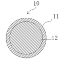
- FIG. 2 is a sectional view of the conductive particles of the present invention (No. 1).
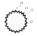
- FIG. 3 is a cross-sectional view of the conductive particles of the present invention (part 2).
- the electroconductive particle of this invention has a core particle and a conductive layer at least, and has a permite
- the core particles are not particularly limited as long as the core particles are formed of at least one of a resin and a metal, and can be appropriately selected depending on the purpose. For example, resin particles, metal particles, and the like Can be mentioned.
- the core particle may have either a single layer structure or a plurality of structures.
- the shape of the resin particle is not particularly limited and may be appropriately selected depending on the intended purpose, but it is preferable that the surface shape has minute irregularities.
- the structure of the resin particles is not particularly limited and may be appropriately selected depending on the intended purpose. Examples thereof include a single layer structure and a laminated structure.
- the number average particle diameter of the resin particles is not particularly limited and may be appropriately selected depending on the intended purpose, but is preferably 1 ⁇ m to 50 ⁇ m, more preferably 2 ⁇ m to 20 ⁇ m, and particularly preferably 5 ⁇ m to 10 ⁇ m.
- the number average particle diameter of the resin particles is less than 1 ⁇ m or exceeds 50 ⁇ m, a product having a sharp particle size distribution may not be obtained, and industrial production is necessary from the viewpoint of practical use. May lack.
- the number average particle diameter of the resin particles is within the particularly preferable range, it is advantageous in that good connection reliability is obtained.
- the number average particle size of the resin particles is measured using, for example, a particle size distribution measuring device (manufactured by Nikkiso Co., Ltd., Microtrac MT3100).
- the material of the resin particles is not particularly limited and can be appropriately selected according to the purpose.
- (meth) acrylic acid ester polymers may be used individually by 1 type and may use 2 or more types together.
- (meth) acrylic acid ester polymers, divinylbenzene polymers, and divinylbenzene polymers are preferable.
- the (meth) acrylic acid ester means either a methacrylic acid ester or an acrylic acid ester
- the (meth) acrylic acid ester is either a crosslinked type or a non-crosslinked type, as required. These may be used in combination.
- the shape of the metal particles is not particularly limited and may be appropriately selected according to the purpose.
- the surface shape may have micro unevenness in that a high current can be passed by increasing the connection area. preferable.
- the structure of the metal particles is not particularly limited and may be appropriately selected depending on the purpose. Examples thereof include a single layer structure and a laminated structure.
- the number average particle diameter of the metal particles is not particularly limited and may be appropriately selected depending on the intended purpose, but is preferably 1 ⁇ m to 50 ⁇ m, more preferably 2 ⁇ m to 20 ⁇ m, and particularly preferably 5 ⁇ m to 10 ⁇ m. If the number average particle diameter of the metal particles is less than 1 ⁇ m or more than 50 ⁇ m, a product with a sharp particle size distribution may not be obtained, and industrial production is necessary from the viewpoint of practical use. May lack. On the other hand, when the number average particle diameter of the metal particles is within the particularly preferable range, it is advantageous in that an indentation inspection can be performed after the connection of PWB and FPC. In addition, the number average particle diameter of the metal particles is measured using, for example, a particle size distribution measuring device (manufactured by Nikkiso Co., Ltd., Microtrac MT3100).
- the material of the metal particles is not particularly limited and can be appropriately selected according to the purpose. Examples thereof include gold, pure nickel, and impurity-containing nickel. There is no restriction
- the conductive layer is not particularly limited as long as it is formed on the surface of the core particle and has a phosphorus-containing hydrophobic group on the surface, and can be appropriately selected according to the purpose.
- a nickel plating layer, nickel / gold plating Examples include layers.
- the plating method for forming the conductive layer is not particularly limited and may be appropriately selected depending on the intended purpose. Examples thereof include an electroless method and a sputtering method.
- the phosphorus-containing hydrophobic group represents a group having a phosphorus atom and a hydrophobic group having 3 or more carbon atoms, and examples thereof include a group represented by the following structural formula (1).
- R represents an alkyl group having 3 or more carbon atoms.
- the hydrophobic group is not particularly limited as long as it has 3 or more carbon atoms, and can be appropriately selected according to the purpose. Examples thereof include an alkyl group (long-chain alkyl chain).
- the alkyl group (long-chain alkyl chain) may have a substituent, may be linear or branched, but a linear one having no substituent is preferable.
- the number of carbon atoms of the alkyl group is not particularly limited as long as it is 3 or more, and can be appropriately selected according to the purpose, but is preferably 3 to 16, and more preferably 4 to 12 .
- the carbon number is less than 3, the surface of the conductive particles may be easily oxidized, and when it exceeds 16, the connection resistance value may be increased.
- the carbon number is within a more preferable range, good connection reliability can be obtained.
- a phosphate group etc. are mentioned.
- Whether or not a phosphorus-containing hydrophobic group is introduced into the conductive layer is determined by either XPS measurement, TOF-SIMS measurement, TEM cross-sectional observation, IR measurement, etc. This can be determined based on the presence or absence of.
- the conductive layer can be prevented from being deteriorated (the hardness of the conductive layer is reduced) and not oxidized, and the surface of the conductive particles can be further prevented from being oxidized.
- the corrosion resistance (moisture resistance) of the conductive particles can be improved.
- the phosphorus concentration in the conductive layer before the hydrophobic treatment with the phosphorus-containing compound is not particularly limited and may be appropriately selected depending on the intended purpose, but is preferably 10% by mass or less, and preferably 2.5% by mass to 7. 0 mass% is more preferable.
- the conductive layer may have a phosphorus concentration gradient. For example, even if the phosphorus concentration on the core particle side of the conductive layer is 15% by mass, the phosphorus concentration in the conductive layer may be 10% by mass or less.
- the conductivity and hardness of the conductive layer increase, and it can be connected to an electrode (wiring) with an oxide film for a long time. Excellent reliability.
- the phosphorus concentration in the conductive layer before the hydrophobization treatment with the phosphorus-containing compound is higher than 10% by mass, the spreadability is increased, so that a low connection resistance cannot be obtained for an electrode (wiring) having an oxide film. There is a case.
- the phosphorus concentration in the conductive layer before the hydrophobization treatment with the phosphorus-containing compound is in a more preferable range, it is advantageous in that good connection reliability can be obtained and the storage stability of the conductive particles can be improved. is there.
- the phosphorus concentration on the surface of the conductive layer that has been hydrophobized with the phosphorus-containing compound is not particularly limited and may be appropriately selected according to the purpose. However, 0.5 mass% to 10 mass% is preferable, and 1 mass% to 8 mass% is more preferable.
- the phosphorus concentration on the surface of the conductive layer is less than 0.5% by mass, the crystallinity of the conductive layer may be too high, and when it exceeds 10% by mass, the conductive layer may be easily oxidized.
- the phosphorus concentration on the surface of the conductive layer is within a more preferable range, it is advantageous in that good connection reliability is obtained.
- the method for adjusting the phosphorus concentration in the conductive layer is not particularly limited and may be appropriately selected depending on the intended purpose.
- the method for controlling the pH of the plating reaction, the phosphoric acid concentration in the plating solution is controlled. Method, etc.
- the method of controlling the pH of the plating reaction is preferable because of excellent reaction control.
- the phosphorus concentration in the conductive layer and the phosphorus concentration on the surface of the conductive layer are measured using, for example, an energy dispersive X-ray analyzer (trade name FAEMAX-7000, manufactured by Horiba, Ltd.).
- the average thickness of the conductive layer is not particularly limited and may be appropriately selected depending on the intended purpose, but is preferably 20 nm to 200 nm, and more preferably 50 nm to 150 nm.
- the connection reliability may be deteriorated.
- the average thickness exceeds 200 nm, the particles tend to aggregate due to plating, and large particles may be easily formed.
- the average thickness of the conductive layer is within a more preferable range, high connection reliability can be obtained, and agglomeration of plating particles can be avoided during the plating step of forming the conductive layer, The formation of two to three plated connecting particles can be prevented, thereby preventing a short circuit.
- the electroconductive particle whose said core particle is a nickel particle can form a nickel plating layer thinly as said electroconductive layer rather than the electroconductive particle whose said core particle is a resin particle.
- the average thickness of the conductive layer is the thickness of the conductive layer of 10 conductive particles selected at random.
- a focused ion beam processing observation apparatus (trade name FB-2100, manufactured by Hitachi High-Technology Corporation) is used. It is a thickness obtained by performing cross-sectional polishing using a transmission electron microscope (trade name H-9500, manufactured by Hitachi High-Technology Corporation) and arithmetically averaging these measured values.
- Examples of the conductive particles 10 include those having nickel particles 12 and a conductive layer 11 formed on the surface of the nickel particles 12 (FIG. 2), those having protrusions 13 (FIG. 3), and the like.
- the method for producing conductive particles of the present invention comprises at least a hydrophobizing treatment step.
- the method for producing conductive particles is a method for producing conductive particles having core particles and a conductive layer formed on the surface of the core particles.
- the core particles are formed of at least one of resin and metal. Examples of the core particles include the core particles exemplified in the description of the conductive particles of the present invention. Examples of the conductive layer include the conductive layer exemplified in the description of the conductive particles of the present invention.
- the hydrophobic treatment step is a step of subjecting the surface of the conductive layer to a hydrophobic treatment with a phosphorus-containing compound.
- the phosphorus-containing compound is not particularly limited as long as it contains phosphorus, and examples thereof include a phosphoric acid compound.
- a phosphoric acid compound There is no restriction
- An alkyl group (long-chain alkyl chain) R is introduced and subjected to a hydrophobic treatment (providing water repellency).
- the number of carbon atoms of the alkyl group (long chain alkyl chain) is not particularly limited and may be appropriately selected depending on the intended purpose, but is preferably 3 to 16, and more preferably 4 to 12. When the carbon number is less than 3, the surface of the conductive particles may be easily oxidized, and when it exceeds 16, the connection resistance value may be increased. On the other hand, when the carbon number is within a more preferable range, good connection reliability can be obtained.
- the hydrophobic treatment is not particularly limited as long as it is a treatment for treating the surface of the conductive layer with a phosphorus-containing compound, and can be appropriately selected depending on the purpose.
- the surface of the conductive layer is hydrophobized with a phosphorus-containing compound, so that only the phosphorus concentration on the surface of the conductive layer is increased while maintaining the phosphorus concentration in the conductive layer low (phosphorus is added to the surface of the conductive layer). Can be unevenly distributed).
- the conductive layer can be deteriorated (the hardness of the conductive layer is lowered) and not oxidized.
- By increasing only the phosphorus concentration on the surface of the conductive layer phosphorus is unevenly distributed on the surface of the conductive layer
- introducing a hydrophobic group in the phosphorus-containing compound into the surface of the conductive particles the corrosion resistance can be improved.
- substitution rate of the phosphate ester compound with respect to all hydroxyl groups on the surface of the conductive layer hydrophobized with the phosphate compound is not particularly limited and can be appropriately selected depending on the purpose.
- the anisotropic conductive film of the present invention includes at least the conductive particles of the present invention and a binder resin, and includes a curing agent, a resin, a silane coupling agent, and other components as necessary.
- the binder resin is not particularly limited as long as it contains at least one of an epoxy resin and an acrylate resin, and can be appropriately selected according to the purpose.
- a thermosetting resin, a photocurable resin, and the like are preferable.
- the binder resin is a thermoplastic resin, the conductive particles cannot be pressed down firmly and connection reliability is deteriorated.
- Specific examples of the binder resin include an epoxy resin and an acrylate resin.
- the epoxy resin is not particularly limited and can be appropriately selected according to the purpose. Examples thereof include bisphenol A type epoxy resins, bisphenol F type epoxy resins, novolac type epoxy resins, modified epoxy resins thereof, and alicyclic epoxy resins. These may be used individually by 1 type and may use 2 or more types together.
- the acrylate resin is not particularly limited and may be appropriately selected depending on the intended purpose.
- the latent hardening agent activated by heating the latent hardening agent which generate
- the latent curing agent activated by heating is not particularly limited and may be appropriately selected depending on the intended purpose. Examples thereof include anionic curing agents such as polyamines and imidazoles and cationic curing agents such as sulfonium salts. Is mentioned.
- ⁇ Resin> As long as it is solid at normal temperature (25 degreeC), there is no restriction
- the content of the resin that is solid at normal temperature is not particularly limited and may be appropriately selected depending on the intended purpose, but is preferably 10% by mass to 80% by mass with respect to the anisotropic conductive film.
- the film property may be insufficient, and a blocking phenomenon may be caused when a reel-shaped product is obtained.
- mass% the tackiness of the film may be lowered and may not be attached to the circuit member.
- the silane coupling agent is not particularly limited and may be appropriately selected depending on the intended purpose. Examples thereof include an epoxy silane coupling agent and an acrylic silane coupling agent. An alkoxysilane derivative is mainly used. Used for.
- the joined body of the present invention includes a first circuit member, a second circuit member facing the first circuit member, and a book disposed between the first circuit member and the second circuit member.
- the electrode of the first circuit member and the electrode of the second circuit member are connected via conductive particles.
- -Second circuit member- There is no restriction
- connection method of the present invention includes at least a film sticking step, an alignment step, and a connection step, and further includes other steps appropriately selected as necessary.
- the said film sticking process is a process of sticking the anisotropic conductive film of this invention to a 1st circuit member or a 2nd circuit member.
- the first circuit member or the second circuit member to which the anisotropic conductive film is attached and the other circuit member to which the anisotropic conductive film is not attached are opposed to terminals (electrodes). ) Is a step of aligning so that they face each other.
- connection step is a step of connecting the electrode in the first circuit member and the electrode in the second circuit member via conductive particles.
- nickel plating process was performed by adding at the speed
- the plating solution is filtered, and the filtrate is washed with pure water, and then dried with a vacuum dryer at 80 ° C., so that a nickel plating layer having a conductive layer phosphorus concentration of 1.3 mass% and an average thickness of 101 nm is obtained.
- the formed nickel plating particles A were produced.
- the thickness of the plating layer was measured by performing cross-sectional polishing on the obtained conductive particles using a focused ion beam processing observation apparatus (trade name FB-2100, manufactured by Hitachi High-Technology Corporation), and a transmission electron microscope (Hitachi High). (Trade name H-9500, manufactured by Technology Co., Ltd.). The results are shown in Table 1.
- Production Example 2 ⁇ Preparation of nickel plating particles B>
- the phosphorous concentration of the conductive layer was set to 2. in the same manner as Production Example 1 except that the mixing ratio of nickel sulfate, sodium hypophosphite, sodium citrate, and thallium nitrate in the mixed solution was changed.
- Nickel-plated particles B on which a nickel-plated layer having 6% by mass and an average thickness of about 101 nm was formed were produced.
- Production Example 3 ⁇ Preparation of nickel plating particles C>
- the phosphorous concentration of the conductive layer was 4.4 in the same manner as in Production Example 1 except that the mixing ratio of nickel sulfate, sodium hypophosphite, sodium citrate, and thallium nitrate in the mixed solution was changed.
- Nickel-plated particles C on which a nickel plating layer having an average thickness of 8 mass% and an average thickness of about 102 nm was formed were produced.
- Production Example 4 ⁇ Preparation of nickel plating particles D>
- the phosphorous concentration of the conductive layer was changed to 6. in the same manner as in Production Example 1 except that the mixing ratio of nickel sulfate, sodium hypophosphite, sodium citrate, and thallium nitrate in the mixed solution was changed.
- Nickel-plated particles D on which a nickel plating layer having an average thickness of 9% by mass and about 100 nm was formed were produced.
- Nickel-plated particles F in which a nickel-plated particle A is plated with gold by a displacement plating method to form a nickel-plated layer having a phosphorous concentration of 0% by mass and an average thickness of 81 nm and a gold-plated layer having a thickness of 20 nm. was made.
- Production Example 7 ⁇ Preparation of nickel plating particles G>
- nickel particles having a mean particle diameter of 5.0 ⁇ m (trade name: Nickel Powder 123, manufactured by Nikko Jamaica Co., Ltd.) were used in the same manner as in Production Example 1 to conduct electricity.
- Examples 1 to 7 ⁇ Preparation of water-repellent particles (hydrophobized particles) A to G> Phosphate ester surfactant (Phosphanol GF-199, manufactured by Toho Chemical Industry Co., Ltd.) is neutralized with potassium hydroxide in an amount that completely neutralizes the acid component, and 10% by mass surfactant An aqueous agent solution was prepared. Into a polypropylene (PP) container, 2.5 g of the prepared 10% by weight surfactant aqueous solution, 50 g of water as a solvent, 50 g of any of nickel plating particles A to E and G and gold plating-nickel particles F were placed. After stirring, drying was performed to produce particles (water-repellent treated particles (hydrophobized particles) A to G) subjected to water-repellent treatment (hydrophobization treatment).
- Phosphate ester surfactant Phosphanol GF-199, manufactured by Toho Chemical Industry Co., Ltd.
- Example 8 ⁇ Preparation of water-repellent treated particles (hydrophobized particles) H>
- a phosphate ester surfactant Phosphanol GF-199, manufactured by Toho Chemical Industry Co., Ltd.
- a phosphate ester surfactant Phosphanol SM-172, Toho Chemical Industry ( A plating layer having a phosphorous concentration of 4.8% by mass and an average thickness of 102 mm in the conductive layer before water repellent treatment (hydrophobization treatment) was formed in the same manner as in Example 3 except that the product was used. Water-repellent treated particles (hydrophobized particles) H were produced.
- bonding materials 1 to 8 (an anisotropic conductive film produced to a thickness of 20 ⁇ m) slit to a width of 1.5 mm are attached to an evaluation IZO coating glass, and an evaluation COF is aligned thereon to temporarily After fixing, under pressure bonding conditions of 190 ° C-4 MPa-10 seconds, pressure bonding is performed using 100 ⁇ m thick Teflon (registered trademark) as a buffer material and a 1.5 mm wide heating tool to produce joined bodies 1-8. did.
- connection resistance ( ⁇ ) when a current of 1 mA was passed was initially measured by a four-terminal method using a digital multimeter (trade name: Digital Multimeter 7555, manufactured by Yokogawa Electric Corporation). And after a reliability test (treatment at a temperature of 85 ° C. and a humidity of 85% for 500 hours). The results are shown in Table 2.
- Example 3 (Comparative Example 3) In Example 3, instead of using a phosphate ester surfactant (Phosphanol GF-199, manufactured by Toho Chemical Industry Co., Ltd.), a silane coupling agent (trade name: A-187, Momentive Performance Materials) In the same manner as in Example 3 except that a silane coupling treatment particle C in which a plating layer having a phosphorous concentration of 4.8% by mass and an average thickness of 102 mm was formed, The joining material 11 and the joined body 11 were obtained, and the electrical conductivity measurement of the particles, the hardness measurement of the particles, the connection resistance measurement of the joined body, the storage stability test, the corrosion evaluation sample preparation, and the corrosion evaluation were performed. The results are shown in Tables 1 and 2.
- Examples 2 to 4 using conductive particles having a phosphorus concentration in the conductive layer before the hydrophobization treatment of 2.6 to 6.9% by mass are shown in Examples 1 and 5 Compared with ⁇ 7, it was found that good results were obtained in electrical conductivity, conduction resistance (after initial and reliability tests), storage stability, and corrosion evaluation.
- the conductive particles of the present invention include a connection between a liquid crystal display and a tape carrier package (Tape Carrier Package: TCP), a connection between a flexible circuit board (Flexible Printed Circuit: FPC) and TCP, or an FPC and a printed wiring board (Printed Wiring). It is suitably used for connection between circuit members such as connection to Board (PWB).
- TCP tape carrier package
- FPC Flexible Printed Circuit
- PWB connection to Board
Landscapes
- Chemical & Material Sciences (AREA)
- Physics & Mathematics (AREA)
- Dispersion Chemistry (AREA)
- Spectroscopy & Molecular Physics (AREA)
- Organic Chemistry (AREA)
- Non-Insulated Conductors (AREA)
- Conductive Materials (AREA)
- Adhesives Or Adhesive Processes (AREA)
Abstract
Description
<1> コア粒子と、該コア粒子の表面に形成された導電層とを有し、前記コア粒子が樹脂及び金属の少なくともいずれかで形成され、前記導電層の表面がリン含有疎水性基を有することを特徴とする導電性粒子である。
<2> コア粒子と、該コア粒子の表面に形成された導電層とを有し、前記コア粒子が樹脂及び金属の少なくともいずれかで形成され、前記導電層の表面がリン含有化合物により疎水化処理されてなることを特徴とする導電性粒子である。
<3> コア粒子が樹脂粒子であり、導電層がニッケルメッキ層である前記<1>から<2>のいずれかに記載の導電性粒子である。
<4> コア粒子と、該コア粒子の表面に形成された導電層とを有する導電性粒子の製造方法であって、前記コア粒子が樹脂及び金属の少なくともいずれかで形成され、前記導電層の表面をリン含有化合物により疎水化処理することを含むことを特徴とする導電性粒子の製造方法である。
<5> リン含有化合物による疎水化処理前の導電層におけるリン濃度が10質量%以下である前記<4>に記載の導電性粒子の製造方法である。
<6> リン含有化合物による疎水化処理前の導電層におけるリン濃度が2.5質量%~7.0質量%である前記<5>に記載の導電性粒子の製造方法である。
<7> リン含有化合物がリン酸化合物である前記<4>から<6>のいずれかに記載の導電性粒子の製造方法である。
<8> 前記<1>から<3>のいずれかに記載の導電性粒子と、バインダー樹脂とを含み、前記バインダー樹脂がエポキシ樹脂及びアクリレート樹脂の少なくともいずれかを含むことを特徴とする異方性導電フィルムである。
<9> フェノキシ樹脂、ポリエステル樹脂、及びウレタン樹脂の少なくともいずれかを更に含む前記<8>に記載の異方性導電フィルムである。
<10> 硬化剤を更に含む前記<8>から<9>のいずれかに記載の異方性導電フィルムである。
<11> シランカップリング剤を更に含む前記<8>から<10>のいずれかに記載の異方性導電フィルムである。
<12> 第1の回路部材と、前記第1の回路部材に対向する第2の回路部材と、前記第1の回路部材及び前記第2の回路部材間に配設された前記<8>から<11>のいずれかに記載の異方性導電フィルムとを有し、前記第1の回路部材における電極と、前記第2の回路部材における電極とが、導電性粒子を介して接続されたことを特徴とする接合体である。
<13> 第1の回路部材がフレキシブル回路基板であり、第2の回路部材がプリント配線基板である前記<12>に記載の接合体である。
<14> 前記<8>から<11>のいずれかに記載の異方性導電フィルムを用いた接続方法であって、第1の回路部材及び第2の回路部材のいずれかに前記異方性導電フィルムを貼付けるフィルム貼付工程と、前記第1の回路部材と前記第2の回路部材とを位置合わせするアライメント工程と、前記第1の回路部材における電極と、前記第2の回路部材における電極とを、導電性粒子を介して接続する接続工程とを含むことを特徴とする接続方法である。
<15> 第1の回路部材がフレキシブル回路基板であり、第2の回路部材がプリント配線基板である前記<14>に記載の接続方法である。
本発明の導電性粒子は、少なくとも、コア粒子と、導電層とを有し、必要に応じて、突起などを有する。
前記コア粒子としては、前記コア粒子が樹脂及び金属の少なくともいずれかで形成されている限り、特に制限はなく、目的に応じて適宜選択することができ、例えば、樹脂粒子、金属粒子、などが挙げられる。前記コア粒子は、単層構造、複数構造のいずれであってもよい。
前記樹脂粒子としては、特に制限はなく、目的に応じて適宜選択することができる。
前記樹脂粒子の数平均粒子径が1μm未満であり、又は、50μmを超えると、粒度分布がシャープなものが得られないことがあり、工業的な製造が実用的用途の点からみても必要性に欠けることがある。一方、前記樹脂粒子の数平均粒子径が前記特に好ましい範囲内であると、良好な接続信頼性を得る点で有利である。
なお、前記樹脂粒子の数平均粒子径は、例えば、粒度分布測定装置(日機装社製、マイクロトラックMT3100)を用いて測定される。
これらの中でも、(メタ)アクリル酸エステル重合体、ジビニルベンゼン重合体、ジビニルベンゼン系重合体が好ましい。
ここで、(メタ)アクリル酸エステルとは、メタクリル酸エステル及びアクリル酸エステルのいずれかを意味し、前記(メタ)アクリル酸エステルは、必要に応じて、架橋型、非架橋型いずれかであってもよく、これらを混合して用いてもよい。
前記金属粒子としては、特に制限はなく、目的に応じて適宜選択することができる。
前記金属粒子の数平均粒子径が1μm未満であり、又は、50μmを超えると、粒度分布がシャープなものが得られないことがあり、工業的な製造が実用的用途の点からみても必要性に欠けることがある。一方、前記金属粒子の数平均粒子径が、前記特に好ましい範囲内であると、PWBとFPCとの接続後に圧痕検査が可能となる点で有利である。
なお、前記金属粒子の数平均粒子径は、例えば、粒度分布測定装置(日機装社製、マイクロトラックMT3100)を用いて測定される。
前記導電層としては、コア粒子の表面に形成され、表面にリン含有疎水性基を有する限り、特に制限はなく、目的に応じて適宜選択することができ、例えば、ニッケルメッキ層、ニッケル/金メッキ層などが挙げられる。
前記リン含有疎水性基は、リン原子及び炭素数3以上の疎水性基を有する基を表し、例えば、下記構造式(1)で表される基が挙げられる。

前記疎水性基としては、炭素数3以上である限り、特に制限はなく、目的に応じて適宜選択することができ、例えば、アルキル基(長鎖アルキル鎖)、などが挙げられる。なお、前記アルキル基(長鎖アルキル鎖)は、置換基を有していてもよく、直鎖状でも、分岐を有していてもよいが、置換基を有さない直鎖状のものが好ましい。
前記アルキル基(長鎖アルキル鎖)の炭素数としては、3以上である限り、特に制限はなく、目的に応じて適宜選択することができるが、3~16が好ましく、4~12がより好ましい。
前記炭素数が3未満であると、導電性粒子の表面が酸化し易くなることがあり、16を超えると、接続抵抗値が高くなることがある。一方、前記炭素数がより好ましい範囲内であると、良好な接続信頼性を得ることができる。
前記リン含有疎水性基の具体例としては、特に制限はなく、目的に応じて適宜選択することができ、例えば、リン酸エステル基、などが挙げられる。
前記導電層にリン含有疎水性基が導入されたか否かは、XPSによる測定、TOF-SIMSによる測定、TEMによる断面観察、IR測定、などにより、導電層表面におけるリン原子及びエステル結合のいずれかの存在の有無により、判断することができる。
そこで、前記導電層の表面にリン含有疎水性基を導入して、導電層におけるリン濃度を低く維持し、導電層の表面のリン濃度のみを高くする (導電層の表面にリンを偏在させる)ことにより、導電層が劣化して(導電層の硬度が低下して)酸化しないようにすることができ、また、導電性粒子の表面が酸化するのを更に防止することができ、さらに、導電性粒子の耐腐食性(耐湿性)を向上させることができる。
ここで、前記導電層内でリン濃度勾配を有していてもよい。例えば、前記導電層のコア粒子側のリン濃度が15質量%であっても、前記導電層におけるリン濃度が10質量%以下であればよい。
前記リン含有化合物による疎水化処理前の導電層におけるリン濃度が10質量%以下であると、導電層の導電率及び硬度が高くなり、酸化膜のある電極(配線)に対しても長期にわたり接続信頼性が優れる。一方、前記リン含有化合物による疎水化処理前の導電層におけるリン濃度が10質量%より高くなると、延展性が増すことで、酸化膜のある電極(配線)に対して低い接続抵抗が得られない場合がある。一方、前記リン含有化合物による疎水化処理前の導電層におけるリン濃度がより好ましい範囲内であると、良好な接続信頼性を得る点や導電性粒子の保存安定性の向上ができる点で有利である。
前記導電層表面のリン濃度が0.5質量%未満であると、導電層の結晶性が高くなり過ぎることがあり、10質量%を超えると、導電層が酸化し易くなることがある。一方、前記導電層表面のリン濃度が、より好ましい範囲内であると、良好な接続信頼性を得る点で有利である。
これらの中でも、メッキ反応のpHを制御する方法が、反応制御に優れている点で、好ましい。
なお、前記導電層におけるリン濃度及び前記導電層表面のリン濃度は、例えば、エネルギー分散型X線分析装置(堀場製作所製、商品名FAEMAX-7000)を用いて測定される。
前記導電層の平均厚みが20nm未満であると、接続信頼性が悪化することがあり、200nmを超えると、粒子同士がメッキにより凝集しやすくなり、巨大粒子ができ易くなることがある。一方、前記導電層の平均厚みが、より好ましい範囲内であると、高い接続信頼性を得ることができ、また、導電層を形成するメッキ工程時に、メッキ粒子の凝集を回避することができ、2個~3個のメッキ連結粒子が形成されるのを防止して、ショートを防止することができる。
また、前記コア粒子がニッケル粒子である導電性粒子は、前記コア粒子が樹脂粒子である導電性粒子よりも、前記導電層としてニッケルメッキ層を薄く形成することができる。
なお、前記導電層の平均厚みは、無作為に選んだ10個の導電性粒子の導電層の厚みを、例えば、収束イオンビーム加工観察装置(日立ハイテクノロジー社製、商品名FB-2100)を用いて断面研磨を行い、透過電子顕微鏡(日立ハイテクノロジー社製、商品名H-9500)を用いて測定し、これらの測定値を算術平均した厚みである。
本発明の導電性粒子の製造方法は、少なくとも、疎水化処理工程を含んでなる。
前記導電性粒子の製造方法は、コア粒子と、該コア粒子の表面に形成された導電層とを有する導電性粒子の製造方法である。
前記コア粒子は、樹脂及び金属の少なくともいずれかで形成されている。
前記コア粒子としては、例えば、本発明の前記導電性粒子の説明において例示した前記コア粒子などが挙げられる。
前記導電層としては、例えば、本発明の前記導電性粒子の説明において例示した前記導電層などが挙げられる。
前記疎水化処理工程は、導電層の表面をリン含有化合物により疎水化処理する工程である。
前記リン含有化合物としては、リンを含有する限り、特に制限はなく、例えば、リン酸化合物、などが挙げられる。
前記リン酸化合物としては、特に制限はなく、目的に応じて適宜選択することができ、例えば、末端に水酸基及びアルキル基を有する界面活性剤、などが挙げられる。
前記界面活性剤は、例えば、図1に示すように、末端の水酸基と、ニッケルメッキ粒子100の表面の水酸基における水素原子とが脱離する脱水縮合反応が起こって、ニッケルメッキ粒子100の表面にアルキル基(長鎖アルキル鎖)Rが導入され、疎水化処理(撥水性が付与)される。
前記アルキル基(長鎖アルキル鎖)の炭素数としては、特に制限はなく、目的に応じて適宜選択することができるが、3~16が好ましく、4~12がより好ましい。
前記炭素数が3未満であると、導電性粒子の表面が酸化し易くなることがあり、16を超えると、接続抵抗値が高くなることがある。一方、前記炭素数がより好ましい範囲内であると、良好な接続信頼性を得ることができる。
前記疎水化処理としては、リン含有化合物で導電層の表面を処理する処理である限り、特に制限はなく、目的に応じて適宜選択することができる。
本発明の異方性導電フィルムは、本発明の導電性粒子と、バインダー樹脂とを少なくとも含み、硬化剤、樹脂、シランカップリング剤、必要に応じて、その他の成分を含む。
前記バインダー樹脂としては、エポキシ樹脂及びアクリレート樹脂の少なくともいずれかを含む限り、特に制限はなく、目的に応じて適宜選択することができるが、熱硬化性樹脂、光硬化性樹脂、などが好ましい。なお、前記バインダー樹脂が熱可塑性樹脂である場合、導電性粒子をしっかりと押さえ込むことができずに接続信頼性が悪化してしまう。
前記バインダー樹脂の具体例としては、エポキシ樹脂、アクリレート樹脂、などが挙げられる。
前記エポキシ樹脂としては、特に制限はなく、目的に応じて適宜選択することができ、
例えば、ビスフェノールA型エポキシ樹脂、ビスフェノールF型エポキシ樹脂、ノボラッ
ク型エポキシ樹脂、それらの変性エポキシ樹脂、脂環式エポキシ樹脂などが挙げられる。これらは、1種単独で使用してもよいし、2種以上を併用してもよい。
前記アクリレート樹脂としては、特に制限はなく、目的に応じて適宜選択することができ、例えば、メチルアクリレート、エチルアクリレート、イソプロピルアクリレート、イソブチルアクリレート、エポキシアクリレート、エチレングリコールジアクリレート、ジエチレングリコールジアクリレート、トリメチロールプロパントリアクリレート、ジメチロールトリシクロデカンジアクリレート、テトラメチレングリコールテトラアクリレート、2-ヒドロキシ-1,3-ジアクリロキシプロパン、2,2-ビス[4-(アクリロキシメトキシ)フェニル]プロパン、2,2-ビス[4-(アクリロキシエトキシ)フェニル]プロパン、ジシクロペンテニルアクリレート、トリシクロデカニルアクリレート、トリス(アクリロキシエチル)イソシアヌレート、ウレタンアクリレートなどが挙げられる。これらは、1種単独で使用してもよいし、2種以上を併用してもよい。
また、前記アクリレートをメタクリレートにしたものが挙げられ、これらは、1種単独で使用してもよいし、2種以上を併用してもよい。
前記硬化剤としては、特に制限はなく、目的に応じて適宜選択することができ、例えば、加熱により活性化する潜在性硬化剤、加熱により遊離ラジカルを発生させる潜在性硬化剤などが挙げられる。
前記加熱により活性化する潜在性硬化剤としては、特に制限はなく、目的に応じて適宜選択することができ、例えば、ポリアミン、イミダゾール等のアニオン系硬化剤やスルホニウム塩などのカチオン系硬化剤などが挙げられる。
前記加熱により遊離ラジカルを発生させる潜在性硬化剤としては、特に制限はなく、目的に応じて適宜選択することができ、例えば、有機過酸化物やアゾ化合物などが挙げられる。
前記樹脂としては、常温(25℃)で固形である限り、特に制限はなく、目的に応じて適宜選択することができ、例えば、フェノキシ樹脂、ポリエステル樹脂、及びウレタン樹脂などが挙げられる。前記ポリエステル樹脂としては、特に制限はなく、目的に応じて適宜選択することができ、飽和ポリエステル樹脂、不飽和ポリエステル樹脂のいずれであってもよい。
前記常温で固形である樹脂の含有量としては、特に制限はなく、目的に応じて適宜選択することができるが、異方性導電フィルムに対して10質量%~80質量%が好ましい。
前記常温で固形である樹脂の含有量が、異方性導電フィルムに対して10質量%未満であると、膜性に欠け、リール状の製品にしたときにブロッキング現象を引き起こすことがあり、80質量%を超えると、フィルムのタックが低下して回路部材に貼り付かなくなることがある。
前記シランカップリング剤としては、特に制限はなく、目的に応じて適宜選択することができ、例えば、エポキシ系シランカップリング剤、アクリル系シランカップリング剤、などが挙げられ、アルコキシシラン誘導体が主に用いられる。
本発明の接合体は、第1の回路部材と、前記第1の回路部材に対向する第2の回路部材と、前記第1の回路部材及び前記第2の回路部材間に配設された本発明の異方性導電フィルムとを有し、前記第1の回路部材における電極と、前記第2の回路部材における電極とが、導電性粒子を介して接続されている。
前記第1の回路部材としては、特に制限はなく、目的に応じて適宜選択することができ、例えば、FPC基板、PWB基板などが挙げられる。これらの中でも、FPC基板が好ましい。
前記第2の回路部材としては、特に制限はなく、目的に応じて適宜選択することができ、例えば、FPC基板、COF(chip on film)基板、TCP基板、PWB基板、IC基板、パネルなどが挙げられる。これらの中でも、PWB基板が好ましい。
本発明の接続方法は、フィルム貼付工程と、アライメント工程と、接続工程とを少なくとも含み、更に必要に応じて適宜選択した、その他の工程を含む。
前記フィルム貼付工程は、第1の回路部材又は第2の回路部材に、本発明の異方性導電フィルムを貼付ける工程である。
前記アライメント工程は、異方性導電フィルムが貼付けられた第1の回路部材又は第2の回路部材と、異方性導電フィルムが貼付けられていないもう一方の回路部材とを、相対する端子(電極)同士が対向するように、位置合わせする工程である。
前記接続工程は、第1の回路部材における電極と、第2の回路部材における電極とを、導電性粒子を介して接続する工程である。
前記その他の工程としては、特に制限はなく、目的に応じて適宜選択することができる。
<ニッケルメッキ粒子Aの作製>
数平均粒子径3.8μmのスチレン樹脂粒子(積水化学工業社製、商品名:ミクロパール)を、硝酸タリウム水溶液に投入し、60℃に加温させた状態で攪拌しながら、アンモニア水又は硫酸で所定のpHに調整した、硫酸ニッケル(アルドリッチ社製)、次亜リン酸ナトリウム(アルドリッチ社製)、クエン酸ナトリウム(アルドリッチ社製)、硝酸タリウム(アルドリッチ社製)の混合溶液を30mL/分の速度で添加することでニッケルメッキ処理を行った。そのメッキ液をろ過し、ろ過物を純水で洗浄した後、80℃の真空乾燥機で乾燥させることにより、導電層のリン濃度が1.3質量%、平均厚みが101nmのニッケルメッキ層が形成されたニッケルメッキ粒子Aを作製した。
なお、前記メッキ層の厚み測定は、得られた導電性粒子を収束イオンビーム加工観察装置(日立ハイテクノロジー社製、商品名FB-2100)を用いて断面研磨を行い、透過電子顕微鏡(日立ハイテクノロジー社製、商品名H-9500)を用いて行った。結果を表1に示す。
<ニッケルメッキ粒子Bの作製>
製造例1において、混合溶液中の硫酸ニッケル、次亜リン酸ナトリウム、クエン酸ナトリウム、硝酸タリウムの混合比を変更したこと以外は、製造例1と同様にして、導電層のリン濃度が2.6質量%、平均厚みが約101nmのニッケルメッキ層が形成されたニッケルメッキ粒子Bを作製した。
<ニッケルメッキ粒子Cの作製>
製造例1において、混合溶液中の硫酸ニッケル、次亜リン酸ナトリウム、クエン酸ナトリウム、硝酸タリウムの混合比を変更したこと以外は、製造例1と同様にして、導電層のリン濃度が4.8質量%、平均厚みが約102nmのニッケルメッキ層が形成されたニッケルメッキ粒子Cを作製した。
<ニッケルメッキ粒子Dの作製>
製造例1において、混合溶液中の硫酸ニッケル、次亜リン酸ナトリウム、クエン酸ナトリウム、硝酸タリウムの混合比を変更したこと以外は、製造例1と同様にして、導電層のリン濃度が6.9質量%、平均厚みが約100nmのニッケルメッキ層が形成されたニッケルメッキ粒子Dを作製した。
<ニッケルメッキ粒子Eの作製>
製造例1において、混合溶液中の硫酸ニッケル、次亜リン酸ナトリウム、クエン酸ナトリウム、硝酸タリウムの混合比を変更したこと以外は、製造例1と同様にして、導電層のリン濃度が9.8質量%、平均厚みが約102nmのニッケルメッキ層が形成されたニッケルメッキ粒子Eを作製した。
<ニッケル金メッキ粒子Fの作製>
ニッケルメッキ粒子Aを置換メッキ法により表面に金メッキを施すことで、導電層のリン濃度が0質量%、平均厚みが81nmのニッケルメッキ層及び厚みが20nmの金メッキ層が形成されたニッケル金メッキ粒子Fを作製した。
<ニッケルメッキ粒子Gの作製>
製造例1において、スチレン樹脂粒子を用いる代わりに、平均粒子径5.0μmのニッケル粒子(日興リカ社製、商品名ニッケルパウダー123)を用いたこと以外は、製造例1と同様にして、導電層のリン濃度が5.0質量%、平均厚みが101mmのメッキ層が形成された金メッキ-ニッケル粒子Gを作製した。
<撥水処理粒子(疎水化処理粒子)A~Gの作製>
リン酸エステル系界面活性剤(フォスファノールGF-199、東邦化学工業(株)製)を、その酸成分が完全に中和される量の水酸化カリウムにより中和し、10質量%界面活性剤水溶液を作製した。この作製した10質量%界面活性剤水溶液2.5g、溶媒である水50g、ニッケルメッキ粒子A~E、G及び金メッキ-ニッケル粒子Fのいずれかの粒子50gを、ポリプロピレン(PP)容器に入れ、攪拌後、乾燥を行い、撥水性処理(疎水化処理)を施した粒子(撥水処理粒子(疎水化処理粒子)A~G)を作製した。
<撥水処理粒子(疎水化処理粒子)Hの作製>
実施例3において、リン酸エステル界面活性剤(フォスファノールGF-199、東邦化学工業(株)製)を用いる代わりに、リン酸エステル界面活性剤(フォスファノールSM-172、東邦化学工業(株)製)を用いたこと以外は、実施例3と同様にして、撥水処理(疎水化処理)前の導電層のリン濃度が4.8質量%、平均厚みが102mmのメッキ層が形成された撥水処理粒子(疎水化処理粒子)Hを作製した。
作製された撥水処理粒子(疎水化処理粒子)A~Hについて、下記測定方法で電気伝導度の測定を行った。
-電気伝導度の測定方法-
60℃の純水中で洗浄及び乾燥を行ったポリプロピレン(PP)容器を用いて、導電性粒子0.4gに対して200mLの超純水を入れ、100℃10時間で抽出を行った。その後、1時間冷却し、濾紙にてろ過を行った抽出液を、電気伝導度測定器(東亜DKK製、商品名:CM-31P)にて、電気伝導度の測定を行った。結果を表2に示す。
前記リン濃度測定は、前記エネルギー分散型X線分析装置(堀場製作所製、商品名FAEMAX-7000)を用いて行った。結果を表1に示す。
下記組成の接着剤中に、撥水処理粒子(疎水化処理粒子)A~Hのいずれかの粒子を粒子密度が10,000個/mm2となるように分散させ、斯かる接着剤を、シリコン処理された剥離PETフィルム上に塗布し、乾燥させることにより厚み20μmの接合材料1~8を得た。
フェノキシ樹脂(巴工業社製、商品名:PKHC) 50質量部
ラジカル重合性樹脂(ダイセル・サイテック社製、商品名:EB-600)
45質量部
シランカップリング剤(信越シリコーン社製、商品名:KBM-503) 2質量部
疎水性シリカ(EVONIK社製、AEROSIL972) 3質量部
反応開始剤(日本油脂社製、商品名:パーヘキサC) 3質量部
得られた接合材料1~8(20μm厚に作製した異方性導電フィルム)を用いて、評価用COF(50μmピッチ(Line/Space=1/1)、Cu8μm厚-Snメッキ、38μm厚-S’perflex基材)と、評価用IZOコーティングガラス(全表面IZOコーティングガラス、基材厚み0.7mm)との接続を行った。まず、1.5mm幅にスリットされた接合材料1~8(20μm厚に作製した異方性導電フィルム)を評価用IZOコーティングガラスに貼り付け、その上に、評価用COFを位置合わせして仮固定した後、190℃-4MPa-10秒間の圧着条件で、緩衝材としての100μm厚のテフロン(登録商標)及び1.5mm幅の加熱ツールを用いて圧着を行い、接合体1~8を作製した。
作製した接合体1~8について、デジタルマルチメータ(商品名:デジタルマルチメータ7555、横河電機社製)を用いて4端子法により、電流1mAを流したときの接続抵抗(Ω)を、初期と信頼性試験(温度85℃、湿度85%で500時間処理)後について測定した。結果を表2に示す。
作製された撥水処理粒子(疎水化処理粒子)A~Hについて、30℃/60%環境オーブンに48時間と投入して、エージングを行ったのち、接合材料1~8を作製し、さらに、接合体1~8を作製し、作製した接合体1~8の接続抵抗を測定した。結果を表2に示す。
評価基材として、評価用櫛歯パターンガラス(Line/Space=25/13、ITO配線)を接続材料で覆い、190℃-4MPa-10秒間の圧着条件で、緩衝材としての100μm厚のテフロン(登録商標)及び1.5mm幅の加熱ツールを用いて圧着を行い、腐食評価サンプルを作製した。
作製した腐食評価サンプルを60℃湿度95%の環境中にて暴露し、15Vの直流電圧を50時間印加し、ITO配線の腐食発生の有無を確認した。評価結果を表2に示す。
実施例1~8において、撥水処理粒子(疎水化処理粒子)A~Hのいずれかの粒子を用いる代わりに、ニッケルメッキ粒子A、G及び金メッキ-ニッケル粒子Fを用いたこと以外は、実施例1~8と同様にして、接合材料9、10及び12及び接合体9、10及び12を得て、粒子の電気伝導度の測定、粒子の硬度測定、接合体の接続抵抗測定、保存安定性試験、腐食評価サンプル作製、及び腐食評価を行った。結果を表1及び表2に示す。
実施例3において、リン酸エステル界面活性剤(フォスファノールGF-199、東邦化学工業(株)製)を用いる代わりに、シランカップリング剤(商品名:A-187、モメンティブ・パフォーマンス・マテリアルズ社製)を用いたこと以外は、実施例3同様にして、導電層のリン濃度が4.8質量%、平均厚みが102mmのメッキ層が形成されたシランカップリング処理粒子Cを作製し、接合材料11及び接合体11を得て、粒子の電気伝導度の測定、粒子の硬度測定、接合体の接続抵抗測定、保存安定性試験、腐食評価サンプル作製、及び腐食評価を行った。結果を表1及び表2に示す。

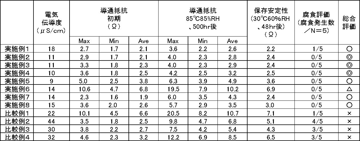
また、表1及び表2より、疎水化処理前の導電層におけるリン濃度が2.6質量%~6.9質量%の導電性粒子を用いた実施例2~4が、実施例1及び5~7と比較して、電気伝導度、導通抵抗(初期及び信頼性試験後)、保存安定性、腐食評価において、良好な結果が得られたことが分かった。
11 導電層
12 ニッケル粒子
13 突起
100 ニッケルメッキ粒子
Claims (14)
- コア粒子と、該コア粒子の表面に形成された導電層とを有し、
前記コア粒子が樹脂及び金属の少なくともいずれかで形成され、
前記導電層の表面がリン含有疎水性基を有することを特徴とする導電性粒子。 - コア粒子が樹脂粒子であり、導電層がニッケルメッキ層である請求項1に記載の導電性粒子。
- コア粒子と、該コア粒子の表面に形成された導電層とを有する導電性粒子の製造方法であって、
前記コア粒子が樹脂及び金属の少なくともいずれかで形成され、
前記導電層の表面をリン含有化合物により疎水化処理することを含むことを特徴とする導電性粒子の製造方法。 - リン含有化合物による疎水化処理前の導電層におけるリン濃度が10質量%以下である請求項3に記載の導電性粒子の製造方法。
- リン含有化合物による疎水化処理前の導電層におけるリン濃度が2.5質量%~7.0質量%である請求項4に記載の導電性粒子の製造方法。
- リン含有化合物がリン酸化合物である請求項3から5のいずれかに記載の導電性粒子の製造方法。
- 請求項1から2のいずれかに記載の導電性粒子と、バインダー樹脂とを含み、前記バインダー樹脂がエポキシ樹脂及びアクリレート樹脂の少なくともいずれかを含むことを特徴とする異方性導電フィルム。
- フェノキシ樹脂、ポリエステル樹脂、及びウレタン樹脂の少なくともいずれかを更に含む請求項7に記載の異方性導電フィルム。
- 硬化剤を更に含む請求項7から8のいずれかに記載の異方性導電フィルム。
- シランカップリング剤を更に含む請求項7から9のいずれかに記載の異方性導電フィルム。
- 第1の回路部材と、前記第1の回路部材に対向する第2の回路部材と、前記第1の回路部材及び前記第2の回路部材間に配設された請求項7から10のいずれかに記載の異方性導電フィルムとを有し、前記第1の回路部材における電極と、前記第2の回路部材における電極とが、導電性粒子を介して接続されたことを特徴とする接合体。
- 第1の回路部材がフレキシブル回路基板であり、第2の回路部材がプリント配線基板である請求項11に記載の接合体。
- 請求項7から10のいずれかに記載の異方性導電フィルムを用いた接続方法であって、第1の回路部材及び第2の回路部材のいずれかに前記異方性導電フィルムを貼付けるフィルム貼付工程と、前記第1の回路部材と前記第2の回路部材とを位置合わせするアライメント工程と、前記第1の回路部材における電極と、前記第2の回路部材における電極とを、導電性粒子を介して接続する接続工程とを含むことを特徴とする接続方法。
- 第1の回路部材がフレキシブル回路基板であり、第2の回路部材がプリント配線基板である請求項13に記載の接続方法。
Priority Applications (4)
| Application Number | Priority Date | Filing Date | Title |
|---|---|---|---|
| HK13101646.1A HK1174433B (en) | 2010-08-31 | 2011-08-23 | Conductive particle, method for producing same, anisotropic conductive film, assembly and connection method |
| KR1020127018144A KR101385330B1 (ko) | 2010-08-31 | 2011-08-23 | 도전성 입자 및 그 제조 방법, 및 이방성 도전 필름, 접합체 및 접속 방법 |
| CN201180013160.4A CN102792386B (zh) | 2010-08-31 | 2011-08-23 | 导电性粒子及其制造方法以及各向异性导电膜、接合体及连接方法 |
| US13/552,858 US8987607B2 (en) | 2010-08-31 | 2012-07-19 | Conductive particle, and anisotropic conductive film, bonded structure, and bonding method |
Applications Claiming Priority (2)
| Application Number | Priority Date | Filing Date | Title |
|---|---|---|---|
| JP2010193790A JP5410387B2 (ja) | 2010-08-31 | 2010-08-31 | 導電性粒子及びその製造方法、並びに異方性導電フィルム、接合体、及び接続方法 |
| JP2010-193790 | 2010-08-31 |
Related Child Applications (1)
| Application Number | Title | Priority Date | Filing Date |
|---|---|---|---|
| US13/552,858 Continuation US8987607B2 (en) | 2010-08-31 | 2012-07-19 | Conductive particle, and anisotropic conductive film, bonded structure, and bonding method |
Publications (1)
| Publication Number | Publication Date |
|---|---|
| WO2012029587A1 true WO2012029587A1 (ja) | 2012-03-08 |
Family
ID=43424760
Family Applications (1)
| Application Number | Title | Priority Date | Filing Date |
|---|---|---|---|
| PCT/JP2011/068915 Ceased WO2012029587A1 (ja) | 2010-08-31 | 2011-08-23 | 導電性粒子及びその製造方法、並びに異方性導電フィルム、接合体、及び接続方法 |
Country Status (6)
| Country | Link |
|---|---|
| US (1) | US8987607B2 (ja) |
| JP (1) | JP5410387B2 (ja) |
| KR (1) | KR101385330B1 (ja) |
| CN (1) | CN102792386B (ja) |
| TW (1) | TWI443684B (ja) |
| WO (1) | WO2012029587A1 (ja) |
Cited By (1)
| Publication number | Priority date | Publication date | Assignee | Title |
|---|---|---|---|---|
| JP2014011117A (ja) * | 2012-07-02 | 2014-01-20 | Nippon Shokubai Co Ltd | 導電性微粒子 |
Families Citing this family (15)
| Publication number | Priority date | Publication date | Assignee | Title |
|---|---|---|---|---|
| GB201018379D0 (en) * | 2010-10-29 | 2010-12-15 | Conpart As | Conductive rf particles |
| GB201018380D0 (en) | 2010-10-29 | 2010-12-15 | Conpart As | Process |
| JP5629641B2 (ja) * | 2011-05-19 | 2014-11-26 | 株式会社日本触媒 | 導電性微粒子及びその製造方法 |
| JP6084868B2 (ja) * | 2012-03-09 | 2017-02-22 | 積水化学工業株式会社 | 導電性粒子、導電材料及び接続構造体 |
| JP6357347B2 (ja) * | 2013-05-14 | 2018-07-11 | 積水化学工業株式会社 | 導電性粒子、導電材料及び接続構造体 |
| JP6453032B2 (ja) * | 2013-10-21 | 2019-01-16 | 積水化学工業株式会社 | 導電性粒子、導電材料及び接続構造体 |
| JP6429228B2 (ja) * | 2014-04-24 | 2018-11-28 | タツタ電線株式会社 | 金属被覆樹脂粒子及びそれを用いた導電性接着剤 |
| JP6443732B2 (ja) * | 2014-10-24 | 2018-12-26 | 日立金属株式会社 | 導電性粒子、導電性粉体、導電性高分子組成物および異方性導電シート |
| FR3042305B1 (fr) * | 2015-10-13 | 2019-07-26 | Arkema France | Procede de fabrication d'un materiau composite conducteur et materiau composite ainsi obtenu |
| CN114221146B (zh) * | 2016-11-30 | 2024-11-22 | 迪睿合株式会社 | 导电粒子配置膜、其制造方法、检查探头单元、导通检查方法 |
| WO2018181546A1 (ja) * | 2017-03-29 | 2018-10-04 | 日立化成株式会社 | 導電粒子の選別方法、回路接続材料、接続構造体及びその製造方法、並びに導電粒子 |
| CN110473654B (zh) * | 2019-06-11 | 2021-08-06 | 惠科股份有限公司 | 一种导电粒子及其制备方法和一种显示面板 |
| KR20230011946A (ko) | 2020-05-20 | 2023-01-25 | 니폰 가가쿠 고교 가부시키가이샤 | 도전성 입자, 그것을 사용한 도전성 재료 및 접속 구조체 |
| CN114725161A (zh) | 2020-12-22 | 2022-07-08 | 三星显示有限公司 | 包括各向异性导电膜的显示装置和制造显示装置的方法 |
| CN118213103A (zh) * | 2024-04-28 | 2024-06-18 | 安徽华晟新能源科技股份有限公司 | 导电材料、光伏焊带和光伏组件 |
Citations (5)
| Publication number | Priority date | Publication date | Assignee | Title |
|---|---|---|---|---|
| JPH05258790A (ja) * | 1992-03-13 | 1993-10-08 | Nitto Denko Corp | 異方導電性接着フィルムおよびこれを用いた接続構造 |
| JP2008222785A (ja) * | 2007-03-09 | 2008-09-25 | Asahi Kasei Electronics Co Ltd | 異方導電性接着フィルム |
| JP2009029862A (ja) * | 2007-07-25 | 2009-02-12 | Asahi Kasei Electronics Co Ltd | 異方性導電フィルム |
| JP2010086664A (ja) * | 2008-09-29 | 2010-04-15 | Sekisui Chem Co Ltd | 導電性微粒子、異方性導電材料、及び、接続構造体 |
| JP2010103080A (ja) * | 2008-03-27 | 2010-05-06 | Sekisui Chem Co Ltd | 導電性微粒子、異方性導電材料、及び、接続構造体 |
Family Cites Families (13)
| Publication number | Priority date | Publication date | Assignee | Title |
|---|---|---|---|---|
| EP0560072A3 (en) | 1992-03-13 | 1993-10-06 | Nitto Denko Corporation | Anisotropic electrically conductive adhesive film and connection structure using the same |
| JP2004109943A (ja) * | 2002-09-20 | 2004-04-08 | Ricoh Co Ltd | 画像形成装置 |
| JP3847693B2 (ja) * | 2002-09-30 | 2006-11-22 | シャープ株式会社 | 半導体装置の製造方法 |
| KR101131229B1 (ko) | 2004-01-30 | 2012-03-28 | 세키스이가가쿠 고교가부시키가이샤 | 도전성 미립자 및 이방성 도전 재료 |
| WO2006025485A1 (ja) | 2004-09-02 | 2006-03-09 | Sekisui Chemical Co., Ltd. | 導電性微粒子及び異方性導電材料 |
| JP4860163B2 (ja) | 2005-02-15 | 2012-01-25 | 積水化学工業株式会社 | 導電性微粒子の製造方法 |
| JP4936678B2 (ja) * | 2005-04-21 | 2012-05-23 | 積水化学工業株式会社 | 導電性粒子及び異方性導電材料 |
| KR100790856B1 (ko) * | 2005-07-15 | 2008-01-03 | 삼성전기주식회사 | 인산계 분산제를 포함하는 적층 세라믹 콘덴서 |
| JP5529431B2 (ja) | 2008-03-27 | 2014-06-25 | 積水化学工業株式会社 | 導電性微粒子、異方性導電材料、及び、接続構造体 |
| JP5549069B2 (ja) | 2008-04-22 | 2014-07-16 | 日立化成株式会社 | 異方性導電接着剤用粒子状導電材料及びその製造方法、並びに異方性導電接着剤 |
| JP2010003682A (ja) * | 2008-05-21 | 2010-01-07 | Canon Inc | 有機発光装置の製造方法 |
| JP5151902B2 (ja) * | 2008-10-21 | 2013-02-27 | 住友電気工業株式会社 | 異方導電性フィルム |
| JP5358328B2 (ja) | 2009-07-16 | 2013-12-04 | デクセリアルズ株式会社 | 導電性粒子、並びに異方性導電フィルム、接合体、及び接続方法 |
-
2010
- 2010-08-31 JP JP2010193790A patent/JP5410387B2/ja active Active
-
2011
- 2011-08-23 WO PCT/JP2011/068915 patent/WO2012029587A1/ja not_active Ceased
- 2011-08-23 CN CN201180013160.4A patent/CN102792386B/zh active Active
- 2011-08-23 KR KR1020127018144A patent/KR101385330B1/ko active Active
- 2011-08-30 TW TW100131112A patent/TWI443684B/zh active
-
2012
- 2012-07-19 US US13/552,858 patent/US8987607B2/en active Active
Patent Citations (5)
| Publication number | Priority date | Publication date | Assignee | Title |
|---|---|---|---|---|
| JPH05258790A (ja) * | 1992-03-13 | 1993-10-08 | Nitto Denko Corp | 異方導電性接着フィルムおよびこれを用いた接続構造 |
| JP2008222785A (ja) * | 2007-03-09 | 2008-09-25 | Asahi Kasei Electronics Co Ltd | 異方導電性接着フィルム |
| JP2009029862A (ja) * | 2007-07-25 | 2009-02-12 | Asahi Kasei Electronics Co Ltd | 異方性導電フィルム |
| JP2010103080A (ja) * | 2008-03-27 | 2010-05-06 | Sekisui Chem Co Ltd | 導電性微粒子、異方性導電材料、及び、接続構造体 |
| JP2010086664A (ja) * | 2008-09-29 | 2010-04-15 | Sekisui Chem Co Ltd | 導電性微粒子、異方性導電材料、及び、接続構造体 |
Cited By (1)
| Publication number | Priority date | Publication date | Assignee | Title |
|---|---|---|---|---|
| JP2014011117A (ja) * | 2012-07-02 | 2014-01-20 | Nippon Shokubai Co Ltd | 導電性微粒子 |
Also Published As
| Publication number | Publication date |
|---|---|
| CN102792386B (zh) | 2015-11-25 |
| TWI443684B (zh) | 2014-07-01 |
| US8987607B2 (en) | 2015-03-24 |
| US20120279781A1 (en) | 2012-11-08 |
| TW201214472A (en) | 2012-04-01 |
| KR20120094123A (ko) | 2012-08-23 |
| JP2010278026A (ja) | 2010-12-09 |
| KR101385330B1 (ko) | 2014-04-14 |
| CN102792386A (zh) | 2012-11-21 |
| JP5410387B2 (ja) | 2014-02-05 |
| HK1174433A1 (zh) | 2013-06-07 |
Similar Documents
| Publication | Publication Date | Title |
|---|---|---|
| JP5410387B2 (ja) | 導電性粒子及びその製造方法、並びに異方性導電フィルム、接合体、及び接続方法 | |
| KR101748454B1 (ko) | 도전성 입자, 이방성 도전 필름, 접합체 및 접속 방법 | |
| JP4930623B2 (ja) | 回路接続材料、これを用いたフィルム状回路接続材料、回路部材の接続構造及び回路部材の接続方法 | |
| KR102467618B1 (ko) | 접착제 조성물 | |
| KR101856816B1 (ko) | 이방성 도전 필름, 이방성 도전 필름의 제조 방법, 접속 방법 및 접합체 | |
| KR20210022541A (ko) | 도전성 입자, 도전 재료 및 접속 구조체 | |
| JP2024160304A (ja) | 接着剤フィルム | |
| JP2013251099A (ja) | 導電粒子及びその製造方法 | |
| JP5796232B2 (ja) | 導電性粒子、異方性導電材料及び接続構造体 | |
| HK1174433B (en) | Conductive particle, method for producing same, anisotropic conductive film, assembly and connection method |
Legal Events
| Date | Code | Title | Description |
|---|---|---|---|
| WWE | Wipo information: entry into national phase |
Ref document number: 201180013160.4 Country of ref document: CN |
|
| 121 | Ep: the epo has been informed by wipo that ep was designated in this application |
Ref document number: 11821604 Country of ref document: EP Kind code of ref document: A1 |
|
| ENP | Entry into the national phase |
Ref document number: 20127018144 Country of ref document: KR Kind code of ref document: A |
|
| NENP | Non-entry into the national phase |
Ref country code: DE |
|
| 122 | Ep: pct application non-entry in european phase |
Ref document number: 11821604 Country of ref document: EP Kind code of ref document: A1 |