WO2012023458A1 - 照明装置、表示装置及びテレビ受信装置 - Google Patents
照明装置、表示装置及びテレビ受信装置 Download PDFInfo
- Publication number
- WO2012023458A1 WO2012023458A1 PCT/JP2011/068132 JP2011068132W WO2012023458A1 WO 2012023458 A1 WO2012023458 A1 WO 2012023458A1 JP 2011068132 W JP2011068132 W JP 2011068132W WO 2012023458 A1 WO2012023458 A1 WO 2012023458A1
- Authority
- WO
- WIPO (PCT)
- Prior art keywords
- hole
- chassis
- support pin
- rivet
- substrate
- Prior art date
- Legal status (The legal status is an assumption and is not a legal conclusion. Google has not performed a legal analysis and makes no representation as to the accuracy of the status listed.)
- Ceased
Links
Images








Classifications
-
- F—MECHANICAL ENGINEERING; LIGHTING; HEATING; WEAPONS; BLASTING
- F21—LIGHTING
- F21V—FUNCTIONAL FEATURES OR DETAILS OF LIGHTING DEVICES OR SYSTEMS THEREOF; STRUCTURAL COMBINATIONS OF LIGHTING DEVICES WITH OTHER ARTICLES, NOT OTHERWISE PROVIDED FOR
- F21V21/00—Supporting, suspending, or attaching arrangements for lighting devices; Hand grips
-
- G—PHYSICS
- G02—OPTICS
- G02F—OPTICAL DEVICES OR ARRANGEMENTS FOR THE CONTROL OF LIGHT BY MODIFICATION OF THE OPTICAL PROPERTIES OF THE MEDIA OF THE ELEMENTS INVOLVED THEREIN; NON-LINEAR OPTICS; FREQUENCY-CHANGING OF LIGHT; OPTICAL LOGIC ELEMENTS; OPTICAL ANALOGUE/DIGITAL CONVERTERS
- G02F1/00—Devices or arrangements for the control of the intensity, colour, phase, polarisation or direction of light arriving from an independent light source, e.g. switching, gating or modulating; Non-linear optics
- G02F1/01—Devices or arrangements for the control of the intensity, colour, phase, polarisation or direction of light arriving from an independent light source, e.g. switching, gating or modulating; Non-linear optics for the control of the intensity, phase, polarisation or colour
- G02F1/13—Devices or arrangements for the control of the intensity, colour, phase, polarisation or direction of light arriving from an independent light source, e.g. switching, gating or modulating; Non-linear optics for the control of the intensity, phase, polarisation or colour based on liquid crystals, e.g. single liquid crystal display cells
- G02F1/133—Constructional arrangements; Operation of liquid crystal cells; Circuit arrangements
- G02F1/1333—Constructional arrangements; Manufacturing methods
- G02F1/1335—Structural association of cells with optical devices, e.g. polarisers or reflectors
- G02F1/1336—Illuminating devices
- G02F1/133602—Direct backlight
- G02F1/133603—Direct backlight with LEDs
-
- G—PHYSICS
- G02—OPTICS
- G02F—OPTICAL DEVICES OR ARRANGEMENTS FOR THE CONTROL OF LIGHT BY MODIFICATION OF THE OPTICAL PROPERTIES OF THE MEDIA OF THE ELEMENTS INVOLVED THEREIN; NON-LINEAR OPTICS; FREQUENCY-CHANGING OF LIGHT; OPTICAL LOGIC ELEMENTS; OPTICAL ANALOGUE/DIGITAL CONVERTERS
- G02F1/00—Devices or arrangements for the control of the intensity, colour, phase, polarisation or direction of light arriving from an independent light source, e.g. switching, gating or modulating; Non-linear optics
- G02F1/01—Devices or arrangements for the control of the intensity, colour, phase, polarisation or direction of light arriving from an independent light source, e.g. switching, gating or modulating; Non-linear optics for the control of the intensity, phase, polarisation or colour
- G02F1/13—Devices or arrangements for the control of the intensity, colour, phase, polarisation or direction of light arriving from an independent light source, e.g. switching, gating or modulating; Non-linear optics for the control of the intensity, phase, polarisation or colour based on liquid crystals, e.g. single liquid crystal display cells
- G02F1/133—Constructional arrangements; Operation of liquid crystal cells; Circuit arrangements
- G02F1/1333—Constructional arrangements; Manufacturing methods
- G02F1/1335—Structural association of cells with optical devices, e.g. polarisers or reflectors
- G02F1/1336—Illuminating devices
- G02F1/133602—Direct backlight
- G02F1/133605—Direct backlight including specially adapted reflectors
-
- G—PHYSICS
- G02—OPTICS
- G02F—OPTICAL DEVICES OR ARRANGEMENTS FOR THE CONTROL OF LIGHT BY MODIFICATION OF THE OPTICAL PROPERTIES OF THE MEDIA OF THE ELEMENTS INVOLVED THEREIN; NON-LINEAR OPTICS; FREQUENCY-CHANGING OF LIGHT; OPTICAL LOGIC ELEMENTS; OPTICAL ANALOGUE/DIGITAL CONVERTERS
- G02F1/00—Devices or arrangements for the control of the intensity, colour, phase, polarisation or direction of light arriving from an independent light source, e.g. switching, gating or modulating; Non-linear optics
- G02F1/01—Devices or arrangements for the control of the intensity, colour, phase, polarisation or direction of light arriving from an independent light source, e.g. switching, gating or modulating; Non-linear optics for the control of the intensity, phase, polarisation or colour
- G02F1/13—Devices or arrangements for the control of the intensity, colour, phase, polarisation or direction of light arriving from an independent light source, e.g. switching, gating or modulating; Non-linear optics for the control of the intensity, phase, polarisation or colour based on liquid crystals, e.g. single liquid crystal display cells
- G02F1/133—Constructional arrangements; Operation of liquid crystal cells; Circuit arrangements
- G02F1/1333—Constructional arrangements; Manufacturing methods
- G02F1/1335—Structural association of cells with optical devices, e.g. polarisers or reflectors
- G02F1/1336—Illuminating devices
- G02F1/133602—Direct backlight
- G02F1/133608—Direct backlight including particular frames or supporting means
-
- G—PHYSICS
- G02—OPTICS
- G02F—OPTICAL DEVICES OR ARRANGEMENTS FOR THE CONTROL OF LIGHT BY MODIFICATION OF THE OPTICAL PROPERTIES OF THE MEDIA OF THE ELEMENTS INVOLVED THEREIN; NON-LINEAR OPTICS; FREQUENCY-CHANGING OF LIGHT; OPTICAL LOGIC ELEMENTS; OPTICAL ANALOGUE/DIGITAL CONVERTERS
- G02F1/00—Devices or arrangements for the control of the intensity, colour, phase, polarisation or direction of light arriving from an independent light source, e.g. switching, gating or modulating; Non-linear optics
- G02F1/01—Devices or arrangements for the control of the intensity, colour, phase, polarisation or direction of light arriving from an independent light source, e.g. switching, gating or modulating; Non-linear optics for the control of the intensity, phase, polarisation or colour
- G02F1/13—Devices or arrangements for the control of the intensity, colour, phase, polarisation or direction of light arriving from an independent light source, e.g. switching, gating or modulating; Non-linear optics for the control of the intensity, phase, polarisation or colour based on liquid crystals, e.g. single liquid crystal display cells
- G02F1/133—Constructional arrangements; Operation of liquid crystal cells; Circuit arrangements
- G02F1/1333—Constructional arrangements; Manufacturing methods
- G02F1/1335—Structural association of cells with optical devices, e.g. polarisers or reflectors
- G02F1/1336—Illuminating devices
- G02F1/133602—Direct backlight
- G02F1/133609—Direct backlight including means for improving the color mixing, e.g. white
-
- H—ELECTRICITY
- H04—ELECTRIC COMMUNICATION TECHNIQUE
- H04N—PICTORIAL COMMUNICATION, e.g. TELEVISION
- H04N3/00—Scanning details of television systems; Combination thereof with generation of supply voltages
- H04N3/10—Scanning details of television systems; Combination thereof with generation of supply voltages by means not exclusively optical-mechanical
- H04N3/14—Scanning details of television systems; Combination thereof with generation of supply voltages by means not exclusively optical-mechanical by means of electrically scanned solid-state devices
Definitions
- the present invention relates to a lighting device, a display device, and a television receiver.
- image display devices such as television receivers are shifting from conventional cathode ray tubes to thin display devices to which thin display elements such as liquid crystal panels and plasma display panels are applied.
- liquid crystal panel When a liquid crystal panel is used as the display element, the liquid crystal panel does not emit light, and thus a backlight device is separately required as a lighting device.
- a light source block attached to a back chassis, a diffused light guide plate, a reflection sheet that reflects illumination light toward the diffused light guide plate, and attached to the back chassis, the tip is diffused.
- a transmissive type comprising a plurality of optical stud members abutted against the light guide plate, each defining a facing distance between the diffused light guiding plate and the reflecting sheet and a facing distance between the reflecting sheet and the back chassis.
- a backlight device is disclosed.
- the optical stud member (support pin) can suppress the diffusion light guide plate (optical member) from being bent toward the back chassis, and the diffusion light guide plate can be positioned with high accuracy in the backlight device. It is said that the occurrence of uneven brightness can be prevented.
- the reflective sheet may be locked to the chassis together with the substrate (light source block) by rivets so that the reflective sheet does not float.
- the support pins and the rivets are fixed to the chassis via the reflection sheet and the substrate, and the reflection sheet and the substrate are provided with through holes through which the support pins and the rivets are inserted. Yes.
- the support pin through-hole and the rivet through-hole provided in the reflective sheet are identified and attached at a predetermined position, but the support pin through-hole and the rivet through-hole are attached.
- the support pin and the rivet may be attached by mistake. If the rivet is mistakenly attached to the through hole for the support pin, the optical member cannot be supported, and the optical member cannot be positioned with high accuracy in the backlight device, resulting in uneven brightness. There is a fear.
- the present invention has been completed based on the above circumstances, and suppresses erroneous mounting of the support pin and the rivet in the lighting device including the support pin for supporting the optical member and the rivet for locking the reflection sheet. And it aims at providing the illuminating device which can suppress generation
- an illumination device of the present invention includes a light source, a substrate on which the light source is mounted on one surface side, a chassis that supports the other surface side of the substrate, and the one surface side of the substrate.
- a reflection sheet disposed; an optical member that diffuses light facing the reflection sheet; a first through hole and a second through hole provided in the reflection sheet; and a substrate side through hole provided in the substrate. And attached to the chassis via the first through hole and the substrate side through hole, and attached to the chassis via the support pin for supporting the optical member, the second through hole and the substrate side through hole.
- a rivet for fixing the reflective sheet and the substrate to the chassis, and the reflective sheet is formed adjacent to or close to either the first through hole or the second through hole, 1st An opening for identifying a hole and the second through-hole, and at least one of the surfaces of the substrate is provided in a range overlapping with the opening, and the reflection sheet is different in color, and the reflection sheet And a colored portion that can be distinguished from the above.
- a colored portion that can be distinguished from the reflective sheet is provided in a range overlapping with the opening on one surface of the substrate.
- the support pin and the rivet are attached, a part of the colored portion is visually recognized from the opening, so that it is easy to determine the presence or absence of the opening, and the first through hole provided in the reflection sheet and the first through hole are provided.
- the two through holes can be easily identified.
- the apparatus further comprises a flange formed on the support pin and a head smaller than the flange formed on the rivet, and the opening is formed adjacent to or close to the first through hole.
- the opening is hidden in the flange portion, while the rivet is disposed in the first through hole and the substrate.
- at least a part of the opening can be visually recognized.
- the apparatus further comprises a flange formed on the support pin and a head larger than the flange formed on the rivet, and the opening is adjacent to or close to the second through hole.
- the opening is hidden in the head, while the support pin is attached to the second through hole and the board side through hole.
- at least a part of the opening can be visually recognized.
- the colored portion may be provided in a range overlapping with the opening, the first through hole, and the second through hole.
- the said structure WHEREIN It further attaches to the said chassis via the said board
- the periphery of the hole may have a color that can be distinguished from the colored portion.
- the board side through hole through which the temporary fixing member is inserted and the board side through hole through which the support pin and the rivet are inserted can be identified by the presence or absence of the colored portion. It is possible to prevent the stop member from being erroneously inserted into the substrate side through hole through which the support pin and the rivet are inserted.
- the colored portion may be formed by printing on the substrate. With such a configuration, the colored portion can be easily formed.
- the colored portion may be provided only in a range overlapping with the opening, the first through hole, and the second through hole on the one surface of the substrate.
- the colored portion is not provided except in a range overlapping with the opening, the first through hole, and the second through hole. For this reason, the consumption of the printing ink used for formation of a coloring part can be suppressed, and it can contribute to cost reduction.
- a display device of the present invention includes the above-described illumination device and a display panel that performs display using light from the illumination device.
- a liquid crystal panel can be exemplified as the display panel.
- Such a display device can be applied as a liquid crystal display device to various uses, for example, a desktop screen of a television or a personal computer, and is particularly suitable for a large screen.
- a television receiver includes the display device.
- FIG. 2 is an exploded perspective view illustrating a schematic configuration of the television receiver according to the first embodiment.
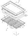
- the disassembled perspective view which shows schematic structure of the liquid crystal display device with which the television receiver of FIG. 1 is provided.
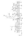
- Sectional drawing which shows the cross-sectional structure along the long side direction of the liquid crystal display device of FIG.
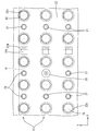
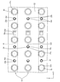
- FIG. 3 is an enlarged plan view in which the periphery of a support pin according to Embodiment 1 is enlarged.
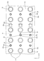
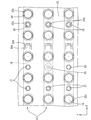
- FIG. 10 is an enlarged plan view in which support pins, rivets, and a reflection sheet according to Embodiment 5 are omitted.
- FIGS. 1 A first embodiment of the present invention will be described with reference to FIGS.
- the liquid crystal display device 10 is illustrated.
- the X axis, the Y axis, and the Z axis are drawn in a part of each drawing, and the drawing is such that each axis direction is a common direction in each drawing.
- the upper side shown in FIG. 3 be a front side, and let the lower side of the figure be a back side.
- the television receiver TV includes a liquid crystal display device 10, front and back cabinets Ca and Cb that are accommodated so as to sandwich the liquid crystal display device 10, a power source P, a tuner T, And a stand S.
- the liquid crystal display device 10 (display device) has a horizontally long rectangular shape (rectangular shape) as a whole, and is accommodated in a vertically placed state.
- the liquid crystal display device 10 includes a liquid crystal panel 11 that is a display panel and a backlight device 12 (illumination device) that is an external light source, which are integrated by a frame-like bezel 13 or the like. Is supposed to be retained.
- the screen size is 42 inches and the aspect ratio is 16: 9.
- the liquid crystal panel 11 (display panel) has a rectangular shape in plan view, and a pair of glass substrates are bonded together with a predetermined gap therebetween, and liquid crystal is sealed between the glass substrates. It is said.
- One glass substrate is provided with a switching element (for example, TFT) connected to a source wiring and a gate wiring orthogonal to each other, a pixel electrode connected to the switching element, an alignment film, and the like.
- the substrate is provided with a color filter and counter electrodes in which colored portions such as R (red), G (green), and B (blue) are arranged in a predetermined arrangement, and an alignment film.
- polarizing plates 11A and 11B are disposed on the outer sides of both glass substrates.
- the backlight device 12 is a so-called direct-type backlight device in which a plurality of LED units U are provided directly below the back surface of the panel surface (display surface) of the liquid crystal panel 11.
- the backlight device 12 includes a chassis 14 having a substantially box shape opened on the light emitting surface side (the liquid crystal panel 11 side), and an optical member 15 arranged so as to cover the opening of the chassis 14.
- a group (diffusing plate 15a and a plurality of optical sheets 15b disposed between the diffusing plate 15a and the liquid crystal panel 11), the outer edge of the optical member 15 group disposed along the outer edge of the chassis 14 and the chassis 14 A frame 16 that is sandwiched and held, and a chassis reflection sheet 22 that covers almost the entire inner surface of the chassis 14 and reflects the light in the chassis 14 toward the optical member 15 side.
- LED units U light source units
- LEDs 17 Light Emitting Diodes
- a support pin 20 for holding, and a rivet 21 for holding the chassis reflection sheet 22 and the LED board 18 are provided.
- the optical member 15 side (front side) from the LED unit U is the light emitting side.
- the chassis 14 is made of metal, and as shown in FIGS. 2 and 3, a bottom plate 14a having a rectangular shape like the liquid crystal panel 11, a side plate 14b rising from an outer end of each side of the bottom plate 14a, and a side plate 14b It consists of a receiving plate 14c projecting outward from the rising end, and as a whole has a shallow substantially box shape (substantially shallow dish shape) opened toward the front side.
- the long side direction of the chassis 14 coincides with the X-axis direction (horizontal direction), and the short side direction coincides with the Y-axis direction (vertical direction).
- a frame 16 and an optical member 15 to be described later can be placed on each receiving plate 14c in the chassis 14 from the front side.
- a frame 16 is screwed to each receiving plate 14c.
- support pin mounting holes 14 d are opened at positions corresponding to the installation positions of the support pins 20
- rivet mounting holes 14 e are opened at positions corresponding to the installation positions of the rivets 21.
- the optical member 15 has a horizontally long rectangular shape (rectangular shape) in a plan view, like the liquid crystal panel 11 and the chassis 14. As shown in FIG. 3, the optical member 15 covers the opening of the chassis 14 by placing the outer edge portion of the optical member 15 on the receiving plate 14 c, and is disposed between the liquid crystal panel 11 and the LED unit U. .
- the optical member 15 includes a diffusion plate 15a disposed on the back side (the LED unit U side, the side opposite to the light emitting side) and an optical sheet 15b disposed on the front side (the liquid crystal panel 11 side, the light emitting side). Is done.
- the diffusing plate 15a has a structure in which a large number of diffusing particles are dispersed in a substantially transparent resin base material having a predetermined thickness, and has a function of diffusing transmitted light.
- the optical sheet 15b has a sheet shape that is thinner than the diffusion plate 15a. Specific types of the optical sheet 15b include, for example, a diffusion sheet, a lens sheet, a reflective polarizing sheet, and the like, which can be appropriately selected and used.
- the frame 16 has a frame shape along the outer peripheral edge portions of the liquid crystal panel 11 and the optical member 15. As shown in FIG. 3, an outer edge portion of the optical member 15 can be sandwiched between the frame 16 and each receiving plate 14c.
- the frame 16 can receive the outer edge of the liquid crystal panel 11 from the back side.
- a bezel 13 is screwed to the front side of the frame 16. Thereby, the outer edge portion of the liquid crystal panel 11 can be sandwiched between the bezel 13 and the frame 16.
- the LED unit U (light source unit) will be described in detail.
- the LED units U have a shape that is long in the X-axis direction, and a plurality of sets (9 sets in this embodiment) are arranged along the Y-axis direction.
- the LED unit U is mainly composed of an LED 17 (light source) and an LED substrate 18 (substrate) on which the LED 17 is mounted. Further, the LED unit U is provided with a diffusing lens 19 attached to a position corresponding to the LED 17 on the LED substrate 18.
- the constituent parts of the LED unit U will be sequentially described in detail.
- the LED 17 is a kind of point light source that has a point shape when seen in a plan view, and a plurality (17 in this embodiment) of LEDs 17 are arranged along the long side direction (X-axis direction) of the LED substrate 18.
- the LED 17 has a configuration in which an LED chip is sealed with a resin material on a substrate portion fixed to the LED substrate 18.
- the LED chip mounted on the substrate unit has one main emission wavelength, and specifically, one that emits blue light in a single color is used.
- a phosphor that converts blue light emitted from the LED chip into white light is dispersed and blended in the resin material for sealing the LED chip. As a result, the LED 17 can emit white light.
- the LED 17 is a so-called top type in which the surface opposite to the mounting surface with respect to the LED substrate 18 (surface facing the front side) is the light emitting surface 17a.
- the optical axis E1 of the LED 17 is set to substantially coincide with the Z-axis direction (direction orthogonal to the main plate surfaces of the liquid crystal panel 11 and the optical member 15).
- the light emitted from the LED 17 spreads radially to some extent within a predetermined angle range around the optical axis E1, but its directivity is higher than that of a cold cathode tube or the like. . That is, the emission intensity of the LED 17 shows an angular distribution that tends to decrease as the direction along the optical axis E1 is high and the tilt angle with respect to the optical axis E1 increases.
- the LED substrate 18 has a rectangular shape that is long in the X-axis direction in a plan view, and the long-side direction matches the X-axis direction, and the short-side direction matches the Y-axis direction.
- the chassis 14 is accommodated while extending along the bottom plate 14a. That is, the LED 17 is disposed on the bottom plate 14a of the chassis.
- the connector part 18a is provided in the both ends of the long side direction in the LED board 18. As shown in FIG.
- the front side surface of the LED board 18 is composed of a board reflection sheet 18b.
- the board reflection sheet 18b is made of, for example, a synthetic resin and has a white surface with excellent light reflectivity.
- the board reflection sheet 18b is arranged so as to overlap with the lens holes 22c formed in the chassis reflection sheet 22.
- the light incident on the region corresponding to the lens hole 22c can be reflected toward the diffusion lens 19 side.
- the light utilization efficiency can be increased, and the luminance can be improved. In other words, sufficient brightness can be obtained even when the number of LEDs 17 is reduced to reduce the cost.
- the LED board 18 is provided with support pin insertion holes 18c (substrate side through holes) at positions corresponding to positions where the support pins 20 are installed, and rivet insertion holes 18d at positions corresponding to positions where the rivets 21 are installed. (Substrate side through hole) is established.
- a coloring portion 24 that surrounds the support pin insertion hole 18c and the rivet insertion hole 18d and colors the LED substrate 18.
- the coloring portion 24 has a circular shape in plan view, and among the front-side surface of the LED substrate 18, an identification opening portion 23 provided on a later-described chassis reflection sheet 22 and a support pin hole. In the range which overlaps with 22a and the rivet hole 22b, it forms by screen printing using a black coating material.
- the coloring part 24 and the chassis reflection sheet 22 have different colors and can be distinguished by visual observation. For this reason, when attaching the support pin 20 and the rivet 21, a part of the colored portion 24 is visually observed through the opening 23, the support pin hole 22a, and the rivet hole 22b provided in the chassis reflection sheet 22. Thus, the visibility of the opening 23, the support pin hole 22a, and the rivet hole 22b can be improved.
- the diffusion lens 19 is made of a synthetic resin material (for example, polycarbonate, acrylic, etc.) that is substantially transparent (having high translucency) and has a refractive index higher than that of air.
- the diffusing lens 19 has a lens body 19a having a predetermined thickness and having a substantially circular shape when viewed in a plane, and covers each LED 17 individually from the front side with respect to the LED substrate 18, that is, viewed in a plane. Are attached so as to overlap each LED 17.
- a protrusion 19e is provided on the periphery of the lower surface 19b of the diffusing lens 19.
- the projections 19e are arranged at three locations at substantially equal intervals (approximately 120 ° intervals) along the peripheral edge of the diffusing lens 19 in plan view, and are fixed to the LED substrate 18 with, for example, an adhesive or a thermosetting resin. ing.
- a portion that overlaps with the LED 17 in plan view is formed with a substantially conical incident recess 19d that is recessed upward. Light from the LED 17 is incident on 19d.
- the lower surface of the diffusing lens 19 is subjected to a surface roughening process such as a graining process.
- the diffusing lens 19 On the other hand, on the upper surface of the diffusing lens 19 (the surface facing the diffusing plate 15a), a concave portion 19f that is depressed downward is formed in the central portion (a portion overlapping the LED 17 in plan view), and two gentle arcs are formed. A continuous emission surface 19c is formed.
- the light emitted from the LED 17 is diffused in a planar shape by being refracted between the air layer and the incident recess 19d and between the emission surface 19c and the air layer, and is diffused from the emission surface 19c to the diffusion plate 15a over a wide angle range. Irradiated to the side. In this way, the diffuser lens 19 can emit light having a strong directivity emitted from the light emitting surface 17a of the LED 17 while diffusing.
- the region of the light emitting surface 19c that overlaps with the LED 17 when viewed in a plane is a region where the amount of light from the LED 17 is extremely larger than other regions, and the brightness is locally increased. Therefore, by forming the concave portion 19f described above at the center of the upper surface of the diffusing lens 19, most of the light from the LED 17 is emitted while being refracted at a wide angle, or part of the light from the LED 17 is on the LED substrate 18 side. Can be reflected. Thereby, it can suppress that the brightness
- the LED units U composed of the above-described components are arranged in parallel in the chassis 14 in a state where the long side direction and the short side direction are aligned with each other in the X-axis direction and the Y-axis direction.
- the LED unit U (LED board 18) has a row direction in the X-axis direction (the long side direction of the chassis 14 and the LED board 18) in the chassis 14, and the Y-axis direction (the short side of the chassis 14 and the LED board 18).
- (Direction) is the column direction (arranged in a matrix).
- a plurality of LEDs 17 are arranged in a matrix in the X-axis direction and the Y-axis direction (the direction along the chassis bottom plate 14a).
- a total of 27 LED units U are arranged in parallel in the chassis 14, three in the X-axis direction and nine in the Y-axis direction.
- two types of LED boards 18 forming the LED unit U having different long side dimensions and the number of mounted LEDs 17 are used.
- the LED substrate 18 six LEDs 17 are mounted, and the long side dimension is a relatively long six-part mounting type and the five LEDs 17 are mounted, and the long side dimension is relatively long.
- the short five-mount type is used, one for the six-mount type at the X-axis direction end position of the chassis 14 and one for the five-mount type at the central position in the same direction. , Each is arranged.
- the LED boards 18 that form one row along the X-axis direction are electrically connected to each other by fitting and connecting the adjacent connector portions 18a to each other.
- Connector portions 18a corresponding to both ends in the X-axis direction are electrically connected to external control circuits (not shown).
- the LEDs 17 arranged on the LED boards 18 in one row are connected in series, and the lighting / extinction of a large number of LEDs 17 included in the row is collectively controlled by a single control circuit. Therefore, it is possible to reduce the cost.
- the short side dimension and the arrangement pitch of LED17 are made substantially the same.
- each liquid crystal display device 10 having a screen size of, for example, 26 inches, 32 inches, 37 inches, 40 inches, 42 inches, 46 inches, 52 inches, and 65 inches is used. Therefore, it is possible to easily cope with the manufacture at a low cost.
- a chassis reflection sheet 22 is laminated on the front surface of each LED board 18 described above.
- the chassis reflection sheet 22 and the LED board 18 are supported by support pins 20 and rivets 21 on the bottom plate of the chassis. 14a is fixed. Furthermore, the support pin 20 can support the optical member 15 from below.
- the chassis reflective sheet 22 (reflective sheet) is set to a size that covers almost the entire inner surface of the chassis 14, and is made of, for example, a synthetic resin, and the surface exhibits a white color with excellent light reflectivity. Is done.
- the bottom portion of the chassis reflection sheet 22 has a substantially rectangular shape in plan view, and a support pin hole 22 a, that is, a first through hole is formed at a position corresponding to the position where the support pin 20 is installed.
- a rivet hole 22b that is, a second through hole is formed at a location corresponding to the position where the rivet 21 is installed.
- the support pin hole 22 a (first through hole) has a circular shape when seen in a plan view, and its diameter is larger than the diameter of the support pin insertion hole 18 c provided in the LED substrate 18. Is also set larger.
- the rivet hole 22b (second through hole) has a circular shape when seen in a plan view, and the diameter thereof is set larger than the diameter of the rivet insertion hole 18d provided in the LED board 18. Further, an opening 23 is provided adjacent to the support pin hole 22a.
- the opening 23 has a substantially oval shape in plan view, and is formed at a position adjacent to the support pin hole 22a by an opening continuous from the circular support pin hole 22a.
- the size of the opening 23 is such that when the support pin 20 described later is attached to the chassis 14 via the support pin hole 20a and the support pin insertion hole 18c, the opening 23 is hidden by the flange 20b of the support pin.
- the rivet 21 is attached to the chassis 14 via the support pin hole 22a and the support pin insertion hole 18c, at least a part of the opening 23 is visually recognized.
- a lens hole 22c is opened at a position corresponding to the diffusing lens 19 provided in the LED unit U, and a connector hole 22d is opened at a position corresponding to the connector portion 18a at the bottom of the chassis reflection sheet 22.
- the lens hole 22 c has a circular shape when seen in a plan view, and its diameter is set larger than the diameter of the diffusing lens 19.
- the connector hole 22d has a rectangular shape when seen in a plan view and is set larger than the connector portion 18a.
- the support pin 20 is located near the center of the bottom plate 14a of the chassis.
- the support pin 20 is made of a synthetic resin and has a white surface with excellent light reflectivity.
- the support pin 20 extends from the upper surface of the chassis reflection sheet 22 to the front side (Z-axis direction), and a columnar portion 20a that restricts the deflection of the optical member 15 by contacting the tip of the optical member 15 and the columnar portion 20a.
- a flange portion 20b extending toward the outer side in the horizontal direction from the peripheral edge side of the base end, and protruding from the flange portion 20b along the direction opposite to the columnar portion 20a, into the support pin insertion hole 18c and the support pin mounting hole 14d.
- an attachment portion 20c that is inserted and fixed to the chassis 14.
- the columnar portion 20a has a substantially conical shape, and when the diffusion plate 15a is bent downward, the diffusion plate 15a and the tip of the columnar portion 20a are in point contact with each other, so that the diffusion plate 15a is viewed from below. Support is possible. For this reason, it becomes possible to suppress that the optical member 15 bends to the chassis 14 side, the optical member 15 can be positioned in the backlight apparatus 12 with high precision, and it can suppress that a brightness nonuniformity arises.
- the flange portion 20b has a substantially disk shape, is larger than the diameter of the support pin hole 22a of the chassis reflection sheet, and covers the support pin hole 22a and the opening 23 for identification in an attached state. Further, the flange portion 20b and the chassis reflection sheet 22 are opposed to each other with a slight gap so that the lifting of the chassis reflection sheet 22 with respect to the LED substrate 18 can be suppressed.
- the attachment portion 20c is a wide portion whose tip can be elastically deformed, and is inserted into the support pin hole 22a, the support pin insertion hole 18c, and the support pin attachment hole 14d, and is fixed to the chassis 14.
- the LED board 18 has a support pin insertion hole 18c through which the mounting portion 20c is inserted, and the chassis bottom plate 14a has a hole. Is provided with a support pin mounting hole 14d communicating with the support pin insertion hole 18c, and the mounting portion 20c is inserted through the support pin mounting hole 14c and can be locked to the rear surface side of the chassis bottom plate 14a.
- the rivet 21 is arranged on the bottom plate 14a of the chassis along the LED board 18, and is made of, for example, a synthetic resin, and has a white surface with excellent light reflectivity. Is done.
- the rivet 21 includes a disc-shaped head 21a larger than the rivet hole 22b provided in the chassis reflection sheet 22, and a mounting portion 21b protruding downward from the center of the head 21a.
- the head portion 21a has a substantially disc shape and is configured to cover the rivet hole 22b in an attached state, which is larger than the diameter of the rivet hole 22b of the chassis reflection sheet. Further, the head 21a and the chassis reflection sheet 22 are opposed to each other with a slight gap, and the lifting of the chassis reflection sheet 22 with respect to the LED substrate 18 can be suppressed. Further, the diameter of the head 21a is smaller than the diameter of the flange 20b of the support pin. When the rivet 21 is mistakenly attached to the support pin hole 22a, at least one of the identification opening 23 is provided. The part is visible.
- the attachment portion 21b is a wide portion whose tip can be elastically deformed, and is inserted into the rivet hole 22b, the rivet insertion hole 18d, and the rivet attachment hole 14e, and is fixed to the LED substrate 18 and the chassis 14.
- the LED board 18 is provided with a rivet insertion hole 18d for inserting the attachment portion 21b
- the bottom plate 14a of the chassis includes A rivet attachment hole 14e communicating with the rivet insertion hole 18d is formed, and the attachment portion 21b can be inserted through the rivet insertion hole 18d and locked to the back side of the chassis bottom plate 14a.
- the LED boards 18 are arranged at predetermined positions on the bottom plate 14a of the chassis, and the LED boards 18 adjacent in the horizontal direction are connected to each other. It connects by the part 18a.
- the positions of the support pin insertion holes 18c of the LED board and the support pin mounting holes 14d of the chassis are aligned, and the positions of the rivet insertion holes 18d of the LED board and the rivet mounting holes 14e of the chassis are aligned.
- the LED 17 is mounted on the LED substrate 18 and a diffusion lens 19 is attached.
- the chassis reflection sheet 22 is placed oppositely on the front surface of each LED board 18.
- the diffusing lens 19 passes through the lens hole 22c of the chassis reflection sheet, and the connector portion 18a passes through the connector hole 22d of the chassis reflection sheet.
- the identification opening 23 of the chassis reflection sheet 22 overlaps with the colored portion 24 of the LED substrate 18, and a part of the colored portion 24 can be visually observed through the opening 23.
- the positions of the support pin holes 22a of the chassis reflection sheet and the support pin insertion holes 18c of the LED board are aligned, and the LED board 18 is formed along the inner periphery of the support pin holes 22a of the chassis reflection sheet. A part of the provided colored portion 24 is visually observed.
- the positions of the rivet holes 22b of the reflective sheet for chassis and the rivet insertion holes 18d of the LED board are aligned, and are provided on the LED board 18 along the inner periphery of the rivet holes 22b of the reflective sheet for chassis. A part of the colored portion 24 is visually observed.
- the support pins 20 and the rivets 21 are attached as shown in FIG. First, it is visually confirmed that the rivet 21 is a rivet hole 22b having no identification opening 23 in the vicinity, and the position of the rivet hole 22b is confirmed, and the rivet 21 is attached via the rivet hole 22b. After all the rivets 21 have been attached, the support pin 20 is visually confirmed to be a support pin hole 22a with an opening 23 for identification in the vicinity, and the position of the support pin hole 22a is further confirmed. And attached through the support pin hole 22a.
- the rivet mounting portion 21b is fitted and locked to each rivet mounting hole 14e of the chassis via each rivet hole 22b of the chassis reflection sheet and each rivet insertion hole 18d of the LED board, and the rivet 21 is locked to the chassis. 14 is fixed. Further, the support pin mounting portions 20c are fitted and locked into the respective support pin mounting holes 14d of the chassis via the respective support pin holes 22a of the chassis reflection sheet and the respective support pin insertion holes 18c of the LED board. Is fixed to the chassis 14.
- the provision of the colored portion 24 on the LED substrate 18 improves the visibility of the identification opening 23 provided in the chassis reflection sheet 22, and ensures the support pin hole 22 a and the rivet hole 22 b. Can be identified. For this reason, it can suppress attaching the support pin 20 and the rivet 21 accidentally, and can suppress that the brightness nonuniformity arises due to incorrect attachment.
- the visibility of the opening 23 provided in the white chassis reflection sheet 22 is improved. This improves the presence / absence of the opening 23 for identification.
- the surface on the front side of the LED substrate 18 is configured by the substrate reflective sheet 18b of the same color as the chassis reflective sheet 22, and therefore the presence or absence of the identification opening 23 Is difficult to confirm visually.
- the optical member 15 may bend toward the chassis 14 and uneven brightness may occur.
- the support pin 20 is mistakenly attached to the rivet hole 22b, the columnar portion 20a of the support pin affects the optical path inside the backlight device 12, and there is a risk that uneven brightness occurs.
- it can suppress attaching the support pin 20 and the rivet 21 accidentally, and brightness unevenness occurs when the support pin 20 is not installed at a predetermined location or is installed at a location different from the predetermined location. Can be suppressed.
- the diameter of the rivet head 21 a is smaller than the diameter of the flange 20 b of the support pin, and is formed adjacent to the support pin hole 22 a.
- the opening 23 is hidden by the flange portion 20b, while the rivet 21 is supported by the support pin hole 22a and the support pin hole 22a.
- the size is set such that at least a part of the opening 23 is visible.
- the rivet 21 is attached first, and then the support pin 20 is attached, whereby the support pin 20 is erroneously attached to the chassis 14 via the rivet hole 22b and the rivet insertion hole 18d. Can be prevented, and the occurrence of uneven brightness due to incorrect attachment can be further suppressed. If the support pin 20 is mistakenly attached to the chassis 14 via the rivet hole 22b and the rivet insertion hole 18d, the rivet hole 22b and the colored portion 24 are covered with the flange portion 20b of the support pin, and the error is noticed. hard.
- the support pin 20 can be installed in a place different from the design place, and the columnar portion 20a of the support pin can affect the optical path inside the backlight device 12 and can suppress the occurrence of luminance unevenness.
- the coloring portion 24 is provided in a range overlapping with the identification opening 23, the support pin hole 22a and the rivet hole 22b, not only the identification opening 23 but also the support pin hole 22a and the rivet hole.
- the visibility of 22b also improves, and the work efficiency at the time of attaching the support pin 20 and the rivet 21 improves. That is, since a part of the colored portion 24 can be seen along the inner periphery of the support pin hole 22a and the rivet hole 22b, the position where the support pin 20 or the rivet 21 is attached can be easily visually confirmed, and the efficiency of the attachment work is improved. To do. Further, in the present embodiment, 106 rivets 21 and two support pins 20 are attached.
- one of the coloring portions 24 is formed from the rivet hole 22b or the support pin hole 22a. The part is visible. For this reason, the support pin hole 22a and the rivet hole 22b in which the support pin 20 or the rivet 21 is forgotten to be attached can be easily seen, and the rivet 21 and the support pin 20 can be securely attached.
- the colored portion 24 can be easily formed by being formed on the LED substrate 18 by printing.
- the LED board 18 is shown in the present embodiment in order to show a lead-free mark, UL mark, board information, flame retardant display, and the like in the range covered with the chassis reflection sheet 22 after assembly. Not all characters and symbols may be printed.
- the colored portion 24 can be formed without applying a special process and man-hour by forming the colored portion 24 by printing using the same ink. Note that characters and symbols may not be printed on the LED substrate 18, and in that case, only the colored portion 24 may be formed by printing.
- the opening 123 has a substantially circular shape in plan view and is provided at a position close to the support pin hole 22a.
- the size of the opening 123 is such that when the support pin 20 is attached to the chassis 14 via the support pin hole 22a and the support pin insertion hole 18c, the opening 123 is hidden by the flange 20b of the support pin, while the rivet 21 Is attached to the chassis 14 via the support pin hole 22a and the support pin insertion hole 18c, at least a part of the opening 123 is visible.
- the visibility of the identification opening 123 provided in the chassis reflection sheet 22 is improved, and the support pin hole 22a and The rivet hole 22b can be reliably identified. For this reason, it can suppress attaching the support pin 20 and the rivet 21 accidentally, and can suppress that the brightness nonuniformity arises due to incorrect attachment.
- a third embodiment of the present invention will be described with reference to FIG.
- the difference from the first embodiment lies in the shape and arrangement of the opening 223, and the others are the same as in the first embodiment.
- the same parts as those in the first embodiment are denoted by the same reference numerals, and redundant description is omitted.
- the opening 223 is provided at a position adjacent to the support pin hole 22a, and has a planar view shape together with the support pin hole 22a.
- four notch-shaped openings 223 are provided at the peripheral edge of the support pin hole 22a, and the support pin hole 22a and the opening 223 are integrated to form one opening in a plan view shape.
- the size of the opening 223 is such that when the support pin 20 is attached to the chassis 14 via the support pin hole 22a and the support pin insertion hole 18c, the opening 223 is hidden by the flange 20b of the support pin, while the rivet 21 Is attached to the chassis 14 via the support pin hole 22a and the support pin insertion hole 18c, at least a part of the opening 223 is visible.
- a fourth embodiment of the present invention will be described with reference to FIGS.
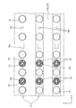
- the difference from the first embodiment further includes a temporary fixing member 25 for fixing the LED substrate 18 to the chassis 14, and the coloring portion 24 is provided in the temporary fixing member insertion hole 18 e through which the temporary fixing member 25 is inserted.
- the rest is not provided, and the others are the same as in the first embodiment.
- the same parts as those in the first embodiment are denoted by the same reference numerals, and redundant description is omitted.
- a plurality of LED units U having LEDs 17 (Light Emitting Diodes) as light sources are accommodated in the chassis 14, and support the optical member 15 and hold the LED substrate 18.
- a support pin 20, a rivet 21 for holding the chassis reflection sheet 22 and the LED board 18, and a temporary fixing member 25 for holding the LED board 18 are provided.
- the chassis 14 has a support pin mounting hole 14d at a position corresponding to the installation position of the support pin 20, and a rivet mounting hole 14e at a position corresponding to the installation position of the rivet 21. Further, a temporary fixing member mounting hole (not shown) is opened at a location corresponding to the installation position of the temporary fixing member 25.
- the LED board 18 has a support pin insertion hole 18c at a position corresponding to the position where the support pin 20 is installed, and a rivet insertion hole at a position corresponding to the position where the rivet 21 is installed. 18d has been established.
- a coloring portion 24 that surrounds the support pin insertion hole 18c and the rivet insertion hole 18d and colors the LED substrate 18.
- the LED board 18 is provided with a temporary fixing member insertion hole 18e at a position corresponding to a position where the temporary fixing member 25 is installed.
- the colored portion 24 is not provided around the temporary fixing member insertion hole 18e. That is, the periphery of the temporary fixing member insertion hole 18 e has a color that can be distinguished from the colored portion 24.
- a temporary fixing member hole 22 e is formed at a position corresponding to the temporary fixing member 25 at the bottom of the chassis reflection sheet 22. Furthermore, a lens hole 22c is opened at a location corresponding to the diffusing lens 19 provided in the LED unit U, and a connector hole 22d is opened at a location corresponding to the connector portion 18a.
- the temporary fixing member hole 22 e has a circular shape when seen in a plan view, and its diameter is set larger than the diameter of the temporary fixing member 25.
- the temporary fixing member 25 is arranged on the bottom plate 14a of the chassis corresponding to a predetermined position of the LED substrate 18, and is made of, for example, a synthetic resin, and the surface thereof exhibits white with excellent light reflectivity.
- the temporary fixing member 25 includes a disk-shaped head and a mounting portion that protrudes downward from the center of the head.
- the attachment portion of the temporary fixing member 25 is a wide portion whose tip can be elastically deformed, and is provided in the temporary attachment member insertion hole 18e provided in the LED board 18 and the temporary attachment member attachment hole provided in the chassis 14. It is inserted and can be locked to the back side of the bottom plate 14a of the chassis.
- the assembly procedure of the backlight device 312 will be described with reference to FIGS.
- the LED board 18 on the right side in the X-axis direction is placed at a predetermined position on the bottom plate 14a of the chassis, as shown in FIG.
- the temporary fixing member 25 temporarily holds the LED substrate 18 with respect to the chassis 14.
- the LED board 18 on the left side in the X-axis direction shown in FIG. 15 is connected to the right LED board 18 by a connector portion 18a, and temporarily held on the chassis 14 by a temporary fixing member 25 (not shown).
- the positions of the support pin insertion holes 18c of the LED board and the support pin mounting holes 14d of the chassis are aligned, and the positions of the rivet insertion holes 18d of the LED board and the rivet mounting holes 14e of the chassis are aligned. ing. Note that the LED 17 is mounted on the LED substrate 18 and a diffusion lens 19 is attached.
- the chassis reflection sheet 22 is placed on the front surface of each LED board 18 so as to face the surface.
- the temporary fixing member 25 passes through the temporary fixing member hole 22e of the chassis reflection sheet.
- the diffusion lens 19 passes through the lens hole 22c of the chassis reflection sheet, and the connector portion 18a passes through the connector hole 22d of the chassis reflection sheet.
- the identification opening 23 of the chassis reflection sheet 22 overlaps with the colored portion 24 of the LED substrate 18, and a part of the colored portion 24 can be visually observed through the opening 23.
- the positions of the support pin holes 22a of the chassis reflection sheet and the support pin insertion holes 18c of the LED board are aligned, and the LED board 18 is formed along the inner periphery of the support pin holes 22a of the chassis reflection sheet. A part of the provided colored portion 24 is visually observed. Further, the positions of the rivet holes 22b of the reflective sheet for chassis and the rivet insertion holes 18d of the LED board are aligned, and are provided on the LED board 18 along the inner periphery of the rivet holes 22b of the reflective sheet for chassis. A part of the colored portion 24 is visually observed.
- the support pins 20 and the rivets 21 are attached as shown in FIG. First, it is visually confirmed that the rivet 21 is a rivet hole 22b having no identification opening 23 in the vicinity, and the position of the rivet hole 22b is confirmed, and the rivet 21 is attached via the rivet hole 22b. After all the rivets 21 have been attached, the support pin 20 is visually confirmed to be a support pin hole 22a with an opening 23 for identification in the vicinity, and the position of the support pin hole 22a is further confirmed. And attached through the support pin hole 22a.
- the rivet mounting portion 21b is fitted and locked to each rivet mounting hole 14e of the chassis via each rivet hole 22b of the chassis reflection sheet and each rivet insertion hole 18d of the LED board, and the rivet 21 is locked to the chassis. 14 is fixed. Further, the support pin mounting portions 20c are fitted and locked into the respective support pin mounting holes 14d of the chassis via the respective support pin holes 22a of the chassis reflection sheet and the respective support pin insertion holes 18c of the LED board. Is fixed to the chassis 14.
- the effect of this embodiment will be described.
- the temporary fixing member 25 the LED substrate 18 can be temporarily held with respect to the chassis 14 when the backlight device 312 is assembled. For this reason, the position of the LED board 18 does not shift at the time of assembly, and the positions of the members and openings provided in the chassis 14, the LED board 18 and the chassis reflection sheet 22 are easily aligned, and the efficiency of the assembly work is improved. Will improve.
- the temporary fixing member insertion hole 18e is supported based on the presence or absence of the colored portion 24. It can be distinguished from the pin insertion hole 18c and the rivet insertion hole 18d. For this reason, it can suppress attaching the temporary fix
- a fifth embodiment of the present invention will be described with reference to FIG.
- the difference from the first embodiment is the shape of the colored portion 424, and the rest is the same as in the first embodiment.
- the same parts as those in the first embodiment are denoted by the same reference numerals, and redundant description is omitted.
- the coloring portion 424 has a shape that matches the shapes of the opening 24, the support pin hole 22 a, and the rivet hole 22 b, and among the front-side surfaces of the LED substrate 18, a chassis reflection sheet 22 that will be described later.
- a chassis reflection sheet 22 that will be described later.
- the opening is formed adjacent to or close to the support pin hole.
- the opening is formed adjacent to or close to either the support pin hole or the rivet hole. It only has to be.
- the diameter of the head of the rivet is configured to be larger than the diameter of the flange of the support pin, and the size of the opening rivets the rivet.
- the opening is hidden in the head of the rivet, while when the support pin is attached to the chassis via the rivet hole and the rivet insertion hole, the opening of the opening is hidden. It is sufficient that the size is at least partially visible.
- the colored portion is black.
- the colored portion is not limited to this, and the colored portion has a different color from the reflective sheet for chassis, and can be distinguished from the reflective sheet. That's fine.
- the colored portion may be blue or red other than black, and the color reflection between the chassis reflection sheet and the colored portion may be different from each other.
- the colored portion is formed on the LED substrate by screen printing.
- the colored portion is not limited to this, and the colored portion is different in color from the chassis reflective sheet and is distinguished from the reflective sheet. It only needs to be possible.
- the substrate on which the LED is mounted may be formed by laser printing at the same time as the serial number of the LED substrate is laser-printed, and a part of the substrate reflection sheet constituting the front side surface of the LED substrate is missing. It may be formed by expressing the color.
- the TFT is used as the switching element of the liquid crystal display device.
- the present invention can also be applied to a liquid crystal display device using a switching element other than TFT (for example, a thin film diode (TFD)), and color display.
- a switching element other than TFT for example, a thin film diode (TFD)
- TFT thin film diode
- the present invention can be applied to a liquid crystal display device that displays black and white.
- the liquid crystal display device using the liquid crystal panel as the display panel has been exemplified, but the present invention is also applicable to a display device using another type of display panel.
- the television receiver provided with the tuner is exemplified.
- the present invention can also be applied to a display device that does not include the tuner.
- SYMBOLS 10 Liquid crystal display device (display device), 11 ... Liquid crystal panel (display panel), 12, 312 ... Backlight device (illumination device), 14 ... Chassis, 14a ... Bottom plate, 14d ... Support pin attachment hole, 14e ... Rivet attachment Hole, 17 ... LED (light source), 18 ... LED substrate (substrate), 18c ... support pin insertion hole (substrate side through hole), 18d ... rivet insertion hole (substrate side through hole), 18e ... temporary fixing member insertion hole, DESCRIPTION OF SYMBOLS 19 ... Diffusing lens, 20 ... Support pin, 21 ... Rivet, 22 ...
- Reflection sheet (reflective sheet) for chassis 22a ... Support pin hole (1st through-hole), 22b ... Rivet hole (2nd through-hole), 23, 123, 223 ... opening, 24, 424 ... colored portion, 25 ... temporary fixing member, TV ... television receiver
Landscapes
- Physics & Mathematics (AREA)
- Nonlinear Science (AREA)
- Optics & Photonics (AREA)
- Crystallography & Structural Chemistry (AREA)
- Chemical & Material Sciences (AREA)
- General Physics & Mathematics (AREA)
- Mathematical Physics (AREA)
- Engineering & Computer Science (AREA)
- Multimedia (AREA)
- Signal Processing (AREA)
- General Engineering & Computer Science (AREA)
- Planar Illumination Modules (AREA)
- Liquid Crystal (AREA)
Abstract
Description
直下型(透過型)のバックライト装置においては、反射シートが浮き上がらないように、リベットにより反射シートを基板(光源ブロック)とともにシャーシに係止する場合がある。支持ピンとリベットの両方を用いたバックライト装置では、支持ピン及びリベットを反射シートと基板を介してシャーシに固定するため、反射シートと基板には支持ピン及びリベットを挿通する貫通孔が設けられている。
上記課題を解決するために、本発明の照明装置は、光源と、前記光源が一面側に実装されてなる基板と、前記基板の他面側を支持するシャーシと、前記基板の前記一面側に配された反射シートと、前記反射シートに対向し、光を拡散する光学部材と、前記反射シートに設けられた第1貫通孔及び第2貫通孔と、前記基板に設けられた基板側貫通孔と、前記第1貫通孔及び前記基板側貫通孔を介して前記シャーシに取り付けられ、前記光学部材を支持する支持ピンと、前記第2貫通孔及び前記基板側貫通孔を介して前記シャーシに取り付けられ、前記反射シートと前記基板とを前記シャーシに固定するためのリベットと、前記反射シートのうち、前記第1貫通孔または前記第2貫通孔のいずれか一方に隣接ないし近接して形成され、前記第1貫通孔と前記第2貫通孔とを識別するための開口部と、前記基板の前記一面のうち、少なくとも前記開口部と重畳する範囲に設けられ、前記反射シートとは色味が異なり、前記反射シートと区別することが可能な着色部と、を備えることに特徴を有する。
本発明によれば、支持ピンとリベットの誤取り付けを抑制し、輝度ムラの発生を抑制可能な照明装置、表示装置、及びテレビ受信装置を提供することが可能となる。
本発明の実施形態1を図1ないし図10によって説明する。本実施形態では、液晶表示装置10について例示する。なお、各図面の一部にはX軸、Y軸及びZ軸が描かれており、各軸方向が各図面で共通した方向となるように描かれている。また、図3に示す上側を表側とし、同図下側を裏側とする。
本発明の実施形態2を図11によって説明する。なお、前記実施形態1との相違は、開口部123の形状及び配置にあり、その他は前記実施形態1と同様である。前記実施形態1と同一部分には、同一符号を付して重複する説明を省略する。
本発明の実施形態3を図12によって説明する。なお、前記実施形態1との相違は、開口部223の形状及び配置にあり、その他は前記実施形態1と同様である。前記実施形態1と同一部分には、同一符号を付して重複する説明を省略する。
本発明の実施形態4を図13から図15によって説明する。なお、前記実施形態1との相違は、LED基板18をシャーシ14に固定するための仮止め部材25をさらに備え、着色部24は、仮止め部材25が挿通される仮止め部材挿通孔18eの周囲には設けられないことにあり、その他は前記実施形態1と同様である。前記実施形態1と同一部分には、同一符号を付して重複する説明を省略する。
本発明の実施形態5を図16によって説明する。なお、前記実施形態1との相違は、着色部424の形状にあり、その他は前記実施形態1と同様である。前記実施形態1と同一部分には、同一符号を付して重複する説明を省略する。
本発明は上記記述及び図面によって説明した実施形態に限定されるものではなく、例えば次のような実施形態も本発明の技術的範囲に含まれる。
Claims (10)
- 光源と、
前記光源が一面側に実装されてなる基板と、
前記基板の他面側を支持するシャーシと、
前記基板の前記一面側に配された反射シートと、
前記反射シートに対向し、光を拡散する光学部材と、
前記反射シートに設けられた第1貫通孔及び第2貫通孔と、
前記基板に設けられた基板側貫通孔と、
前記第1貫通孔及び前記基板側貫通孔を介して前記シャーシに取り付けられ、前記光学部材を支持する支持ピンと、
前記第2貫通孔及び前記基板側貫通孔を介して前記シャーシに取り付けられ、前記反射シートと前記基板とを前記シャーシに固定するためのリベットと、
前記反射シートのうち、前記第1貫通孔または前記第2貫通孔のいずれか一方に隣接ないし近接して形成され、前記第1貫通孔と前記第2貫通孔とを識別するための開口部と、
前記基板の前記一面のうち、少なくとも前記開口部と重畳する範囲に設けられ、前記反射シートとは色味が異なり、前記反射シートと区別することが可能な着色部と、
を備えることを特徴とする照明装置。 - 前記支持ピンに形成された鍔部と、
前記リベットに形成された前記鍔部より小さい頭部とをさらに備え、
前記開口部は、前記第1貫通孔に隣接ないし近接して形成され、前記支持ピンを前記第1貫通孔及び前記基板側貫通孔を介して前記シャーシに取り付けた場合には当該開口部が前記鍔部に隠れる一方、前記リベットを前記第1貫通孔及び前記基板側貫通孔を介して前記シャーシに取り付けた場合には当該開口部の少なくとも一部が視認されることを特徴とする請求項1に記載の照明装置。 - 前記支持ピンに形成された鍔部と、
前記リベットに形成された前記鍔部より大きい頭部とをさらに備え、
前記開口部は、前記第2貫通孔に隣接ないし近接して形成され、前記リベットを前記第2貫通孔及び前記基板側貫通孔を介して前記シャーシに取り付けた場合には当該開口部が前記頭部に隠れる一方、前記支持ピンを前記第2貫通孔及び前記基板側貫通孔を介して前記シャーシに取り付けた場合には当該開口部の少なくとも一部が視認されることを特徴とする請求項1に記載の照明装置。 - 前記着色部は、前記開口部、前記第1貫通孔及び前記第2貫通孔と重畳する範囲に設けられていることを特徴とする請求項1から請求項3のいずれか1項に記載の照明装置。
- 前記基板側貫通孔を介して前記シャーシに取り付けられ、前記基板を前記シャーシに仮止めするための仮止め部材をさらに備え、
前記仮止め部材が挿通される前記基板側貫通孔の周囲は、前記着色部と区別可能な色味とされていることを特徴とする請求項4に記載の照明装置。 - 前記着色部は、前記基板に対して印刷により形成されていることを特徴とする請求項1から請求項5のいずれか1項に記載の照明装置。
- 前記着色部は、前記基板の前記一面のうち、前記開口部、前記第1貫通孔及び前記第2貫通孔と重畳する範囲のみに設けられていることを特徴とする請求項6に記載の照明装置。
- 請求項1から請求項7のいずれか1項に記載の表示装置用照明装置と、この表示装置用照明装置の表側に配される表示パネルとからなる表示装置。
- 前記表示パネルは、一対の基板間に液晶を封入してなる液晶パネルとされる請求項8に記載の表示装置。
- 請求項8または請求項9に記載された表示装置を備えるテレビ受信装置。
Priority Applications (3)
| Application Number | Priority Date | Filing Date | Title |
|---|---|---|---|
| CN201180038102.7A CN103052840B (zh) | 2010-08-19 | 2011-08-09 | 照明装置、显示装置以及电视接收装置 |
| US13/814,889 US9528690B2 (en) | 2010-08-19 | 2011-08-09 | Lighting device, display device and television device |
| JP2012529571A JP5476478B2 (ja) | 2010-08-19 | 2011-08-09 | 照明装置、表示装置及びテレビ受信装置 |
Applications Claiming Priority (2)
| Application Number | Priority Date | Filing Date | Title |
|---|---|---|---|
| JP2010-184055 | 2010-08-19 | ||
| JP2010184055 | 2010-08-19 |
Publications (1)
| Publication Number | Publication Date |
|---|---|
| WO2012023458A1 true WO2012023458A1 (ja) | 2012-02-23 |
Family
ID=45605113
Family Applications (1)
| Application Number | Title | Priority Date | Filing Date |
|---|---|---|---|
| PCT/JP2011/068132 Ceased WO2012023458A1 (ja) | 2010-08-19 | 2011-08-09 | 照明装置、表示装置及びテレビ受信装置 |
Country Status (4)
| Country | Link |
|---|---|
| US (1) | US9528690B2 (ja) |
| JP (1) | JP5476478B2 (ja) |
| CN (1) | CN103052840B (ja) |
| WO (1) | WO2012023458A1 (ja) |
Cited By (3)
| Publication number | Priority date | Publication date | Assignee | Title |
|---|---|---|---|---|
| JP2013246988A (ja) * | 2012-05-25 | 2013-12-09 | Sharp Corp | 照明装置および表示装置 |
| JP2018088008A (ja) * | 2018-02-27 | 2018-06-07 | 船井電機株式会社 | 表示装置 |
| JP2018170292A (ja) * | 2018-07-30 | 2018-11-01 | シャープ株式会社 | バックライト装置、表示装置及びテレビジョン受信機 |
Families Citing this family (9)
| Publication number | Priority date | Publication date | Assignee | Title |
|---|---|---|---|---|
| JP6471590B2 (ja) * | 2015-04-06 | 2019-02-20 | 三菱電機株式会社 | 表示装置 |
| US10371358B2 (en) | 2017-03-06 | 2019-08-06 | Industrial Lighting Products, Llc | LED board mounting system for a light fixture |
| JP2019082535A (ja) * | 2017-10-30 | 2019-05-30 | シャープ株式会社 | 表示装置 |
| KR102520714B1 (ko) | 2018-07-12 | 2023-04-11 | 삼성전자주식회사 | 디스플레이 장치 |
| KR102567522B1 (ko) * | 2018-07-19 | 2023-08-17 | 삼성전자주식회사 | 디스플레이 장치 및 그 제조방법 |
| KR102721663B1 (ko) * | 2019-06-11 | 2024-10-25 | 엘지전자 주식회사 | 반도체 발광소자를 이용한 백라이트 유닛 |
| WO2021218478A1 (zh) * | 2020-04-28 | 2021-11-04 | 海信视像科技股份有限公司 | 一种显示装置 |
| DE112021007950T5 (de) * | 2021-07-12 | 2024-07-04 | Fuji Corporation | Bauteilmontagemaschine und Stützstifthalteverfahren |
| WO2023063439A1 (ko) * | 2021-10-13 | 2023-04-20 | 엘지전자 주식회사 | 디스플레이 디바이스 |
Citations (2)
| Publication number | Priority date | Publication date | Assignee | Title |
|---|---|---|---|---|
| JP2009129707A (ja) * | 2007-11-22 | 2009-06-11 | Sony Corp | バックライト装置及び液晶表示装置 |
| JP4519943B1 (ja) * | 2009-05-22 | 2010-08-04 | シャープ株式会社 | 表示装置 |
Family Cites Families (13)
| Publication number | Priority date | Publication date | Assignee | Title |
|---|---|---|---|---|
| FR2595579B1 (fr) * | 1986-03-14 | 1989-05-05 | Salomon Sa | Ski pourvu de prepercages pour le montage des fixations |
| TWI232337B (en) * | 2003-11-10 | 2005-05-11 | Au Optronics Corp | Direct type backlight module |
| TWI285074B (en) * | 2004-10-01 | 2007-08-01 | Au Optronics Corp | Supporting cone of bottom-lighting backlight module |
| CN1854865A (zh) * | 2005-04-27 | 2006-11-01 | 三菱电机株式会社 | 面状光源装置 |
| JP4821442B2 (ja) | 2006-05-31 | 2011-11-24 | ソニー株式会社 | バックライト装置及び液晶表示装置 |
| TWI344046B (en) * | 2006-10-27 | 2011-06-21 | Hon Hai Prec Ind Co Ltd | Direct type backlight module |
| US8104911B2 (en) * | 2007-09-28 | 2012-01-31 | Apple Inc. | Display system with distributed LED backlight |
| KR101405595B1 (ko) * | 2007-12-18 | 2014-06-12 | 엘지이노텍 주식회사 | 발광 모듈 접속 장치 및 이를 구비한 라이트 유닛 |
| JP4753192B2 (ja) * | 2008-06-27 | 2011-08-24 | Nec液晶テクノロジー株式会社 | 位置合わせ用マーカ、それを用いた表示装置およびその製造方法 |
| JP4780216B2 (ja) * | 2008-10-27 | 2011-09-28 | ソニー株式会社 | 面光源装置とその製造方法、及び画像表示装置 |
| US7905652B2 (en) * | 2008-12-19 | 2011-03-15 | Nei Cheng Tsai | LED string light |
| US20120014093A1 (en) * | 2009-03-23 | 2012-01-19 | Sharp Kabushiki Kaisha | Chassis, lighting device, and display device |
| US20110234424A1 (en) * | 2010-03-25 | 2011-09-29 | Safety Traffic Equipment Co., Ltd. | Led water-proofing diffuser embedded into a shell plate |
-
2011
- 2011-08-09 WO PCT/JP2011/068132 patent/WO2012023458A1/ja not_active Ceased
- 2011-08-09 CN CN201180038102.7A patent/CN103052840B/zh not_active Expired - Fee Related
- 2011-08-09 US US13/814,889 patent/US9528690B2/en not_active Expired - Fee Related
- 2011-08-09 JP JP2012529571A patent/JP5476478B2/ja not_active Expired - Fee Related
Patent Citations (2)
| Publication number | Priority date | Publication date | Assignee | Title |
|---|---|---|---|---|
| JP2009129707A (ja) * | 2007-11-22 | 2009-06-11 | Sony Corp | バックライト装置及び液晶表示装置 |
| JP4519943B1 (ja) * | 2009-05-22 | 2010-08-04 | シャープ株式会社 | 表示装置 |
Cited By (3)
| Publication number | Priority date | Publication date | Assignee | Title |
|---|---|---|---|---|
| JP2013246988A (ja) * | 2012-05-25 | 2013-12-09 | Sharp Corp | 照明装置および表示装置 |
| JP2018088008A (ja) * | 2018-02-27 | 2018-06-07 | 船井電機株式会社 | 表示装置 |
| JP2018170292A (ja) * | 2018-07-30 | 2018-11-01 | シャープ株式会社 | バックライト装置、表示装置及びテレビジョン受信機 |
Also Published As
| Publication number | Publication date |
|---|---|
| CN103052840B (zh) | 2014-11-19 |
| JPWO2012023458A1 (ja) | 2013-10-28 |
| US9528690B2 (en) | 2016-12-27 |
| US20130135539A1 (en) | 2013-05-30 |
| JP5476478B2 (ja) | 2014-04-23 |
| CN103052840A (zh) | 2013-04-17 |
Similar Documents
| Publication | Publication Date | Title |
|---|---|---|
| JP5476478B2 (ja) | 照明装置、表示装置及びテレビ受信装置 | |
| JP5292476B2 (ja) | 照明装置、表示装置、及びテレビ受信装置 | |
| JP5184701B2 (ja) | 照明装置、表示装置、及びテレビ受信装置 | |
| JP4951152B2 (ja) | 照明装置、表示装置、及びテレビ受信装置 | |
| JP5337883B2 (ja) | 照明装置、表示装置、及びテレビ受信装置 | |
| US20130128128A1 (en) | Lighting device, display device and television device | |
| WO2010146913A1 (ja) | 照明装置、表示装置、及びテレビ受信装置 | |
| JP2013143217A (ja) | 照明装置、表示装置、及びテレビ受信装置 | |
| WO2010146917A1 (ja) | 照明装置、表示装置、及びテレビ受信装置 | |
| JP5662952B2 (ja) | 照明装置、表示装置、及びテレビ受信装置 | |
| WO2011148694A1 (ja) | 照明装置、表示装置、及びテレビ受信装置 | |
| WO2011055635A1 (ja) | 光源ユニット用母材、照明装置、表示装置、及びテレビ受信装置 | |
| WO2012165282A1 (ja) | 照明装置、表示装置、及びテレビ受信装置 | |
| US8657458B2 (en) | Lighting device, display device and television receiver | |
| US20070153511A1 (en) | Light source assembly | |
| WO2011089960A1 (ja) | 照明装置、表示装置、及びテレビ受信装置 | |
| WO2013024714A1 (ja) | 照明装置、表示装置、及びテレビ受信装置 | |
| JP2013118055A (ja) | 照明装置、表示装置、及びテレビ受信装置 | |
| WO2013021933A1 (ja) | 照明装置、表示装置、及びテレビ受信装置 | |
| WO2013080882A1 (ja) | 照明装置、表示装置及びテレビ受信装置 | |
| WO2013031674A1 (ja) | 照明装置、表示装置及びテレビ受信装置 | |
| JP2020013721A (ja) | 照明装置、表示装置、及びテレビ受信装置 | |
| WO2011013455A1 (ja) | 照明装置、表示装置、及びテレビ受信装置 | |
| HK1170290A (en) | Lighting device, display apparatus, and television receiving equipment | |
| WO2013047350A1 (ja) | 照明装置、表示装置及びテレビ受信装置 |
Legal Events
| Date | Code | Title | Description |
|---|---|---|---|
| WWE | Wipo information: entry into national phase |
Ref document number: 201180038102.7 Country of ref document: CN |
|
| 121 | Ep: the epo has been informed by wipo that ep was designated in this application |
Ref document number: 11818100 Country of ref document: EP Kind code of ref document: A1 |
|
| ENP | Entry into the national phase |
Ref document number: 2012529571 Country of ref document: JP Kind code of ref document: A |
|
| WWE | Wipo information: entry into national phase |
Ref document number: 13814889 Country of ref document: US |
|
| NENP | Non-entry into the national phase |
Ref country code: DE |
|
| 122 | Ep: pct application non-entry in european phase |
Ref document number: 11818100 Country of ref document: EP Kind code of ref document: A1 |