WO2012014976A1 - 有機電界発光素子 - Google Patents
有機電界発光素子 Download PDFInfo
- Publication number
- WO2012014976A1 WO2012014976A1 PCT/JP2011/067258 JP2011067258W WO2012014976A1 WO 2012014976 A1 WO2012014976 A1 WO 2012014976A1 JP 2011067258 W JP2011067258 W JP 2011067258W WO 2012014976 A1 WO2012014976 A1 WO 2012014976A1
- Authority
- WO
- WIPO (PCT)
- Prior art keywords
- och
- light emitting
- liquid
- emitting layer
- organic
- Prior art date
- Legal status (The legal status is an assumption and is not a legal conclusion. Google has not performed a legal analysis and makes no representation as to the accuracy of the status listed.)
- Ceased
Links
- 0 *[n]1c2ccccc2c2ccccc12 Chemical compound *[n]1c2ccccc2c2ccccc12 0.000 description 3
- RDGQBQYTKWHSTM-LNZAWAQUSA-N CCCCC(CC)COc(c(/C=C/c(cc1)cc2c1c(cccc1)c1[n]2CC)c1)cc(/C=C/C(C(C)C2)=Cc3c2c(CC(C)C=C2)c2[n]3CC)c1OC Chemical compound CCCCC(CC)COc(c(/C=C/c(cc1)cc2c1c(cccc1)c1[n]2CC)c1)cc(/C=C/C(C(C)C2)=Cc3c2c(CC(C)C=C2)c2[n]3CC)c1OC RDGQBQYTKWHSTM-LNZAWAQUSA-N 0.000 description 1
- QXYRRCOJHNZVDJ-UHFFFAOYSA-N OC(CCCc1ccc(cc2)c3c1ccc1c3c2ccc1)=O Chemical compound OC(CCCc1ccc(cc2)c3c1ccc1c3c2ccc1)=O QXYRRCOJHNZVDJ-UHFFFAOYSA-N 0.000 description 1
Images













Classifications
-
- H—ELECTRICITY
- H10—SEMICONDUCTOR DEVICES; ELECTRIC SOLID-STATE DEVICES NOT OTHERWISE PROVIDED FOR
- H10K—ORGANIC ELECTRIC SOLID-STATE DEVICES
- H10K50/00—Organic light-emitting devices
- H10K50/10—OLEDs or polymer light-emitting diodes [PLED]
- H10K50/11—OLEDs or polymer light-emitting diodes [PLED] characterised by the electroluminescent [EL] layers
-
- H—ELECTRICITY
- H10—SEMICONDUCTOR DEVICES; ELECTRIC SOLID-STATE DEVICES NOT OTHERWISE PROVIDED FOR
- H10K—ORGANIC ELECTRIC SOLID-STATE DEVICES
- H10K50/00—Organic light-emitting devices
- H10K50/10—OLEDs or polymer light-emitting diodes [PLED]
- H10K50/11—OLEDs or polymer light-emitting diodes [PLED] characterised by the electroluminescent [EL] layers
- H10K50/12—OLEDs or polymer light-emitting diodes [PLED] characterised by the electroluminescent [EL] layers comprising dopants
-
- H—ELECTRICITY
- H10—SEMICONDUCTOR DEVICES; ELECTRIC SOLID-STATE DEVICES NOT OTHERWISE PROVIDED FOR
- H10K—ORGANIC ELECTRIC SOLID-STATE DEVICES
- H10K50/00—Organic light-emitting devices
- H10K50/10—OLEDs or polymer light-emitting diodes [PLED]
- H10K50/11—OLEDs or polymer light-emitting diodes [PLED] characterised by the electroluminescent [EL] layers
- H10K50/135—OLEDs or polymer light-emitting diodes [PLED] characterised by the electroluminescent [EL] layers comprising mobile ions
-
- H—ELECTRICITY
- H10—SEMICONDUCTOR DEVICES; ELECTRIC SOLID-STATE DEVICES NOT OTHERWISE PROVIDED FOR
- H10K—ORGANIC ELECTRIC SOLID-STATE DEVICES
- H10K50/00—Organic light-emitting devices
- H10K50/10—OLEDs or polymer light-emitting diodes [PLED]
- H10K50/14—Carrier transporting layers
- H10K50/15—Hole transporting layers
-
- H—ELECTRICITY
- H10—SEMICONDUCTOR DEVICES; ELECTRIC SOLID-STATE DEVICES NOT OTHERWISE PROVIDED FOR
- H10K—ORGANIC ELECTRIC SOLID-STATE DEVICES
- H10K71/00—Manufacture or treatment specially adapted for the organic devices covered by this subclass
- H10K71/50—Forming devices by joining two substrates together, e.g. lamination techniques
-
- H—ELECTRICITY
- H10—SEMICONDUCTOR DEVICES; ELECTRIC SOLID-STATE DEVICES NOT OTHERWISE PROVIDED FOR
- H10K—ORGANIC ELECTRIC SOLID-STATE DEVICES
- H10K85/00—Organic materials used in the body or electrodes of devices covered by this subclass
- H10K85/30—Coordination compounds
- H10K85/341—Transition metal complexes, e.g. Ru(II)polypyridine complexes
- H10K85/342—Transition metal complexes, e.g. Ru(II)polypyridine complexes comprising iridium
-
- H—ELECTRICITY
- H10—SEMICONDUCTOR DEVICES; ELECTRIC SOLID-STATE DEVICES NOT OTHERWISE PROVIDED FOR
- H10K—ORGANIC ELECTRIC SOLID-STATE DEVICES
- H10K85/00—Organic materials used in the body or electrodes of devices covered by this subclass
- H10K85/60—Organic compounds having low molecular weight
- H10K85/615—Polycyclic condensed aromatic hydrocarbons, e.g. anthracene
-
- H—ELECTRICITY
- H10—SEMICONDUCTOR DEVICES; ELECTRIC SOLID-STATE DEVICES NOT OTHERWISE PROVIDED FOR
- H10K—ORGANIC ELECTRIC SOLID-STATE DEVICES
- H10K85/00—Organic materials used in the body or electrodes of devices covered by this subclass
- H10K85/60—Organic compounds having low molecular weight
- H10K85/615—Polycyclic condensed aromatic hydrocarbons, e.g. anthracene
- H10K85/622—Polycyclic condensed aromatic hydrocarbons, e.g. anthracene containing four rings, e.g. pyrene
-
- H—ELECTRICITY
- H10—SEMICONDUCTOR DEVICES; ELECTRIC SOLID-STATE DEVICES NOT OTHERWISE PROVIDED FOR
- H10K—ORGANIC ELECTRIC SOLID-STATE DEVICES
- H10K85/00—Organic materials used in the body or electrodes of devices covered by this subclass
- H10K85/60—Organic compounds having low molecular weight
- H10K85/649—Aromatic compounds comprising a hetero atom
- H10K85/655—Aromatic compounds comprising a hetero atom comprising only sulfur as heteroatom
-
- H—ELECTRICITY
- H10—SEMICONDUCTOR DEVICES; ELECTRIC SOLID-STATE DEVICES NOT OTHERWISE PROVIDED FOR
- H10K—ORGANIC ELECTRIC SOLID-STATE DEVICES
- H10K85/00—Organic materials used in the body or electrodes of devices covered by this subclass
- H10K85/60—Organic compounds having low molecular weight
- H10K85/649—Aromatic compounds comprising a hetero atom
- H10K85/657—Polycyclic condensed heteroaromatic hydrocarbons
- H10K85/6576—Polycyclic condensed heteroaromatic hydrocarbons comprising only sulfur in the heteroaromatic polycondensed ring system, e.g. benzothiophene
-
- H—ELECTRICITY
- H10—SEMICONDUCTOR DEVICES; ELECTRIC SOLID-STATE DEVICES NOT OTHERWISE PROVIDED FOR
- H10K—ORGANIC ELECTRIC SOLID-STATE DEVICES
- H10K2101/00—Properties of the organic materials covered by group H10K85/00
- H10K2101/10—Triplet emission
Definitions
- the present invention relates to an organic electroluminescent device, and more particularly, to an organic electroluminescent device including a light emitting layer that is liquid at room temperature.
- An organic electroluminescence element (organic light emitting element) (hereinafter referred to as an organic EL element) has a configuration in which a thin film organic layer (light emitting layer) containing at least one light emitting organic compound is sandwiched between a cathode and an anode.
- this organic EL element is a light-emitting element using a light-emitting organic compound in a light-emitting layer, it is expected to be applied as a display that is lightweight, flexible, inexpensive, and capable of large-area full-color display.
- the light emitting layer used in this organic EL element is driven by three processes: transport of both holes and electrons (charge), formation of excitons by recombination of these carriers, and light emission. Therefore, a material that satisfies these three functions is indispensable for the light emitting layer.
- the material includes a carrier-transporting light emitting material that exhibits these three functions, and a plurality of types to supplement these three functions.
- a carrier transport material / light-emitting material in which organic substances are mixed is used.
- the light emitting material is diluted with the carrier transport material, so that concentration quenching is suppressed and an organic EL device having high light emission efficiency is expected to be obtained. .
- intensive research has been conducted on a wide variety of combinations of light emitting materials and carrier transport materials.
- a method for separating a material that promotes carrier injection, transport, and recombination into a plurality of layers is used as a means for achieving high luminous efficiency of an organic EL element.
- Patent Document 1 reports a hole blocking layer that can be wet-processed. This is because a titanium oxide film is formed between a light emitting layer and a cathode, thereby forming a cathode of a hole. It is possible to reduce the leakage current to the light source and to obtain high luminance and luminous efficiency.
- Non-Patent Document 1 As a technique different from the thin film laminated organic EL element, by adding an organic salt in a polymer light emitting material as disclosed in Non-Patent Document 1, the carrier injection efficiency is improved. It has been reported that a light emitting element with a low driving voltage and high luminance can be obtained.
- the lifetime of the organic EL element is required to be at least 100 cd / m 2 and 100,000 hours, and it can be said that decomposition of organic substances during the period and deterioration of the element due to generated impurities are inevitable.
- the baking of each organic layer causes deterioration of the element, and if one of the organic layers constituting the organic EL element deteriorates, the lifetime of the entire element is greatly increased. Affect. If this deteriorated organic layer has a replaceable structure, for example, by a cartridge or the like, it is considered that a new organic layer can be continuously supplied, and as a result, the organic EL element can be driven semipermanently.
- most of the existing organic EL elements described above use a solid organic thin film, and it is very difficult to replace only the deteriorated organic layer.
- Non-Patent Document 2 reports an organic EL element in which a light emitting layer is liquefied. By making the light emitting layer liquefied or semi-solid, it can be said that the deteriorated liquid light emitting layer is easier to replace than the solid thin film layer, and at least the light emitting layer is considered to be a replaceable light emitting element. .
- the organic EL element in which the light emitting layer is liquefied which is disclosed in Non-Patent Document 2 is hardly an organic EL element exhibiting such high characteristics that it can be replaced with existing lighting or a display. And the device structure needs to be optimized.
- Non-Patent Document 1 is relatively simple such as cathode / light emitting layer / hole injection layer / anode, but as described above, in order to improve the high organic EL characteristics, a thin film is used. There remains room for improvement to a stacked organic EL structure.
- the present invention has been made in view of such circumstances, and provides an organic EL element having a liquid light-emitting layer and having improved EL characteristics such as drive voltage, luminance, current density, and external light emission efficiency. For the purpose.
- the present inventors have found a light-emitting layer that is liquid at room temperature and can maintain a liquid state during both driving and non-driving, and has already reported an organic electroluminescence device (organic EL device) provided with this light-emitting layer.
- organic EL device organic electroluminescence device
- PCT / JP2010 / 062225 this organic EL element had room for further improvement in terms of EL characteristics as described in regard to Non-Patent Document 2 above. Therefore, as a result of intensive studies to further improve the EL characteristics of the organic EL element having a liquid light-emitting layer, the inventors have increased the brightness, by adding an ionic material to the light-emitting layer. It has been found that an organic electroluminescent element (organic EL element) having a low driving voltage and high luminous efficiency can be obtained, and the present invention has been completed.
- An organic electroluminescent device comprising an anode, a cathode, and a light emitting layer that is liquid at room temperature, interposed between each of the electrodes, and the light emitting layer includes an ionic material; 2.
- One organic electroluminescent element in which the light emitting layer is composed of a carrier transport material, a light emitting material, and an ionic material; 4).
- the ionic material is a liquid organic salt, a liquid inorganic salt, an organic salt dispersible in a liquid carrier transporting material or a liquid light emitting material, and an inorganic salt dispersible in a liquid carrier transporting material or a liquid light emitting material 3 organic electroluminescent elements that are one type or two or more types selected from: 5.
- the ionic material comprises a compound represented by the formula [1] (A n + ) i (B m ⁇ ) j [1] [Wherein, A n + represents a cation component having a valence of n (n represents an integer of 1 to 10) and represents a metal ion or an onium ion containing a nitrogen atom, a phosphorus atom, a sulfur atom, or an oxygen atom, B m ⁇ is an m-valent anion component (m represents an integer of 1 to 10) and represents a halide ion, an oxoacid anion, an anion containing a boron atom, an anion containing a phosphorus atom, or an imide anion.
- a n + represents a cation component having a valence of n (n represents an integer of 1 to 10) and represents a metal ion or an onium ion containing a nitrogen atom, a phosphorus atom,
- . i and j are each an integer of 1 to 100 and an integer at which the ionic material represented by the formula [1] becomes electrically neutral. ] 6).
- the hole blocking layer comprises a metal oxide, a metal nitride, a metal sulfide, a metal oxynitride, or a polymer compound; 10.
- the organic electroluminescent element which has a liquid light emitting layer which has a low drive voltage, a high brightness
- the light emitting layer can be kept in a liquid state both when driven and when not driven. For this reason, when the light emitting layer deteriorates, only the light emitting layer may be replaced (for example, cartridge, extraction / reinjection by circulation).
- the light emitting layer is a liquid, the device can be manufactured by using a coating process, and thus can be applied to a lighting device having a large area. Furthermore, it is possible to manufacture a display element having higher flexibility than an organic EL element made of an existing solid organic thin film.
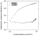
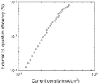
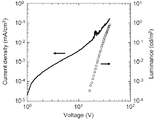
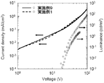
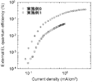
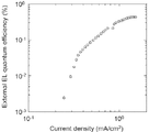
- FIG. 6 is a diagram showing current density-voltage-luminance characteristics of EL elements fabricated in Example 1 and Comparative Example 1. It is a figure which shows the EL external quantum yield-current density characteristic of the EL element produced in Example 1 and Comparative Example 1.
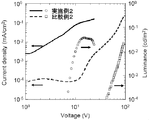
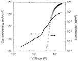
- FIG. 5 is a diagram showing current density-voltage-luminance characteristics of EL elements fabricated in Example 2 and Comparative Example 2.
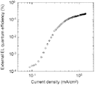
- FIG. 6 is a diagram showing EL external quantum yield-current density characteristics of EL devices fabricated in Example 2 and Comparative Example 2.
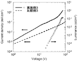
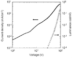
- FIG. 6 is a diagram showing current density-voltage-luminance characteristics of EL elements fabricated in Example 3 and Comparative Example 3.
- FIG. 6 is a diagram showing EL external quantum yield-current density characteristics of the EL device produced in Example 3.
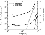
- FIG. 6 is a diagram showing current density-voltage-luminance characteristics of EL elements fabricated in Example 4 and Comparative Example 4.
- FIG. 6 is a diagram showing EL external quantum yield-current density characteristics of EL devices fabricated in Example 4 and Comparative Example 4.
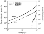
- FIG. 6 is a diagram showing current density-voltage-luminance characteristics of EL elements fabricated in Example 5 and Comparative Example 5.
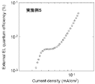
- FIG. 10 is a graph showing EL external quantum yield-current density characteristics of the EL device produced in Example 5.
- FIG. 10 is a graph showing EL external quantum yield-current density characteristics of the EL device produced in Example 5.
- FIG. 10 is a graph showing current density-voltage-luminance characteristics of an EL element manufactured in Example 6.
- FIG. 10 is a graph showing EL external quantum yield-current density characteristics of the EL device produced in Example 6.
- FIG. 10 is a graph showing current density-voltage-luminance characteristics of an EL element manufactured in Example 7.
- FIG. 11 is a graph showing EL external quantum yield-current density characteristics of the EL device produced in Example 7.
- FIG. 10 is a diagram showing current density-voltage-luminance characteristics of an EL element produced in Example 8.
- FIG. 10 is a graph showing EL external quantum yield-current density characteristics of the EL device produced in Example 8.
- FIG. 6 is a diagram showing current density-voltage-luminance characteristics of EL elements fabricated in Example 9 and Example 1.
- FIG. 6 is a diagram showing current density-voltage-luminance characteristics of EL elements fabricated in Example 9 and Example 1.
- FIG. 6 is a diagram showing current density-voltage-luminance characteristics of EL elements fabricated in
- FIG. 6 is a graph showing EL external quantum yield-current density characteristics of the EL devices produced in Example 9 and Example 1.
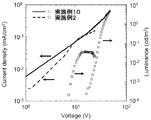
- FIG. 6 is a diagram showing current density-voltage-luminance characteristics of EL elements fabricated in Example 10 and Example 2.
- FIG. 6 is a diagram showing EL external quantum yield-current density characteristics of the EL devices produced in Example 10 and Example 2.
- FIG. 10 is a diagram showing current density-voltage-luminance characteristics of EL elements fabricated in Example 11 and Example 3.
- FIG. 10 is a graph showing EL external quantum yield-current density characteristics of EL devices fabricated in Example 11 and Example 3.
- FIG. 16 is a graph showing current density-voltage-luminance characteristics of an EL element produced in Example 12.
- FIG. 14 is a graph showing EL external quantum yield-current density characteristics of the EL device produced in Example 12.
- FIG. FIG. 16 is a graph showing current density-voltage-luminance characteristics of an EL element produced in Example 13.
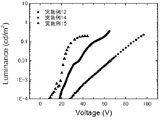
- FIG. 10 is a graph showing EL external quantum yield-current density characteristics of the EL device produced in Example 13. It is a figure which shows the comparison of the luminance-voltage characteristic of the EL element produced in Example 12, 14 and 15. It is a figure which shows the comparison of the luminance-voltage characteristic of the EL element produced in Examples 16-18.
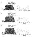
- EL device produced in Example 19 and Example 20 it shows an AFM image of the TiO 2 layer on the ITO cathode, (i) TiO 2 layer without, (ii) the TiO 2 layer 3.5 nm, (iii) TiO 2 Each layer 10 nm is shown.
- EHPy (10 ⁇ m) / ITO (cathode) prepared in Example 21
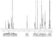
- It is a figure which shows the mode of the light emission at the time of applying. 2 is a 1 H-NMR spectrum diagram of EHPy obtained in Synthesis Example 1.
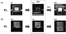
- FIG. 3 is a diagram showing a state in which light emission of the element is restored by injecting the liquid light emitting material again after the liquid light emitting material is made to emit light in the EL element comprising:
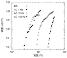
- FIG. 22 is a diagram showing a comparison of luminance-voltage characteristics of the EL element manufactured in Example 23 when a direct current and an alternating voltage are applied.
- the organic electroluminescent element according to the present invention includes an anode, a cathode, and a light emitting layer that is liquid at room temperature and is interposed between these electrodes, and the light emitting layer contains an ionic material.
- the normal temperature means a range of 20 ° C. ⁇ 15 ° C. (5 to 35 ° C.) defined by JIS Z 8703.
- the liquid light-emitting layer may be any liquid-emitting layer as long as it exhibits liquid properties, and at least one of the carrier transport material and the light-emitting material, which are constituent materials of the light-emitting layer, is a liquid, and the composition constituting the light-emitting layer A liquid thing can be used as the whole thing.
- both functions of carrier transport ability and light emission ability cannot be clearly separated.
- some carbazoles, triarylamines, carbon condensed ring dyes and the like have both functions.
- a substance having both of these functions can be used, and any substance that exhibits liquid state can be used alone.
- the compound represented by the formula (1) can be suitably used as the liquid carrier transport material.
- X is a charge transporting part, and is carbazole, triazole, imidazole, oxadiazole, 2,5-diphenyl-1,3,4-oxadiazole, arylcycloalkane, triarylamine, phenylenediamine, Stilbene, oxazole, triphenylmethane, pyrazoline compounds, anthracene, fluorenone, polyaniline, silane, pyrrole, fluorene, porphyrin, quinacridone, triphenylphosphine oxide, anthracene derivatives, tetracene derivatives, pyrene derivatives, rubrene derivatives, decacyclene derivatives, perylene derivatives And carbon condensed ring system dyes such as metal or metal-free phthalocyanine, metal or metal-free naphthalocyanine, and benzidine.
- carbazole is preferable because it has excellent hole transport performance.
- Y is at least one substituent linked to the charge transport part X, and may contain an ether bond, a thioether bond, an ester bond, a carbonate bond or an amide bond.
- These ether bonds, thioether bonds, ester bonds, carbonate ester bonds, and amide bonds may be present at the connecting portion of X and Y (this also applies to Z described later).
- the alkyl group may be linear, branched or cyclic. However, when a linear alkyl group is used, the crystallinity is improved and the viscosity is increased by intermolecular interaction such as packing of alkyl chains. Since an increase is considered, a branched alkyl group is more preferable.
- alkyl group having 1 to 30 carbon atoms examples include methyl, ethyl, n-propyl, i-propyl, c-propyl, n-butyl, i-butyl, s-butyl, t-butyl, c -Butyl, n-pentyl, 1-methyl-n-butyl, 2-methyl-n-butyl, 3-methyl-n-butyl, 1,1-dimethyl-n-propyl, c-pentyl, 2-methyl-c -Butyl, n-hexyl, 1-methyl-n-pentyl, 2-methyl-n-pentyl, 1,1-dimethyl-n-butyl, 1-ethyl-n-butyl, 1,1,2-trimethyl-n -Propyl, c-hexyl, 1-methyl-c-pentyl, 1-ethyl-c-butyl, 1,2-dimethyl-c-
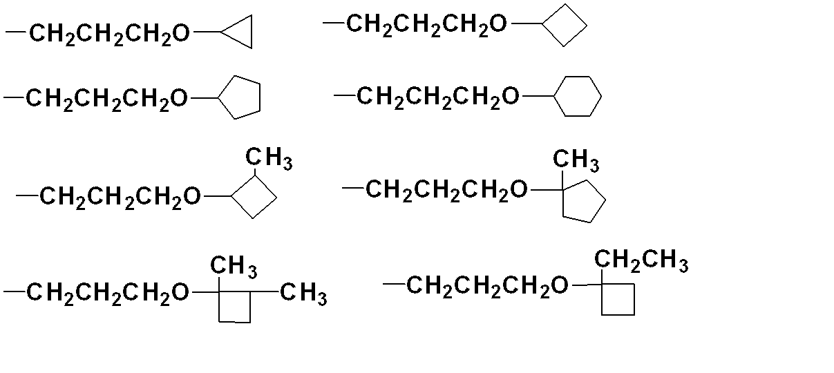
- alkyl group having 1 to 30 carbon atoms including an ether bond, a thioether bond, an ester bond, a carbonate ester bond or an amide bond examples include those having these bonds at any position of the alkyl group as described above. Specific examples include the following substituents.
- a carrier transporting material that dissolves an ionic material well can be obtained.
- alkyl group containing an ether bond examples include CH 2 OCH 3 , CH 2 OCH 2 CH 3 , CH 2 O (CH 2 ) 2 CH 3 , CH 2 OCH (CH 3 ) 2 , and CH 2 O.
- alkyl group containing a thioether bond examples include a group in which the oxygen atom (O) of the alkyl group containing the ether bond is replaced with a sulfur atom (S).
- alkyl group containing an ester bond examples include groups in which the oxygen atom (O) of the alkyl group containing an ether bond is replaced with C (O) O or OC (O).
- alkyl group containing a carbonate bond include a group in which the oxygen atom (O) of the alkyl group containing an ether bond is replaced with OC (O) O.
- the oxygen atom (O) of the alkyl group containing an ether bond was replaced with C (O) NH or NHC (O).
- a substituent having 6 to 30 carbon atoms is preferable from the viewpoint of easily becoming a liquid.
- CH 2 CH 2 OCH 2 CH 2 OCH 3 CH 2 CH 2 OCH 2 CH 2 OCH 2 CH 2 OCH 3 , CH 2 CH 2 OCH 2 CH 2 OCH 2 CH 2 OCH 3 , CH 2 CH 2 OCH 2 CH 2 OCH 2 CH 2 OCH 2 CH 2 OCH 3 , CH 2 CH 2 OCH 2 CH 2 OCH 2 CH 2 OCH 2 CH 2 OCH 3 , CH 2 CH 2 OCH 2 CH 2 OCH 2 CH 2 OCH 2 CH 2 OCH 3 , CH 2 CH 2 OCH 2 CH 2 OCH 2 CH 2 OCH 2 CH 2 OCH 2 CH 2 OCH 3 , CH 2 CH 2 OCH 2 CH 2 OCH 2 CH 2 OCH 2 CH 2 OCH 2 CH 2 OCH 3 , CH 2 CH 2 CH 2 OCH 2 CH 2 OCH 3 , CH 2 CH 2 CH 2 OCH 2 CH 2 CH 2 OCH 3 , CH 2 CH 2 CH 2 OCH 2 CH 2 CH 2 OCH 3 , CH 2 CH 2 CH 2 OCH 2 CH 2 OCH 3 , CH 2 CH 2 CH 2
- Suitable carrier transporting materials include, for example, the following carbazole (X1), N, N-disubstituted or N, N, N-trisubstituted arylamine (X2).
- Y 1 to Y 6 each independently represent a hydrogen atom or an alkyl group having 1 to 30 carbon atoms which may contain an ether bond, thioether, ester bond, carbonate bond or amide bond ( Provided that at least one of Y 1 to Y 3 and at least one of Y 4 to Y 6 is the above alkyl group), A 1 and A 2 represent a single bond or a substituted or unsubstituted aromatic ring. To express.
- alkyl group includes linear, branched, and cyclic alkyl such as methyl, ethyl, isopropyl, t-butyl, 2-ethylhexyl, and cyclohexyl, which has a melting point of the above general formula (1).
- Y functional group for lowering
- specific examples and preferred examples thereof are as described above.
- the aromatic ring include a benzene ring and a naphthalene ring.
- Y 1 , Y 2 , Y 4 and Y 5 are hydrogen atoms
- Y 3 and Y 6 are alkyl
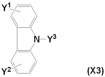
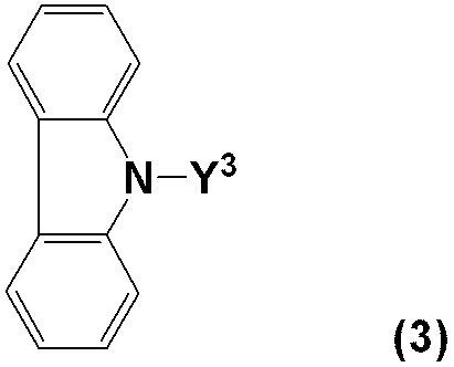
- a 1 , A 2 is preferably a benzene ring or a single bond. From these points, the following compound (X3) is preferable, the compound (3) is more preferable, and the compound (4) or the compound (5) is more preferable, but is not limited thereto.
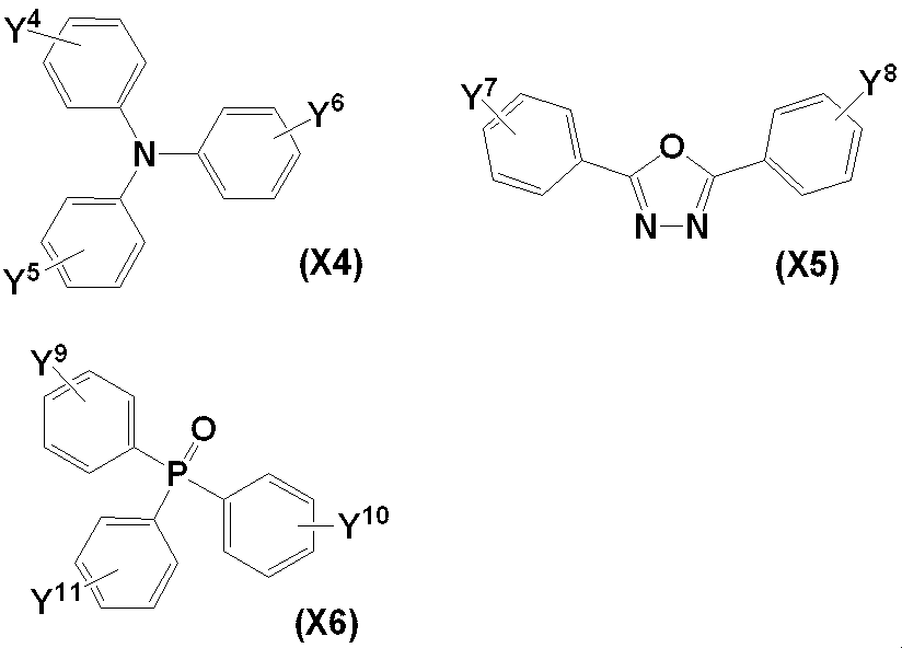
- Y 4 to Y 11 each independently represents a hydrogen atom or an alkyl group having 1 to 30 carbon atoms which may contain an ether bond, a thioether, an ester bond, a carbonate ester bond, an amide bond or the like (provided that , At least one of Y 4 to Y 6 , at least one of Y 7 and Y 8 , and at least one of Y 9 to Y 11 is the above alkyl group.)
- R 1 to R 4 each independently represent an alkyl group having 1 to 30 carbon atoms.
- a solid thing can also be used at normal temperature as a carrier transport material.
- a carrier transport material may be appropriately selected from conventionally known materials.
- the light emitting material which is the other material constituting the light emitting layer of the present invention may be appropriately selected from known materials.
- carbon condensed rings such as anthracene derivatives, tetracene derivatives, pyrene derivatives, rubrene derivatives, decacyclene derivatives, etc.
- Perylene derivatives such as perylene diimide; xanthene dyes such as rhodamine B; cyanine dyes; coumarin dyes such as coumarin 6 and C545T; quinacridone dyes such as Qd4 and DEQ; squalium dyes; styryl dyes; Derivatives; Phenoxazone dyes such as NileRed; carbazole; triarylamine; tris (2-phenylpyridine) iridium (III) (Ir (ppy) 3 ), tris [2-phenyl-4- (2-ethylcyclohexyloxy) pyridine Iridium (III) (Ir ehppy) 3) iridium complex and the like; aluminum quinolinol complexes, benzoquinolinol beryllium complexes, benzoxazolyl zinc complexes, benzothiazole zinc complexes, azomethyl zinc complexes, porphyrin zinc complexes, such as
- a liquid compound represented by the formula (2) can also be used as the light emitting material.
- Z is a dye part, and is a carbon condensed ring dye, perylene derivative, xanthene dye, cyanine dye, coumarin dye, quinacridone dye, squalium dye, styryl dye, pyrazolone derivative, phenoxazone derivative.
- D represents a metal complex composed of a ligand, a carbazole, a triarylamine, an iridium complex, a central metal composed of Al, Zn, Be, or a rare earth metal and a ligand
- W represents at least one substitution linked to the pigment part Z
- alkyl group having 1 to 30 carbon atoms which may include an ether bond, a thioether bond, an ester bond, a carbonate ester bond or an amide bond.
- Specific examples of the dye portion and the alkyl group include the same ones as described above.
- Z include carbon condensed ring dyes, particularly rubrene derivatives and pyrene derivatives
- W include alkyl groups having 1 to 30 carbon atoms, particularly alkyl groups having 6 to 30 carbon atoms. It is done.
- Specific examples of the light-emitting material include the following pyrene derivative (Z1), which is a carbon condensed ring dye having excellent light emission characteristics.
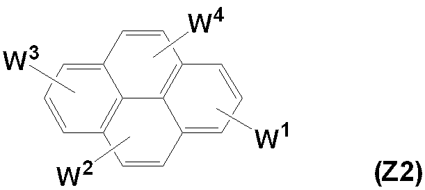
- W 1 to W 4 each independently represent a hydrogen atom or an alkyl group having 1 to 30 carbon atoms which may contain an ether bond, a thioether, an ester bond, a carbonate ester bond, an amide bond, or the like ( Provided that at least one of W 1 to W 4 is the above alkyl group), and A 1 to A 4 each represents a single bond or a substituted or unsubstituted aromatic ring.
- specific examples of the alkyl group include those similar to the above Y, and specific examples of the aromatic ring include those similar to the above.
- a compound in which A 1 to A 4 are single bonds that is, a compound (Z2) in which W 1 to W 4 are directly bonded to a carbon condensed ring is preferable. Further, it is more preferable that at least one of W 1 to W 4 is a hydrogen atom, and particularly, three is a hydrogen atom. From these points, the following compound (Z3) is preferable, but is not limited thereto.
- An organic EL device having a light emitting layer that is not a host guest system can be obtained by using the compounds represented by (Z1) to (Z3) as a liquid light emitting material.
- a light-emitting material that is solid at room temperature can be used as long as the entire material constituting the light-emitting layer is liquid.
- a light emitting material may be appropriately selected from conventionally known materials. For example, tris (8-quinolinolato) aluminum (III) (Alq 3 ), bis (8-quinolinolato) zinc (II) (Znq 2 ), Bis (2-methyl-8-quinolinolato) (p-phenylphenolate) aluminum (III) (BAlq), 4,4′-bis (2,2-diphenylvinyl) biphenyl (DPVBi), and the like.
- the ionic material used together with the liquid luminescent material is not particularly limited as long as it is an ionic material. At least one of the above-described liquid luminescent material and carrier transport material is used. An ionic material that dissolves or disperses may be appropriately selected and used. Specific examples thereof include a compound represented by the following formula [1].
- a n + is a cation component having a valence of n (n represents an integer of 1 to 10) and represents a metal ion or an onium ion containing a nitrogen atom, a phosphorus atom, a sulfur atom or an oxygen atom
- B m ⁇ is an m-valent anion component (m represents an integer of 1 to 10) and represents a halide ion, an oxoacid anion, an anion containing a boron atom, an anion containing a phosphorus atom, or an imide anion.
- . i and j are each an integer of 1 to 100 and an integer at which the ionic material represented by the formula [1] becomes electrically neutral.
- onium ions containing a nitrogen atom examples include tetraalkylammonium cations such as tetramethylammonium cation, tetraethylammonium cation, tetra (n-butyl) ammonium cation, and 1- (n-butyl) -1-methylpyrrolidinium cation; N N, N′-dimethylimidazolium cation, N, N′-ethylmethylimidazolium cation, N, N′-dialkylimidazolium cation such as N, N′-butylmethylimidazolium cation, and the like.
- Examples of the onium ion containing a phosphorus atom include tetraalkylphosphonium cations such as tetramethylphosphonium cation, tetraethylphosphonium cation and tetra (n-butyl) phosphonium cation; PH 4 + and the like.
- Examples of the onium ion containing a sulfur atom include trialkylsulfonium cations such as trimethylsulfonium cation, triethylsulfonium cation, and tri (n-butyl) sulfonium cation.
- Examples of the onium ion containing an oxygen atom include trialkyloxonium cations such as trimethyloxonium cation, triethyloxonium cation, and tri (n-butyl) oxonium cation.
- Examples of the halide ion include F ⁇ , Cl ⁇ , Br ⁇ , and I ⁇ .
- Examples of the oxo acid anion include a borate anion, a carbonate anion, an acetate anion, a sulfate anion, and a phosphate anion.
- Examples of the anion containing a boron atom include BF 4 ⁇ ; tetraalkyl borates such as tetramethyl borate and tetraethyl borate; and tetraaryl borates such as tetraphenyl borate and tetrakis (pentafluorophenyl) borate.
- the imide anion include bis (perfluoroalkanesulfonyl) imide anion such as bis (trifluoromethanesulfonyl) imide anion.
- the ionic material include tetra (n-butyl) ammonium hexafluorophosphate, 1- (n-butyl) -1-methylpyrrolidinium bis (trifluoromethanesulfonyl) imide, 1- (n-propyl) Tetraalkylammonium salts such as -1-methylpyrrolidinium bis (trifluoromethanesulfonyl) imide; imidazolium salts such as N, N'-butylmethylimidazolium hexafluorophosphate; tetra (n-butyl) phosphonium bis (trifluoro) Tetraalkylphosphonium salts such as (romethanesulfonyl) imide, tri (n-butyl) methylphosphonium bis (trifluoromethanesulfonyl) imide; trialkylsulfonium such as triethylsulfonium bis (trifluoromethane) im
- an organic salt having an onium ion containing a nitrogen atom, a phosphorus atom, a sulfur atom or an oxygen atom is preferable, and has an onium ion containing a nitrogen atom.
- Organic salts are preferred, especially tetra (n-butyl) ammonium hexafluorophosphate, 1-butyl-1-methylpyrrolidinium bis (trifluoromethanesulfonyl) imide, 1-propyl-1-methylpyrrolidinium bis (trifluoromethane) Sulfonyl) imide and the like are preferred.
- the addition amount of the ionic material is not particularly limited, but in the present invention, a small amount of about 0.01 to 50% by mass, preferably 0.1 to 1.0% by mass is added to the light emitting layer. However, a sufficient effect can be exhibited.
- the method of mixing the light emitting material or the carrier transport material and the ionic material is arbitrary, but when a solid component is used, a method of mixing the solid component with the liquid component is preferable.
- the organic electroluminescent element of the present invention since the above-described liquid light emitting layer is characterized, there are no particular limitations on the constituent members of the other elements, and conventionally known elements can be appropriately employed.
- a transparent electrode typified by indium tin oxide (ITO) or indium zinc oxide (IZO), a polythiophene derivative having high charge transportability, a polyaniline derivative, or the like can be used.
- the cathode material aluminum, magnesium-silver alloy, aluminum-lithium alloy, lithium, sodium, potassium, cesium, cesium-added ITO, or the like can be used.
- the organic electroluminescent element of this invention employs a function separation type thin film structure provided with at least 3 layers of functional layers containing a light emitting layer between an anode and a cathode.
- a functional layer include a hole transport layer, a hole injection layer, an electron transport layer, an electron injection layer, a carrier block layer (hole block layer, electron block layer), and the like.
- the hole transport layer is a layer that is provided between the anode and the light emitting layer and has a function of transporting holes injected from the anode to the light emitting layer.
- the thing similar to a hole transport material is mentioned.
- the hole injection layer is a layer that is provided between the hole transport layer and the anode and has a function of increasing the hole injection efficiency from the anode. Examples of the material for forming the hole injection layer include copper phthalocyanine, 4,4 ′, 4 ′′ -tris [3-methylphenyl (phenyl) amino] triphenylamine (m-MTDATA), and the like.
- the electron transport layer is a layer that is provided between the cathode and the light emitting layer and has a function of transporting electrons injected from the cathode to the light emitting layer.
- the electron transport material exemplified in the carrier transport material is used. The same thing is mentioned.
- the electron injection layer is a layer that is provided between the electron transport layer and the cathode and has a function of increasing the efficiency of electron injection from the cathode.
- lithium oxide Li 2 O
- magnesium oxide MgO
- alumina Al 2 O 3
- lithium fluoride LiF
- magnesium fluoride MgF 2
- strontium fluoride SrF 2
- Li (acac) Li (acac)
- lithium acetate lithium benzoate
- the carrier block layer is a layer for controlling the light emitting region, and can be formed between any of the above-described layers.
- the material that can be used for the hole blocking layer is not particularly limited as long as it can inhibit the movement of holes from the liquid light emitting layer and is insoluble in the liquid light emitting layer.
- metal oxides, metal nitrides, metal sulfides, metal oxynitrides, and polymer compounds used in the block layer are preferable.
- the metal oxide, metal nitride, metal sulfide, and metal oxynitride include Ti, Zr, Ba, Ca, Sr, Yb, Al, Ga, In, Li, Na, Cd, Mg, Si, and Ta.
- oxides, nitrides, sulfides, and oxynitrides containing at least one metal element selected from Sb, and among these, titanium oxide, zirconium oxide, zinc sulfide, cadmium sulfide, and the like are more preferable.
- the polymer compound include aniline copolymers, oligo or polythiophene, polythiophene derivatives, polyphenylene derivatives, polyphenylene vinylene derivatives, polyfluorene derivatives, and the like.
- the hole block layer is formed by a vacuum method, a dry method such as a sputtering method, an inkjet method, a casting method, a dip coating method, a bar coating method, a blade coating method, a roll coating method, a gravure coating method, a flexographic printing method, It can be performed by a wet method such as a spray coating method.
- the film thickness of the hole blocking layer is preferably about 1 to 1000 nm, more preferably about 5 to 50 nm, from the viewpoint of ensuring sufficient hole blocking capability and preventing an increase in driving voltage.
- organic electroluminescent element of the present invention can be driven by either a DC voltage or an AC voltage.
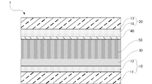
- FIG. 1 shows an organic EL element 1 which is an electroluminescent element according to an embodiment of the present invention.
- the organic EL element 1 includes an anode 10, a hole injection layer 30 laminated on the anode 10, a cathode 20, a hole blocking layer 40 laminated on the cathode 20, the hole injection layer 30 and the holes.
- a light emitting layer 50 that is liquid at room temperature and contains an ionic material (hereinafter referred to as a liquid light emitting layer 50) is provided between the block layers 40.
- the anode 10 is composed of a glass substrate 11 and an ITO substrate 12 formed thereon.
- the cathode 20 is composed of a glass substrate 13 and an ITO substrate 14 formed thereon.
- the hole block layer 40 is made of titanium oxide, and the hole injection layer 30 is made of a PEDOT: PSS film.
- the liquid light-emitting layer 50 includes a carrier transport material, a light-emitting material, and an ionic material.
- a carrier transport material a carrier transport material
- a light-emitting material a light-emitting material
- an ionic material a carrier transport material.
- 9- (2-ethylhexyl) carbazole (EHCz) that is a liquid carrier transport material and normal temperature are used. It comprises rubrene, which is a solid light emitting material, and tetrabutylammonium hexafluorophosphate (TBAPF 6 ), which is a solid ionic material at room temperature.
- rubrene which is a solid light emitting material
- TAPF 6 tetrabutylammonium hexafluorophosphate
- PEDOT PSS is applied on the anode 10 by spin coating, and this is heated to form the hole injection layer 30.
- titanium oxide is laminated on the laminated body of the glass substrate 13 and the ITO substrate 14 by a sputtering method, and the hole block layer 40 is formed.
- a 9- (2-ethylhexyl) carbazole (EHCz) solution containing a predetermined amount of rubrene and TBAPF 6 is dropped on the anode 10 (hole injection layer 30) to form a liquid light emitting layer 50,
- the organic EL element 1 is obtained by pressing the cathode 20 on which the hole block layer 40 is laminated with an appropriate pressure.
- each layer is not limited to the material used by the said embodiment, As long as the function of each layer is exhibited, it can select from the various materials illustrated previously suitably and can be used.
- the method for forming each layer is not limited to the method of the above embodiment, and a known method such as an evaporation method, a spray method, an ink jet method, or a sputtering method can be appropriately employed depending on the material to be used.
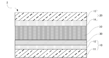
- the hole block layer, the hole injection layer, and the like are layers formed as necessary. For example, as shown in FIG. 2, a configuration like the organic EL element 2 that does not have the hole block layer is adopted. You can also
- Matrix-assisted laser desorption / ionization time-of-flight mass spectrometry Matrix-assisted laser desorption / ionization time-of-flight mass spectrometer (MALDI- TOF-MS), Autoflex-III.
- AFM Atomic force microscope
- JSPM-5400 Scanning probe microscope
- JSPM-5400 Scanning probe microscope
- JSPM-5400 Scanning probe microscope
- Voltage-luminance characteristics during application of AC voltage A voltage amplifier HGH SPEED BIPOLAR AMPLIFIER 4101
- AC power supply A & D Corporation, SWEEP FUNCTION GENERATOR AD-8623
- Example 1 Improvement of device characteristics by adding salt in host guest system
- EHCz 83.2 parts by mass of 9- (2-ethylhexyl) carbazole (hereinafter referred to as EHCz), 16.7 parts by mass of guest compound 2 obtained in Synthesis Example 3, and tetra as an ionic material
- a liquid luminescent material was prepared by adding 0.1 part by mass of butylammonium hexafluorophosphate (hereinafter, TBAPF 6 ) and completely dissolving guest compound 2 and TBAPF 6 in EHCz.
- TBAPF 6 butylammonium hexafluorophosphate
- the EL element was produced as follows. Two ITO glass substrates prepared by ultrasonic cleaning in the order of surfactant, pure water, and isopropanol, and subjected to UV / ozone treatment (manufactured by Filgen, UV253S) for 12 minutes were prepared. One glass substrate 11 with ITO 12 is formed by spin-coating PEDOT: PSS (manufactured by Bayer, PI4083) at a rotational speed of 3000 rpm for 30 seconds, and then heated in air at 200 ° C. for 10 minutes to inject holes. The anode side substrate 10 in which the layer 30 was formed on the ITO 12 was obtained.
- PEDOT: PSS manufactured by Bayer, PI4083
- the cathode side substrate 20 made of the other glass substrate 13 with ITO 14 is put in a glove box, and a small amount of the previously prepared liquid light emitting material is dropped on the side on which the ITO 14 is formed to form PEDOT: PSS.
- the EL element 2 made of a glass substrate was produced. The element area is 2 mm ⁇ 2 mm.
- the current density-voltage-luminance and emission spectrum of the produced EL element were measured. The results are shown in FIG. 3 and FIG. It was 1100 nm when the film thickness of the liquid light emitting layer of this device was computed from the result of permittivity measurement. As shown in FIGS. 3 and 4, the emission was observed from 18.0 V, a current density of 0.99 mA / cm 2 when 62.0 V was applied, a maximum luminance of 2.3 cd / m 2 , and 0.051% The EL external quantum efficiency was obtained. Further, green electroluminescence having an emission peak at 531 nm was obtained.
- Example 1 An EL element was prepared in the same manner as in Example 1 except that TBAPF 6 was not added to the liquid light emitting material, and the same evaluation was performed. The results are shown in FIGS. It was 1100 nm when the film thickness of the liquid light emitting layer of this device was computed from the result of permittivity measurement. As shown in FIGS. 3 and 4, emission is observed from 34.1 V, current density of 0.95 mA / cm 2 when 79 V is applied, maximum luminance of 0.015 cd / m 2 , EL external quantum of 0.00034% Efficiency was obtained, and green light emission having an emission peak at 531 nm was obtained as in Example 1.
- Example 2 The EHCz98.9 parts by mass as a guest compound 5,6,11,12-tetraphenyl naphthacene (hereinafter, rubrene) 1.0 part by weight, TBAPF 6 0.1 parts by mass of the rubrene and TBAPF 6 in EHCz A liquid light emitting material was prepared by completely dissolving. An EL element was produced in the same manner as in Example 1 except that the liquid light emitting material was used, and the same evaluation was performed. The results are shown in FIG. 5 and FIG. It was 380 nm when the film thickness of the liquid light emitting layer of this device was computed from the result of permittivity measurement. As shown in FIG. 5 and FIG.
- Example 2 An EL element was prepared in the same manner as in Example 2 except that TBAPF 6 was not added to the liquid light emitting material, and evaluation was performed in the same manner. The results are shown in FIGS. It was 530 nm when the film thickness of the liquid light emitting layer of this device was computed from the result of permittivity measurement. As shown in FIG. 5 and FIG. 6, light emission is observed from 40.1 V, current density of 0.21 mA / cm 2 when 93.2 V is applied, maximum luminance of 0.023 cd / m 2 , 0.0048% The EL external quantum efficiency was obtained, and orange light emission having an emission peak of 557 nm was obtained in the same manner as in Example 2.
- Example 3 An EL device was prepared in the same manner as in Example 1 except that the guest compound 1 was not added to the liquid light emitting material, and the same evaluation was performed. The results are shown in FIGS. It was 800 nm when the film thickness of the liquid light emitting layer of this device was computed from the result of permittivity measurement. As shown in FIGS.
- Example 3 An EL element was prepared in the same manner as in Example 3 except that TBAPF 6 was not added to the liquid light emitting material, and the same evaluation was performed. It was 900 nm when the film thickness of the liquid light emitting layer of this device was computed from the result of permittivity measurement. As shown in FIG. 7, in this device, a current density of 0.11 mA / cm 2 was obtained when 100 V was applied, but no light emission was observed.
- Example 4 An EL device was prepared in the same manner as in Example 1 except that a liquid light-emitting material composed of 99.9 parts by mass of the liquid host compound EHPy obtained in Synthesis Example 1 and 0.1 part by mass of TBAPF 6 was used. went. The results are shown in FIG. 9 and FIG. It was 1150 nm when the film thickness of the liquid light emitting layer of this device was computed from the result of permittivity measurement. As shown in FIG. 9 and FIG. 10, light emission was observed from 18.4 V, current density of 146 mA / cm 2 when 64.4 V was applied, maximum luminance of 416 cd / m 2 , and 2.9 mA / cm when 46.8 V was applied. A current density of cm 2 and a maximum EL external quantum efficiency of 0.13% were obtained, and blue-green electroluminescence having a peak at 486 nm was obtained.
- Example 4 An EL element was produced in the same manner as in Example 4 except that TBAPF 6 was not added, and the same evaluation was performed. The results are shown in FIG. 9 and FIG. It was 690 nm when the film thickness of the liquid light emitting layer of this device was computed from the result of permittivity measurement. As shown in FIGS. 9 and 10, electroluminescence is observed from 60.8 V, current density of 0.067 mA / cm 2 when 100 V is applied, maximum brightness of 0.58 cd / m 2 , EL of 0.23% External quantum efficiency was obtained, and blue-green electroluminescence having an emission peak at 486 nm was obtained as in Example 4.
- a comparison between Examples 3 and 4 and Comparative Examples 3 and 4 shows that an organic salt is added to a liquid light-emitting material even in an EL device using a liquid light-emitting material as a light-emitting layer as a liquid compound having both charge transporting properties and light-emitting properties. It can be seen that the driving voltage is reduced and the luminance and the external quantum efficiency of the EL are improved.
- Example 5 An EL device was produced in the same manner as in Example 5 except that TBAPF 6 was not added, and the same evaluation was performed. It was 930 nm when the film thickness of the liquid light emitting layer of this device was computed from the result of permittivity measurement. From this device, as shown in FIG. 11, a current density of 0.19 mA / cm 2 was obtained when 100 V was applied, but no light emission was observed.
- Example 5 and Comparative Example 5 are compared with each other, even in a liquid light-emitting material in which a phosphorescent dye is dissolved in a liquid host, when an organic salt is added, the driving voltage decreases, resulting in luminance and EL. It can be seen that both the external quantum efficiencies are improved and good light emission characteristics can be obtained.
- Example 6 System using other guest compound or host compound
- a liquid comprising 89.9 parts by mass of Cz-TEG represented by the following formula as a host compound, 10.0 parts by mass of guest compound 3 (manufactured by American Daisell) represented by the following formula as a guest compound, and 0.1 part by mass of TBAPF 6
- An EL element was produced in the same manner as in Example 1 except that the light emitting material was used, and the same evaluation was performed. The results are shown in FIG. 13 and FIG. It was 1090 nm when the film thickness of the liquid light emitting layer of this device was computed from the result of permittivity measurement. As shown in FIG. 13 and FIG.
- Example 7 Implementation was performed except that 69.9 parts by mass of Cz-TEG, 30.0 parts by mass of guest compound 4 (manufactured by American Dice Source) represented by the following formula, and 0.1 part by mass of TBAPF 6 were used as guest compounds.
- An EL element was produced in the same manner as in Example 1, and the same evaluation was performed. The results are shown in FIG. 15 and FIG. It was 1090 nm when the film thickness of the liquid light emitting layer of this device was computed from the result of permittivity measurement. As shown in FIG. 15 and FIG.
- Example 8 Other than using 79.9 parts by mass of Cz-TEG, 20.0 parts by mass of guest compound 5 (manufactured by American Dye Source) represented by the following formula as a guest compound, and 0.1 part by mass of TBAPF 6.
- a guest compound manufactured by American Dye Source
- TBAPF 6 0.1 part by mass of TBAPF 6.
- Example 9 Improvement of external quantum efficiency of light emission by hole blocking layer
- Two ITO glass substrates were prepared by ultrasonic cleaning in the order of surfactant, pure water and isopropanol, and then UV / ozone treatment (manufactured by Filgen, UV253S) for about 12 minutes.
- One glass substrate 11 with ITO 12 is formed by spin-coating PEDOT: PSS (manufactured by Bayer, PI4083) at 3000 rpm for 30 seconds and then heating in the atmosphere at 200 ° C. for 10 minutes to form a hole injection layer.
- the anode side substrate 10 in which 30 was formed on the ITO 12 was obtained.
- a TiO 2 film having a thickness of 10 nm was formed by sputtering to obtain a cathode-side substrate 20 on which the hole blocking layer 40 was formed.
- a small amount of the liquid light emitting material similar to that of Example 1 is dropped on the hole block layer 40, sandwiched with the anode side substrate 10 on which PEDOT: PSS is formed, and fixed with a clip (not shown).
- an EL element 1 made of glass substrate / ITO (anode) / PEDOT: PSS 40 nm / liquid light emitting layer / TiO 2 (hole block layer) 10 nm / ITO (cathode) / glass substrate was produced.
- the element area is 2 mm ⁇ 2 mm. It was 1100 nm when the film thickness of the liquid light emitting layer of this device was computed from the result of permittivity measurement.
- the current density, luminance, voltage, EL external quantum efficiency, and emission spectrum were evaluated. The results are shown in FIG. 19 and FIG. As shown in FIG. 19 and FIG. 20, light emission is observed from 15.0 V, current density of 3.72 mA / cm 2 when 100 V is applied, maximum brightness of 76.8 cd / m 2 , maximum brightness of 0.37% EL external quantum efficiency was obtained, and green electroluminescence having an emission peak of 531 nm was obtained as in Example 1.
- Example 10 An EL element was prepared in the same manner as in Example 9 except that a liquid light emitting material composed of 98.9 parts by mass of EHCz, 1.0 part by mass of rubrene and 0.1 part by mass of TBAPF 6 was used as a guest compound, and the same evaluation was performed. It was. The results are shown in FIG. 21 and FIG. It was 1210 nm when the film thickness of the liquid light emitting layer of this device was computed from the result of permittivity measurement. As shown in FIG. 21 and FIG.
- Example 11 An EL element was produced in the same manner as in Example 9 except that a liquid light emitting material composed of 99.9 parts by mass of EHCz and 0.1 part by mass of TBAPF 6 was used, and the same evaluation was performed. The results are shown in FIG. 23 and FIG. It was 620 nm when the film thickness of the liquid light emitting layer of this device was computed from the result of permittivity measurement. As shown in FIG. 23 and FIG.
- Example 9 and Example 1 Example 10 and Example 2, and Example 11 and Example 3 were compared, respectively, in an organic EL element having a light emitting layer made of a liquid light emitting material to which an organic salt was added, It can be seen that the external quantum efficiency is improved and the luminance is improved by introducing a hole blocking layer (TiO 2 layer) between the light emitting layer and the light emitting layer.
- a hole blocking layer TiO 2 layer
- Example 12 A liquid light emitting material comprising 99.9 parts by mass of EHCz and 0.1 part by mass of 1-butyl-1-methylpyrrolidinium bis (trifluoromethanesulfonyl) imide (hereinafter referred to as BMPyTFSI) which is an ionic liquid as an ionic material.
- BMPyTFSI 1-butyl-1-methylpyrrolidinium bis (trifluoromethanesulfonyl) imide
- An EL element was produced in the same manner as in Example 9 except that it was used, and the same evaluation was performed. The results are shown in FIG. 25 and FIG. It was 960 nm when the film thickness of the liquid light emitting layer of this device was computed from the result of permittivity measurement. As shown in FIG. 25 and FIG.
- Example 13 An EL element was prepared and evaluated in the same manner as in Example 9 except that a liquid light emitting material consisting of 98.9 parts by mass of EHCz, 1.0 part by mass of rubrene, and 0.1 part by mass of BMPyTFSI was used. It was 960 nm when the film thickness of the liquid light emitting layer of this device was computed from the result of permittivity measurement. As shown in FIG. 27 and FIG. 28, light emission was observed from 7.6 V, current density of 1.56 mA / cm 2 when 45.2 V was applied, maximum luminance of 32.5 cd / m 2 , 0.44% The maximum EL external quantum efficiency was obtained, and orange electroluminescence with a peak at 557 nm was obtained.
- a liquid light emitting material consisting of 98.9 parts by mass of EHCz, 1.0 part by mass of rubrene, and 0.1 part by mass of BMPyTFSI was used. It was 960 nm when the film thickness of the liquid light emitting
- Example 9 and Example 12 and Example 10 and Example 13 By comparing Example 9 and Example 12 and Example 10 and Example 13, even when an ionic liquid is added, the equivalent drive voltage can be lowered, and the same luminance and EL can be achieved. It can be seen that the external quantum efficiency has been improved.
- Example 14 Concentration dependence of ionic liquid
- An EL element was prepared and evaluated in the same manner as in Example 12 except that a liquid light-emitting material composed of 99.0 parts by mass of EHCz and 1.0 part by mass of BMPyTFSI was used. It was 1030 nm when the film thickness of the liquid light emitting layer of this device was computed from the result of permittivity measurement. Luminescence was observed from 19.0 V, and when 67.6 V was applied, a current density of 3.50 mA / cm 2 , a maximum luminance of 1.7 cd / m 2, and a maximum EL external quantum efficiency of 0.20% were obtained. Blue electroluminescence having a peak at 451 nm was obtained.
- Example 15 An EL element was prepared and evaluated in the same manner as in Example 12 except that a liquid light emitting material consisting of 90.0 parts by mass of EHCz and 10.0 parts by mass of BMPyTFSI was used. It was 1050 nm when the film thickness of the liquid light emitting layer of this device was computed from the result of dielectric constant measurement. Luminescence is observed from 11.2V, and when 44.4V is applied, a current density of 3.54 mA / cm 2 , a maximum luminance of 0.20 cd / m 2, and a maximum EL external quantum efficiency of 0.035% are obtained. Blue electroluminescence having a peak at 443 nm was obtained.
- FIG. 29 shows a comparison of the luminance voltage characteristics of the devices of Example 12, Example 14, and Example 15. As shown in FIG. 29, it can be seen that a lower driving voltage is achieved by increasing the amount of the ionic compound added between the elements having the liquid light emitting layer having the same film thickness.
- Example 16 Comparison using different ionic liquids
- Example 16 Using the liquid light-emitting material of Example 14, an EL element was produced in the same manner as in Example 14, and the same evaluation was performed. It was 880 nm when the film thickness of the liquid light emitting layer of this device was computed from the result of permittivity measurement.
- Example 17 An EL device was prepared and evaluated in the same manner as in Example 16 except that 1-n-propyl-1-methylpyrrolidinium bis (trifluoromethanesulfonyl) imide was used as the ionic liquid. It was 840 nm when the film thickness of the liquid light emitting layer of this device was computed from the result of permittivity measurement.
- Example 18 An EL device was prepared in the same manner as in Example 16 except that tributylmethylphosphonium bis (trifluoromethanesulfonyl) imide was used as the ionic liquid, and the same evaluation was performed. It was 750 nm when the film thickness of the liquid light emitting layer of this device was computed from the result of permittivity measurement.
- FIG. 30 shows the luminance voltage characteristics of the devices fabricated in Examples 16-18. From the results of FIG. 30, it can be seen that low voltage driving is universally achieved by the addition of the ionic liquid.
- Example 19 Evaluation of film thickness dependency of hole blocking layer [Example 19]
- an EL element was manufactured by changing the thickness of TiO 2 from 0 nm to 20 nm, and evaluated in the same manner as in Example 9.
- Example 20 an EL element was manufactured by changing the thickness of TiO 2 from 0 nm to 20 nm, and evaluated in the same manner as in Example 10.
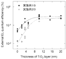
- FIG. 31 shows the relationship between the EL external quantum yield and the film thickness of the TiO 2 layer in the EL devices obtained in Examples 19 and 20.
- the EL external quantum efficiency is increased as the thickness of the TiO 2 layer is increased, and the behavior of saturation at a thickness of 10 nm or more is observed.
- AFM atomic force microscope
- the difference in height of the ITO cathode film itself is about 2 nm, whereas in the case of a TiO 2 layer having a film thickness of 10 nm or less, the TiO 2 layer Since the height difference is about 8 nm, it can be seen that the TiO 2 layer is not completely covered with the ITO cathode and has a dot-like film quality. Therefore, when the TiO 2 layer is 8 nm or less, the hole blocking effect is insufficient. On the other hand, as shown in FIG. 32 (iii), the difference in height of the TiO 2 film does not increase even when the film thickness is 10 nm or more, and maintains a substantially constant value of about 8 nm.
- Blue-green light emission derived from EHPy was observed from the whole area. 30 minutes after the dropping, the liquid light emitting material is in the state shown in FIG. 33 (v). When a voltage of 170V is applied between the two ITO electrodes, the ITO electrodes cross as shown in FIG. 33 (ix). Blue-green light emission derived from EHPy was observed from the whole area. As described above, it can be seen that electroluminescence is observed while the liquid luminescent material always moves between the electrodes.
- Example 22 A liquid luminescent material consisting of 83.1 parts by mass of EHCz, 16.6 parts by mass of guest compound 2 and 0.3 parts by mass of TBAPF 6 was injected into an ITO cell (manufactured by EHC) having a 10 ⁇ m gap similar to Example 21. .
- EHC electronic vapor deposition
- FIG. 38 (i) shows the state shown in FIG. 38 (i) at that time.
- FIG. 38 (ii) shows a state in which the liquid light emitting material is deteriorated until light emission of the guest compound 2 disappears after 5 minutes from the voltage application. Even in the PL emission of FIG.
- FIG. 38 (v) a decrease in emission intensity due to deterioration can be confirmed in the portion in contact with ITO.
- FIG. 38 (iii) shows a state in which a new liquid light-emitting material is injected using the capillary phenomenon after the liquid light-emitting material is deteriorated and a voltage of 170 V is applied. This indicates that the light emission of the element is restored by replacing the deteriorated light emitting material with a new liquid light emitting material. Further, in the PL light emission of FIG. 38 (vi), it can be confirmed that the deteriorated light emitting material flows and is replaced with a new light emitting material. As described above, the element can be restored by injecting a new liquid light emitting material even after the liquid light emitting material has deteriorated.
- Example 23 Electroluminescence upon application of AC voltage
- An EL device was produced in the same manner as in Example 1 except that a liquid light-emitting material composed of 99.75 parts by mass of EHPy and 0.25 parts by mass of tributyl (2-methoxyethyl) phosphonium bis (trifluoromethanesulfonyl) imide was used.
- the film thickness of the liquid light emitting layer of this device was calculated from the results of dielectric constant measurement, and was 1.20 ⁇ 0.06 ⁇ m.
- the luminance-voltage characteristics of the fabricated EL element when direct current and alternating voltage were applied were measured. The results are shown in FIG. As shown in FIG.
Landscapes
- Physics & Mathematics (AREA)
- Optics & Photonics (AREA)
- Chemical & Material Sciences (AREA)
- Engineering & Computer Science (AREA)
- Materials Engineering (AREA)
- Spectroscopy & Molecular Physics (AREA)
- Manufacturing & Machinery (AREA)
- Crystallography & Structural Chemistry (AREA)
- Inorganic Chemistry (AREA)
- Electroluminescent Light Sources (AREA)
Abstract
Description
この有機EL素子は、発光性有機化合物を発光層に用いた発光素子であるため、軽量かつフレキシブル、そして安価で大面積のフルカラー表示が可能なディスプレイとして応用が期待されている。
そのため、発光層には、これら3つの機能を満たす材料が必要不可欠であり、通常、その材料としては、これら3つの機能を発揮するキャリア輸送性発光材料や、3つの機能を補うために複数種の有機物を混合させたキャリア輸送材料/発光材料が用いられている。
ところで、発光層用の発光材料には、単純に目的の蛍光波長および高い量子収率を持つものを用いればよいというわけではなく、特定の蛍光色素に適したキャリア輸送材料の選定を行う必要がある。この理由は、キャリア輸送材料中に輸送されたキャリアが再結合し、そこで生じる励起エネルギーがキャリア輸送材料中にドープされている蛍光色素の発光を誘起するためである。
そのため、発光材料/キャリア輸送材料の各成分のHOMO/LUMOのエネルギー準位の相互関係、あるいは、それらの効率的なエネルギー移動の組み合せの選定が、デバイスの駆動や発光効率の向上に努めるために必要不可欠な課題となってくる。
これは、1987年、Kodak社のTangらによって報告された機能性分離薄膜積層型有機EL素子(以下、薄膜積層型有機EL素子)を起源とし、現在においては、陰極/電子注入層/電子輸送層/正孔ブロック層/発光層/電子ブロック層/正孔輸送層/正孔注入層/陽極等の各機能を有する材料を幾層にも張り合わせた薄膜積層型有機EL素子の開発が進められてきている。
また、薄膜積層型有機EL素子とは別の手法として、非特許文献1に開示されているような、高分子発光材料中に有機塩を添加して、キャリアの注入効率を向上させることで、低駆動電圧および高輝度の発光素子が得られることが報告されている。
この劣化を防ぐためには、電極表面の水分、酸素や、構成する有機薄膜に含まれる僅かな不純物等の除去が必要となる。
その具体的な手法としては、有機EL素子を構成する有機物の純度および安定性の向上や、外部からの酸素および水分の混入を防ぐために乾燥剤等を封止する方法が利用されている。
上述した既存の有機EL素子は、これら各有機層の焼付けが素子の劣化の原因になっており、有機EL素子を構成する複数ある有機層のうち一層でも劣化すれば、素子全体の寿命に大きく影響する。
仮に、この劣化した有機層を、例えばカートリッジ等により、交換可能な構造とすれば、新たな有機層を供給し続けることができる結果、有機EL素子を半永久的に駆動できると考えられる。
しかし、上述した既存の有機EL素子のほとんどは、固体の有機薄膜が用いられており、劣化した有機層のみを交換することは非常に困難である。
しかし、非特許文献2に開示されている、発光層を液状化した有機EL素子は、既存の照明やディスプレイに置き換え可能なほどの高い特性を示す有機EL素子とは言い難く、その液体発光層やデバイス構造は、最適化が必要である。
また、非特許文献1における素子構造は、陰極/発光層/正孔注入層/陽極と比較的単純なものとされているが、上述したように高い有機EL特性を向上させるためには、薄膜積層型有機EL構造へと改良する余地が残っている。
そこで、本発明者らは、液状発光層を備えた有機EL素子のEL特性の更なる向上を図るべく鋭意検討を重ねた結果、発光層にイオン性材料を添加することで、より高輝度、低駆動電圧、高発光効率を有する有機電界発光素子(有機EL素子)が得られることを見出し、本発明を完成した。
1. 陽極と、陰極と、これら各極間に介在する、常温で液体の発光層とを備え、前記発光層が、イオン性材料を含むことを特徴とする有機電界発光素子、
2. 前記発光層が、キャリア輸送能および発光能を有する材料と、イオン性材料とから構成される1の有機電界発光素子、
3. 前記発光層が、キャリア輸送材料と、発光材料と、イオン性材料とから構成される1の有機電界発光素子、
4. 前記イオン性材料が、液状の有機塩、液状の無機塩、液状のキャリア輸送材料または液状の発光材料に分散可能な有機塩、および液状のキャリア輸送材料または液状の発光材料に分散可能な無機塩から選ばれる1種または2種以上である3の有機電界発光素子、
5. 前記イオン性材料が、式[1]で示される化合物を含む1~4のいずれかの有機電界発光素子、
(An+)i(Bm-)j [1]
〔式中、An+は、n(nは1~10の整数を表す)価のカチオン成分であって、金属イオン、または窒素原子、リン原子、硫黄原子もしくは酸素原子を含むオニウムイオンを表し、Bm-は、m(mは1~10の整数を表す)価のアニオン成分であって、ハロゲン化物イオン、オキソ酸アニオン、ホウ素原子を含むアニオン、リン原子を含むアニオン、イミド系アニオンを表す。iおよびjは、それぞれ1~100の整数、かつ、式[1]で表されるイオン性材料が電気的中性となる整数である。〕
6. 前記イオン性材料が、発光層中に、0.01~50質量%含まれる1~5のいずれかの有機電界発光素子、
7. 前記発光層を含む少なくとも3層の機能層を備える機能分離型薄膜構造を有する1~6のいずれかの有機電界発光素子、
8. 前記機能層として、前記陰極および発光層の間に介在するホールブロック層を有する1~7のいずれかの有機電界発光素子、
9. 前記ホールブロック層が、金属酸化物、金属窒化物、金属硫化物、金属酸化窒化物、高分子化合物を含む8の有機電界発光素子、
10. 前記ホールブロック層が、Ti,Zr,Ba,Ca,Sr,Yb,Al,Ga,In,Li,Na,Cd,Mg,Si,TaおよびSbから選ばれる金属元素を少なくとも1種含む、酸化物、窒化物、硫化物および酸化窒化物から選ばれる1種または2種以上を含む9の有機電界発光素子
を提供する。
この有機電界発光素子は、駆動時および非駆動時ともに発光層が液状を維持し得る。このため、発光層が劣化した場合に、発光層のみを交換する構成(例えば、カートリッジ、循環による抜き出し・再注入)とすることも可能である。
また、発光層が液体であることから、塗布プロセスを用いて素子を製造することができるため、大面積の照明素子にも応用可能である。
さらに、既存の固体の有機薄膜からなる有機EL素子よりも、フレキシビリティーの高い表示素子の作製も可能になる。
本発明に係る有機電界発光素子は、陽極と、陰極と、これら各極間に介在する、常温で液体の発光層とを備え、この発光層が、イオン性材料を含むものである。
ここで、常温とは、JIS Z 8703で規定されている、20℃±15℃(5~35℃)の範囲を意味する。
なお、物質によっては、キャリア輸送能および発光能の両機能を明確に分離できず、例えば、カルバゾール、トリアリールアミン、炭素縮合環系色素等の中には、両機能を併せ持つものも存在する。
本発明では、発光層全体として液体の性状を示す限りにおいて、このような両機能を併せ持つ物質を用いることができ、また、液状を示すものであれば、それ単独で用いることもできる。

これらの中でも、優れた正孔輸送性能を有するという点から、カルバゾールが好ましい。
この場合、アルキル基は、直鎖、分岐、環状のいずれでもよいが、直鎖状のアルキル基を用いた場合、アルキル鎖同士のパッキング等の分子間相互作用により、結晶性の向上や粘度の増加が考えられるため、分岐状のアルキル基がより好ましい。
このような炭素数1~30のアルキル基の具体例としては、メチル、エチル、n-プロピル、i-プロピル、c-プロピル、n-ブチル、i-ブチル、s-ブチル、t-ブチル、c-ブチル、n-ペンチル、1-メチル-n-ブチル、2-メチル-n-ブチル、3-メチル-n-ブチル、1,1-ジメチル-n-プロピル、c-ペンチル、2-メチル-c-ブチル、n-ヘキシル、1-メチル-n-ペンチル、2-メチル-n-ペンチル、1,1-ジメチル-n-ブチル、1-エチル-n-ブチル、1,1,2-トリメチル-n-プロピル、c-ヘキシル、1-メチル-c-ペンチル、1-エチル-c-ブチル、1,2-ジメチル-c-ブチル、n-ヘプチル、n-オクチル、2-エチルヘキシル、n-ノニル、n-デシル、n-ウンデシル、n-ドデシル、n-トリデシル、n-テトラデシル、n-ペンタデシル、n-ヘキサデシル、n-ヘプタデシル、n-オクタデシル、n-ノナデシル、n-エイコシル基等が挙げられる。
本発明においては、特に、エーテル結合を含む炭素数1~30のアルキル基を採用することで、イオン性材料をよく溶かすキャリア輸送材料とすることができる。
、CH2OC(CH3)2(CH2)2CH3、CH2OCH(CH2CH3)(CH2)2CH3、CH2OC(CH3)2CH(CH3)CH3、CH2O(CH2)6CH3、CH2O(CH2)7CH3、CH2OCH2CH(CH2CH3)(CH2)3CH3、CH2O(CH2)8CH3、CH2O(CH2)9CH3、CH2O(CH2)10CH3、CH2O(CH2)11CH3、CH2O(CH2)12CH3、CH2O(CH2)13CH3、CH2O(CH2)14CH3、CH2O(CH2)15CH3、CH2O(CH2)16CH3、CH2O(CH2)17CH3、CH2O(CH2)18CH3、CH2O(CH2)19CH3、CH2CH2OCH3、CH2CH2OCH2CH3、CH2CH2O(CH2)2CH3、CH2CH2OCH(CH3)2、CH2CH2O(CH2)3CH3、CH2CH2OCH2CH(CH3)2、CH2CH2OC(CH3)3、CH2CH2O(CH2)4CH3、CH2CH2OCH(CH3)(CH2)2CH3、CH2CH2OCH2CH(CH3)CH3、CH2CH2O(CH2)2CH(CH3)CH3、CH2CH2OC(CH3)2CH3、CH2CH2OCH(CH3)(CH2)3CH3、CH2CH2O(CH2)5CH3、CH2CH2OCH(CH3)(CH2)3CH3、CH2CH2OCH2CH(CH3)(CH2)2CH3、CH2CH2O(CH2)2CH(CH3)CH2CH3、CH2CH2O(CH2)3CH(CH3)CH3、CH2CH2OC(CH3)2(CH2)2CH3、CH2CH2OCH(CH2CH3)(CH2)2CH3、CH2CH2OC(CH3)2CH(CH3)CH3、CH2CH2O(CH2)6CH3、CH2CH2O(CH2)7CH3、CH2CH2OCH2CH(CH2CH3)(CH2)3CH3、CH2CH2O(CH2)8CH3、CH2CH2O(CH2)9CH3、CH2CH2O(CH2)10CH3、CH2CH2O(CH2)11CH3、CH2CH2O(CH2)12CH3、CH2CH2O(CH2)13CH3、CH2CH2O(CH2)14CH3、CH2CH2O(CH2)15CH3、CH2CH2O(CH2)16CH3、CH2CH2O(CH2)17CH3、CH2CH2O(CH2)18CH3、CH2CH2O(CH2)19CH3、CH2CH2CH2OCH3、CH2CH2CH2OCH2CH3、CH2CH2CH2O(CH2)2CH3、CH2CH2CH2OCH(CH3)2、CH2CH2CH2O(CH2)3CH3、CH2CH2CH2OCH2CH(CH3)2、CH2CH2CH2OC(CH3)3、CH2CH2CH2O(CH2)4CH3、CH2CH2CH2OCH(CH3)(CH2)2CH3、CH2CH2CH2OCH2CH(CH3)CH3、CH2CH2CH2O(CH2)2CH(CH3)CH3、CH2CH2CH2OC(CH3)2CH3、CH2CH2CH2OCH(CH3)(CH2)3CH3、CH2CH2CH2O(CH2)5CH3、CH2CH2CH2OCH(CH3)(CH2)3CH3、CH2CH2CH2OCH2CH(CH3)(CH2)2CH3、CH2CH2CH2O(CH2)2CH(CH3)CH2CH3、CH2CH2CH2O(CH2)3CH(CH3)CH3、CH2CH2CH2OC(CH3)2(CH2)2CH3、CH2CH2CH2OCH(CH2CH3)(CH2)2CH3、CH2CH2CH2OC(CH3)2CH(CH3)CH3、CH2CH2CH2O(CH2)6CH3、CH2CH2CH2O(CH2)7CH3、CH2CH2CH2OCH2CH(CH2CH3)(CH2)3CH3、CH2CH2CH2O(CH2)8CH3、CH2CH2CH2O(CH2)9CH3、CH2CH2CH2O(CH2)10CH3、CH2CH2CH2O(CH2)11CH3、CH2CH2CH2O(CH2)12CH3、CH2CH2CH2O(CH2)13CH3、CH2CH2CH2O(CH2)14CH3、CH2CH2CH2O(CH2)15CH3、CH2CH2CH2O(CH2)16CH3、CH2CH2CH2O(CH2)17CH3、CH2CH2CH2O(CH2)18CH3、CH2CH2CH2O(CH2)19CH3、CH2CH2OCH2CH2OCH3、CH2CH2OCH2CH2OCH2CH2OCH3、CH2CH2OCH2CH2OCH2CH2OCH2CH2OCH3、CH2CH2OCH2CH2OCH2CH2OCH2CH2OCH2CH2OCH3、CH2CH2OCH2CH2OCH2CH2OCH2CH2OCH2CH2OCH2CH2OCH3、CH2CH2OCH2CH2OCH2CH2OCH2CH2OCH2CH2OCH2CH2OCH2CH2OCH3、CH2CH2OCH2CH2OCH2CH2OCH2CH2OCH2CH2OCH2CH2OCH2CH2OCH2CH2OCH3、CH2CH2CH2OCH2CH2CH2OCH3、
CH2CH2CH2OCH2CH2CH2OCH2CH2CH2OCH3、CH2CH2CH2OCH2CH2CH2OCH2CH2CH2OCH2CH2CH2OCH3、CH2CH2CH2OCH2CH2CH2OCH2CH2CH2OCH2CH2CH2OCH2CH2CH2OCH3、CH2CH2CH2OCH2CH2CH2OCH2CH2CH2OCH2CH2CH2OCH2CH2CH2OCH2CH2CH2OCH3、CH2CH2CH2OCH2CH2CH2OCH2CH2CH2OCH2CH2CH2OCH2CH2CH2OCH2CH2CH2OCH2CH2CH2OCH3、CH2CH2CH2OCH2CH2CH2OCH2CH2CH2OCH2CH2CH2OCH2CH2CH2OCH2CH2CH2OCH2CH2CH2OCH2CH2CH2OCH3、CH2CH2CH2CH2OCH2CH2CH2CH2OCH3、CH2CH2CH2CH2OCH2CH2CH2CH2OCH2CH2CH2CH2OCH3、CH2CH2CH2CH2OCH2CH2CH2CH2OCH2CH2CH2CH2OCH2CH2CH2CH2OCH3、CH2CH2CH2CH2OCH2CH2CH2CH2OCH2CH2CH2CH2OCH2CH2CH2CH2OCH2CH2CH2CH2OCH3、CH2CH2CH2CH2OCH2CH2CH2CH2OCH2CH2CH2CH2OCH2CH2CH2CH2OCH2CH2CH2CH2OCH2CH2CH2CH2OCH3、CH2CH2CH2CH2OCH2CH2CH2CH2OCH2CH2CH2CH2OCH2CH2CH2CH2OCH2CH2CH2CH2OCH2CH2CH2CH2OCH2CH2CH2CH2OCH3、CH2CH2OCH2CH2OCH2CH3、CH2CH2OCH2CH2OCH2CH2OCH2CH3、CH2CH2OCH2CH2OCH2CH2OCH2CH2OCH2CH3、CH2CH2OCH2CH2OCH2CH2OCH2CH2OCH2CH2OCH2CH3、CH2CH2OCH2CH2OCH2CH2OCH2CH2OCH2CH2OCH2CH2OCH2CH3、CH2CH2OCH2CH2OCH2CH2OCH2CH2OCH2CH2OCH2CH2OCH2CH2OCH2CH3、CH2CH2OCH2CH2OCH2CH2OCH2CH2OCH2CH2OCH2CH2OCH2CH2OCH2CH2OCH2CH3基等や、下記式で示される基などが挙げられる。

エステル結合を含んでいる上記アルキル基の具体例としては、上記エーテル結合を含んでいるアルキル基の酸素原子(O)を、C(O)OまたはOC(O)に代えた基等が挙げられる。
炭酸エステル結合を含んでいる上記アルキル基の具体例としては、上記エーテル結合を含んでいるアルキル基の酸素原子(O)を、OC(O)Oに代えた基等が挙げられる。
アミド結合を含んでいる炭素数1~30のアルキル基の具体例としては、上記エーテル結合を含んでいるアルキル基の酸素原子(O)を、C(O)NHまたはNHC(O)に代えた基等が挙げられる。
CH2O(CH2)18CH3、CH2O(CH2)19CH3、CH2CH2O(CH2)5CH3、CH2CH2OCH(CH3)(CH2)3CH3、CH2CH2OCH2CH(CH3)(CH2)2CH3、CH2CH2O(CH2)2CH(CH3)CH2CH3、CH2CH2O(CH2)3CH(CH3)CH3、CH2CH2OC(CH3)2(CH2)2CH3、CH2CH2OCH(CH2CH3)(CH2)2CH3、CH2CH2OC(CH3)2CH(CH3)CH3、CH2CH2O(CH2)6CH3、CH2CH2O(CH2)7CH3、CH2CH2OCH2CH(CH2CH3)(CH2)3CH3、CH2CH2O(CH2)8CH3、CH2CH2O(CH2)9CH3、CH2CH2O(CH2)10CH3、CH2CH2O(CH2)11CH3、CH2CH2O(CH2)12CH3、CH2CH2O(CH2)13CH3、CH2CH2O(CH2)14CH3、CH2CH2O(CH2)15CH3、CH2CH2O(CH2)16CH3、CH2CH2O(CH2)17CH3、CH2CH2O(CH2)18CH3、CH2CH2O(CH2)19CH3、CH2CH2CH2O(CH2)5CH3、CH2CH2CH2OCH(CH3)(CH2)3CH3、CH2CH2CH2OCH2CH(CH3)(CH2)2CH3、CH2CH2CH2O(CH2)2CH(CH3)CH2CH3、CH2CH2CH2O(CH2)3CH(CH3)CH3、CH2CH2CH2OC(CH3)2(CH2)2CH3、CH2CH2CH2OCH(CH2CH3)(CH2)2CH3、CH2CH2CH2OC(CH3)2CH(CH3)CH3、CH2CH2CH2O(CH2)6CH3、CH2CH2CH2O(CH2)7CH3、CH2CH2CH2OCH2CH(CH2CH3)(CH2)3CH3、CH2CH2CH2O(CH2)8CH3、CH2CH2CH2O(CH2)9CH3、CH2CH2CH2O(CH2)10CH3、CH2CH2CH2O(CH2)11CH3、CH2CH2CH2O(CH2)12CH3、CH2CH2CH2O(CH2)13CH3、CH2CH2CH2O(CH2)14CH3、CH2CH2CH2O(CH2)15CH3、CH2CH2CH2O(CH2)16CH3、CH2CH2CH2O(CH2)17CH3、CH2CH2CH2O(CH2)18CH3、CH2CH2CH2O(CH2)19CH3、CH2CH2OCH2CH2OCH3、CH2CH2OCH2CH2OCH2CH2OCH3、CH2CH2OCH2CH2OCH2CH2OCH2CH2OCH3、CH2CH2OCH2CH2OCH2CH2OCH2CH2OCH2CH2OCH3、CH2CH2OCH2CH2OCH2CH2OCH2CH2OCH2CH2OCH2CH2OCH3、CH2CH2OCH2CH2OCH2CH2OCH2CH2OCH2CH2OCH2CH2OCH2CH2OCH3、CH2CH2OCH2CH2OCH2CH2OCH2CH2OCH2CH2OCH2CH2OCH2CH2OCH2CH2OCH3、CH2CH2CH2OCH2CH2CH2OCH3、CH2CH2CH2OCH2CH2CH2OCH2CH2CH2OCH3、CH2CH2CH2OCH2CH2CH2OCH2CH2CH2OCH2CH2CH2OCH3、CH2CH2CH2OCH2CH2CH2OCH2CH2CH2OCH2CH2CH2OCH2CH2CH2OCH3、CH2CH2CH2OCH2CH2CH2OCH2CH2CH2OCH2CH2CH2OCH2CH2CH2OCH2CH2CH2OCH3、CH2CH2CH2OCH2CH2CH2OCH2CH2CH2OCH2CH2CH2OCH2CH2CH2OCH2CH2CH2OCH2CH2CH2OCH3、CH2CH2CH2OCH2CH2CH2OCH2CH2CH2OCH2CH2CH2OCH2CH2CH2OCH2CH2CH2OCH2CH2CH2OCH2CH2CH2OCH3、CH2CH2OCH2CH2OCH2CH3、CH2CH2OCH2CH2OCH2CH2OCH2CH3、CH2CH2OCH2CH2OCH2CH2OCH2CH2OCH2CH3、CH2CH2OCH2CH2OCH2CH2OCH2CH2OCH2CH2OCH2CH3、CH2CH2OCH2CH2OCH2CH2OCH2CH2OCH2CH2OCH2CH2OCH2CH3、CH2CH2OCH2CH2OCH2CH2OCH2CH2OCH2CH2OCH2CH2OCH2CH2OCH2CH3、CH2CH2OCH2CH2OCH2CH2OCH2CH2OCH2CH2OCH2CH2OCH2CH2OCH2CH2OCH2CH3基等、並びにこれらの基の酸素原子(O)を、硫黄原子(S)に代えた基、C(O)OまたはOC(O)に代えた基、OC(O)Oに代えた基、およびC(O)NHまたはNHC(O)に代えた基等が好適である。
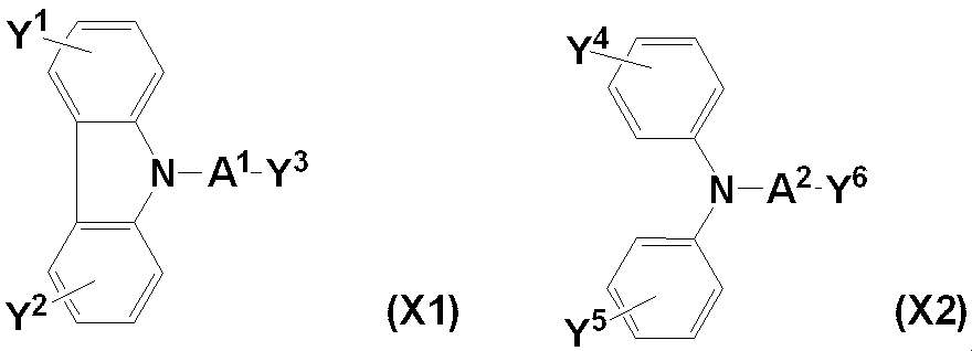
ここで、‘アルキル基’という用語は、メチル、エチル、イソプロピル、t-ブチル、2-エチルヘキシル、シクロヘキシルのような線状、分岐型、環状アルキルを含み、これは上記一般式(1)の融点を降下させる官能基(Y)に相当し、その具体例および好適例は上述のとおりである。
芳香族環としては、ベンゼン環、ナフタレン環等が挙げられる。
これらの点から、下記化合物(X3)が好ましく、化合物(3)がより好ましく、化合物(4)または化合物(5)がより一層好ましいが、これらに限定されるものではない。

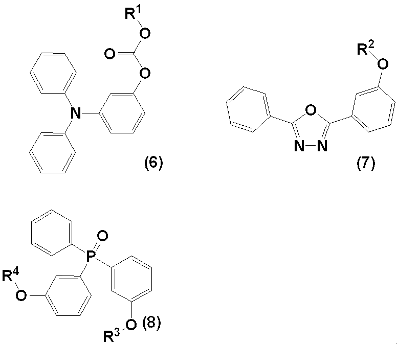

このような、キャリア輸送材料としては、従来公知の材料から適宜選択すればよく、例えば、(トリフェニルアミン)ダイマー誘導体(TPD)、(α-ナフチルジフェニルアミン)ダイマー(α-NPD)、[(トリフェニルアミン)ダイマー]スピロダイマー(Spiro-TAD)等のトリアリールアミン類、4,4’,4”-トリス[3-メチルフェニル(フェニル)アミノ]トリフェニルアミン(m-MTDATA)、4,4’,4”-トリス[1-ナフチル(フェニル)アミノ]トリフェニルアミン(1-TNATA)等のスターバーストアミン類;5,5”-ビス-{4-[ビス(4-メチルフェニル)アミノ]フェニル}-2,2’:5’,2”ターチオフェン(BMA-3T)等のオリゴチオフェン類、ポリビニルカルバゾール類などの正孔輸送材料;Alq3、BAlq、DPVBi、(2-(4-ビフェニル)-5-(4-t-ブチルフェニル)-1,3,4-オキサジアゾール)(PBD)、トリアゾール誘導体(TAZ)、バソクプロイン(BCP)、シロール誘導体などの電子輸送材料が挙げられる。
これらの中でも、発光効率に優れるという点から、ルブレン誘導体が好ましい。

上記色素部およびアルキル基の具体例としては、上記と同様のものが挙げられる。
具体的な発光材料としては、例えば、発光特性に優れる炭素縮合環系色素である、下記ピレン誘導体(Z1)が挙げられる。

これらの点から、下記化合物(Z3)が好ましいが、これに限定されるものではない。
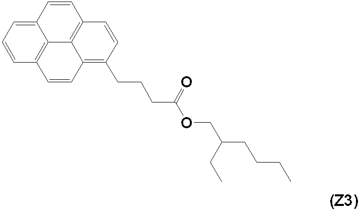
このような、発光材料としては、従来公知の材料から適宜選択すればよく、例えば、トリス(8-キノリノラート)アルミニウム(III)(Alq3)、ビス(8-キノリノラート)亜鉛(II)(Znq2)、ビス(2-メチル-8-キノリノラート)(p-フェニルフェノラート)アルミニウム(III)(BAlq)、4,4’-ビス(2,2-ジフェニルビニル)ビフェニル(DPVBi)等が挙げられる。
その具体例としては、下記式[1]で示される化合物が挙げられる。
(An+)i(Bm-)j [1]
上記式中、An+は、n(nは1~10の整数を表す)価のカチオン成分であって、金属イオン、または窒素原子、リン原子、硫黄原子もしくは酸素原子を含むオニウムイオンを表し、Bm-は、m(mは1~10の整数を表す)価のアニオン成分であって、ハロゲン化物イオン、オキソ酸アニオン、ホウ素原子を含むアニオン、リン原子を含むアニオン、イミド系アニオンを表す。iおよびjは、それぞれ1~100の整数、かつ、式[1]で表されるイオン性材料が電気的中性となる整数である。
リン原子を含むオニウムイオンとしては、テトラメチルホスホニウムカチオン、テトラエチルホスホニウムカチオン、テトラ(n-ブチル)ホスホニウムカチオン等のテトラアルキルホスホニウムカチオン;PH4 +などが挙げられる。
硫黄原子を含むオニウムイオンとしては、トリメチルスルホニウムカチオン、トリエチルスルホニウムカチオン、トリ(n-ブチル)スルホニウムカチオン等のトリアルキルスルホニウムカチオンなどが挙げられる。
酸素原子を含むオニウムイオンとしては、トリメチルオキソニウムカチオン、トリエチルオキソニウムカチオン、トリ(n-ブチル)オキソニウムカチオン等のトリアルキルオキソニウムカチオンなどが挙げられる。
オキソ酸アニオンとしては、ホウ酸アニオン、炭酸アニオン、酢酸アニオン、硫酸アニオン、リン酸アニオンなどが挙げられる。
ホウ素原子を含むアニオンとしては、BF4 -;テトラメチルボレート、テトラエチルボレート等のテトラアルキルボレート;テトラフェニルボレート、テトラキス(ペンタフルオロフェニル)ボレート等のテトラアリールボレートなどが挙げられる。
リン原子を含むアニオンとしては、PF6 -などが挙げられる。
イミド系アニオンとしては、ビス(トリフルオロメタンスルホニル)イミドアニオン等のビス(パーフルオロアルカンスルホニル)イミドアニオンなどが挙げられる。
発光材料やキャリア輸送材料と、イオン性材料とを混合する手法は任意であるが、固体の成分を使用する場合、液体成分に固体成分を混合する手法が好適である。
例えば、陽極材料としては、インジウム錫酸化物(ITO)、インジウム亜鉛酸化物(IZO)に代表される透明電極や、高電荷輸送性を有するポリチオフェン誘導体、ポリアニリン誘導体などを用いることができる。
陰極材料としては、アルミニウム、マグネシウム-銀合金、アルミニウム-リチウム合金、リチウム、ナトリウム、カリウム、セシウム、セシウム添加ITOなどを用いることができる。
このような機能層としては、正孔輸送層、正孔注入層、電子輸送層、電子注入層、キャリアブロック層(ホールブロック層、電子ブロック層)などが挙げられる。
また、正孔注入層は、正孔輸送層と陽極との間に設けられ、陽極からの正孔注入効率を高める機能を有する層である。
正孔注入層を形成する材料としては、銅フタロシアニン、4,4’,4”-トリス[3-メチルフェニル(フェニル)アミノ]トリフェニルアミン(m-MTDATA)等が挙げられる。
電子注入層は、電子輸送層と陰極との間に設けられ、陰極からの電子注入効率を高める機能を有する層である。
このような電子注入層を形成する材料としては、酸化リチウム(Li2O)、酸化マグネシウム(MgO)、アルミナ(Al2O3)、フッ化リチウム(LiF)、フッ化マグネシウム(MgF2)、フッ化ストロンチウム(SrF2)、Li(acac)、酢酸リチウム、安息香酸リチウム等が挙げられる。
このホールブロック層に使用可能な材料は、液状発光層からの正孔の移動を阻害でき、さらに液状発光層に不溶な電子輸送性材料であれば特に限定されることはなく、一般的にホールブロック層に用いられる、金属酸化物、金属窒化物、金属硫化物、金属酸化窒化物、高分子化合物から選ばれる1種または2種以上が好ましい。
金属酸化物、金属窒化物、金属硫化物、金属酸化窒化物としては、例えば、Ti,Zr,Ba,Ca,Sr,Yb,Al,Ga,In,Li,Na,Cd,Mg,Si,TaおよびSbから選ばれる金属元素を少なくとも1種含む、酸化物、窒化物、硫化物および酸化窒化物が挙げられ、これらの中でも、酸化チタン、酸化ジルコニウム、硫化亜鉛、硫化カドミウム等がより好ましい。
高分子化合物としては、例えば、アニリン系共重合体、オリゴまたはポリチオフェン、ポリチオフェン誘導体、ポリフェニレン誘導体、ポリフェニレンビニレン誘導体、ポリフルオレン誘導体などが挙げられる。
ホールブロック層の膜厚は、十分なホールブロック能を確保し、かつ駆動電圧の上昇を防ぐという観点から、1~1000nm程度が好ましく、より好ましくは5~50nm程度である。
図1には、本発明の一実施形態に係る電界発光素子である、有機EL素子1が示されている。
この有機EL素子1は、陽極10と、陽極10上に積層された正孔注入層30と、陰極20と、陰極20上に積層されたホールブロック層40と、これら正孔注入層30およびホールブロック層40間に介在する、常温で液体かつイオン性材料を含む発光層50(以下、液体発光層50という)とを備えている。
一方、陰極20は、ガラス基板13と、この上に成膜されたITO基板14とから構成されている。
また、ホールブロック層40は酸化チタンから構成され、正孔注入層30は、PEDOT:PSS膜から構成されている。
まず、陽極10上に、PEDOT:PSSをスピンコート法によって塗布し、これを加熱して正孔注入層30を成膜する。
一方、ガラス基板13およびITO基板14の積層体上に、酸化チタンをスパッタ法によって積層し、ホールブロック層40を成膜する。
続いて、陽極10(正孔注入層30)上に、ルブレンとTBAPF6を所定量含有する9-(2-エチルヘキシル)カルバゾール(EHCz)液を滴下して液体発光層50を形成し、その上にホールブロック層40を積層した陰極20を適切な圧力で押しつけて有機EL素子1を得る。
また、各層の成膜方法も上記実施形態の手法に限定されるものではなく、用いる材料に応じて、蒸着法、スプレー法、インクジェット法、スパッタリング法等の公知の手法を適宜採用することができる。
さらに、ホールブロック層や正孔注入層等は必要に応じて形成される層であり、例えば、図2に示されるように、ホールブロック層を有しない有機EL素子2のような構成を採用することもできる。
なお、実施例で用いた測定装置は以下のとおりである。
(1)電流-電圧-輝度特性
フォトディテクター付き半導体パラメーターアナライザー(アジレント社製、B1500A)と光パワー-メーター(ニューポート、1930C)によって計測した。
(2)EL発光スペクトル
マルチチャンネル分光器(PMA-11,浜松ホトニクス(株)製)によって計測した。
(3)1H-NMR
装置:AVANCE 500、Bruker社製
装置:JNM-LA400、日本電子データム(株)製
(4)マトリックス支援レーザー脱離イオン化飛行時間型質量分析
マトリックス支援レーザー脱離イオン化飛行時間型質量分析装置(MALDI-TOF-MS)、Autoflex-III.Bruker Daltonics社製
(5)原子間力顕微鏡(AFM)
装置:走査型プローブ顕微鏡(JSPM-5400,JEOL社製)
(6)交流電圧印加時の電圧-輝度特性
交流電源(エー・アンド・デー社製、SWEEP FUNCTION GENERATOR AD-8623)で発生させたシグナルを電圧増幅器(エヌエフコーポレーション社製、HIGH SPEED BIPOLAR AMPLIFIER 4101)で増幅し、EL素子に印加することで駆動させた。輝度は光パワー-メーター(ニューポート、1930C)で、電圧はオシロスコープ(アジレント社製、MSO6104A)で測定した。


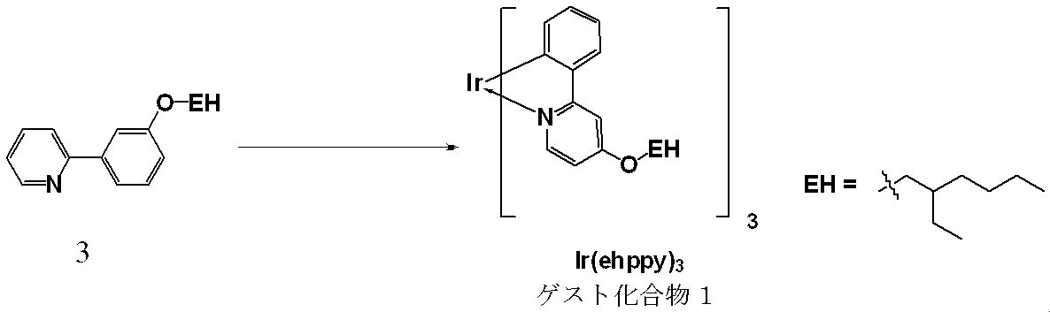
下記スキーム1,2に従って、ゲスト化合物2を合成した。ゲスト化合物2の1H-NMRスペクトルを図37に示す。
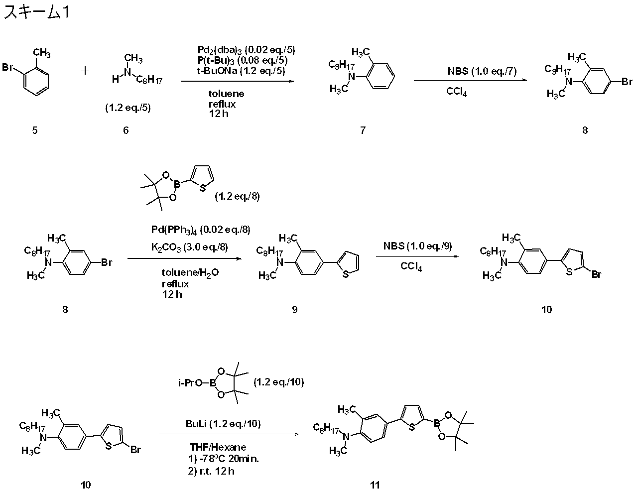
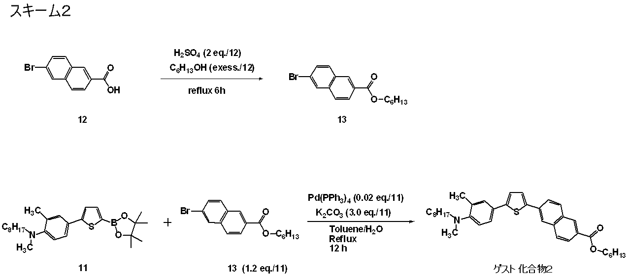
[実施例1]
室温で液体状のホスト化合物として9-(2-エチルヘキシル)カルバゾール(以下、EHCz)83.2質量部に、合成例3で得られたゲスト化合物2 16.7質量部、イオン性材料であるテトラブチルアンモニウムヘキサフルオロホスフェイト(以下、TBAPF6)0.1質量部を加え、ゲスト化合物2およびTBAPF6をEHCz中に完全に溶解させて液体発光材料を調製した。
界面活性剤、純水、イソプロパノールの順で超音波洗浄し、UV/オゾン処理(フィルゲン社製、UV253S)を12分間施したITOガラス基板を2枚用意した。
一方のITO12付きガラス基板11に、PEDOT:PSS(バイエル社製、PI4083)を3000rpmの回転数で30秒間スピンコートして成膜した後、200℃,10分間、大気中で加熱し、ホール注入層30がITO12上に成膜された陽極側基板10を得た。
次に、もう一方のITO14付きガラス基板13からなる陰極側基板20をグローブボックス中に入れ、先に調製した液体発光材料をITO14が成膜された側に少量滴下し、PEDOT:PSSが成膜されたITO陽極側基板10と挟みこみ、クリップ(図示省略)で固定することで、図2に示されるような、ガラス基板/ITO(陽極)/PEDOT:PSS40nm/液体発光層/ITO(陰極)/ガラス基板からなるEL素子2を作製した。素子面積は2mm×2mmである。
図3および図4に示されるように、発光は18.0Vから観測され、62.0V印加時に0.99mA/cm2の電流密度、2.3cd/m2の最大輝度、そして0.051%のEL外部量子効率が得られた。また、531nmに発光ピークを有する緑色の電界発光が得られた。
液体発光材料にTBAPF6を添加しない以外は実施例1と同様にEL素子を作製し、同様の評価を行った。結果を図3,4に示す。
このデバイスの液体発光層の膜厚を誘電率測定の結果から算出したところ1100nmであった。図3および4に示されるように、発光は34.1Vから観測され、79V印加時に0.95mA/cm2の電流密度、0.015cd/m2の最大輝度、0.00034%のEL外部量子効率が得られ、実施例1と同様に531nmに発光ピークを有する緑色発光が得られた。
EHCz98.9質量部に、ゲスト化合物として5,6,11,12-テトラフェニルナフタセン(以下、ルブレン)1.0質量部、TBAPF60.1質量部加え、ルブレンおよびTBAPF6をEHCz中に完全に溶解させることで液体発光材料を作製した。
上記液体発光材料を用いた以外は、実施例1と同様にEL素子を作製し、同様の評価を行った。結果を図5および図6に示す。このデバイスの液体発光層の膜厚を誘電率測定の結果から算出したところ380nmであった。
図5および図6に示されるように、発光は6.6Vから観測され、15.0V印加時に0.11mA/cm2の電流密度、0.034cd/m2の最大輝度、0.014%のEL外部量子効率が得られ、557nmの発光ピークを有するオレンジ色発光が得られた。
液体発光材料にTBAPF6を添加しない以外は実施例2と同様にEL素子を作製し、同様に評価を行った。結果を図5,6に示す。このデバイスの液体発光層の膜厚を誘電率測定の結果から算出したところ530nmであった。
図5および図6に示されるように、発光は40.1Vから観測され、93.2V印加時に0.21mA/cm2の電流密度、0.023cd/m2の最大輝度、0.0048%のEL外部量子効率が得られ、実施例2と同様に557nmの発光ピークを有するオレンジ色発光が得られた。
[実施例3]
液体発光材料にゲスト化合物1を添加しない以外は実施例1と同様にEL素子を作製し、同様の評価を行った。結果を図7および図8に示す。このデバイスの液体発光層の膜厚を誘電率測定の結果から算出したところ800nmであった。
図7および図8に示されるように、このデバイスでは、発光は15.8Vから観測され、80.6V印加時に1.5mA/cm2の電流密度と0.13cd/m2の最大輝度、71.4V印加時に0.96mA/cm2の電流密度と0.017%のEL外部量子効率が得られ、476nmに発光ピークを有する青色発光が得られた。
液体発光材料にTBAPF6を添加しない以外は実施例3と同様にEL素子を作製し、同様の評価を行った。このデバイスの液体発光層の膜厚を誘電率測定の結果から算出したところ900nmであった。図7に示されるように、このデバイスでは、100V印加時に0.11mA/cm2の電流密度を得たが、発光は観測されなかった。
合成例1で得られた液状ホスト化合物EHPy99.9質量部およびTBAPF60.1質量部からなる液体発光材料を用いた以外は、実施例1と同様にEL素子を作製し、同様の評価を行った。結果を図9および図10に示す。このデバイスの液体発光層の膜厚を誘電率測定の結果から算出したところ1150nmであった。
図9および図10に示されるように、発光は18.4Vから観測され、64.4V印加時に146mA/cm2の電流密度、416cd/m2の最大輝度、46.8V印加時に2.9mA/cm2の電流密度と0.13%の最大のEL外部量子効率が得られ、486nmにピークを有する青緑色の電界発光が得られた。
TBAPF6を添加しない以外は実施例4と同様にEL素子を作製し、同様の評価を行った。結果を図9および図10に示す。このデバイスの液体発光層の膜厚を誘電率測定の結果から算出したところ690nmであった。
図9および図10に示されるように、電界発光は60.8Vから観測され、100V印加時に0.067mA/cm2の電流密度と0.58cd/m2の最大輝度、0.23%のEL外部量子効率が得られ、実施例4と同様に486nmに発光ピークを有する青緑色の電界発光が得られた。
[実施例5]
ホスト化合物として合成例1で得られたEHCz92.7質量部、ゲスト化合物として合成例2で得られたIr(ehppy)3(ゲスト化合物1)7.2質量部、およびTBAPF60.1質量部からなる液体発光材料を用いた以外は実施例1と同様にEL素子を作製し、同様の評価を行った。結果を図11および図12に示す。このデバイスの液体発光層の膜厚を誘電率測定の結果から算出したところ1230nmであった。
図11および図12に示されるように、発光は44.8Vから観測され、93.6V印加時に1.3mA/cm2の電流密度、2.9cd/m2の最大輝度、0.052%の最大のEL外部量子効率が得られ、559nmに発光ピークを有するオレンジ色の電界発光が得られた。
TBAPF6を添加しない以外は実施例5と同様にEL素子を作製し、同様の評価を行った。このデバイスの液体発光層の膜厚を誘電率測定の結果から算出したところ930nmであった。このデバイスからは、図11に示されるように、100V印加時に0.19mA/cm2の電流密度を得たが、発光は観測されなかった。
[実施例6]
ホスト化合物として下記式で示されるCz-TEG89.9質量部、ゲスト化合物として下記式で示されるゲスト化合物3(アメリカンダイソース社製)10.0質量部およびTBAPF60.1質量部からなる液体発光材料を用いた以外は実施例1と同様にEL素子を作製し、同様の評価を行った。結果を図13および図14に示す。このデバイスの液体発光層の膜厚を誘電率測定の結果から算出したところ1090nmであった。
図13および図14に示されるように、発光は16.0Vから観測され、40.0V印加時に0.52mA/cm2の電流密度、0.25cd/m2の最大輝度、0.074%のEL外部量子効率が得られ、419nmに発光ピークを有する青色の発光が得られた。
なお、Cz-TEGはSynthetic Metals,89(3),171(1997)に記載の方法を参考に合成した。
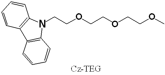

Cz-TEG69.9質量部、ゲスト化合物として下記式で示されるゲスト化合物4(アメリカンダイソース社製)30.0質量部、TBAPF60.1質量部からなる液体発光材料を用いた以外は実施例1と同様にEL素子を作製し、同様の評価を行った。結果を図15および図16に示す。
このデバイスの液体発光層の膜厚を誘電率測定の結果から算出したところ1090nmであった。図15および図16に示されるように、発光は15.8Vから観測され、40.0V印加時に0.17mA/cm2の電流密度、0.83cd/m2の最大輝度、0.24%のEL外部量子効率が得られ、470nmの発光ピークを有する青色の発光が得られた。
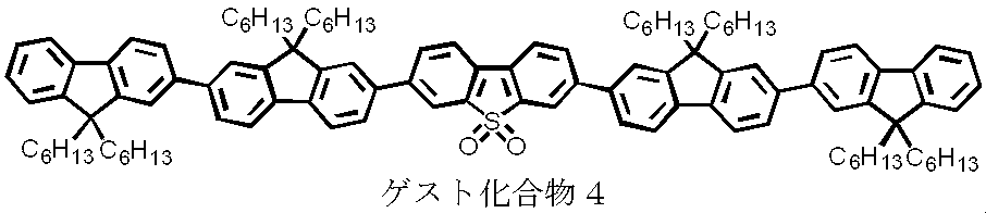
Cz-TEGを79.9質量部、ゲスト化合物として下記式で示されるゲスト化合物5(アメリカンダイソース社製)20.0質量部、TBAPF60.1質量部からなる液体発光材料を用いた以外は実施例1と同様にEL素子を作製し、同様の評価を行った。結果を図17および図18に示す。このデバイスの液体発光層の膜厚を誘電率測定の結果から算出したところ390nmであった。
図17および図18に示されるように、発光は3.6Vから観測され、20.0V印加時に1.35mA/cm2の電流密度、7.0cd/m2の最大輝度、0.23%のEL外部量子効率が得られ、514nmの発光ピークを有する緑色の発光が得られた。

[実施例9]
界面活性剤、純水、イソプロパノールの順で超音波洗浄し、UV/オゾン処理(フィルゲン社製、UV253S)を12分間ほどこしたITOガラス基板を2枚用意した。
一方のITO12付きガラス基板11にPEDOT:PSS(バイエル社製、PI4083)を3000rpmの回転数で30秒間スピンコートして成膜した後、200℃,10分間、大気中で加熱してホール注入層30がITO12上に成膜された陽極側基板10を得た。
次に、もう一方のITO14付きガラス基板13のITO14側に、TiO2をスパッタ法により10nmの膜厚で成膜し、ホールブロック層40が形成された、陰極側基板20を得た。このホールブロック層40の上に、実施例1と同様の液体発光材料を少量滴下し、PEDOT:PSSが成膜された陽極側基板10と挟みこみ、クリップ(図示省略)で固定することで、図1に示されるような、ガラス基板/ITO(陽極)/PEDOT:PSS40nm/液体発光層/TiO2(ホールブロック層)10nm/ITO(陰極)/ガラス基板からなるEL素子1を作製した。素子面積は2mm×2mmである。このデバイスの液体発光層の膜厚を誘電率測定の結果から算出したところ1100nmであった。実施例1と同様に、電流密度、輝度、電圧、ELの外部量子効率、発光スペクトルを評価した。結果を図19および図20に示す。
図19および図20に示されるように、発光は15.0Vから観測され、100V印加時に3.72mA/cm2の電流密度、76.8cd/m2の最大輝度、0.37%の最大のEL外部量子効率が得られ、実施例1と同様に531nmの発光ピークを有する緑色の電界発光が得られた。
EHCz98.9質量部、ゲスト化合物としてルブレン1.0質量部およびTBAPF60.1質量部からなる液体発光材料を用いた以外は実施例9と同様にEL素子を作製し、同様の評価を行った。結果を図21および図22に示す。このデバイスの液体発光層の膜厚を誘電率測定の結果から算出したところ1210nmであった。
図21および図22に示されるように、発光は15.6Vから観測され、47.2V印加時に0.64mA/cm2の電流密度、5.0cd/m2の最大輝度、0.16%の最大のEL外部量子効率が得られ、実施例2と同様に558nmをピークとするオレンジ色の電界発光が得られた。
EHCz99.9質量部およびTBAPF60.1質量部からなる液体発光材料を用いた以外は、実施例9と同様にEL素子を作製し、同様の評価を行った。結果を図23および図24に示す。このデバイスの液体発光層の膜厚を誘電率測定の結果から算出したところ620nmであった。
図23および図24に示されるように、発光は9.6Vから観測され、66.6V印加時に8.5mA/cm2の電流密度、5.7cd/m2の最大輝度、0.10%の最大のEL外部量子効率が得られ、実施例3と同様に474nmを発光ピークとする青色の電界発光が得られた。
[実施例12]
EHCz99.9質量部、イオン性材料として、イオン性液体である1-ブチル-1-メチルピロリジニウムビス(トリフルオロメタンスルホニル)イミド(以下、BMPyTFSI)を0.1質量部からなる液体発光材料を用いた以外は実施例9と同様にEL素子を作製し、同様の評価を行った。結果を図25および図26に示す。このデバイスの液体発光層の膜厚を誘電率測定の結果から算出したところ960nmであった。
図25および図26に示されるように、発光は27.6Vから観測され、96.8V印加時に6.67mA/cm2の電流密度、0.23cd/m2の最大輝度、0.013%の最大のEL外部量子効率が得られ、453nmをピークとする青色の電界発光が得られた。
EHCz98.9質量部、ルブレン1.0質量部、BMPyTFSI0.1質量部かなる液体発光材料を用いた以外は、実施例9と同様にEL素子を作製し、同様の評価を行った。このデバイスの液体発光層の膜厚を誘電率測定の結果から算出したところ960nmであった。
図27および図28に示されるように、発光は7.6Vから観測され、45.2V印加時に1.56mA/cm2の電流密度、32.5cd/m2の最大輝度、0.44%の最大のEL外部量子効率が得られ、557nmをピークとするオレンジ色の電界発光が得られた。
[実施例14]
EHCz99.0質量部、BMPyTFSI1.0質量部からなる液体発光材料を用いた以外は、実施例12と同様にEL素子を作製し、同様の評価を行った。このデバイスの液体発光層の膜厚を誘電率測定の結果から算出したところ1030nmであった。
また、発光は19.0Vから観測され、67.6V印加時に3.50mA/cm2の電流密度、1.7cd/m2の最大輝度、0.20%の最大のEL外部量子効率が得られ、451nmをピークとする青色の電界発光が得られた。
EHCzを90.0質量部、BMPyTFSI10.0質量部からなる液体発光材料を用いた以外は、実施例12と同様にEL素子を作製し、同様の評価を行った。このデバイスの液体発光層の膜厚を誘電率測定の結果から算出したところ1050nmであった。
また、発光は11.2Vから観測され、44.4V印加時に3.54mA/cm2の電流密度、0.20cd/m2の最大輝度、0.035%の最大のEL外部量子効率が得られ、443nmをピークとする青色の電界発光が得られた。
[実施例16]
実施例14の液体発光材料を用い、実施例14と同様にEL素子を作製し、同様の評価を行った。このデバイスの液体発光層の膜厚を誘電率測定の結果から算出したところ880nmであった。
イオン性液体として、1-n-プロピル-1-メチルピロリジニウムビス(トリフルオロメタンスルホニル)イミドを用いた以外は、実施例16と同様にEL素子を作製し、同様の評価を行った。このデバイスの液体発光層の膜厚を誘電率測定の結果から算出したところ840nmであった。
イオン性液体として、トリブチルメチルホスホニウムビス(トリフルオロメタンスルホニル)イミドを用いた以外は、実施例16と同様にEL素子を作製し、同様の評価を行った。このデバイスの液体発光層の膜厚を誘電率測定の結果から算出したところ750nmであった。
[実施例19]
実施例9において、TiO2の膜厚を0nmから20nmまで変化させてEL素子を作製し、実施例9と同様に評価した。
実施例10において、TiO2の膜厚を0nmから20nmまで変化させてEL素子を作製し、実施例10と同様に評価した。
また、実施例19および実施例20で作製したEL素子における、ITO陰極上のTiO2層の原子間力顕微鏡(AFM)にて観察した。得られたAFM像を図32に示す。
図32の(i)と(ii)に示されるように、ITO陰極自体の膜の高低差は2nm程度なのに対して、10nm以下の膜厚を有するTiO2層の場合は、そのTiO2層の高低差が8nm程度であることから、TiO2層がITO陰極上に完全に被腹されておらず、ドット状の膜質になっていることがわかる。それゆえ、TiO2層が8nm以下である場合、ホールのブロック効果は不十分である。
一方で、図32(iii)に示されるように、TiO2膜の高低差は10nm以上の膜厚になっても増加せず、8nm程度とほぼ一定の値を保つ。このことから10nm以上の膜厚では少なくとも、ITO陰極上はTiO2層で完全に被腹されていることがわかる。それゆえ、TiO2層の膜厚が10nm以上の場合は、良好なホールブロック機能が達成されるため、キャリアの再結合確率が改善し、電界発光の外部量子収率が向上していることがわかる。
[実施例21]
EHPy99.9質量部およびTBAPF60.1質量部からなる液体発光材料を、10μmのギャップを有するITOセル(EHC社製)の側面に図33(i)に示すように滴下した。10μmのギャップを有するITOセル間を上記液体発光材料が毛細管現象によって移動する様子を、UVライトにより液体発光材料を発光させながら確認したところ、液体発光材料は図33(ii)~(v)のように上側から下側に約0.2mm/分の速度で移動した。
滴下後5分後、液体発光材料は図33(ii)の状態になり、この際、2枚のITO電極間に170Vの電圧を印加したところ、図33(vi)のように発光は観測されなかった。
滴下後10分後、液体発光材料は図33(iii)の状態になり、この際、2枚のITO電極間に170Vの電圧を印加したところ、図33(vii)のようにITO電極が交差する箇所からのみEHPy由来の青緑色の発光が観測された。
滴下後15分後、液体発光材料は図33(iv)の状態になり、この際、2枚のITO電極間に170Vの電圧を印加したところ、図33(viii)のようにITO電極が交差する箇所全体からEHPy由来の青緑色の発光が観測された。
滴下後30分後、液体発光材料は図33(v)の状態になり、この際、2枚のITO電極間に170Vの電圧を印加したところ、図33(ix)のようにITO電極が交差する箇所全体からEHPy由来の青緑色の発光が観測された。
以上のように、液体発光材料が常に電極間を移動しながら、電界発光が観測されることがわかる。
EHCz83.1質量部、ゲスト化合物2 16.6質量部およびTBAPF60.3質量部からなる液体発光材料を、実施例21と同様の10μmのギャップを有するITOセル(EHC社製)に注入した。
2枚のITO電極間に170Vの電圧を印加したところ、図38(i)の状態になりゲスト化合物2由来の発光が観測された。図38(iv)はその時のPL発光を示した様子である。電圧印加してから5分後、ゲスト化合物2の発光が消失するまで液体発光材料を劣化させた様子を図38(ii)に示している。図38(v)のPL発光においてもITOと接触した部分においては、劣化に由来する発光強度の減少が確認できる。液体発光材料の劣化後、毛細管現象を利用して、新しい液体発光材料を注入させ、170Vの電圧を印加した様子を図38(iii)に示す。これは、劣化した発光材料を新たな液体発光材料で置換することで素子の発光が復元することがわかる。また、図38(vi)のPL発光においては、その劣化した発光材料が流動し、新しい発光材料に置き換わる様子を確認できる。
以上のように、液体発光材料が劣化した後でも新しい液体発光材料を注入することで素子を復元することができる。
[実施例23]
EHPy99.75質量部およびトリブチル(2-メトキシエチル)ホスホニウムビス(トリフルオロメタンスルホニル)イミド0.25質量部からなる液体発光材料を用いた以外は、実施例1と同様にEL素子を作製した。このデバイスの液体発光層の膜厚を誘電率測定の結果から算出したところ1.20±0.06μmであった。作製したEL素子の直流および交流電圧印加時の輝度-電圧特性を測定した。結果を図39に示す。
図39に示されるように、発光は、直流電圧印加時は2.5Vから観測され、10.5V印加時に37.4cd/m2の最大輝度が得られたのに対し、1Hzの交流電圧印加時は2.2Vから発光が観測され、12.0V印加時に115cd/m2の最大輝度が得られた。また、10Hzの交流電圧印加時は10.0Vから発光が観測され、38.0V印加時に92.3cd/m2の最大輝度が得られた。さらに、100Hzの交流電圧印加時は15.0Vから発光が観測され、42.0V印加時に22.8cd/m2の最大輝度が得られた。
以上のように、直流電圧および交流電圧いずれの電圧印加時においても発光が観測されており、交流電圧印加時においても、電界発光が観測されることがわかる。
10 陽極
20 陰極
30 正孔注入層
40 ホールブロック層
50 液体発光層
Claims (10)
- 陽極と、陰極と、これら各極間に介在する、常温で液体の発光層とを備え、前記発光層が、イオン性材料を含むことを特徴とする有機電界発光素子。
- 前記発光層が、キャリア輸送能および発光能を有する材料と、イオン性材料とから構成される請求項1記載の有機電界発光素子。
- 前記発光層が、キャリア輸送材料と、発光材料と、イオン性材料とから構成される請求項1記載の有機電界発光素子。
- 前記イオン性材料が、液状の有機塩、液状の無機塩、液状のキャリア輸送材料または液状の発光材料に分散可能な有機塩、および液状のキャリア輸送材料または液状の発光材料に分散可能な無機塩から選ばれる1種または2種以上である請求項3記載の有機電界発光素子。
- 前記イオン性材料が、式[1]で示される化合物を含む請求項1~4のいずれか1項記載の有機電界発光素子。
(An+)i(Bm-)j [1]
〔式中、An+は、n(nは1~10の整数を表す)価のカチオン成分であって、金属イオン、または窒素原子、リン原子、硫黄原子もしくは酸素原子を含むオニウムイオンを表し、Bm-は、m(mは1~10の整数を表す)価のアニオン成分であって、ハロゲン化物イオン、オキソ酸アニオン、ホウ素原子を含むアニオン、リン原子を含むアニオン、イミド系アニオンを表す。iおよびjは、それぞれ1~100の整数、かつ、式[1]で表されるイオン性材料が電気的中性となる整数である。〕 - 前記イオン性材料が、発光層中に、0.01~50質量%含まれる請求項1~5のいずれか1項記載の有機電界発光素子。
- 前記発光層を含む少なくとも3層の機能層を備える機能分離型薄膜構造を有する請求項1~6のいずれか1項記載の有機電界発光素子。
- 前記機能層として、前記陰極および発光層の間に介在するホールブロック層を有する請求項1~7のいずれか1項記載の有機電界発光素子。
- 前記ホールブロック層が、金属酸化物、金属窒化物、金属硫化物、金属酸化窒化物、高分子化合物を含む請求項8記載の有機電界発光素子。
- 前記ホールブロック層が、Ti,Zr,Ba,Ca,Sr,Yb,Al,Ga,In,Li,Na,Cd,Mg,Si,TaおよびSbから選ばれる金属元素を少なくとも1種含む、酸化物、窒化物、硫化物および酸化窒化物から選ばれる1種または2種以上を含む請求項9記載の有機電界発光素子。
Priority Applications (2)
| Application Number | Priority Date | Filing Date | Title |
|---|---|---|---|
| JP2012526546A JP5875119B2 (ja) | 2010-07-30 | 2011-07-28 | 有機電界発光素子 |
| KR1020137005129A KR101906284B1 (ko) | 2010-07-30 | 2011-07-28 | 유기전계발광소자 |
Applications Claiming Priority (6)
| Application Number | Priority Date | Filing Date | Title |
|---|---|---|---|
| JP2010172095 | 2010-07-30 | ||
| JP2010-172095 | 2010-07-30 | ||
| JP2010-238178 | 2010-10-25 | ||
| JP2010238178 | 2010-10-25 | ||
| JP2011-007614 | 2011-01-18 | ||
| JP2011007614 | 2011-01-18 |
Publications (1)
| Publication Number | Publication Date |
|---|---|
| WO2012014976A1 true WO2012014976A1 (ja) | 2012-02-02 |
Family
ID=45530176
Family Applications (1)
| Application Number | Title | Priority Date | Filing Date |
|---|---|---|---|
| PCT/JP2011/067258 Ceased WO2012014976A1 (ja) | 2010-07-30 | 2011-07-28 | 有機電界発光素子 |
Country Status (4)
| Country | Link |
|---|---|
| JP (1) | JP5875119B2 (ja) |
| KR (1) | KR101906284B1 (ja) |
| TW (1) | TWI577065B (ja) |
| WO (1) | WO2012014976A1 (ja) |
Cited By (5)
| Publication number | Priority date | Publication date | Assignee | Title |
|---|---|---|---|---|
| WO2012099237A1 (ja) * | 2011-01-20 | 2012-07-26 | 国立大学法人九州大学 | 有機電界発光素子 |
| WO2012099236A1 (ja) * | 2011-01-20 | 2012-07-26 | 国立大学法人九州大学 | 有機電界発光素子 |
| WO2012099240A1 (ja) * | 2011-01-20 | 2012-07-26 | 国立大学法人九州大学 | 有機電界白色発光素子 |
| JP2015524161A (ja) * | 2012-05-10 | 2015-08-20 | メルク パテント ゲゼルシャフト ミット ベシュレンクテル ハフツングMerck Patent Gesellschaft mit beschraenkter Haftung | 電子輸送層において使用するためのイオン性有機化合物を含む配合物 |
| RU2714256C2 (ru) * | 2011-06-10 | 2020-02-13 | Конинклейке Недерландсе Академи Ван Ветенсаппен (Кнав) | Культуральная среда стволовых клеток |
Families Citing this family (2)
| Publication number | Priority date | Publication date | Assignee | Title |
|---|---|---|---|---|
| CN104716268B (zh) | 2013-12-17 | 2017-09-29 | 北京维信诺科技有限公司 | 一种有机电致发光器件及其制备方法 |
| CN109804027B (zh) | 2016-11-25 | 2022-03-01 | 株式会社Lg化学 | 离子化合物、包含其的涂覆组合物和有机发光二极管 |
Citations (4)
| Publication number | Priority date | Publication date | Assignee | Title |
|---|---|---|---|---|
| JP2006261576A (ja) * | 2005-03-18 | 2006-09-28 | Fujikura Ltd | 有機el素子及びその製造方法 |
| JP2007204749A (ja) * | 2006-01-27 | 2007-08-16 | Samsung Sdi Co Ltd | 高効率の有機電界発光素子 |
| JP2008303365A (ja) * | 2007-06-11 | 2008-12-18 | Toppan Printing Co Ltd | 蛍光材料、発光インク組成物および有機el素子 |
| WO2011010656A1 (ja) * | 2009-07-21 | 2011-01-27 | 国立大学法人九州大学 | 有機電界発光素子 |
-
2011
- 2011-07-28 KR KR1020137005129A patent/KR101906284B1/ko active Active
- 2011-07-28 JP JP2012526546A patent/JP5875119B2/ja active Active
- 2011-07-28 WO PCT/JP2011/067258 patent/WO2012014976A1/ja not_active Ceased
- 2011-07-29 TW TW100127038A patent/TWI577065B/zh active
Patent Citations (4)
| Publication number | Priority date | Publication date | Assignee | Title |
|---|---|---|---|---|
| JP2006261576A (ja) * | 2005-03-18 | 2006-09-28 | Fujikura Ltd | 有機el素子及びその製造方法 |
| JP2007204749A (ja) * | 2006-01-27 | 2007-08-16 | Samsung Sdi Co Ltd | 高効率の有機電界発光素子 |
| JP2008303365A (ja) * | 2007-06-11 | 2008-12-18 | Toppan Printing Co Ltd | 蛍光材料、発光インク組成物および有機el素子 |
| WO2011010656A1 (ja) * | 2009-07-21 | 2011-01-27 | 国立大学法人九州大学 | 有機電界発光素子 |
Non-Patent Citations (2)
| Title |
|---|
| DENGHUI XU ET AL.: "Organic light- emitting diode with liquid emitting layer", APPLIED PHYSICS LETTER, vol. 95, 6 August 2009 (2009-08-06), pages 053304-1 - 053304-3 * |
| SHUZO HIRATA ET AL.: "Improvement of Electroluminescence Performance of Organic Light-Emitting Diodes with a Liquid-Emitting Layer by Introduction of Electrolyte and a Hole-Blocking Layer", ADVANCED MATERIALS, vol. 23, 22 December 2010 (2010-12-22), pages 889 - 893 * |
Cited By (6)
| Publication number | Priority date | Publication date | Assignee | Title |
|---|---|---|---|---|
| WO2012099237A1 (ja) * | 2011-01-20 | 2012-07-26 | 国立大学法人九州大学 | 有機電界発光素子 |
| WO2012099236A1 (ja) * | 2011-01-20 | 2012-07-26 | 国立大学法人九州大学 | 有機電界発光素子 |
| WO2012099240A1 (ja) * | 2011-01-20 | 2012-07-26 | 国立大学法人九州大学 | 有機電界白色発光素子 |
| JP5888748B2 (ja) * | 2011-01-20 | 2016-03-22 | 国立大学法人九州大学 | 有機電界白色発光素子 |
| RU2714256C2 (ru) * | 2011-06-10 | 2020-02-13 | Конинклейке Недерландсе Академи Ван Ветенсаппен (Кнав) | Культуральная среда стволовых клеток |
| JP2015524161A (ja) * | 2012-05-10 | 2015-08-20 | メルク パテント ゲゼルシャフト ミット ベシュレンクテル ハフツングMerck Patent Gesellschaft mit beschraenkter Haftung | 電子輸送層において使用するためのイオン性有機化合物を含む配合物 |
Also Published As
| Publication number | Publication date |
|---|---|
| JPWO2012014976A1 (ja) | 2013-09-12 |
| JP5875119B2 (ja) | 2016-03-02 |
| TW201218477A (en) | 2012-05-01 |
| KR20140023246A (ko) | 2014-02-26 |
| KR101906284B1 (ko) | 2018-10-11 |
| TWI577065B (zh) | 2017-04-01 |
Similar Documents
| Publication | Publication Date | Title |
|---|---|---|
| KR101853014B1 (ko) | 유기 발광 다이오드에서 양극성 호스트 | |
| JP6668755B2 (ja) | イリジウム錯体化合物、該化合物の製造方法、該化合物を含む組成物、有機電界発光素子、表示装置及び照明装置 | |
| JP5355962B2 (ja) | 発光素子、発光装置および電子機器 | |
| TWI395358B (zh) | 用於有機電光元件之具有茀衍生化合物的材料以及包含此之有機電光元件 | |
| CN102473853B (zh) | 有机电致发光元件 | |
| JP5875119B2 (ja) | 有機電界発光素子 | |
| JP5773585B2 (ja) | 発光性トリアリール | |
| US8941099B2 (en) | Organic light emitting device and materials for use in same | |
| JP4690244B2 (ja) | テトラ−フェニルシラン骨格を有するフルオレン化合物、それを用いた発光層ホスト材料、ホールブロック材料および有機el素子 | |
| KR101567784B1 (ko) | 용액공정이 가능한 신규한 이리듐(iii) 착화합물 및 이를 포함하는 유기전계발광소자 | |
| JP5888748B2 (ja) | 有機電界白色発光素子 | |
| WO2012099236A1 (ja) | 有機電界発光素子 | |
| WO2013089217A1 (ja) | 有機電界発光素子 | |
| JP2022512115A (ja) | 組成物および有機発光デバイス | |
| KR20190064010A (ko) | 유기 화합물과 이를 포함하는 유기발광다이오드 및 유기발광 표시장치 | |
| WO2012099237A1 (ja) | 有機電界発光素子 | |
| JP2014049469A (ja) | 有機電界発光素子 | |
| JP2019123689A (ja) | 化合物、組成物、液状組成物、有機エレクトロルミネッセンス素子用材料、及び有機エレクトロルミネッセンス素子 | |
| JP2020132544A (ja) | カルバゾール誘導体、それよりなるホスト材料及びそれを用いた有機el素子 | |
| KR20180127904A (ko) | 신규 열활성 지연형광 재료 및 이를 포함하는 유기발광 다이오드 소자 |
Legal Events
| Date | Code | Title | Description |
|---|---|---|---|
| 121 | Ep: the epo has been informed by wipo that ep was designated in this application |
Ref document number: 11812565 Country of ref document: EP Kind code of ref document: A1 |
|
| WWE | Wipo information: entry into national phase |
Ref document number: 2012526546 Country of ref document: JP |
|
| NENP | Non-entry into the national phase |
Ref country code: DE |
|
| ENP | Entry into the national phase |
Ref document number: 20137005129 Country of ref document: KR Kind code of ref document: A |
|
| 122 | Ep: pct application non-entry in european phase |
Ref document number: 11812565 Country of ref document: EP Kind code of ref document: A1 |