WO2012014376A1 - Micro-ordinateur destiné à détecter un champ magnétique, et procédé de détection d'un champ magnétique - Google Patents
Micro-ordinateur destiné à détecter un champ magnétique, et procédé de détection d'un champ magnétique Download PDFInfo
- Publication number
- WO2012014376A1 WO2012014376A1 PCT/JP2011/003762 JP2011003762W WO2012014376A1 WO 2012014376 A1 WO2012014376 A1 WO 2012014376A1 JP 2011003762 W JP2011003762 W JP 2011003762W WO 2012014376 A1 WO2012014376 A1 WO 2012014376A1
- Authority
- WO
- WIPO (PCT)
- Prior art keywords
- magnetic field
- voltage
- field detection
- output
- voltage control
- Prior art date
Links
Images


Classifications
-
- G—PHYSICS
- G01—MEASURING; TESTING
- G01R—MEASURING ELECTRIC VARIABLES; MEASURING MAGNETIC VARIABLES
- G01R33/00—Arrangements or instruments for measuring magnetic variables
- G01R33/02—Measuring direction or magnitude of magnetic fields or magnetic flux
-
- G—PHYSICS
- G01—MEASURING; TESTING
- G01R—MEASURING ELECTRIC VARIABLES; MEASURING MAGNETIC VARIABLES
- G01R33/00—Arrangements or instruments for measuring magnetic variables
- G01R33/0023—Electronic aspects, e.g. circuits for stimulation, evaluation, control; Treating the measured signals; calibration
-
- G—PHYSICS
- G01—MEASURING; TESTING
- G01R—MEASURING ELECTRIC VARIABLES; MEASURING MAGNETIC VARIABLES
- G01R33/00—Arrangements or instruments for measuring magnetic variables
- G01R33/02—Measuring direction or magnitude of magnetic fields or magnetic flux
- G01R33/06—Measuring direction or magnitude of magnetic fields or magnetic flux using galvano-magnetic devices
- G01R33/07—Hall effect devices
- G01R33/072—Constructional adaptation of the sensor to specific applications
-
- G—PHYSICS
- G06—COMPUTING; CALCULATING OR COUNTING
- G06F—ELECTRIC DIGITAL DATA PROCESSING
- G06F17/00—Digital computing or data processing equipment or methods, specially adapted for specific functions
-
- H—ELECTRICITY
- H10—SEMICONDUCTOR DEVICES; ELECTRIC SOLID-STATE DEVICES NOT OTHERWISE PROVIDED FOR
- H10B—ELECTRONIC MEMORY DEVICES
- H10B61/00—Magnetic memory devices, e.g. magnetoresistive RAM [MRAM] devices
-
- H—ELECTRICITY
- H10—SEMICONDUCTOR DEVICES; ELECTRIC SOLID-STATE DEVICES NOT OTHERWISE PROVIDED FOR
- H10N—ELECTRIC SOLID-STATE DEVICES NOT OTHERWISE PROVIDED FOR
- H10N59/00—Integrated devices, or assemblies of multiple devices, comprising at least one galvanomagnetic or Hall-effect element covered by groups H10N50/00 - H10N52/00
Definitions
- the present invention relates to a magnetic field detection microcomputer having a magnetic field detection function and a magnetic field detection method.
- the degree of integration of system LSIs has been improving year by year as the functions of sets and process miniaturization are reduced.
- the conventional one-chip device system composed of a plurality of chips is being realized.
- the sensor system analog block is particularly difficult to make into one chip. Since the sensor system analog block handles minute analog signals, the semiconductor process for increasing the sensitivity of the sensor and the process for improving the low cost miniaturization are not necessarily the same process.
- FIG. 21 is a diagram showing a sensor IC and a microcomputer in the prior art.
- the sensor ICX and the microcomputer Y are composed of two chips, and an output terminal X3 for outputting a signal from the sensor ICX and an input terminal X4 for inputting a signal to the sensor ICX are signal lines.
- an output terminal X3 for outputting a signal from the sensor ICX and an input terminal X4 for inputting a signal to the sensor ICX are signal lines.
- it is connected to the microcomputer Y via (see, for example, Patent Document 1).
- FIG. 22 is a diagram showing a magnetic field detection circuit in the prior art. As shown in FIG. 22, the following processing is performed to improve the temperature characteristics of the sensor IC.
- the output OUTA of the Hall element HAL1 amplified by the amplifier circuit AMP1 is input to the comparison circuit CMP1.
- the reference voltage circuit BL1 includes only a voltage dividing circuit that generates the reference voltages VTH1 and VTH2, and compensates for temperature. Of the reference voltages VTH1 and VTH2 generated by the reference voltage circuit BL1, one reference voltage having a temperature coefficient substantially equal to the temperature coefficient of the output OUTA is selected by the switch circuit SW1 and input to the comparison circuit CMP1 as the reference voltage OUTB.
- the comparison circuit CMP1 compares the output OUTA and the reference voltage OUTB, and cancels the temperature characteristic in the correlation of the reference potential generation circuit that compares the output with the sensor so as to detect the magnetic field based on the value of the output OUT.
- a method for improving the performance of a single sensor IC with such a configuration is disclosed (for example, see Patent Document 2).
- the technique of Patent Document 2 is also referred to as Conventional Technique B.
- JP 2008-032424 A (page 29, FIG. 19) JP 2009-047478 A (page 10, FIG. 4, FIG. 3)
- the configuration of the prior art B requires a voltage variable circuit (reference voltage circuit BL1) that generates two types of reference voltages by combining resistors having two or more types of temperature characteristic coefficients for canceling the temperature characteristics. . Therefore, the configuration of the voltage variable circuit of the conventional technique B is complicated.
- Patent Document 1 describes a combination example of a sensor IC and a microcomputer, but does not describe a technique for easily determining the presence or absence of magnetic field strength.
- the present invention solves the above-described conventional problems, and provides a magnetic field detection microcomputer and a magnetic field detection method capable of easily determining the presence or absence of a magnetic field strength without requiring a complicated voltage variable circuit. Objective.
- a magnetic field detection microcomputer includes a magnetic field detection element for detecting a magnetic field, a differential amplifier that amplifies the output voltage of the magnetic field detection element, and a voltage control signal.
- a voltage variable circuit that generates a variable reference voltage; a comparator that compares an output of the differential amplifier with a reference voltage generated by the voltage variable circuit; and a level of the reference voltage generated by the voltage variable circuit.
- a voltage control register that holds a voltage control value for controlling and outputs the voltage control signal having the voltage control value to the voltage variable circuit; a magnetic field strength that is a magnetic field strength applied to the magnetic field detection element; and A storage unit that stores in advance a first table in association with the voltage control value immediately before or immediately after the output of the comparator is inverted when the voltage control value is increased or decreased; Set the voltage control value corresponding to the magnetic field of the detection object to the voltage control register comprises comparison result and from the first table of the comparator, the CPU determines the presence or absence of the magnetic field intensity corresponding to the voltage control value.
- the voltage control value and the magnetic field strength are stored in advance in the storage unit, and the voltage control value can be handled by a simple process of setting the voltage control value corresponding to the magnetic field to be detected in the voltage control register.
- the presence or absence of the magnetic field strength to be determined can be determined. That is, the presence or absence of the magnetic field intensity corresponding to the voltage control value can be easily determined.
- the conventional voltage variable circuit is configured to generate two types of reference voltages.
- the voltage variable circuit of the magnetic field detection microcomputer in one embodiment of the present invention is configured to generate one reference voltage. Therefore, the configuration of the voltage variable circuit of the magnetic field detection microcomputer in one embodiment of the present invention can be simplified. Therefore, it is possible to easily determine the presence or absence of magnetic field strength without requiring a voltage variable circuit having a complicated configuration.
- the differential amplifier is variable in gain according to a gain control signal
- the magnetic field detection microcomputer further holds a gain control value for setting the gain of the differential amplifier, and the gain control value
- a gain control register that outputs a gain control signal having a value to the differential amplifier may be provided, and the first table may store the magnetic field strength and the voltage control value in advance for each gain control value.
- the sensitivity for detecting the magnetic field can be controlled by setting the gain.
- the CPU sequentially increases or decreases the voltage control value held in the voltage control register, and when the output of the comparator is inverted, the magnetic field strength corresponding to the voltage control value is changed to the first voltage control value. You may make it read as a magnetic field intensity detected from the table.
- This configuration can accurately detect a wide range of magnetic field strengths.
- the voltage variable circuit may be a D / A converter.
- the magnetic field detection microcomputer further stores in advance a magnetic field intensity of the south pole applied to the magnetic field detection element and a voltage control value indicating a condition for inverting the output of the comparator
- the first table includes: You may make it memorize
- the direction (polarity) of the magnetic field can be detected.
- the CPU may alternately perform magnetic field detection using the first table and magnetic field detection using the second table a predetermined number of times.
- the presence / absence of a magnetic field in a different direction can be efficiently detected by time division alternately every predetermined number of times.
- the magnetic field detection microcomputer further selects a booster circuit that boosts the power supply voltage, one of the boosted power supply voltage and the power supply voltage that is not boosted, and supplies the selected power supply voltage to the magnetic field detection element.
- a voltage switching circuit wherein the first table stores in advance the magnetic field strength and the voltage control value corresponding to each of the boosted power supply voltage and the unboosted power supply voltage, and the CPU stores the voltage
- the magnetic field strength may be detected using a voltage control value corresponding to the power supply voltage selected by the switching circuit.
- the sensitivity of the magnetic field detecting element can be switched by selecting a boosted power supply voltage and an unboosted power supply voltage.
- the magnetic field detection element is a Hall element
- the magnetic field detection element, the differential amplifier, the voltage variable circuit, the comparator, the voltage control register, the storage unit, and the CPU are on the same semiconductor substrate. It may be formed.
- the magnetic field detection element, the amplifier, the voltage variable circuit, the comparator, the voltage control register, the storage unit, and the CPU can be realized on the same semiconductor substrate in the same process, the area and cost can be reduced. can do.
- the Hall element may be formed in at least one of the four corners of the semiconductor substrate.
- the Hall element is disposed at least at one of the four corners that have conventionally been a free area of the semiconductor substrate, the circuit area can be reduced. In addition, the area where circuits other than the Hall element can be formed can be increased.
- the magnetic field detection microcomputer further includes three magnetic field detection elements having the same configuration as the magnetic field detection element, and three sets having the same configuration as the set including the differential amplifier, the voltage variable circuit, and the comparator.
- the four magnetic field detection elements may be arranged at four corners of the semiconductor substrate, and the CPU may detect a magnetic field using each of the four sets.
- the magnetic field detection elements are arranged at the four corners on the diagonal line of the semiconductor substrate, the direction of the magnetic field can be sensitively detected.
- a magnetic field detection method is a magnetic field detection method in a magnetic field detection microcomputer, wherein the magnetic field detection microcomputer is configured to detect a magnetic field and a difference in which an output voltage of the magnetic field detection element is amplified.
- a dynamic amplifier a voltage variable circuit that generates a reference voltage that is variable according to a voltage control signal, a comparator that compares an output of the differential amplifier with a reference voltage generated by the voltage variable circuit, and the voltage A voltage control register that holds a voltage control value for controlling the level of the reference voltage generated by the variable circuit and outputs the voltage control signal having the voltage control value to the voltage variable circuit, and the magnetic field detection element
- the magnetic field strength which is the strength of the magnetic field, is associated with the voltage control value immediately before or immediately after the output of the comparator is inverted when the voltage control value is increased or decreased.
- the magnetic field detection method sets a voltage control value corresponding to the magnetic field to be detected in the voltage control register, and determines whether or not the output of the comparator is inverted. If it is determined that the output of the comparator is inverted, the magnetic field intensity corresponding to the voltage control value is read from the first table.
- the magnetic field detection microcomputer of the present invention it is possible to easily determine the presence or absence of magnetic field strength without requiring a complicated voltage variable circuit.
- FIG. 1 is a block diagram of a magnetic field detection microcomputer according to the first embodiment of the present invention.
- FIG. 2A is a magnetic field detection determination table.
- FIG. 2B is a magnetic field detection determination table for detecting a magnetic field having a reverse polarity.
- FIG. 2C is a magnetic field detection determination table including a gain control value.
- FIG. 3 is an operation timing chart of magnetic field detection.
- FIG. 4A is a diagram showing an overall processing flow of the magnetic field detection setting algorithm.
- FIG. 4B is a diagram illustrating a processing flow of the sample variation correction algorithm in the magnetic field detection setting algorithm.
- FIG. 4C is a diagram illustrating a processing flow of the magnetic field X determination processing.
- FIG. 4A is a diagram showing an overall processing flow of the magnetic field detection setting algorithm.
- FIG. 4B is a diagram illustrating a processing flow of the sample variation correction algorithm in the magnetic field detection setting algorithm.
- FIG. 4C is a diagram illustrating a processing flow of
- FIG. 4D is a diagram illustrating a processing flow of the magnetic field Y determination processing.
- FIG. 4E is a diagram illustrating a processing flow of magnetic field Z determination processing.
- FIG. 5 is an operation timing chart when the magnetic field detection setting algorithm is executed.
- FIG. 6 is a block diagram of the magnetic field detection microcomputer according to the second embodiment of the present invention.
- FIG. 7 is a diagram illustrating the relationship between the microcomputer and the magnet.
- FIG. 8 is a setting algorithm and operation timing chart of positive magnetic field detection when approaching the N pole side according to the third embodiment of the present invention.
- FIG. 9 is a setting algorithm and operation timing chart for detecting the negative magnetic field when approaching the south pole side according to the third embodiment of the present invention.
- FIG. 10 is an N pole / S pole application determination microcomputer execution sequence according to the third embodiment of the present invention.
- FIG. 11 is a diagram illustrating an internal circuit of the voltage variable circuit.
- FIG. 12 is a diagram illustrating an internal circuit of the differential amplifier.
- FIG. 13 is a block diagram of a magnetic field detection microcomputer according to the fourth embodiment of the present invention.
- FIG. 14 is a perspective view of a semiconductor substrate used in the magnetic field detection microcomputer according to the fifth embodiment of the present invention.
- FIG. 15 is a semiconductor layout diagram of the magnetic field detection microcomputer according to the sixth embodiment of the present invention.
- FIG. 16 is a detailed layout diagram of the area of FIG.
- FIG. 17 is a block diagram of a magnetic field detection microcomputer according to the seventh embodiment of the present invention.
- FIG. 11 is a diagram illustrating an internal circuit of the voltage variable circuit.
- FIG. 12 is a diagram illustrating an internal circuit of the differential amplifier.
- FIG. 13 is a block diagram of a magnetic field
- FIG. 18 is an operation timing chart of the magnetic field detection microcomputer according to the seventh embodiment of the present invention.
- FIG. 19 shows a semiconductor layout diagram and a magnetic field application state of the magnetic field detection microcomputer according to the seventh embodiment of the invention.
- FIG. 20 is a block diagram showing a characteristic functional configuration of the magnetic field detection microcomputer.
- FIG. 21 is a diagram showing a sensor IC and a microcomputer in the prior art.
- FIG. 22 is a diagram showing a magnetic field detection circuit in the prior art.
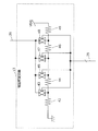
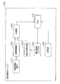
- FIG. 1 is a block diagram of the magnetic field detection microcomputer 19 according to the first embodiment of the present invention, the magnetic field detection determination table of FIG. 2A, the operation timing chart of the magnetic field detection of FIG. The algorithm and the operation timing chart when executing the magnetic field detection setting algorithm of FIG. 5 will be described.
- the magnetic field detection determination table of FIG. 2A is also simply referred to as the table of FIG. 2A.
- the magnetic field detection microcomputer 19 includes a magnetic field detection element 10 having four terminals, a differential amplifier 11 that amplifies the output voltage of the magnetic field detection element 10, and an output and voltage variable of the differential amplifier 11.
- a comparator 12 that compares the reference voltage generated by the circuit 13, a CPU 15, a ROM 16, a RAM 17, and a peripheral logic 18 are provided.
- the magnetic field detection element 10 is an element for detecting a magnetic field.
- the terminal 23 as the first terminal of the magnetic field detection element 10 is connected to the high-potential side VDD via the switch 30.
- the terminal 24 as the second terminal is connected to the low potential side potential VSS via the switch 31, and the terminal 21 as the third terminal and the terminal 22 as the fourth terminal are connected to the input of the differential amplifier 11. Connected.
- the switch 30 and the switch 31 are turned on when the magnetic field is detected and the table unit 16a is set under the control of the CPU 15.
- the component A when expressing a configuration in which the component A is connected to a signal line for transmitting a signal such as a control signal and an output, the component A is expressed as being connected to a signal (control signal, output, etc.) .
- the component A when expressing a configuration in which the component A is connected to a signal line that transmits a control signal, the component A is expressed as being connected to a control signal.
- the component A when expressing a configuration in which the component A is connected to a signal line that transmits an output of a certain circuit, the component A is expressed as being connected to an output.
- the differential amplifier 11 is variable in gain, that is, the amplification degree of the output 25 (output voltage) can be switched according to the control signal 28 as a gain control signal. That is, the differential amplifier 11 is variable in gain according to the gain control signal.
- the control signal 28 is connected to the peripheral logic 18 (register 4A).
- the output 25 of the differential amplifier 11 is connected to the + input of the comparator 12.
- the output 26 of the voltage variable circuit 13 is connected to the negative input of the comparator 12 as a reference voltage. That is, the output 26 of the voltage variable circuit 13 is a reference voltage generated by the voltage variable circuit 13. That is, the output 26 is an analog output.
- the voltage variable circuit 13 is connected to a control signal 29 as a voltage control signal.
- the voltage variable circuit 13 generates a variable reference voltage (voltage of the output 26).
- the control signal 29 as a voltage control signal has a voltage control value for controlling the level of the reference voltage generated by the voltage variable circuit 13. That is, the control signal 29 as a voltage control signal is a signal for changing the level of the reference voltage generated by the voltage variable circuit 13. That is, the voltage variable circuit 13 generates a variable reference voltage (voltage of the output 26) according to the control signal 29 as a voltage control signal.
- the comparator 12 compares the output 25 of the differential amplifier 11 with the reference voltage generated by the voltage variable circuit 13. Then, the comparator 12 outputs the result of the comparison as an output 27.
- the output 27 is a signal indicating the H level (1) or the L level (0).
- the peripheral logic 18 is connected to the control signal 29.
- the output 27 of the comparator 12 is connected to the peripheral logic 18.
- the CPU 15, ROM 16, RAM 17, and peripheral logic 18 are connected to a common BUS 1J.
- the register 4A is a gain control register that holds a gain control value and outputs a gain control signal (control signal 28) having the gain control value to the differential amplifier 11.
- the gain control value is a value for setting the gain of the differential amplifier.
- the register 4B holds a voltage control value for controlling the level of the reference voltage generated by the voltage variable circuit 13, and outputs a voltage control signal (control signal 29) having the voltage control value to the voltage variable circuit 13.
- Control register The voltage variable circuit 13 generates a variable reference voltage (voltage of the output 26) in accordance with a voltage control value included in the voltage control signal (control signal 29). That is, the voltage variable circuit 13 generates a variable reference voltage (voltage of the output 26) according to the control signal 29 as a voltage control signal.
- the ROM 16 includes a table portion 16a.
- the table unit 16a has tables as shown in FIGS. 2A to 2C.
- the magnetic field detection determination table in FIG. 2A is the following first table. That is, the ROM 16 as a storage unit includes a magnetic field strength that is a magnetic field strength applied to the magnetic field detection element 10 and a voltage control value immediately before or after the output of the comparator is inverted when the voltage control value is increased or decreased. Are stored in advance as a first table (magnetic field detection determination table in FIG. 2A).
- the strength of the magnetic field applied to the magnetic field detection element 10 is the strength of the magnetic field applied to the magnetic field detection element 10.
- the magnetic field detection element 10 is a sensor (element) for detecting (detecting) the intensity of the magnetic field applied to the magnetic field detection element 10.
- the X axis, the Y axis, and the Z axis that are orthogonal to each other are defined.
- one direction and the other direction of two directions along the X axis are also referred to as an X direction and a ⁇ X direction, respectively.
- One direction and the other direction of the two directions along the Y axis are also referred to as a Y direction and a ⁇ Y direction, respectively.
- One direction and the other direction of the two directions along the Z axis are also referred to as a Z direction and a ⁇ Z direction, respectively.
- the magnetic field in the X direction is also referred to as a magnetic field X or an X magnetic field.
- a magnetic field in the ⁇ X direction is also referred to as a magnetic field ⁇ X or a ⁇ X magnetic field.
- the magnetic field in the Y direction is also referred to as a magnetic field Y or a Y magnetic field.
- the magnetic field in the ⁇ Y direction is also referred to as a magnetic field ⁇ Y or a ⁇ Y magnetic field.
- the magnetic field in the Z direction is also referred to as a magnetic field Z or a Z magnetic field.
- a magnetic field in the ⁇ Z direction is also referred to as a magnetic field ⁇ Z or a ⁇ Z magnetic field.
- the CPU 15 applies a known magnetic field (for example, any one of the no magnetic field, the magnetic field X, the magnetic field Y, and the magnetic field Z in FIG. 2A) as shown in FIG. 10, the value held in the voltage control register (register 4B) is sequentially increased or decreased. Then, when the output of the comparator 12 is inverted, the CPU 15 writes the value of the register 4B immediately before or after the inversion to the first table as a voltage control value corresponding to the known magnetic field.
- a known magnetic field for example, any one of the no magnetic field, the magnetic field X, the magnetic field Y, and the magnetic field Z in FIG. 2A
- the CPU 15 When detecting the magnetic field (for example, detecting the presence or absence of the magnetic field X), the CPU 15 sets the voltage control value corresponding to the magnetic field to be detected to the voltage control register (register 4B) as shown in FIGS. 2A to 2C. Set to. Then, the CPU 15 determines whether or not the output of the comparator 12 is inverted. When it is determined that the output of the comparator 12 is inverted, the CPU 15 reads the magnetic field strength corresponding to the voltage control value set in the voltage control register (register 4B) from the first table. Thereby, CPU15 determines the presence or absence of the magnetic field intensity corresponding to the said voltage control value.
- the CPU 15 determines the presence / absence of the magnetic field intensity corresponding to the voltage control value from the comparison result of the comparator 12 and the first table.
- the CPU 15 sequentially increases or decreases the voltage control value held in the voltage control register (register 4B), and corresponds to the voltage control value when the output of the comparator is inverted.
- the magnetic field strength may be read as the detected magnetic field strength from the first table.
- control signal 28 for switching the amplification degree of the differential amplifier 11 the control signal 29 for switching the reference voltage of the voltage variable circuit 13, and the output 27 of the comparator 12 are respectively in the peripheral logic 18 block.
- the microcomputer corresponds to a magnetic field detection microcomputer (for example, the magnetic field detection microcomputer 19) described in each embodiment.
- the output 27 (0 or 1) of the comparator 12 is written in the register 4C.
- 0 is a value corresponding to the L level.
- 1 is a value corresponding to the H level.
- L level and H level may be written as L and H, respectively.
- the CPU 15 always refers to the value of the register 4C and determines whether or not the output of the comparator 12 (value of the register 4C) is inverted.
- the inversion of the output of the comparator 12 means that the value of the register 4C changes.
- the change in the value of the register 4C is, for example, a change from 0 (L) to 1 (H).
- the CPU 15 When it is determined that the output 27 of the comparator 12 is inverted, the CPU 15 reads out the magnetic field intensity corresponding to the voltage control value set in the voltage control register (register 4B) from the first table in the ROM 16. . In this case, the CPU 15 determines that there is a magnetic field intensity corresponding to the voltage control value. On the other hand, when it is not determined that the output 27 of the comparator 12 is inverted, the CPU 15 determines that there is no magnetic field intensity corresponding to the voltage control value. Thereby, CPU15 determines the presence or absence of the magnetic field intensity corresponding to the said voltage control value.
- the magnetic field detection element 10 generates a voltage proportional to the magnitude of the magnetic field applied in the vertical direction on the plane of the magnetic field detection element 10 between the terminals 21 and 22.
- the differential amplifier 11 increases the difference voltage between the terminals 21 and 22 to an arbitrary amplification factor and outputs an analog voltage to the output 25.
- the output 25 is an analog output.
- the amplification magnification of the differential amplifier 11 can be set to 2 or 4 by writing an arbitrary digital value in the register 4A by a microcomputer program.
- the comparator 12 compares the output 25 of the differential amplifier 11 with the output 26 of the voltage variable circuit 13. When the output 25 is larger, the output 27 of the comparator 12 indicates H level (1), and when the output 25 is smaller than the output 26, the output 27 of the comparator 12 is L level (0). Indicates.
- FIG. 2A is a magnetic field detection determination table.
- the magnetic field strength X [mT] is the strength of the magnetic field in the X direction.
- the magnetic field strength Y [mT] is the strength of the magnetic field in the Y direction.
- the magnetic field strength Z [mT] is the strength of the magnetic field in the Z direction.
- a magnetic field having a magnetic field strength X [mT] is also referred to as a magnetic field X [mT] or X [mT].
- a magnetic field having a magnetic field strength Y [mT] is also referred to as a magnetic field Y [mT] or Y [mT].
- a magnetic field having a magnetic field strength Z [mT] is also referred to as a magnetic field Z [mT] or Z [mT].
- a magnetic field having a magnetic field strength X [mT] in the ⁇ X direction is also referred to as a magnetic field ⁇ X [mT] or ⁇ X [mT].
- a magnetic field having a magnetic field strength Y [mT] in the ⁇ Y direction is also referred to as a magnetic field ⁇ Y [mT] or ⁇ Y [mT].
- a magnetic field having a magnetic field strength Z [mT] in the ⁇ Z direction is also referred to as a magnetic field ⁇ Z [mT] or ⁇ Z [mT].
- the magnetic field detection determination table in FIG. 2A can have a plurality of magnetic field strengths Y [mT] and Z [mT].
- FIG. 2B is a magnetic field detection determination table for detecting a magnetic field having a polarity opposite to that of FIG. 2A.
- the magnetic field detection determination table of FIG. 2B is also simply referred to as the table of FIG. 2B.
- ⁇ X [mT] is the intensity of the magnetic field in the ⁇ X direction.
- -Y [mT] is the intensity of the magnetic field in the -Y direction.
- ⁇ Z [mT] is the intensity of the magnetic field in the ⁇ Z direction.
- FIG. 2C is a magnetic field detection determination table including a gain control value for setting the amplification factor (gain) of the differential amplifier 11.
- the gain control value is written as G1, for example.
- the magnetic field applied to the magnetic field detection element 10 when an N-pole magnet is brought close to the surface of the magnetic field detection element 10 in the vertical direction is defined as a positive magnetic field.
- the magnetic field applied to the magnetic field detection element 10 when the S-pole magnet is brought close to the surface of the magnetic field detection element 10 is defined as a negative magnetic field.
- At least one magnetic field detection determination table shown in FIGS. 2A to 2C is written in the ROM 16 in advance, and the magnetic field detection operation timing shown in FIG. The operation shown in the chart is performed.
- the processing in FIG. 3 is performed by the CPU 15.
- the CPU 15 sets a digital code X1 in the register 4B in advance for a magnetic field to be detected (for example, a magnetic field X [mT]) (S11).
- a magnetic field X [mT] for example, a magnetic field X [mT]
- the output 27 of the comparator 12 becomes L (S13).
- the output 27 of the comparator 12 indicates H (S14). In this case, 1 is written to the register 4C.
- the CPU 15 performs magnetic field detection based on whether or not the value of the register 4C has changed, that is, whether or not the output 27 of the comparator 12 has been inverted.
- FIG. 4B is a diagram showing a processing flow of the sample variation correction algorithm in the magnetic field detection setting algorithm of FIG. 4A.
- a sample is the magnetic field detection element 10 as a sensor.
- FIG. 4C is a diagram showing a processing flow of magnetic field X determination processing in the magnetic field detection setting algorithm of FIG. 4A.
- FIG. 4D is a diagram showing a processing flow of magnetic field Y determination processing in the magnetic field detection setting algorithm of FIG. 4A.
- FIG. 4E is a diagram showing a processing flow of magnetic field Z determination processing in the magnetic field detection setting algorithm of FIG. 4A.
- an arbitrary digital value can be set in the register 4B by a microcomputer program.
- the output 26 of the voltage variable circuit 13 increases in proportion to the digital value to be set.
- FIG. 11 shows a block internal circuit of the voltage variable circuit 13.
- the voltage variable circuit 13 includes reference resistors 42, 44, 46, 49 and analog switches 43, 45, 47, 48.
- One terminal of the reference resistor 42 is connected to GND, and the other terminal of the reference resistor 42 is connected to the reference resistor 44 and the analog switch 43.
- the reference resistors 44, 46, and 49 are connected to the analog switches 45, 47, and 48, respectively, in an array.
- the final end of the reference resistor 49 is connected to VDD.
- the gates of the analog switches 43, 45, 47, and 48 are connected to the control signal 29 shown in FIG.
- any one of the analog switches 43, 45, 47, and 48 is selected based on the digital value of the control signal 29, a voltage based on a division ratio of an arbitrary reference resistor is output between VDD and VSS. Is output as
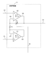
- FIG. 12 shows an internal circuit of the differential amplifier 11.
- the differential amplifier 11 includes two operational amplifiers 60 and 61 and reference resistors R1 and R2.
- the reference resistor R2 is composed of a variable resistor, and the resistance value of the reference resistor R2 can be changed by the control signal 28.
- the positive input of the operational amplifier 60 is connected to one of the terminals 22 of the magnetic field detection element 10.
- the + input of the operational amplifier 61 is connected to the terminal 21 of the magnetic field detection element 10.
- the negative input 67 of the operational amplifier 61 and the output 68 of the operational amplifier 61 are short-circuited.
- the output 68 is connected to one side of the reference resistor R1.
- the other end of the reference resistor R1 is connected to the negative input 65 of the operational amplifier 60 and one terminal of the reference resistor R2.
- the other terminal of the reference resistor R2 is connected to the output 66 and the output 25 of the operational amplifier 60.
- the reference resistor R2 is a variable resistor
- the reference resistor R1 may be a variable resistor instead.
- the output 25 of the differential amplifier 11 is connected to the + input of the comparator 12 in FIG. 1, and the output 26 of the voltage variable circuit 13 is connected to the ⁇ input of the comparator 12.
- the output 27 indicates H (1)
- the output 26 is greater than the output 25, the output 27 indicates L (0).
- the sample variation correction algorithm (S110) in FIG. 4A will be described.
- the difference voltage between Vp and Vn in the non-magnetic state is as close to 0V as possible for the sake of simplicity.
- the output 25 is approximately VDD / 2 because the second item of VDD / 2 + (Vp ⁇ Vn) ⁇ (R2 / R1 + 1) is 0 in the absence of a magnetic field.
- VDD / 2 is shown as voltage A in FIG.
- the output 26 of the voltage variable circuit 13 becomes an arbitrary voltage value based on the internal resistance division by the digital value set in the register 4B.
- the CPU 15 initializes the output 26 of the voltage variable circuit 13 to VSS by writing 00 in the register 4B.
- the output 25 indicates VDD / 2 in the absence of a magnetic field (S111). Therefore, the output 27 of the comparator 12 is H. At this time, until the output 27 of the comparator 12 becomes L (Yes in S112), the CPU 15 increments the digital setting value of the register 4B of the voltage variable circuit 13 (S113) and repeats the comparison operation.
- the output 27 of the comparator 12 becomes L.
- the CPU 15 holds the value of the register 4B of the voltage variable circuit 13 at this time as an initial value N in the ROM 16 (S114). This value is due to process variation and varies from sample to sample. Therefore, by writing this value into the ROM 16 and reading it out when necessary, it can be applied to later sample variation correction.
- the output 27 of the comparator 12 indicates L.
- the magnetic field X [mT] is applied to the magnetic field detection element 10 (S121)
- the magnetic field X [mT] Accordingly, the difference voltage between Vp and Vn increases.
- the output 25 is amplified by (Vp ⁇ Vn) ⁇ (R2 / R1 + 1).
- the amplified voltage is added to the output voltage (voltage A (VDD / 2)) of the differential amplifier 11 at the initial value N to become a voltage B (see FIG. 5).
- the CPU 15 similarly increments the digital setting value of the register 4B of the voltage variable circuit 13 (S123) until the output 27 of the comparator 12 becomes L (Yes in S124), and repeats the comparison operation. .
- FIG. 5 shows that the value of the register 4B is 7A (S125).
- the digital value obtained by subtracting one or more from the value (7A) of the register 4B of the voltage variable circuit 13 is held in the ROM 16 as X1-1 (S126).
- the magnetic field Y determination process (S130) as the magnetic field detection Y determination algorithm in FIG. 4D, the same process as the magnetic field X determination process (S120) is performed. That is, the magnetic field Y [mT] is applied to the magnetic field detection element 10 (S131), the digital setting value of the register 4B of the voltage variable circuit 13 is incremented (S134), and the comparison operation (S134) is repeated.
- FIG. 5 shows that the value of the register 4B is 7C (S135).
- the CPU 15 holds a digital value obtained by subtracting one or more from the value (7C) of the register 4B of the voltage variable circuit 13 at this time as Y1-1 in the ROM 16 (S136).
- the magnetic field Z determination process (S140) as the magnetic field detection Z determination algorithm, the same processes as the magnetic field X determination process and the magnetic field Y determination process are performed. That is, the magnetic field Z [mT] is applied to the magnetic field detection element 10 (S141). Processing in steps S142 to S145 is performed. As a result, Z1-1 is held in the ROM 16 (S146).
- the values X1-1, Y1-1, and Z1-1 written in the ROM 16 are written in the register 4B by a microcomputer program when detecting the application of the magnetic field, and the output 26 of the voltage variable circuit 13 detects the values. Can be set to any voltage.
- the magnetic field application determination table shown in FIG. 2A is written in the ROM 16. Therefore, for example, when it is desired to detect the magnetic field X, as shown in the operation shown in FIG.
- the output 27 of the device 12 becomes H (S14). Thereby, CPU15 can determine the presence or absence of a magnetic field.
- the setting value of the magnetic field detection can be reliably written in the ROM 16 for each sample. Therefore, sample variation is reduced, and the CPU 15 can detect a plurality of magnetic field strengths X [mT], Y [mT], and Z [mT].
- the magnetic field detection setting algorithm shown in FIGS. 4A to 4E is executed on the microcomputer (magnetic field detection microcomputer 19) mounted on the set to reduce the magnetic field detection level error for each sample and reliably detect the magnetic field. And a plurality of magnetic field strength levels can be detected. Furthermore, as a magnetic field detection microcomputer, the magnetic field detection setting algorithm shown in FIGS. 4A to 4E can be executed at the time of microcomputer shipment inspection to function at the time of microcomputer shipment. That is, the processes of FIGS. 4A to 4E are performed as a magnetic field detection setting algorithm at the time of microcomputer shipment inspection for mounting the magnetic field input determination table. In this case, it is particularly effective because the trouble of dealing with the set side incorporating the microcomputer (magnetic field detection microcomputer) can be saved.
- the magnetic field detection setting algorithm shown in FIGS. 4A to 4E is executed at the time of microcomputer inspection, there are the following merits.
- a shipment inspection of a semiconductor chip is often inspected at any one of a plurality of temperature conditions such as a low temperature, a normal temperature, and a high temperature in order to ensure that the semiconductor chip operates within a predetermined temperature range.
- the digital value set in the register 4B for detecting the magnetic field X [mT] is X1-1, which is one or more values lower than X1.
- the voltage dividing ratio is always substantially constant regardless of the temperature. Further, it is not necessary to compensate for the temperature according to the temperature characteristics of the magnetic field detecting element 10.
- the magnetic field detection element 10 it is assumed that the magnetic field sensitivity is lower at a low temperature than at a normal temperature.
- the magnetic field detection setting algorithm shown in FIG. 4A to FIG. 4E is executed at the time of microcomputer shipment inspection under the temperature condition (high temperature in this description) where the output voltage B becomes lowest when a magnetic field is applied.
- the magnetic field detection setting algorithm shown in FIGS. 4A to 4E is executed under the temperature condition where the magnetic field sensitivity becomes weak, so that more accurate magnetic field detection can be realized. .
- the magnetic field detection microcomputer includes a magnetic field detection element 10 for detecting a magnetic field, a differential amplifier 11 that amplifies the output voltage of the magnetic field detection element 10, and a voltage control signal (control signal). 29), the voltage variable circuit 13 that generates a variable reference voltage, the comparator 12 that compares the output of the differential amplifier 11 with the reference voltage generated by the voltage variable circuit 13, and the voltage variable circuit.
- a voltage control register (register 4B) that holds a voltage control value for controlling the level of the reference voltage generated by the signal and outputs a voltage control signal (control signal 29) having the voltage control value to the voltage variable circuit 13;
- the magnetic field strength which is the strength of the magnetic field applied to the magnetic field detecting element 10
- the voltage control value corresponding to the magnetic field to be detected is set in the storage unit (ROM 16) preliminarily stored as the first table and the voltage control register, and the voltage control value is determined from the comparison result of the comparator 12 and the first table.
- a CPU 15 for determining the presence or absence of the magnetic field intensity corresponding to.
- the voltage control value and the magnetic field strength are stored in advance in the storage unit (ROM 16), and the voltage control value corresponding to the magnetic field to be detected is set in the voltage control register (register 4B).
- the presence or absence of the magnetic field intensity corresponding to the voltage control value can be determined. That is, the presence or absence of the magnetic field intensity corresponding to the voltage control value can be easily determined.
- the conventional voltage variable circuit is configured to generate two types of reference voltages.
- the voltage variable circuit 13 of the magnetic field detection microcomputer 19 in the present embodiment is configured to generate one reference voltage (output 26). Therefore, the configuration of the voltage variable circuit 13 can be simplified.
- the magnetic field detection microcomputer 19 in the present embodiment does not require a voltage variable circuit having a complicated configuration, and can easily determine the presence or absence of magnetic field strength. That is, the magnetic field detection microcomputer 19 can easily determine the presence or absence of the magnetic field strength using the voltage variable circuit 13 having a simple configuration.
- the storage unit (ROM 16) By previously storing the voltage control value and the magnetic field strength in the storage unit (ROM 16), it is possible to easily determine the presence or absence of the magnetic field strength corresponding to the voltage control value. In addition, a complicated analog circuit is not required, and the characteristic variation of the sensor (magnetic field detection element 10) can be easily reduced.
- the differential amplifier 11 is variable in gain according to the gain control signal. That is, the gain (amplification degree) of the output of the differential amplifier 11 is switched according to the gain control value of the gain control signal.
- the magnetic field detection microcomputer 19 further includes a gain control register (register 4A) that holds a gain control value and outputs a gain control signal (control signal 28) having the gain control value to the differential amplifier 11. Also good.
- the first table is stored in the ROM 16 and previously stores the magnetic field strength and the voltage control value for each gain control value.
- the CPU 15 sequentially increases or decreases the voltage control value held in the voltage control register (register 4B), and the magnetic field intensity corresponding to the voltage control value when the output of the comparator is inverted. Is read from the first table as the detected magnetic field strength.
- the CPU 15 holds a value stored in the voltage control register (register 4B) in a state where a known magnetic field (eg, no magnetic field, magnetic field X, Y, or Z) is applied to the magnetic field detection element 10.
- a known magnetic field eg, no magnetic field, magnetic field X, Y, or Z
- the value of the register 4B immediately before or after the inversion is stored in the first table (table of FIG. 2A) as a voltage control value corresponding to the known magnetic field.
- the table in FIG. 2B (second table) and the table in FIG. 2C can be created in the same manner.
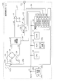
- FIG. 6 is a block diagram of the magnetic field detection microcomputer 19A according to the second embodiment of the present invention.
- the voltage variable circuit 13 is replaced with a DAC 50 as compared with the magnetic field detection microcomputer 19 of FIG.
- the DAC 50 is a D / A converter. That is, the voltage variable circuit 13 may be a D / A converter (DAC 50).
- the DAC 50 generates an output 51 as a reference voltage.
- the output 51 of the DAC 50 is connected to the input of the analog output selection circuit 54.
- the analog output selection circuit 54 is connected to a control signal 55 for selecting one of the outputs 26 and 52.
- the control signal 55 is connected to the register 4D.
- the output 52 is connected as a DAC output terminal to a pad 53 serving as a signal extraction port on the semiconductor chip of the microcomputer.
- the value of the register 4D can be arbitrarily set by a program of the microcomputer, and the output 51 of the DAC 50 can be output to the DAC output terminal (pad 53). .
- the output 51 of the DAC 50 can be output as the output 26. Therefore, an analog output corresponding to an arbitrary digital code can be output to the terminal by a program of the microcomputer and functions as a DAC.
- the magnetic field can be detected.
- a DAC is originally built in a microcomputer as a general purpose.
- this embodiment is applied to a DAC built-in microcomputer, the voltage variable circuit 13 becomes unnecessary, and the chip area can be reduced.
- the DAC 50 incorporated in the microcomputer generally has an 8-bit resolution or more.
- the potential of the output 26 of the analog output selection circuit 54 can be set with high accuracy over a wide range from GND to VDD based on the algorithm of FIGS. 4A to 4E.
- the DAC 50 with built-in microcomputer can be used in a time-sharing manner by programmatically executing output to the pad 53 as a DAC output terminal and output to the output 26 as magnetic field detection according to the system application. I can do it. Therefore, the voltage variable circuit 13 is not required, and a minimum and highly accurate magnetic field detection microcomputer is provided.
- the output 25 of FIG. 6 generates a potential of VDD / 2 + (Vp ⁇ Vn) ⁇ (R2 / R1 + 1).
- the output 26 generates the potential of the output of the DAC 50 ((VDD / (2 n ⁇ 1)) ⁇ DAC set value).
- n is n of n-bitDAC.
- the magnetic field detection microcomputer 19A can easily set the magnetic field detection with the DAC setting value based on Equation 1 for a plurality of magnetic field strengths. As a result, a complicated analog circuit or the like for performing magnetic field detection is not required.
- the DAC set value can be set for each sample by the algorithm shown in FIG. Therefore, process variation for each sample can be reduced, and a plurality of magnetic field detections can be realized reliably and easily.
- the magnetic field detection microcomputer according to the present embodiment is the magnetic field detection microcomputer 19 according to the first embodiment.
- the magnetic field detection microcomputer 19 stores in advance the magnetic field intensity of the south pole applied to the magnetic field detection element 10 and a voltage control value indicating a condition for inverting the output of the comparator 12.
- the first table (the table in FIG. 2A) stores in advance the magnetic field intensity of the N pole applied to the magnetic field detection element 10 and a voltage control value indicating a condition that the output of the comparator 12 is inverted.
- the CPU 15 alternately performs magnetic field detection using the first table and magnetic field detection using the second table (the table in FIG. 2B) a predetermined number of times.
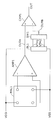
- FIG. 7 shows the relationship between a microcomputer incorporating a magnetic field detection element and a magnet, and a magnetic field is applied perpendicular to the plane of the microcomputer as a microcomputer chip.
- the microcomputer corresponds to a magnetic field detection microcomputer (for example, the magnetic field detection microcomputer 19) described in each embodiment.
- the magnetic field detection microcomputer 19 stores in advance the magnetic field intensity of the south pole applied to the magnetic field detection element 10 and a voltage control value indicating a condition for inverting the output of the comparator 12.
- the first table used in the present embodiment (the table in FIG. 2A) is configured to preliminarily store the magnetic field intensity of the N pole applied to the magnetic field detection element and a voltage control value indicating a condition for inverting the output of the comparator.
- N and S poles of the magnet are also simply referred to as the N and S poles.
- FIG. 8 shows a setting algorithm and an operation timing chart of the positive magnetic field detection when approaching the N pole side with respect to the microcomputer.
- the magnetic field detection determination table of FIG. 2A is created.
- the N pole is close to the microcomputer, a potential difference of Vp> Vn is generated. Therefore, a voltage higher than VDD / 2 is generated at the output 25 when the second term of the equation VDD / 2 + (Vp ⁇ Vn) ⁇ (R2 / R1 + 1) becomes positive.
- the detection level algorithm in the present embodiment is the same as that described in FIG. That is, if the output voltage (output 51) of the DAC 50 for detecting the magnetic field X [mT] is determined, the comparator 12 is applied in accordance with the application of the magnetic field and the magnetic field X [mT] as shown in FIG. The output X1-1 can be determined.
- FIG. 9 shows a setting algorithm for detecting the negative magnetic field when the S pole side is brought close to the microcomputer.
- the magnetic field detection determination table of FIG. 2B is created.
- FIG. 9 is equivalent to applying negative polarity -X [mT] to application of positive polarity X [mT] in FIG.
- Vp ⁇ Vn a potential difference of Vp ⁇ Vn is generated. Therefore, the second term of the equation VDD / 2 + (Vp ⁇ Vn) ⁇ (R2 / R1 + 1) is negative. Therefore, a voltage lower than VDD / 2 is generated at the output 25.
- the output voltage of the differential amplifier 11 when the magnetic field ⁇ X is applied to the magnetic field detecting element 10 becomes the voltage ⁇ B.
- the CPU 15 decrements the digital setting value of the register 4B of the voltage variable circuit 13 and repeats the comparison operation until the output 27 of the comparator 12 becomes H.
- the CPU 15 holds a digital value (that is, a value immediately after) obtained by adding one or more from the value of the register 4B of the voltage variable circuit 13 at this time in the ROM 16 as -X1 + 1.
- the CPU 15 responds to the application of no magnetic field and magnetic field -X [mT] to the magnetic field detection element 10 as shown in FIG.
- the N / S pole can be determined from the output 27 of the comparator 12.
- the N pole / S pole application determination microcomputer execution sequence will be described with reference to FIGS.
- the CPU 15 holds the value of X1-1 written in the ROM 16 in the register 4B (S11), and based on the operation shown in FIG. The X magnetic field is determined.
- the CPU 15 holds the value of ⁇ X1 + 1 written in the ROM 16 in the register 4B, and determines the ⁇ X magnetic field in the same manner as the operation shown in FIG. .
- the microcomputer program is executed in a time division manner. That is, the CPU 15 alternately performs magnetic field detection using the first table and magnetic field detection using the second table for each predetermined number of times.
- the CPU 15 can determine whether or not the N / S magnetic field is applied to the magnetic field detection element 10 (microcomputer).
- the time division timing frequency can be set optimally by the program according to the required set specifications.
- 10 shows a state where the switches 30 and 31 of the magnetic field detecting element 10 are turned off. By turning off the power, the current flowing through the magnetic field detection element 10 is reduced.
- the present embodiment it is possible to detect the direction of the vertical magnetic field (N pole / S pole) on the semiconductor substrate and to detect a plurality of desired magnetic field strengths.
- FIG. 13 is a block diagram of a magnetic field detection microcomputer 19B according to Embodiment 4 of the present invention.
- the magnetic field detection microcomputer 19B in the present embodiment selects the booster circuit 100 that boosts the power supply voltage, one of the boosted power supply voltage and the power supply voltage that is not boosted, and supplies the selected power supply voltage to the magnetic field detection element.
- the voltage switching circuit 104 is provided.
- the first table (the table in FIG. 2A) stores in advance the magnetic field strength and the voltage control value corresponding to each of the boosted power supply voltage and the unboosted power supply voltage.
- the CPU 15 detects the magnetic field strength using a voltage control value corresponding to the power supply voltage selected by the voltage switching circuit 104.
- the magnetic field detection microcomputer 19B further includes a booster circuit 100 and a voltage switching circuit 104 as compared with the magnetic field detection microcomputer of FIG.
- the booster circuit 100 boosts the power supply voltage.
- a power supply VDD is connected to a boost reference potential 101, and an output 102 as an output signal after boosting is connected to one input of the voltage switching circuit 104.
- the input 103 of the voltage switching circuit 104 is connected to VDD.
- the voltage switching circuit 104 outputs either the output 102 or the input 103 as the output 105 in accordance with the control signal 106. That is, the voltage switching circuit 104 selects one of the boosted power supply voltage and the non-boosted power supply voltage, and supplies the selected power supply voltage to the magnetic field detection element.
- the control signal 106 is connected to the register 4E. A value can be arbitrarily set in the register 4E by the CPU 15.
- the booster circuit 100 is generally a microcomputer with a built-in LCD display function, and has an LCD booster circuit for driving the LCD.
- the booster circuit 100 may also be used as the LCD booster circuit.
- the output 102 has a potential of k ⁇ VDD.
- a selection value is set in the register 4E by the program of the microcomputer.
- the difference voltage between the terminal 21 and the terminal 22 increases in proportion to the applied power supply voltage.
- the output 25 is k ⁇ VDD / 2 + h (Vp ⁇ Vn) ⁇ (R2 / R1 + 1) according to Equation 1. Therefore, the output 25 (output voltage) is increased by the factor of h. This is particularly effective when detecting a minute magnetic field.
- the CPU 15 sets the DAC 50 value (DAC setting value) so that the following Expression 2 is satisfied when the magnetic field ⁇ X [mT] is applied.
- the CPU 15 can detect a minute magnetic field ⁇ X [mT]. That is, the CPU 15 detects the magnetic field strength using the voltage control value corresponding to the power supply voltage selected by the voltage switching circuit 104.
- FIG. 14 is a perspective view of a semiconductor substrate 200 used in the magnetic field detection microcomputer according to the fifth embodiment of the present invention.
- the magnetic field detection microcomputer according to the fifth embodiment may be any one of the magnetic field detection microcomputers 19, 19A, and 19B.
- the magnetic field detection element 10, the differential amplifier 11, the voltage variable circuit 13, the comparator 12, the voltage control register (register 4B), the storage unit (ROM 16), and the CPU 15 are on the same semiconductor substrate 200. Is formed.
- FIG. 14 shows only some of the components formed on the semiconductor substrate 200 among all the components included in the magnetic field detection microcomputer.
- FIG. 14 does not show the differential amplifier 11, the voltage variable circuit 13, the comparator 12, the register 4B, the ROM 16, the CPU 15, and the like.
- the semiconductor substrate 200 is a P-type substrate.
- the semiconductor substrate 200 is not limited to a P-type substrate and may be an N-type substrate.
- the magnetic field detection element 10 is formed on the semiconductor substrate 200.
- Nwells 201 and 202 are formed on the semiconductor substrate 200.
- Terminals 21, 22, 23, and 24 are formed at four corners of the Nwell 201.
- the terminals 21, 22, 23, and 24 function as electrode outlets.
- the magnetic field detection element 10 as a Hall element is formed on the semiconductor substrate 200. That is, the magnetic field detection element 10 is a Hall element.
- Nwell 202 a P-type doped source 203, drain 205, and gate 204 are formed as P-channel transistors.
- an N-type doped source 208, drain 206, and gate 207 are formed on the semiconductor substrate 200 as N-channel transistors.
- the Nwell 202 forming the P-channel transistor and the Nwell 201 forming the Hall element are the same Nwell.
- Nwell 202 is an Nwell that forms a fine CMOS, and the concentration of Nwell 202 is a concentration suitable for a fine process.
- the sensitivity of the Hall element is proportional to the carrier mobility ⁇ , and the lower the Nwell concentration, the higher the carrier mobility ⁇ . Therefore, in order to increase the sensitivity of the Hall element, the concentration of Nwell is appropriately adjusted so that the carrier mobility ⁇ increases in the single Hall element and the single Hall IC.
- the Hall element when the Hall element is formed by the same substrate and the same fine CMOS process as the microcomputer, it must be formed at the concentration of Nwell formed by the fine CMOS. Therefore, it is generally difficult to increase the sensitivity of the built-in Hall element (magnetic field detecting element 10) than the single Hall element and the single Hall IC using an optimal process.
- the resistance of the reference resistor R2 can be varied by the control signal 28 to the differential amplifier 11. By doing so, the amplification factor of the differential amplifier 11 can be improved.
- sample variation can be reduced by arbitrarily setting the control signal 29 of the voltage variable circuit 13 by a microcomputer program.
- the booster circuit 100 can increase the sensitivity of the Hall element (magnetic field detection element 10), and can reduce variations in temperature characteristics during microcomputer shipment inspection. Therefore, even if Nwell on a fine CMOS is used, the magnetic field detection can be reliably realized by compensating for the decrease in magnetic field sensitivity.
- non-volatile flash microcomputers often have higher voltage transistors than ordinary volatile CMOS mask ROM microcomputers. In that case, it is more effective to form the Hall element using the Nwell that increases the sensitivity of the Hall element, that is, the Nwell that forms the high breakdown voltage element that increases the carrier mobility ⁇ .
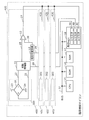
- FIG. 15 is a semiconductor layout diagram of the magnetic field detection microcomputer according to the sixth embodiment of the present invention. Each component shown in FIG. 15 is formed on a semiconductor substrate 200.
- Hall element portions 300, 301, 302, and 303 are formed.
- Each of the Hall element units 300, 301, 302, and 303 is a portion (region) where the magnetic field detection element 10 as the Hall element of FIG. 14 is formed.
- IO cells 305, 306, 307, 308, 309, 310, 311, 312, 313 are arranged in regions 314, 315, 316, 317 sandwiched between the Hall element units 300, 301, 302, 303. .
- a pad 304 is disposed in each of the IO cells 305, 306, 307, 308, 309, 310, 311, 312, 313.
- An area surrounded by the areas 314, 315, 316, and 317 is a circuit area in which the ROM 16, the RAM 17, the peripheral logic 18, and the like are formed.
- the circuit area is a circuit area composed of standard cells.
- the 16 further shows the power supply line 352 and the power supply line 353 of the IO cells 308 and 309 as compared with FIG.
- the power supply line 352 is a line for supplying the voltage VDD.
- the power supply line 352 is a line for supplying the voltage VSS.
- the power supply line 352 and the power supply line 353 are connected as power supplies for the IO cells 308 and 309.
- the power supply line 352 and the power supply line 353 are arranged so as not to intersect with the terminals 21, 22, 23, and 24 of the Hall element unit 301.
- FIG. 16 shows the Nwell 201 of the Hall element unit 301, the Nwell 354 of the IO cell 305, and the Nwell 355 of the IO cell 309.
- the corner cell areas sandwiched between the IO cell 308 and the IO cell 309 are generally empty areas only with the power supply lines 352 and 353 disposed therein.
- the magnetic field detection element 10 can be configured in the Hall element unit 301.
- the magnetic field detection element 10 of FIG. 1 when the magnetic field detection element 10 of FIG. 1 is formed by a Hall element, the magnetic field detection element 10 can be arranged on one chip without increasing the area of the Hall element, thereby realizing cost reduction. I can do it.
- the Hall element magnetic field detection element 10
- the microcomputer operates. It is less affected by noise and is effective.
- the magnetic field detection elements 10 as Hall elements are formed at the four corners of the semiconductor substrate 200.
- the Hall element is not limited to all four corners of the semiconductor substrate 200, and may be formed only at one of the four corners of the semiconductor substrate 200, for example. That is, the magnetic field detection element 10 as the Hall element is formed in at least one of the four corners of the semiconductor substrate 200.
- FIG. 17 is a block diagram of a magnetic field detection microcomputer 405 according to Embodiment 7 of the present invention.
- the magnetic field detection microcomputer 405 includes magnetic field detection circuit blocks 400, 401, 402, 403, a CPU 15, a ROM 16, a RAM 17, and a peripheral logic 18.
- the magnetic field detection circuit block 400 includes a magnetic field detection element 10 as a Hall element, a differential amplifier 11, a comparator 12, a voltage variable circuit 13, and control signals 28 and 29 shown in FIG.
- the connection configuration of the magnetic field detection element 10, the differential amplifier 11, the comparator 12, the voltage variable circuit 13, and the like is the same as the connection configuration in FIG.
- each of the magnetic field detection circuit blocks 401, 402, and 403 is the same as the configuration of the magnetic field detection circuit block 400.
- the magnetic field detection microcomputer 405 includes, in addition to the magnetic field detection circuit block 401, three magnetic field detection elements 10 having the same configuration as the magnetic field detection element 10, the differential amplifier 11, the voltage variable circuit 13, and the comparator. 3 sets having the same configuration as the set including 12.
- the CPU 15 detects a magnetic field using each of the four sets (magnetic field detection circuit blocks 400, 401, 402, and 403).
- Magnetic field detection circuit blocks 400, 401, 402, and 403 include Hall element units 300, 301, 302, and 303, respectively.
- the output of the Hall element unit 300 corresponds to the output 27.
- the outputs of the Hall element units 301, 302, and 303 correspond to the output 410, the output 420, and the output 430, respectively.
- Hall element units 300, 301, 302, and 303 are arranged at the four corners of semiconductor substrate 200 as described with reference to FIG.
- the magnetic field detection element 10 is formed in each of the Hall element units 300, 301, 302, and 303. That is, the four magnetic field detecting elements 10 are disposed at the four corners of the semiconductor substrate 200.
- the Hall element units 300, 301, 302, and 303 are arranged in the four corner corner cells that are empty areas on the semiconductor substrate 200. Thereby, the area for arrange
- the CPU 15 can sensitively detect the direction of the magnetic field.
- the output 27, the output 410, the output 420, and the output 430 in FIG. 18 correspond to the outputs 27, 410, 420, and 430 in the Hall element units 300, 301, 302, and 303 in FIGS.
- FIG. 19 additionally shows magnetic field directions (directions) YL, XR, YR, and XL with respect to FIG.
- the direction of the magnetic field is the magnetic field YL direction shown in FIG.
- the direction of the magnetic field is the magnetic field XR direction shown in FIG.
- the direction of the magnetic field is the magnetic field YR direction shown in FIG.
- the direction of the magnetic field is the magnetic field XL direction shown in FIG.
- the direction of the magnetic field appears as a phase on the time axis due to the strength of the vertical magnetic field on the Hall element surface.
- the CPU 15 can detect the magnetic field directions (orientations) YL, XR, YR, and XL by microcomputer control.
- an optimum detection state can be set by setting the booster circuit 100, the amplification degree of the differential amplifier 11, and the voltage variable circuit 13 to optimum values by the microcomputer program when detecting the magnetic field. .
- the area for arranging the Hall element portion can be reduced, and a microcomputer-mixed one-chip implementation with the Hall element can be realized by an existing microcomputer process. That is, in an existing microcomputer manufacturing process, a microcomputer-mixed one-chip implementation with a Hall element can be realized.
- the direction of the magnetic field in the horizontal direction of the semiconductor substrate (X direction on the upper side of the chip IO, Y direction on the left side of the chip IO, X direction on the lower side of the chip IO, and Y direction on the right side of the chip IO) can be detected.
- a detection microcomputer can be provided. That is, it is possible to reduce the offset error of the Hall element for each sample, the temperature characteristic, and the like with a minimum area and low cost.
- the chip size is particularly effective because the square is a uniform condition for the Hall elements at the four corners. That is, the shape of the semiconductor substrate 200 is preferably a square.
- the sample variation error of the sensor can be reduced by a minimum means. Further, it is possible to detect the direction of the vertical magnetic field (N pole / S pole) on the semiconductor substrate 200 and to detect a plurality of desired magnetic field strength levels. Moreover, the area for arranging the Hall element portion can be reduced, and a microcomputer-mixed one-chip integration with the Hall element can be realized by an existing microcomputer process. Further, the direction of the horizontal magnetic field of the semiconductor substrate 200 (X direction on the upper side of the chip IO, Y direction on the left side of the chip IO, X direction on the lower side of the chip IO, and Y direction on the right side of the chip IO) can be detected. A magnetic field detection microcomputer can be provided.
- FIG. 20 is a block diagram showing a characteristic functional configuration of the magnetic field detection microcomputer 500.
- the magnetic field detection microcomputer 500 corresponds to any one of the above-described magnetic field detection microcomputers 19, 19A, 19B, and 405. That is, FIG. 20 is a block diagram showing main functions related to the present invention among the functions of any one of the magnetic field detection microcomputers 19, 19A, 19B, and 405.
- the magnetic field detection microcomputer 500 includes a magnetic field detection element 510, a differential amplifier 520, a voltage variable circuit 530, a comparator 540, a voltage control register 550, a storage unit 560, and a CPU 570.
- the magnetic field detection element 510 is an element for detecting a magnetic field.
- the magnetic field detection element 510 corresponds to the magnetic field detection element 10.
- the differential amplifier 520 amplifies the output voltage of the magnetic field detection element 510.
- the differential amplifier 520 corresponds to the differential amplifier 11.
- the voltage variable circuit 530 generates a variable reference voltage according to the voltage control signal (control signal 29).
- the voltage variable circuit 530 corresponds to the voltage variable circuit 13 or the DAC 50.
- the comparator 540 compares the output of the differential amplifier 520 with the reference voltage generated by the voltage variable circuit 530. Then, the comparator 540 outputs the comparison result.
- the comparator 540 corresponds to the comparator 12.
- the comparison result output from the comparator 540 corresponds to the output 27.
- the voltage control register 550 holds a voltage control value and outputs the voltage control signal having the voltage control value to the voltage variable circuit 530.
- the voltage control value is a value for controlling the level of the reference voltage generated by the voltage variable circuit.
- the voltage control register 550 corresponds to the register 4B.
- the storage unit 560 includes a magnetic field strength that is a magnetic field strength applied to the magnetic field detection element 510 and the voltage control value immediately before or immediately after the output of the comparator 540 is inverted when the voltage control value is increased or decreased. Are stored in advance as a first table.
- the storage unit 560 corresponds to the ROM 16.
- the first table corresponds to, for example, the magnetic field detection determination table in FIG. 2A.
- the CPU 570 sets a voltage control value corresponding to the magnetic field to be detected in the voltage control register 550. Further, the CPU 570 determines the presence / absence of the magnetic field intensity corresponding to the voltage control value from the comparison result of the comparator 540 and the first table. The CPU 570 corresponds to the CPU 15.
- the differential amplifier 520, the voltage variable circuit 530, the comparator 540, the voltage control register 550, the storage unit 560, and the CPU 570 included in the magnetic field detection microcomputer 500 are all or part of one LSI (Large Scale Integration: large scale). (Integrated circuit) or the like.
- the present invention may be realized as a magnetic field detection method in which the operations of characteristic components included in the magnetic field detection microcomputer according to each of the above embodiments are used as steps.
- the present invention may be realized as a program that causes a computer to execute each step included in such a magnetic field detection method.
- the present invention may be realized as a computer-readable recording medium that stores such a program.
- the program may be distributed via a transmission medium such as the Internet.
- the present invention is useful as a magnetic field detection microcomputer that can easily determine the presence or absence of magnetic field strength without requiring a voltage variable circuit having a complicated configuration.
Landscapes
- Physics & Mathematics (AREA)
- General Physics & Mathematics (AREA)
- Condensed Matter Physics & Semiconductors (AREA)
- Engineering & Computer Science (AREA)
- Theoretical Computer Science (AREA)
- Databases & Information Systems (AREA)
- Mathematical Physics (AREA)
- Software Systems (AREA)
- General Engineering & Computer Science (AREA)
- Data Mining & Analysis (AREA)
- Measuring Magnetic Variables (AREA)
- Hall/Mr Elements (AREA)
- Geophysics And Detection Of Objects (AREA)
Abstract
Priority Applications (3)
| Application Number | Priority Date | Filing Date | Title |
|---|---|---|---|
| JP2012526280A JP5514314B2 (ja) | 2010-07-30 | 2011-06-30 | 磁界検知マイコンおよび磁界検知方法 |
| CN201180033356.XA CN102971640B (zh) | 2010-07-30 | 2011-06-30 | 磁场检测微型计算机及磁场检测方法 |
| US13/750,589 US9316702B2 (en) | 2010-07-30 | 2013-01-25 | Magnetic-field detection microcomputer and magnetic-field detecting method |
Applications Claiming Priority (2)
| Application Number | Priority Date | Filing Date | Title |
|---|---|---|---|
| JP2010-173025 | 2010-07-30 | ||
| JP2010173025 | 2010-07-30 |
Related Child Applications (1)
| Application Number | Title | Priority Date | Filing Date |
|---|---|---|---|
| US13/750,589 Continuation US9316702B2 (en) | 2010-07-30 | 2013-01-25 | Magnetic-field detection microcomputer and magnetic-field detecting method |
Publications (1)
| Publication Number | Publication Date |
|---|---|
| WO2012014376A1 true WO2012014376A1 (fr) | 2012-02-02 |
Family
ID=45529615
Family Applications (1)
| Application Number | Title | Priority Date | Filing Date |
|---|---|---|---|
| PCT/JP2011/003762 WO2012014376A1 (fr) | 2010-07-30 | 2011-06-30 | Micro-ordinateur destiné à détecter un champ magnétique, et procédé de détection d'un champ magnétique |
Country Status (4)
| Country | Link |
|---|---|
| US (1) | US9316702B2 (fr) |
| JP (1) | JP5514314B2 (fr) |
| CN (1) | CN102971640B (fr) |
| WO (1) | WO2012014376A1 (fr) |
Cited By (2)
| Publication number | Priority date | Publication date | Assignee | Title |
|---|---|---|---|---|
| JP2017049217A (ja) * | 2015-09-04 | 2017-03-09 | 旭化成エレクトロニクス株式会社 | 磁気検出装置及び方法ならびに集積回路 |
| JP2020025302A (ja) * | 2014-07-07 | 2020-02-13 | アセンシア・ディアベティス・ケア・ホールディングス・アーゲー | 兼用圧電音響部品および振動センサによる改善されたデバイスペアリングのための方法および装置 |
Families Citing this family (4)
| Publication number | Priority date | Publication date | Assignee | Title |
|---|---|---|---|---|
| JP6393470B2 (ja) * | 2013-10-23 | 2018-09-19 | 日立オートモティブシステムズ株式会社 | センサ装置 |
| US10386392B2 (en) | 2015-01-28 | 2019-08-20 | Hioki Denki Kabushiki Kaisha | Hall element driving circuit, sensor circuit, and current measuring apparatus |
| US10360855B2 (en) * | 2015-08-17 | 2019-07-23 | Semiconductor Energy Laboratory Co., Ltd. | Semiconductor device, display panel, and electronic device |
| US9852094B2 (en) * | 2015-12-07 | 2017-12-26 | Allegro Microsystems, Llc | Device configuration using a magnetic field |
Citations (4)
| Publication number | Priority date | Publication date | Assignee | Title |
|---|---|---|---|---|
| JPH03261869A (ja) * | 1990-03-13 | 1991-11-21 | Omron Corp | ホール素子の出力信号補正装置 |
| JP2006038799A (ja) * | 2004-07-30 | 2006-02-09 | Tamura Seisakusho Co Ltd | 検出器 |
| JP2006098306A (ja) * | 2004-09-30 | 2006-04-13 | Yamaha Corp | 磁気測定装置 |
| JP2009048539A (ja) * | 2007-08-22 | 2009-03-05 | Seiko Instruments Inc | 可変分圧回路及び磁気センサ回路 |
Family Cites Families (5)
| Publication number | Priority date | Publication date | Assignee | Title |
|---|---|---|---|---|
| JP2738605B2 (ja) * | 1991-06-04 | 1998-04-08 | 三菱電機株式会社 | 磁石発電装置 |
| FR2747822A1 (fr) * | 1996-04-17 | 1997-10-24 | Philips Electronics Nv | Systeme de lecture d'informations magnetiques muni d'un detecteur d'asperites thermiques |
| JP3912779B2 (ja) * | 2002-05-08 | 2007-05-09 | 松下電器産業株式会社 | 磁気式位置検出装置 |
| JP2008032424A (ja) * | 2006-07-26 | 2008-02-14 | Rohm Co Ltd | センサ回路、半導体装置、電子機器 |
| JP5144168B2 (ja) * | 2007-08-16 | 2013-02-13 | セイコーインスツル株式会社 | センサ回路 |
-
2011
- 2011-06-30 JP JP2012526280A patent/JP5514314B2/ja active Active
- 2011-06-30 CN CN201180033356.XA patent/CN102971640B/zh active Active
- 2011-06-30 WO PCT/JP2011/003762 patent/WO2012014376A1/fr active Application Filing
-
2013
- 2013-01-25 US US13/750,589 patent/US9316702B2/en active Active
Patent Citations (4)
| Publication number | Priority date | Publication date | Assignee | Title |
|---|---|---|---|---|
| JPH03261869A (ja) * | 1990-03-13 | 1991-11-21 | Omron Corp | ホール素子の出力信号補正装置 |
| JP2006038799A (ja) * | 2004-07-30 | 2006-02-09 | Tamura Seisakusho Co Ltd | 検出器 |
| JP2006098306A (ja) * | 2004-09-30 | 2006-04-13 | Yamaha Corp | 磁気測定装置 |
| JP2009048539A (ja) * | 2007-08-22 | 2009-03-05 | Seiko Instruments Inc | 可変分圧回路及び磁気センサ回路 |
Cited By (3)
| Publication number | Priority date | Publication date | Assignee | Title |
|---|---|---|---|---|
| JP2020025302A (ja) * | 2014-07-07 | 2020-02-13 | アセンシア・ディアベティス・ケア・ホールディングス・アーゲー | 兼用圧電音響部品および振動センサによる改善されたデバイスペアリングのための方法および装置 |
| US11399269B2 (en) | 2014-07-07 | 2022-07-26 | Ascensia Diabetes Care Holdings Ag | Device pairing taking into account at least one condition |
| JP2017049217A (ja) * | 2015-09-04 | 2017-03-09 | 旭化成エレクトロニクス株式会社 | 磁気検出装置及び方法ならびに集積回路 |
Also Published As
| Publication number | Publication date |
|---|---|
| JP5514314B2 (ja) | 2014-06-04 |
| JPWO2012014376A1 (ja) | 2013-09-09 |
| US9316702B2 (en) | 2016-04-19 |
| US20130138374A1 (en) | 2013-05-30 |
| CN102971640A (zh) | 2013-03-13 |
| CN102971640B (zh) | 2016-03-30 |
Similar Documents
| Publication | Publication Date | Title |
|---|---|---|
| JP5514314B2 (ja) | 磁界検知マイコンおよび磁界検知方法 | |
| TWI442206B (zh) | Voltage divider circuit and magnetic sensor circuit | |
| US9274179B2 (en) | Integrated sensor array with offset reduction | |
| GB2405701A (en) | Differential current sensing circuit | |
| US8278920B2 (en) | Magnetic sensor and magnetic measurement method | |
| US9322672B2 (en) | Magnetic sensor device | |
| US9267818B2 (en) | Magnetic sensor device | |
| JP5930252B2 (ja) | 擬似抵抗回路及び電荷検出回路 | |
| JP2007187509A (ja) | 容量式物理量センサ | |
| JP2008022457A (ja) | 半導体装置 | |
| US10816613B2 (en) | Magnetic sensor circuit | |
| TWI638145B (zh) | 感測電路及感測電路的控制方法 | |
| JP6158682B2 (ja) | 磁気センサ回路 | |
| JPH052037A (ja) | ゼロクロス検出回路 | |
| JP4641775B2 (ja) | 磁気検出用半導体集積回路およびそれを搭載した電子部品 | |
| US8207778B2 (en) | Physical quantity sensor | |
| JP2009284050A (ja) | 差動増幅回路 | |
| US10914618B2 (en) | Readout circuit for sensor and readout method thereof | |
| JP6580718B2 (ja) | バイアス電流回路、信号処理装置及びバイアス電流制御方法 | |
| JP2007040771A (ja) | ノイズ測定用半導体装置 | |
| US20220149856A1 (en) | Bridge sensor dc error cancellation scheme | |
| CN107591433B (zh) | 一种显示面板及其压力检测电路的压力检测方法、显示装置 | |
| CN114518486A (zh) | 一种输入失调电压的测量方法及电路 | |
| JP2013162493A (ja) | 入出力装置、半導体装置、電子機器、及びスイッチング制御方法 | |
| US11073493B2 (en) | Sensor device |
Legal Events
| Date | Code | Title | Description |
|---|---|---|---|
| WWE | Wipo information: entry into national phase |
Ref document number: 201180033356.X Country of ref document: CN |
|
| 121 | Ep: the epo has been informed by wipo that ep was designated in this application |
Ref document number: 11811983 Country of ref document: EP Kind code of ref document: A1 |
|
| WWE | Wipo information: entry into national phase |
Ref document number: 2012526280 Country of ref document: JP |
|
| NENP | Non-entry into the national phase |
Ref country code: DE |
|
| 122 | Ep: pct application non-entry in european phase |
Ref document number: 11811983 Country of ref document: EP Kind code of ref document: A1 |