WO2012011171A1 - エッチング装置 - Google Patents
エッチング装置 Download PDFInfo
- Publication number
- WO2012011171A1 WO2012011171A1 PCT/JP2010/062267 JP2010062267W WO2012011171A1 WO 2012011171 A1 WO2012011171 A1 WO 2012011171A1 JP 2010062267 W JP2010062267 W JP 2010062267W WO 2012011171 A1 WO2012011171 A1 WO 2012011171A1
- Authority
- WO
- WIPO (PCT)
- Prior art keywords
- electrode
- plasma
- stage
- outer peripheral
- etching apparatus
- Prior art date
- Legal status (The legal status is an assumption and is not a legal conclusion. Google has not performed a legal analysis and makes no representation as to the accuracy of the status listed.)
- Ceased
Links
Images





Classifications
-
- H—ELECTRICITY
- H01—ELECTRIC ELEMENTS
- H01J—ELECTRIC DISCHARGE TUBES OR DISCHARGE LAMPS
- H01J37/00—Discharge tubes with provision for introducing objects or material to be exposed to the discharge, e.g. for the purpose of examination or processing thereof
- H01J37/32—Gas-filled discharge tubes
- H01J37/32009—Arrangements for generation of plasma specially adapted for examination or treatment of objects, e.g. plasma sources
- H01J37/32082—Radio frequency generated discharge
- H01J37/32091—Radio frequency generated discharge the radio frequency energy being capacitively coupled to the plasma
-
- H—ELECTRICITY
- H01—ELECTRIC ELEMENTS
- H01J—ELECTRIC DISCHARGE TUBES OR DISCHARGE LAMPS
- H01J37/00—Discharge tubes with provision for introducing objects or material to be exposed to the discharge, e.g. for the purpose of examination or processing thereof
- H01J37/32—Gas-filled discharge tubes
- H01J37/32009—Arrangements for generation of plasma specially adapted for examination or treatment of objects, e.g. plasma sources
- H01J37/32082—Radio frequency generated discharge
- H01J37/321—Radio frequency generated discharge the radio frequency energy being inductively coupled to the plasma
-
- H—ELECTRICITY
- H01—ELECTRIC ELEMENTS
- H01J—ELECTRIC DISCHARGE TUBES OR DISCHARGE LAMPS
- H01J37/00—Discharge tubes with provision for introducing objects or material to be exposed to the discharge, e.g. for the purpose of examination or processing thereof
- H01J37/32—Gas-filled discharge tubes
- H01J37/32431—Constructional details of the reactor
- H01J37/32532—Electrodes
- H01J37/32568—Relative arrangement or disposition of electrodes; moving means
-
- H—ELECTRICITY
- H10—SEMICONDUCTOR DEVICES; ELECTRIC SOLID-STATE DEVICES NOT OTHERWISE PROVIDED FOR
- H10P—GENERIC PROCESSES OR APPARATUS FOR THE MANUFACTURE OR TREATMENT OF DEVICES COVERED BY CLASS H10
- H10P50/00—Etching of wafers, substrates or parts of devices
- H10P50/20—Dry etching; Plasma etching; Reactive-ion etching
- H10P50/24—Dry etching; Plasma etching; Reactive-ion etching of semiconductor materials
- H10P50/242—Dry etching; Plasma etching; Reactive-ion etching of semiconductor materials of Group IV materials
Definitions
- the technique disclosed in this specification relates to an etching apparatus that etches a workpiece using plasma.
- Patent Document 1 discloses an etching apparatus that etches a workpiece using plasma.
- This etching apparatus has a stage, a chamber, a gas introduction pipe, and an air-core coil.
- a workpiece is placed on the stage.
- an etching gas is supplied from the gas introduction pipe into the chamber.
- a high frequency voltage is applied to the air-core coil and a high frequency voltage is applied to the stage.
- an oscillating electric field is generated in the space in the chamber above the stage.
- the etching apparatus of Patent Document 1 plasma is generated at a higher concentration at the outer periphery of the space above the stage than at the center of the space above the stage.
- the outer periphery of the workpiece is etched at a high rate by the high concentration plasma, and the central portion of the workpiece is etched at a low rate by the low concentration plasma. Is done. That is, the etching rate on the workpiece becomes non-uniform.
- the etching apparatus of Patent Literature 1 includes a focus ring installed around the stage. A high frequency voltage is applied to the focus ring.
- the etching apparatus of Patent Document 1 reduces the plasma concentration in the outer peripheral portion by drawing the plasma in the outer peripheral portion into the focus ring.
- the plasma drawn into the focus ring does not contribute to the etching of the workpiece.
- most of the plasma generated in the outer peripheral portion does not contribute to the etching. Therefore, there is a problem that energy is wasted and etching efficiency is poor.
- the present specification provides an etching apparatus that can uniformly etch a workpiece and efficiently etch the workpiece.
- the etching apparatus disclosed in this specification etches a workpiece using plasma.
- This etching apparatus includes a stage, plasma generating means, a center electrode, and an outer peripheral electrode.
- the stage has a placement surface. A workpiece is placed on the placement surface.
- the plasma generating means generates plasma at a higher concentration above the stage in a space around the central axis than on the central axis of the mounting surface.
- the central electrode is disposed below the space where the plasma generating means generates plasma, and is disposed at a position through which the central axis passes.
- the center electrode is configured to be able to control its potential.
- the outer peripheral electrode is disposed above the stage and below the central electrode, and extends along the periphery of the central electrode when viewed along the central axis. The outer peripheral electrode is configured such that its potential can be controlled.
- the plasma is generated at a higher concentration in the space around the central axis above the stage than on the central axis of the mounting surface” is lower in the region on the central axis of the mounting surface.
- the electric field in the space between the central electrode and the stage (hereinafter referred to as the space above the stage) can be controlled by controlling the potentials of the central electrode and the outer peripheral electrode during etching.
- the electric field from the central electrode toward the stage can be controlled.
- the potential of the outer peripheral electrode between the potential of the space where the plasma generating means generates plasma and the potential of the stage an electric field from the outer peripheral portion to the central portion can be generated in the space above the stage. it can.
- an electric field can be generated in the space above the stage toward the stage side and toward the central axis of the mounting surface.
- ions in plasma generated at a high concentration in the outer peripheral space above the stage can be moved toward the center of the mounting surface.
- the concentration of ions in the plasma is made uniform until the plasma reaches the workpiece on the stage. Therefore, ions can be implanted more uniformly into the workpiece.
- a workpiece can be etched more uniformly. In this etching apparatus, most of the ions in the generated plasma are implanted into the workpiece. That is, most of the ions in the generated plasma contribute to the etching. Therefore, according to this etching apparatus, the workpiece can be efficiently etched.
- the outer peripheral electrode extends in the vertical direction.
- the etching apparatus described above further includes a potential control unit that controls the potential of the central electrode and the potential of the outer peripheral electrode to be lower than the potential of the space where the plasma generating unit generates plasma and higher than the potential of the stage.
- the potential control means may be a wiring that connects the central electrode and the outer peripheral electrode to the ground, or may be a power source that applies a predetermined voltage thereto.
- the potential control means can independently change the potential of the central electrode and the potential of the outer peripheral electrode.
- the central electrode and the outer peripheral electrode may be constituted by one electrode that connects them to each other.
- the plasma generated by the plasma generating means can move to the space on the stage through the vent hole of the electrode.
- the plasma that has moved to the space above the stage is uniformly distributed by the electric field formed by the electrodes. Therefore, the workpiece can be etched uniformly and efficiently.
- FIG. 1 is a longitudinal sectional view of an etching apparatus 10 according to a first embodiment.
- the top view which shows arrangement
- FIG. 3 is a longitudinal sectional view showing equipotential lines 100 in a space 44.
- the graph which shows distribution of the processing amount when it etches with the etching apparatus 10 of 1st Example.
- the graph which shows distribution of the processing amount when it etches with the conventional etching apparatus.
- the etching apparatus 10 includes a chamber 20.
- An etching gas supply pipe 62 is connected to the upper portion of the chamber 20.
- the etching gas supply pipe 62 supplies an etching gas (SF 6 in this embodiment) into the chamber 20.
- An exhaust pipe 38 is connected to the lower portion of the chamber 20.
- the exhaust pipe 38 is connected to an exhaust pump (not shown).
- the exhaust pipe 38 exhausts the gas in the chamber 20 as indicated by an arrow 80 in FIG.
- a shower plate 60, an RF electrode 50, a central electrode 42, an outer peripheral electrode 40, and a stage 30 are installed.
- the shower plate 60 is installed at the top of the chamber 20. A large number of ventilation holes are formed in the shower plate 60.
- the etching gas supplied from the etching gas supply pipe 62 is introduced into the chamber 20 from the vent of the shower plate 60 as indicated by an arrow 70 in FIG.
- the shower plate 60 is a conductor and is connected to the ground.
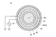
- FIG. 2 shows the arrangement of the members in the chamber 20 when viewed along the central axis of the chamber 20. In FIG. 2, each member is hatched in consideration of easy viewing.
- the RF electrode 50 extends circumferentially along the inner wall surface of the chamber 20.
- the RF electrode 50 is interrupted at the position on the left side of FIG.
- One end of the RF electrode 50 is connected to a high frequency power source 52.
- the other end of the RF electrode 50 is connected to ground.
- a high frequency voltage is applied to the RF electrode 50 by the high frequency power source 52, a magnetic field that vibrates in the vertical direction is generated in the space 54 surrounded by the RF electrode 50 in FIG.
- an oscillating magnetic field is generated in the space 54, plasma is generated in the space 54 as described later.
- the space 54 is referred to as a plasma generation space 54.
- the center electrode 42 is installed below the plasma generation space 54.
- the central electrode 42 is installed at a position through which a central axis 32a of a mounting surface 32 of the stage 30 described later passes.
- the center electrode 42 has a disk shape centered on the central axis 32a.
- the diameter of the central electrode 42 is smaller than the inner diameter of the RF electrode 50.
- the center electrode 42 is connected to ground.
- the outer peripheral electrode 40 is installed below the central electrode 42.
- the outer peripheral electrode 40 has a cylindrical shape extending in the vertical direction in the chamber 20.
- the central axis of the outer peripheral electrode 40 substantially coincides with the central axis 32a.
- the inner diameter of the outer peripheral electrode 40 is larger than the diameter of the central electrode 42. That is, as shown in FIG. 2, the outer peripheral electrode 40 extends along the outer periphery of the central electrode 42 with a distance from the central electrode 42 when viewed along the central axis 32 a.
- the outer peripheral electrode 40 is connected to the ground.
- the stage 30 is installed at the bottom of the chamber 20.
- a mounting surface 32 is formed on the upper surface of the stage 30.
- the mounting surface 32 is a flat surface, and its outer shape is circular.
- a wafer 34 that is a workpiece can be placed on the placement surface 32.
- the center axis 32 a of the mounting surface 32 substantially coincides with the center axis of the inner wall surface of the chamber 20.
- the diameter of the stage 30 is smaller than the inner diameter of the outer peripheral electrode 40. That is, the diameter of the mounting surface 32 is smaller than the inner diameter of the outer peripheral electrode 40.
- the stage 30 is a conductor.
- the stage 30 is connected to the ground via a blocking capacitor 36.
- the wafer 34 is placed on the placement surface 32 of the stage 30.
- an exhaust pump (not shown) is operated to exhaust the gas in the chamber 20 from the exhaust pipe 38.
- the atmospheric pressure in the chamber 20 is lowered.
- the etching gas is supplied through the etching gas supply pipe 62 while the exhaust pump is continuously operated.
- the etching gas flows into the chamber 20 through the vent holes of the shower plate 60.
- a high frequency voltage is applied to the RF electrode 50 by the high frequency power source 52.
- an oscillating magnetic field is generated in the plasma generation space 54.
- the etching gas in the plasma generation space 54 is ionized by the generated oscillating magnetic field.
- plasma is generated in the plasma generation space 54.
- the etching gas SF 6 is decomposed to generate radicals (F * , SF 5 * , SF 4 * ), ions (SF 5 + , SF 4 2+ ), and electrons.
- the electrons are generated, they are instantaneously drawn into the shower plate 60 and the stage 30. Therefore, plasma composed of radicals and ions is generated in the plasma generation space 54.
- plasma continues to be generated in the plasma generation space 54.
- a higher magnetic field is generated in a region on the outer peripheral side closer to the RF electrode 50 than in a central region (that is, a region in the vicinity of the central axis 32a) far from the RF electrode 50. For this reason, in the region on the outer peripheral side of the plasma generation space 54, a plasma having a higher concentration than that in the central region of the plasma generation space 54 is generated.
- Plasma generated in the plasma generation space 54 flows downward in the chamber 20 due to the repulsive force between ions and the flow of gas in the chamber 20. That is, plasma flows from the plasma generation space 54 through the space between the central electrode 42 and the outer peripheral electrode 40 into the space 44 on the stage 30. As described above, the stage 30 is negatively charged. That is, the stage 30 having a negative potential exists below the space 44. On the other hand, since the center electrode 42 and the outer peripheral electrode 40 are connected to the ground, their potential is 0V. That is, the space 44 is surrounded by the center electrode 42 and the outer peripheral electrode 40 having a potential of 0 V on the upper side and the side. Therefore, the potential is distributed in the space 44 as represented by the equipotential line 100 in FIG.
- the potential is distributed so that the equipotential line 100 protrudes upward at a position close to the central axis 32a.
- an electric field is generated in the space 44 from the outer peripheral electrode 40 side toward the central axis 32a side.
- the ions move in a direction substantially orthogonal to the equipotential line 100. Accordingly, as indicated by an arrow 110 in FIG. 3, the ions move downward while moving toward the central axis 32a.
- plasma that is, ions
- plasma that is, ions
- the concentration of ions becomes uniform as the wafer 34 is approached.
- the ion concentration distribution is more uniform near the surface of the wafer 34. For this reason, the number of ions colliding with the surface of the wafer 34 becomes more uniform within the surface.
- the reaction between the radical and the wafer 34 is promoted by the collision of ions with the wafer 34. For this reason, the reaction between radicals and the wafer 34 is also made uniform within the surface of the wafer 34. Therefore, according to the etching apparatus 10, the surface of the wafer 34 can be uniformly etched.
- FIG. 4 shows the processing amount when the etching apparatus 10 etches the wafer for a certain time.
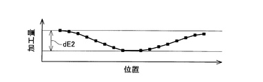
- FIG. 5 shows the processing amount when the wafer is etched for the same time as the etching in FIG. 4 by an etching apparatus that does not have the center electrode 42 and the outer peripheral electrode 40.
- the SiO 2 film was etched in order to accurately grasp the ion concentration distribution. Since the SiO 2 film hardly reacts with radicals, the amount of processing in FIGS. 4 and 5 is dominated by the amount of processing by ion collision. 4 and 5, the horizontal axis indicates the position of the wafer in the radial direction. In FIG.
- the average processing amount of the whole wafer is about 67 ⁇ m, whereas the processing amount difference dE1 between the central portion of the wafer and the outer peripheral portion of the wafer is about 2.5 ⁇ m.
- the ratio of the difference dE1 to the average processing amount is about 3.7%.
- the average processing amount of the entire wafer is about 54 ⁇ m, whereas the processing amount difference dE2 between the central portion of the wafer and the outer peripheral portion of the wafer is about 4.5 ⁇ m.
- the ratio of the difference dE2 to the average processing amount is about 8.3%.
- the central electrode 42 and the outer peripheral electrode 40 can generate an electric field toward the center of the mounting surface 32 in the space 44 on the stage 30. For this reason, the etching apparatus 10 can etch the wafer 34 uniformly. It is also possible to generate an electric field toward the center of the mounting surface 32 only by the outer peripheral electrode 40 without installing the central electrode 42. However, in this case, the potential distribution in the space 44 on the stage 30 varies according to the unstable potential in the plasma generation space 54. For this reason, it is difficult to etch the wafer 30 uniformly unless the central electrode 42 exists.
- the etching apparatus 10 of the present embodiment since the central electrode 42 is present, the potential distribution of the space 44 on the stage 30 can be controlled without being substantially affected by the potential of the plasma generation space 54. Therefore, the etching apparatus 10 can etch the wafer 30 uniformly.
- the etching apparatus 10 makes the concentration distribution of ions uniform on the surface of the wafer 34 by moving the high concentration ions generated in the outer peripheral portion of the plasma generation space 54 toward the central axis 32 a of the wafer 34. For this reason, most of the generated ions contribute to the etching of the wafer 34. Therefore, this etching apparatus 10 can perform etching efficiently.
- the center electrode 42 and the outer peripheral electrode 40 are connected to the ground.
- the central electrode 42 and the outer peripheral electrode 40 may be controlled to a constant potential by the DC power sources 90 and 92.
- the central electrode 42 and the outer peripheral electrode 40 are controlled to a potential lower than the potential of the plasma generation space 54 and higher than the potential of the stage 30, thereby making it possible to make the ion concentration distribution uniform on the wafer surface. it can.
- the applied voltage of the DC power supplies 90 and 92 can be changed.
- the applied voltage of the DC power supply 90 may be linked to the applied voltage of the DC power supply 92.
- the applied voltage of the DC power supply 90 can be controlled independently of the applied voltage of the DC power supply 92. It is preferable to keep it. According to such a configuration, the potential distribution in the space 44 on the stage 30 can be controlled more finely.
- a single electrode 98 may be installed between the plasma generation space 54 and the stage 30.
- the electrode 98 is formed with a large number of air holes communicating from the upper surface thereof to the lower surface thereof.
- the plasma generated in the plasma generation space 54 flows to the wafer 34 side through the vent hole of the electrode 98.
- the electrode 98 has a central portion 98a located on the central axis 32a and an outer peripheral portion 98b located below the central portion 98a and extending along the periphery of the central portion 98a.
- the central portion 98a functions in the same manner as the central electrode 42 described above.
- the outer peripheral portion 98b functions in the same manner as the outer peripheral electrode 40 described above.
- the potential distribution in the space 44 can also be controlled by the electrode 98 as in FIG. Since the center part 98a and the outer peripheral part 98b are connected, the electrode 98 can be formed in a more complicated shape. For this reason, the potential distribution in the space 44 can be controlled more appropriately.
- etching apparatus 210 Refers to the second embodiment shown in FIG. 8
- the chamber 220, stage 230, outer peripheral electrode 240, center electrode 242 and the like of the etching apparatus 210 of the second embodiment are configured in the same manner as the etching apparatus 10 of the first embodiment.
- a coil 270 and a coil 272 are installed above the chamber 220.
- the coil 270 is disposed inside the coil 272.
- the coils 270 and 272 are arranged concentrically with the central axis 232 a of the mounting surface 232 of the stage 230. Both ends of the winding of the coil 270 are connected to a high frequency power supply 256.
- Both ends of the winding of the coil 272 are connected to a high frequency power source 258.
- the coil 270 and the coil 272 are arranged at a distance, and a plasma generation space 254 is formed between them.
- An etching gas supply pipe 262 is connected to a position connected to the plasma generation space 254 on the upper surface of the chamber 220.
- the etching gas is supplied from the etching gas supply pipe 262 into the plasma generation space 254 after the inside of the chamber 220 is depressurized. Then, a high frequency voltage is applied to the coils 270 and 272. As a result, an oscillating magnetic field is generated in the plasma generation space 254, and plasma is generated in the plasma generation space 254. Note that plasma is not generated in a region inside the winding of the coil 270 (that is, a region through which the central axis 232a of the mounting surface 232 passes). The plasma generated in the plasma generation space 254 etches the wafer 234 in the same manner as the etching apparatus 210 of the first embodiment.
- the ion concentration distribution on the surface of the wafer 234 is made uniform by the electric field formed by the central electrode 242 and the outer peripheral electrode 240. Therefore, according to the etching apparatus 210, the wafer 234 can be uniformly etched.
Landscapes
- Physics & Mathematics (AREA)
- Engineering & Computer Science (AREA)
- Plasma & Fusion (AREA)
- Chemical & Material Sciences (AREA)
- Analytical Chemistry (AREA)
- Drying Of Semiconductors (AREA)
- Plasma Technology (AREA)
Abstract
Description
第1実施例に係るエッチング装置について説明する。図1に示すように、エッチング装置10は、チャンバ20を備えている。チャンバ20の上部には、エッチングガス供給管62が接続されている。エッチングガス供給管62は、チャンバ20内にエッチングガス(本実施例では、SF6)を供給する。また、チャンバ20の下部には、排気管38が接続されている。排気管38は、図示しない排気ポンプに接続されている。排気管38は、図1の矢印80に示すように、チャンバ20内のガスを排気する。チャンバ20内には、シャワープレート60、RF電極50、中央電極42、外周電極40、及び、ステージ30が設置されている。
次に、図8に示す第2実施例のエッチング装置210について説明する。第2実施例のエッチング装置210のチャンバ220、ステージ230、外周電極240、中央電極242等は、第1実施例のエッチング装置10と同様に構成されている。エッチング装置210では、チャンバ220の上部に、コイル270とコイル272が設置されている。コイル270は、コイル272の内側に配置されている。コイル270、272は、ステージ230の載置面232の中心軸232aと同心状に配置されている。コイル270の巻き線の両端は、高周波電源256に接続されている。コイル272の巻き線の両端は、高周波電源258に接続されている。コイル270とコイル272は距離を隔てて配置されており、これらの間にプラズマ発生空間254が形成されている。チャンバ220の上面のプラズマ発生空間254に繋がる位置には、エッチングガス供給管262が接続されている。
Claims (5)
- プラズマを用いて被加工物をエッチングするエッチング装置であって、
載置面を有しており、載置面に被加工物が載置されるステージと、
ステージの上方において、載置面の中心軸上よりも、その中心軸の周囲の空間で高濃度にプラズマを発生させるプラズマ発生手段と、
プラズマ発生手段がプラズマを発生させる空間よりも下側に設置されており、前記中心軸が通過する位置に設置されており、電位を制御可能な中央電極と、
ステージよりも上側、かつ、中央電極よりも下側に設置されており、前記中心軸に沿って見たときに、中央電極の周囲に沿って伸びており、電位を制御可能な外周電極、
を備えていることを特徴とするエッチング装置。 - 外周電極が、上下方向に伸びていることを特徴とする請求項1に記載のエッチング装置。
- 中央電極の電位及び外周電極の電位を、プラズマ発生手段がプラズマを発生させる空間の電位より低く、ステージの電位より高い電位に制御する電位制御手段をさらに有していることを特徴とする請求項1または2に記載のエッチング装置。
- 電位制御手段が、中央電極の電位と、外周電極の電位とを独立して変更可能であることを特徴とする請求項3に記載のエッチング装置。
- 中央電極と外周電極が、これらを互いに連結した1つの電極により構成されており、
その電極に、上面と下面とを連通する複数の通気孔が形成されている、
ことを特徴とする請求項1~3の何れか一項に記載のエッチング装置。
Priority Applications (5)
| Application Number | Priority Date | Filing Date | Title |
|---|---|---|---|
| CN201080019940.5A CN102439701B (zh) | 2010-07-21 | 2010-07-21 | 蚀刻装置 |
| DE112010003657.8T DE112010003657B4 (de) | 2010-07-21 | 2010-07-21 | Ätzanlage |
| PCT/JP2010/062267 WO2012011171A1 (ja) | 2010-07-21 | 2010-07-21 | エッチング装置 |
| JP2011529796A JP5382125B2 (ja) | 2010-07-21 | 2010-07-21 | エッチング装置 |
| US13/275,985 US20130020027A1 (en) | 2010-07-21 | 2011-10-18 | Etching equipment |
Applications Claiming Priority (1)
| Application Number | Priority Date | Filing Date | Title |
|---|---|---|---|
| PCT/JP2010/062267 WO2012011171A1 (ja) | 2010-07-21 | 2010-07-21 | エッチング装置 |
Related Child Applications (1)
| Application Number | Title | Priority Date | Filing Date |
|---|---|---|---|
| US13/275,985 Continuation US20130020027A1 (en) | 2010-07-21 | 2011-10-18 | Etching equipment |
Publications (1)
| Publication Number | Publication Date |
|---|---|
| WO2012011171A1 true WO2012011171A1 (ja) | 2012-01-26 |
Family
ID=45496611
Family Applications (1)
| Application Number | Title | Priority Date | Filing Date |
|---|---|---|---|
| PCT/JP2010/062267 Ceased WO2012011171A1 (ja) | 2010-07-21 | 2010-07-21 | エッチング装置 |
Country Status (5)
| Country | Link |
|---|---|
| US (1) | US20130020027A1 (ja) |
| JP (1) | JP5382125B2 (ja) |
| CN (1) | CN102439701B (ja) |
| DE (1) | DE112010003657B4 (ja) |
| WO (1) | WO2012011171A1 (ja) |
Cited By (1)
| Publication number | Priority date | Publication date | Assignee | Title |
|---|---|---|---|---|
| JP2017033788A (ja) * | 2015-08-03 | 2017-02-09 | 日新電機株式会社 | プラズマ処理装置 |
Families Citing this family (5)
| Publication number | Priority date | Publication date | Assignee | Title |
|---|---|---|---|---|
| CN106415779B (zh) * | 2013-12-17 | 2020-01-21 | 东京毅力科创株式会社 | 用于控制等离子体密度的系统和方法 |
| JP6305087B2 (ja) * | 2014-02-07 | 2018-04-04 | 株式会社日立ハイテクノロジーズ | プラズマ処理方法 |
| US9514918B2 (en) * | 2014-09-30 | 2016-12-06 | Applied Materials, Inc. | Guard aperture to control ion angular distribution in plasma processing |
| EP3309815B1 (de) * | 2016-10-12 | 2019-03-20 | Meyer Burger (Germany) AG | Plasmabehandlungsvorrichtung mit zwei, miteinander gekoppelten mikrowellenplasmaquellen sowie verfahren zum betreiben einer solchen plasmabehandlungsvorrichtung |
| KR102923846B1 (ko) | 2021-10-18 | 2026-02-04 | 삼성전자주식회사 | 플라즈마 식각 장치 및 이의 동작 방법 |
Citations (3)
| Publication number | Priority date | Publication date | Assignee | Title |
|---|---|---|---|---|
| JPS5676242A (en) * | 1979-11-26 | 1981-06-23 | Tokyo Ohka Kogyo Co Ltd | Treating apparatus using gas plasma reaction |
| JPH01238120A (ja) * | 1988-03-18 | 1989-09-22 | Fujitsu Ltd | エッチング装置 |
| JPH06252097A (ja) * | 1993-02-25 | 1994-09-09 | Hitachi Ltd | プラズマエッチング装置 |
Family Cites Families (5)
| Publication number | Priority date | Publication date | Assignee | Title |
|---|---|---|---|---|
| JPH09293706A (ja) * | 1996-04-25 | 1997-11-11 | Nec Kagoshima Ltd | ドライエッチング装置 |
| US6203657B1 (en) * | 1998-03-31 | 2001-03-20 | Lam Research Corporation | Inductively coupled plasma downstream strip module |
| US6706142B2 (en) | 2000-11-30 | 2004-03-16 | Mattson Technology, Inc. | Systems and methods for enhancing plasma processing of a semiconductor substrate |
| JP2002289585A (ja) * | 2001-03-26 | 2002-10-04 | Ebara Corp | 中性粒子ビーム処理装置 |
| JP4456412B2 (ja) | 2004-05-27 | 2010-04-28 | 株式会社日立製作所 | プラズマ処理装置 |
-
2010
- 2010-07-21 WO PCT/JP2010/062267 patent/WO2012011171A1/ja not_active Ceased
- 2010-07-21 CN CN201080019940.5A patent/CN102439701B/zh not_active Expired - Fee Related
- 2010-07-21 JP JP2011529796A patent/JP5382125B2/ja not_active Expired - Fee Related
- 2010-07-21 DE DE112010003657.8T patent/DE112010003657B4/de not_active Expired - Fee Related
-
2011
- 2011-10-18 US US13/275,985 patent/US20130020027A1/en not_active Abandoned
Patent Citations (3)
| Publication number | Priority date | Publication date | Assignee | Title |
|---|---|---|---|---|
| JPS5676242A (en) * | 1979-11-26 | 1981-06-23 | Tokyo Ohka Kogyo Co Ltd | Treating apparatus using gas plasma reaction |
| JPH01238120A (ja) * | 1988-03-18 | 1989-09-22 | Fujitsu Ltd | エッチング装置 |
| JPH06252097A (ja) * | 1993-02-25 | 1994-09-09 | Hitachi Ltd | プラズマエッチング装置 |
Cited By (1)
| Publication number | Priority date | Publication date | Assignee | Title |
|---|---|---|---|---|
| JP2017033788A (ja) * | 2015-08-03 | 2017-02-09 | 日新電機株式会社 | プラズマ処理装置 |
Also Published As
| Publication number | Publication date |
|---|---|
| CN102439701B (zh) | 2014-07-09 |
| CN102439701A (zh) | 2012-05-02 |
| JP5382125B2 (ja) | 2014-01-08 |
| US20130020027A1 (en) | 2013-01-24 |
| DE112010003657T5 (de) | 2013-03-28 |
| DE112010003657B4 (de) | 2014-08-21 |
| JPWO2012011171A1 (ja) | 2013-09-09 |
Similar Documents
| Publication | Publication Date | Title |
|---|---|---|
| KR102453450B1 (ko) | 플라즈마 처리 장치, 반도체 소자의 제조설비 및 그의 제조방법 | |
| CN107636793B (zh) | 离子对离子等离子体原子层蚀刻工艺及反应器 | |
| TWI645443B (zh) | 電漿處理裝置及電漿處理方法 | |
| CN105097403B (zh) | 等离子体处理装置 | |
| JP6008771B2 (ja) | 多層膜をエッチングする方法 | |
| KR20210038938A (ko) | 플라즈마 공정을 위한 방법 및 장치 | |
| JP5382125B2 (ja) | エッチング装置 | |
| JP7262375B2 (ja) | プラズマ処理方法及びプラズマ処理装置 | |
| US11043387B2 (en) | Methods and apparatus for processing a substrate | |
| CN112466734B (zh) | 等离子体处理装置及处理基板的方法 | |
| US20170186591A1 (en) | Cleaning method of plasma processing apparatus and plasma processing apparatus | |
| WO2011102083A1 (ja) | プラズマ処理装置及びプラズマ処理方法 | |
| CN111146061B (zh) | 等离子体处理装置和等离子体处理方法 | |
| CN109767967B (zh) | 基板处理方法和基板处理装置 | |
| TW201711529A (zh) | 基底處理設備 | |
| US20200006036A1 (en) | Methods and apparatus for electron beam etching process | |
| CN115398594B (zh) | 用于远程等离子体工艺的对称中空阴极电极和放电模式的方法和设备 | |
| JP2012164766A (ja) | エッチング装置 | |
| WO2018173227A1 (ja) | 中性粒子ビーム処理装置 | |
| JP2007134428A (ja) | ドライエッチング方法およびその装置 | |
| KR20080060834A (ko) | 플라즈마 처리 장치 | |
| JPH07153741A (ja) | プラズマ処理システム | |
| JP2002305183A (ja) | ビーム処理装置 | |
| KR20090043863A (ko) | 플라즈마 기판 처리 장치 |
Legal Events
| Date | Code | Title | Description |
|---|---|---|---|
| WWE | Wipo information: entry into national phase |
Ref document number: 201080019940.5 Country of ref document: CN |
|
| WWE | Wipo information: entry into national phase |
Ref document number: 2011529796 Country of ref document: JP |
|
| 121 | Ep: the epo has been informed by wipo that ep was designated in this application |
Ref document number: 10855008 Country of ref document: EP Kind code of ref document: A1 |
|
| WWE | Wipo information: entry into national phase |
Ref document number: 1120100036578 Country of ref document: DE Ref document number: 112010003657 Country of ref document: DE |
|
| 122 | Ep: pct application non-entry in european phase |
Ref document number: 10855008 Country of ref document: EP Kind code of ref document: A1 |