WO2012008343A1 - インプリントモールド用TiO2含有石英ガラス基材およびその製造方法 - Google Patents
インプリントモールド用TiO2含有石英ガラス基材およびその製造方法 Download PDFInfo
- Publication number
- WO2012008343A1 WO2012008343A1 PCT/JP2011/065497 JP2011065497W WO2012008343A1 WO 2012008343 A1 WO2012008343 A1 WO 2012008343A1 JP 2011065497 W JP2011065497 W JP 2011065497W WO 2012008343 A1 WO2012008343 A1 WO 2012008343A1
- Authority
- WO
- WIPO (PCT)
- Prior art keywords
- tio
- glass substrate
- quartz glass
- containing quartz
- less
- Prior art date
- Legal status (The legal status is an assumption and is not a legal conclusion. Google has not performed a legal analysis and makes no representation as to the accuracy of the status listed.)
- Ceased
Links
Images

Classifications
-
- C—CHEMISTRY; METALLURGY
- C03—GLASS; MINERAL OR SLAG WOOL
- C03B—MANUFACTURE, SHAPING, OR SUPPLEMENTARY PROCESSES
- C03B19/00—Other methods of shaping glass
- C03B19/14—Other methods of shaping glass by gas- or vapour- phase reaction processes
-
- B—PERFORMING OPERATIONS; TRANSPORTING
- B29—WORKING OF PLASTICS; WORKING OF SUBSTANCES IN A PLASTIC STATE IN GENERAL
- B29D—PRODUCING PARTICULAR ARTICLES FROM PLASTICS OR FROM SUBSTANCES IN A PLASTIC STATE
- B29D11/00—Producing optical elements, e.g. lenses or prisms
- B29D11/0074—Production of other optical elements not provided for in B29D11/00009- B29D11/0073
- B29D11/00769—Producing diffraction gratings
-
- B—PERFORMING OPERATIONS; TRANSPORTING
- B29—WORKING OF PLASTICS; WORKING OF SUBSTANCES IN A PLASTIC STATE IN GENERAL
- B29C—SHAPING OR JOINING OF PLASTICS; SHAPING OF MATERIAL IN A PLASTIC STATE, NOT OTHERWISE PROVIDED FOR; AFTER-TREATMENT OF THE SHAPED PRODUCTS, e.g. REPAIRING
- B29C33/00—Moulds or cores; Details thereof or accessories therefor
- B29C33/38—Moulds or cores; Details thereof or accessories therefor characterised by the material or the manufacturing process
-
- B—PERFORMING OPERATIONS; TRANSPORTING
- B24—GRINDING; POLISHING
- B24B—MACHINES, DEVICES, OR PROCESSES FOR GRINDING OR POLISHING; DRESSING OR CONDITIONING OF ABRADING SURFACES; FEEDING OF GRINDING, POLISHING, OR LAPPING AGENTS
- B24B9/00—Machines or devices designed for grinding edges or bevels on work or for removing burrs; Accessories therefor
- B24B9/02—Machines or devices designed for grinding edges or bevels on work or for removing burrs; Accessories therefor characterised by a special design with respect to properties of materials specific to articles to be ground
- B24B9/06—Machines or devices designed for grinding edges or bevels on work or for removing burrs; Accessories therefor characterised by a special design with respect to properties of materials specific to articles to be ground of non-metallic inorganic material, e.g. stone, ceramics, porcelain
- B24B9/08—Machines or devices designed for grinding edges or bevels on work or for removing burrs; Accessories therefor characterised by a special design with respect to properties of materials specific to articles to be ground of non-metallic inorganic material, e.g. stone, ceramics, porcelain of glass
- B24B9/10—Machines or devices designed for grinding edges or bevels on work or for removing burrs; Accessories therefor characterised by a special design with respect to properties of materials specific to articles to be ground of non-metallic inorganic material, e.g. stone, ceramics, porcelain of glass of plate glass
-
- B—PERFORMING OPERATIONS; TRANSPORTING
- B29—WORKING OF PLASTICS; WORKING OF SUBSTANCES IN A PLASTIC STATE IN GENERAL
- B29C—SHAPING OR JOINING OF PLASTICS; SHAPING OF MATERIAL IN A PLASTIC STATE, NOT OTHERWISE PROVIDED FOR; AFTER-TREATMENT OF THE SHAPED PRODUCTS, e.g. REPAIRING
- B29C59/00—Surface shaping of articles, e.g. embossing; Apparatus therefor
- B29C59/002—Component parts, details or accessories; Auxiliary operations
-
- B—PERFORMING OPERATIONS; TRANSPORTING
- B29—WORKING OF PLASTICS; WORKING OF SUBSTANCES IN A PLASTIC STATE IN GENERAL
- B29C—SHAPING OR JOINING OF PLASTICS; SHAPING OF MATERIAL IN A PLASTIC STATE, NOT OTHERWISE PROVIDED FOR; AFTER-TREATMENT OF THE SHAPED PRODUCTS, e.g. REPAIRING
- B29C59/00—Surface shaping of articles, e.g. embossing; Apparatus therefor
- B29C59/02—Surface shaping of articles, e.g. embossing; Apparatus therefor by mechanical means, e.g. pressing
- B29C59/026—Surface shaping of articles, e.g. embossing; Apparatus therefor by mechanical means, e.g. pressing of layered or coated substantially flat surfaces
-
- C—CHEMISTRY; METALLURGY
- C03—GLASS; MINERAL OR SLAG WOOL
- C03B—MANUFACTURE, SHAPING, OR SUPPLEMENTARY PROCESSES
- C03B19/00—Other methods of shaping glass
- C03B19/14—Other methods of shaping glass by gas- or vapour- phase reaction processes
- C03B19/1453—Thermal after-treatment of the shaped article, e.g. dehydrating, consolidating, sintering
-
- C—CHEMISTRY; METALLURGY
- C03—GLASS; MINERAL OR SLAG WOOL
- C03C—CHEMICAL COMPOSITION OF GLASSES, GLAZES OR VITREOUS ENAMELS; SURFACE TREATMENT OF GLASS; SURFACE TREATMENT OF FIBRES OR FILAMENTS MADE FROM GLASS, MINERALS OR SLAGS; JOINING GLASS TO GLASS OR OTHER MATERIALS
- C03C19/00—Surface treatment of glass, not in the form of fibres or filaments, by mechanical means
-
- C—CHEMISTRY; METALLURGY
- C03—GLASS; MINERAL OR SLAG WOOL
- C03C—CHEMICAL COMPOSITION OF GLASSES, GLAZES OR VITREOUS ENAMELS; SURFACE TREATMENT OF GLASS; SURFACE TREATMENT OF FIBRES OR FILAMENTS MADE FROM GLASS, MINERALS OR SLAGS; JOINING GLASS TO GLASS OR OTHER MATERIALS
- C03C3/00—Glass compositions
- C03C3/04—Glass compositions containing silica
- C03C3/06—Glass compositions containing silica with more than 90% silica by weight, e.g. quartz
-
- G—PHYSICS
- G03—PHOTOGRAPHY; CINEMATOGRAPHY; ANALOGOUS TECHNIQUES USING WAVES OTHER THAN OPTICAL WAVES; ELECTROGRAPHY; HOLOGRAPHY
- G03F—PHOTOMECHANICAL PRODUCTION OF TEXTURED OR PATTERNED SURFACES, e.g. FOR PRINTING, FOR PROCESSING OF SEMICONDUCTOR DEVICES; MATERIALS THEREFOR; ORIGINALS THEREFOR; APPARATUS SPECIALLY ADAPTED THEREFOR
- G03F7/00—Photomechanical, e.g. photolithographic, production of textured or patterned surfaces, e.g. printing surfaces; Materials therefor, e.g. comprising photoresists; Apparatus specially adapted therefor
- G03F7/0002—Lithographic processes using patterning methods other than those involving the exposure to radiation, e.g. by stamping
-
- C—CHEMISTRY; METALLURGY
- C03—GLASS; MINERAL OR SLAG WOOL
- C03B—MANUFACTURE, SHAPING, OR SUPPLEMENTARY PROCESSES
- C03B2201/00—Type of glass produced
- C03B2201/06—Doped silica-based glasses
- C03B2201/07—Impurity concentration specified
- C03B2201/075—Hydroxyl ion (OH)
-
- C—CHEMISTRY; METALLURGY
- C03—GLASS; MINERAL OR SLAG WOOL
- C03B—MANUFACTURE, SHAPING, OR SUPPLEMENTARY PROCESSES
- C03B2201/00—Type of glass produced
- C03B2201/06—Doped silica-based glasses
- C03B2201/30—Doped silica-based glasses doped with metals, e.g. Ga, Sn, Sb, Pb or Bi
- C03B2201/40—Doped silica-based glasses doped with metals, e.g. Ga, Sn, Sb, Pb or Bi doped with transition metals other than rare earth metals, e.g. Zr, Nb, Ta or Zn
- C03B2201/42—Doped silica-based glasses doped with metals, e.g. Ga, Sn, Sb, Pb or Bi doped with transition metals other than rare earth metals, e.g. Zr, Nb, Ta or Zn doped with titanium
-
- C—CHEMISTRY; METALLURGY
- C03—GLASS; MINERAL OR SLAG WOOL
- C03C—CHEMICAL COMPOSITION OF GLASSES, GLAZES OR VITREOUS ENAMELS; SURFACE TREATMENT OF GLASS; SURFACE TREATMENT OF FIBRES OR FILAMENTS MADE FROM GLASS, MINERALS OR SLAGS; JOINING GLASS TO GLASS OR OTHER MATERIALS
- C03C2201/00—Glass compositions
- C03C2201/06—Doped silica-based glasses
- C03C2201/30—Doped silica-based glasses containing metals
- C03C2201/40—Doped silica-based glasses containing metals containing transition metals other than rare earth metals, e.g. Zr, Nb, Ta or Zn
- C03C2201/42—Doped silica-based glasses containing metals containing transition metals other than rare earth metals, e.g. Zr, Nb, Ta or Zn containing titanium
-
- C—CHEMISTRY; METALLURGY
- C03—GLASS; MINERAL OR SLAG WOOL
- C03C—CHEMICAL COMPOSITION OF GLASSES, GLAZES OR VITREOUS ENAMELS; SURFACE TREATMENT OF GLASS; SURFACE TREATMENT OF FIBRES OR FILAMENTS MADE FROM GLASS, MINERALS OR SLAGS; JOINING GLASS TO GLASS OR OTHER MATERIALS
- C03C2204/00—Glasses, glazes or enamels with special properties
- C03C2204/08—Glass having a rough surface
-
- Y—GENERAL TAGGING OF NEW TECHNOLOGICAL DEVELOPMENTS; GENERAL TAGGING OF CROSS-SECTIONAL TECHNOLOGIES SPANNING OVER SEVERAL SECTIONS OF THE IPC; TECHNICAL SUBJECTS COVERED BY FORMER USPC CROSS-REFERENCE ART COLLECTIONS [XRACs] AND DIGESTS
- Y10—TECHNICAL SUBJECTS COVERED BY FORMER USPC
- Y10T—TECHNICAL SUBJECTS COVERED BY FORMER US CLASSIFICATION
- Y10T428/00—Stock material or miscellaneous articles
- Y10T428/24—Structurally defined web or sheet [e.g., overall dimension, etc.]
- Y10T428/24355—Continuous and nonuniform or irregular surface on layer or component [e.g., roofing, etc.]
Definitions
- the present invention relates to a TiO 2 -containing quartz glass substrate for imprint molds and a method for producing the same.
- an imprint mold having an inverted pattern (transfer pattern) on the surface is pressed against the layer of the photocurable resin formed on the surface of the substrate, and the photocurable resin is applied.
- An optical imprint method that forms a concavo-convex pattern on the surface of a substrate by curing is drawing attention.
- An imprint mold used in the optical imprint method is required to have light transmittance, chemical resistance, and dimensional stability against a temperature rise caused by light irradiation.
- quartz glass is often used from the viewpoint of light transmittance and chemical resistance.
- quartz glass has a high coefficient of thermal expansion around room temperature of about 500 ppb / ° C. and lacks dimensional stability. Therefore, TiO 2 -containing quartz glass has been proposed as a quartz glass having a low thermal expansion coefficient (Patent Documents 1 and 2).
- the TiO 2 -containing quartz glass has a streak (non-uniform composition (composition distribution)), the surface of the TiO 2 -containing quartz glass substrate that is the substrate for imprint molding, particularly the roughness of the side surface, It is difficult to reduce the swell by polishing. And it became clear by the inventors' investigation that the following problems occur when the roughness and waviness of the side surface of the TiO 2 -containing quartz glass substrate are large.
- the present inventors have focused on the stress generated by the strie in the TiO 2 -containing quartz glass substrate, and have reached the present invention.
- the present invention relates to a TiO 2 -containing quartz glass substrate for imprint molds and a method for producing the same, which can suppress defects and misalignment of the concavo-convex pattern transferred to the surface of the substrate by the imprint method when used as an imprint mold. provide.
- Imprint mold TiO 2 -containing quartz glass substrate of the present invention includes a main surface and a side surface, a TiO 2 -containing quartz glass substrate for imprint mold, the arithmetic average roughness of the side surface (Ra) is The root mean square (MSFR_rms) of the irregularities in the wavelength region of 10 ⁇ m to 1 mm on the side surface is 10 nm or less.
- the TiO 2 -containing quartz glass substrate for imprint molds of the present invention preferably has a chamfered surface interposed between the main surface and the side surface for the purpose of preventing chipping and chipping of the outer periphery, and the chamfered surface.
- the arithmetic average roughness (Ra) is preferably 1 nm or less.
- the TiO 2 concentration in the TiO 2 -containing quartz glass substrate for imprint molds of the present invention is preferably 3 to 12% by mass,
- the standard deviation (dev [ ⁇ ]) of stress generated by the strie is 0.05 MPa or less.
- the difference ( ⁇ ) between the maximum value and the minimum value of the stress caused by the stripe is preferably 0.23 MPa or less.
- Manufacturing method of one embodiment according to the imprint mold TiO 2 -containing quartz glass substrate of the present invention includes a main surface and a side surface, a method for producing a TiO imprint mold 2 -containing quartz glass substrate, By polishing the side surface of the TiO 2 -containing quartz glass substrate having a standard deviation (dev [ ⁇ ]) of stress caused by the strie of 0.05 MPa or less, the arithmetic average roughness (Ra) of the side surface is set to 1 nm or less, The root mean square (MSFR_rms) of the irregularities in the wavelength region of 10 ⁇ m to 1 mm on the side surface is set to 10 nm or less.
- the method for producing a TiO 2 -containing quartz glass substrate for imprint molds is a method for producing a TiO 2 -containing quartz glass substrate for imprint molds having a main surface and side surfaces,
- the arithmetic average roughness (Ra) of the side surface is 1 nm or less by polishing the side surface of the TiO 2 -containing quartz glass substrate having a difference ( ⁇ ) between the maximum value and the minimum value of the stress generated by the striee of 0.23 MPa or less.
- the root mean square (MSFR_rms) of the irregularities in the wavelength region of 10 ⁇ m to 1 mm on the side surface is set to 10 nm or less.
- a polishing brush having polishing bristles protruding while supplying a polishing liquid containing abrasive grains and the TiO 2 -containing quartz It is preferable that the side surface of the TiO 2 -containing quartz glass substrate is polished by relatively moving the glass substrate.
- TiO 2 -containing quartz glass substrate for imprint molds of the present invention
- TiO 2 -containing quartz glass substrate has a chamfered surface interposed between the main surface and the side surface
- the arithmetic average roughness (Ra) of the chamfered surface is preferably 1 nm or less by polishing the chamfered surface together with the side surface of the containing quartz glass substrate.
- Imprint mold TiO 2 -containing quartz glass substrate of the present invention when used as an imprint mold, it is possible to suppress the defects and misalignment of the uneven pattern transferred to the surface of the substrate by imprinting.
- the method for producing a TiO 2 -containing quartz glass substrate for imprint molds of the present invention when used as an imprint mold, it is possible to suppress defects and misalignment of the concavo-convex pattern transferred to the surface of the substrate by the imprint method.
- a TiO 2 -containing quartz glass substrate for imprint mold can be produced.
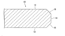
- Figure 1 is a cross-sectional view in the vicinity of the periphery of an example of an imprint mold TiO 2 -containing quartz glass substrate of the present invention.
- FIG. 2 is a cross-sectional view around the periphery showing another example of the TiO 2 -containing quartz glass substrate for imprint molds of the present invention.
- FIG. 1 is a cross-sectional view in the vicinity of the periphery showing an example of a TiO 2 -containing quartz glass substrate for imprint molds of the present invention.
- the imprint mold TiO 2 -containing quartz glass substrate 10 has two main surfaces 12, a side surface 14 formed on the periphery of the imprint mold TiO 2 -containing quartz glass substrate 10, a main surface 12 and a side surface 14. And two chamfered surfaces 16 interposed therebetween.
- the TiO 2 -containing quartz glass substrate 10 for imprint molds preferably has a chamfered surface 16 from the viewpoint of suppressing peripheral chipping and chipping, but does not necessarily have a chamfered surface as shown in FIG. May be.
- the arithmetic average roughness (Ra) of the side surface 14 is 1 nm or less, preferably 0.7 nm or less, and more preferably 0.5 nm or less.
- the arithmetic average roughness (Ra) is 1 nm or less, fine particles such as abrasive grains used for polishing the side surface 14 are difficult to adhere to the side surface 14.
- fine particles can be removed without causing problems on the main surface by performing scrubbing using a PVA sponge on the side surface.
- the arithmetic average roughness (Ra) is the arithmetic average roughness (Ra) defined in JIS B 0601: 2001, and the surface roughness is measured using an atomic force microscope (AFM) for an area of 1 ⁇ m ⁇ 1 ⁇ m. Calculate from the result.
- the root mean square (MSFR_rms) of irregularities in the wavelength region of 10 ⁇ m to 1 mm on the side surface 14 is 10 nm or less, preferably 7 nm or less, and more preferably 5 nm or less.
- the root mean square (MSFR_rms) of the unevenness is an index of the waviness of the side surface 14, and if the root mean square (MSFR_rms) of the unevenness is 10 nm or less, the fine particles such as the abrasive grains used for polishing the side surface 14 are side surfaces. It is possible to remove fine particles without causing a problem on the main surface by performing scrubbing cleaning using a PVA sponge on the side surface. Further, when the imprint mold is used, the positional deviation caused by the waviness of the side surface 14 hardly occurs.
- the root mean square (MSFR_rms) of the unevenness in the wavelength region of 10 ⁇ m to 1 mm on the side surface 14 is preferably 0.1 nm or more, more preferably 0.5 nm or more, and further preferably 1 nm or more. If the root mean square (MSFR_rms) of the unevenness is 0.1 nm or more, the contact area is reduced and charging of the side surface 14 can be suppressed. In addition, adhesion of fine particles to the side surface 14 due to charging can be suppressed.
- the root mean square (MSFR_rms) of the irregularities in the wavelength region of 10 ⁇ m to 1 mm is measured by measuring the surface roughness using a non-contact surface shape measuring device (for example, New View, etc., manufactured by ZYGO) for a region of 2 mm ⁇ 2 mm. It is calculated from the result of applying a band pass filter that becomes a spatial region (10 ⁇ m to 1 mm).
- a non-contact surface shape measuring device for example, New View, etc., manufactured by ZYGO
- the arithmetic average roughness (Ra) of the chamfered surface 16 is preferably 1 nm or less, more preferably 0.7 nm or less, and further preferably 0.5 nm or less.
- the arithmetic average roughness (Ra) is 1 nm or less, fine particles such as abrasive grains used for polishing the chamfered surface 16 are difficult to adhere to the chamfered surface 16.
- fine particles can be removed without causing problems on the main surface by performing scrubbing using a PVA sponge on the side surface.
- TiO 2 concentration in the TiO 2 -containing quartz glass substrate 10 for imprint mold (100 mass%) is preferably 3 to 12 mass%. Since the TiO 2 -containing quartz glass substrate 10 for imprint mold is used as the substrate for imprint mold, dimensional stability with respect to temperature change is required. If TiO 2 concentration of 3 to 12 mass%, it is possible to reduce the thermal expansion coefficient at near room temperature. In order to make the thermal expansion coefficient near room temperature almost zero, the TiO 2 concentration is more preferably 5 to 9% by mass, and further preferably 6 to 8% by mass. The TiO 2 concentration is measured using a fundamental parameter (FP) method in a fluorescent X-ray analysis method.
- FP fundamental parameter
- Ti 3+ concentration The average Ti 3+ concentration in the TiO 2 -containing quartz glass substrate 10 for imprint molds is preferably 100 ppm by mass or less, more preferably 70 ppm by mass or less, further preferably 20 ppm by mass or less, and more preferably 10 ppm by mass or less. Particularly preferred.
- the Ti 3+ concentration affects the coloring of TiO 2 -containing quartz glass for imprint molds, particularly the internal transmittance T 300 to 700 . If the Ti 3+ concentration is 100 mass ppm or less, brown coloring is suppressed, and as a result, a decrease in internal transmittance T 300 to 700 is suppressed, and transparency is improved.
- the Ti 3+ concentration is obtained by electron spin resonance (ESR) measurement.
- ESR electron spin resonance
- the measurement conditions are as follows. Frequency: Near 9.44 GHz (X-band), Output: 4mW Modulating magnetic field: 100 KHz, 0.2 mT, Measurement temperature: room temperature, ESR seed integration range: 332 to 368 mT, Sensitivity calibration: performed at a certain amount of peak height of Mn 2+ / MgO.
- the Ti 3+ concentration is determined by comparing the intensity after two-time integration with the corresponding intensity after two-time integration of a standard sample with a known concentration.
- the ratio of variation in Ti 3+ concentration to the average value of Ti 3+ concentration is preferably 0.2 or less, more preferably 0.15 or less, and 0 .1 or less is more preferable. If ⁇ Ti 3+ / Ti 3+ is 0.2 or less, the distribution of characteristics such as coloring and absorption coefficient distribution becomes small.
- ⁇ Ti 3+ / Ti 3+ is obtained by the following methods. The measurement is performed every 10 mm from end to end on an arbitrary line passing through the center point of the sample main surface. The difference between the maximum and minimum values of Ti 3+ concentration of .DELTA.Ti 3+, seek ⁇ Ti 3+ / Ti 3+ by dividing by the average value of the Ti 3+ concentration.
- the OH concentration in the TiO 2 -containing quartz glass substrate 10 for imprint molds is preferably less than 600 mass ppm, more preferably 400 mass ppm or less, further preferably 200 mass ppm or less, and particularly preferably 100 mass ppm or less.
- OH concentration is less than 600 ppm by mass, a decrease in light transmittance in the near-infrared region due to absorption due to OH groups is suppressed, and T 300 to 3000 is unlikely to be less than 80%.
- the OH concentration is determined by the following method. Measurement is performed with an infrared spectrophotometer, and the OH concentration is determined from the absorption peak at a wavelength of 2.7 ⁇ m (JP Williams et. Al., Ceramic Bulletin, 55 (5), 524, 1976). The detection limit by this method is 0.1 ppm by mass.
- the halogen concentration in the TiO 2 -containing quartz glass substrate 10 for imprint mold is preferably less than 50 ppm by mass, more preferably 20 ppm by mass or less, further preferably 1 ppm by mass or less, and particularly preferably 0.1 ppm by mass or less. . If the halogen concentration is less than 50 ppm by mass, the Ti 3+ concentration is unlikely to increase, so that brown coloring is unlikely to occur. As a result, the decrease in T 300 to 700 is suppressed and transparency is not impaired.
- the halogen concentration is determined by the following method.
- the chlorine concentration is obtained by quantitatively analyzing the chlorine ion concentration by ion chromatography analysis for a solution obtained by dissolving the sample in a sodium hydroxide solution by heating and filtering with a cation removal filter.
- the fluorine concentration is determined by the fluorine ion electrode method. Specifically, according to the method described in Journal of the Chemical Society of Japan, 1972 (2), 350, the sample was heated and melted in anhydrous sodium carbonate, and the resulting melt was added with distilled water and hydrochloric acid (1: 1 by volume). ) Was added to prepare a sample solution, and the electromotive force of the sample solution was used as a fluorine ion selective electrode and a reference electrode. 945-220 and no. 945-468, respectively, are measured with a radiometer, and the fluorine concentration is determined based on a calibration curve prepared in advance using a fluorine ion standard solution.
- the internal transmittance T 300 to 700 per 1 mm thickness in the wavelength range of 300 to 700 nm of the TiO 2 -containing quartz glass substrate 10 for imprint mold is preferably 70% or more, more preferably 80% or more, and 85%. The above is more preferable.
- the photoimprint method since the photocurable resin is cured by irradiation with ultraviolet light, it is preferable that the ultraviolet light transmittance is high.
- the internal transmittance T 400 to 700 per 1 mm thickness in the wavelength 400 to 700 nm region of the TiO 2 -containing quartz glass substrate 10 for imprint mold is preferably 80% or more, more preferably 85% or more, and 90%. The above is more preferable. If T 400-700 is 80% or more, visible light is not easily absorbed, and it becomes easier to determine the presence or absence of internal defects such as bubbles and striae when inspecting with a microscope or visual inspection. Is unlikely to occur.
- the internal transmittance T 300 to 3000 per 1 mm thickness in the wavelength region of 300 to 3000 nm of the TiO 2 -containing quartz glass substrate 10 for imprint mold is preferably 70% or more, more preferably 80% or more, 85% The above is more preferable.
- T 300 to 3000 is 70% or more, the ultraviolet light transmittance is high, light absorption from the visible light region to the near infrared light region is suppressed, and temperature rise due to light absorption is suppressed.
- the internal transmittance is obtained by the following method. Using a spectrophotometer, the transmittance of the sample (mirror-polished TiO 2 -containing quartz glass substrate for imprint mold) is measured. The internal transmittance per 1mm thickness is measured by measuring the transmittance of samples with different thicknesses, such as 2mm thick and 1mm thick, with the same degree of mirror polishing, and the transmittance is converted to absorbance. After that, the absorbance per 1 mm thickness is obtained by subtracting the absorbance of the 1 mm thick sample from the absorbance of the 2 mm thick sample, and is obtained by converting it again into the transmittance.
- quartz glass having a thickness of about 1 mm, which is mirror-polished to the same extent as the sample is prepared.
- the decrease in transmittance of the quartz glass at a wavelength at which the quartz glass does not absorb, for example, a wavelength in the vicinity of 2000 nm, is defined as the reflection loss on the front and back surfaces.
- the decrease in transmittance is converted into absorbance, which is used as the absorbance of the reflection loss on the front and back surfaces.
- the transmittance of the sample having a thickness of 1 mm in the measurement wavelength range of the internal transmittance is converted into absorbance, and the absorbance of the quartz glass near the wavelength of 2000 nm is subtracted. The difference in absorbance is converted back to transmittance to obtain internal transmittance.
- the standard deviation (dev [ ⁇ ]) of the stress generated by the strike of the TiO 2 -containing quartz glass substrate 10 for imprint mold is preferably 0.05 MPa or less, more preferably 0.04 MPa or less, and further 0.03 MPa or less. preferable.
- a glass body manufactured by a soot method which will be described later, is said to be a three-way strie free, and no streaks are observed, but even a glass body manufactured by a soot method contains a dopant (TiO 2 or the like). There is a possibility of seeing a story. If a streak is present, it is difficult to obtain a surface with low roughness and waviness even after polishing.
- the difference ( ⁇ ) between the maximum value and the minimum value in the stress generated by the strie of the TiO 2 -containing quartz glass substrate 10 for imprint mold is preferably 0.23 MPa or less, and 0.2 MPa or less. Is more preferable, and 0.15 MPa or less is more preferable.
- the stress is obtained by the following method.
- the retardation of a sample is calculated
- ⁇ C ⁇ F ⁇ n ⁇ d (1).
- ⁇ a retardation
- C a photoelastic constant
- F a stress
- n a refractive index
- d is a thickness of the sample.
- the stress standard deviation (dev [ ⁇ ]) and the difference between the maximum value and the minimum value ( ⁇ ) of the stress are obtained from the stress profile.
- a sample is cut from the TiO 2 -containing quartz glass substrate 10 for imprint mold by slicing and further polished to obtain a plate-like sample of 30 mm ⁇ 30 mm ⁇ 0.5 mm.
- a birefringence microscope apply a helium neon laser beam perpendicularly to the 30 mm x 30 mm surface of the sample, expand the magnification so that the striae can be observed sufficiently, examine the in-plane retardation distribution, and convert it to a stress distribution .
- the striae pitch is fine, it is necessary to reduce the thickness of the sample.
- the thermal expansion coefficient C 15 to 35 at 15 to 35 ° C. of the TiO 2 -containing quartz glass substrate 10 for imprint mold is preferably in the range of 0 ⁇ 200 ppb / ° C. Since the TiO 2 -containing quartz glass substrate 10 for imprint molds is used as a substrate for imprint molds, the mold has experienced dimensional stability against temperature changes, more specifically, during the imprint method. It is required to have excellent dimensional stability against temperature changes in the temperature range to be obtained.
- the temperature region that the imprint mold can experience varies depending on the type of imprint method.
- the photocurable resin is cured by irradiation with ultraviolet light, so that the temperature range that the mold can experience is basically around room temperature.
- the temperature of the mold may rise locally due to ultraviolet light irradiation.
- the temperature range that the mold can experience is set to 15 to 35 ° C.
- C 15 ⁇ 35 is more preferably within a range of 0 ⁇ 100 ppb / ° C., more preferably in the range of 0 ⁇ 50 ppb / ° C., and particularly preferably within a range of 0 ⁇ 30 ppb / ° C. .
- the thermal expansion coefficient C 22 at 22 ° C. of the TiO 2 -containing quartz glass substrate 10 for imprint mold is preferably 0 ⁇ 30 ppb / ° C., more preferably 0 ⁇ 10 ppb / ° C., and 0 ⁇ 5 ppb. More preferably, the temperature is / ° C. Be in the range C 22 is 0 ⁇ 30 ppb / ° C., whether positive or negative value, negligible dimensional changes due to temperature changes.
- a laser heterodyne interferometric thermal dilatometer (eg, CTE-01, manufactured by UNIOPT Co., Ltd.) The sample dimensional change due to a temperature change of 3 ° C. is measured, and the average thermal expansion coefficient is taken as the thermal expansion coefficient at an intermediate temperature.
- the TiO 2 -containing quartz glass substrate 10 for imprint mold preferably has a fictive temperature distribution within ⁇ 30 ° C. in the region from the main surface on the side where the transfer pattern is formed to a depth of 10 ⁇ m, and the fictive temperature distribution is ⁇ Those having a temperature within 20 ° C. are more preferable, and those having a fictive temperature distribution within ⁇ 10 ° C. are more preferable. If the virtual temperature distribution within ⁇ 30 ° C., the variation of the etching rate for forming the transfer pattern by etching the main surface of the TiO 2 -containing quartz glass substrate 10 for imprinting mold is suppressed.
- the fictive temperature is determined by the following method.
- (I) Prepare a sample whose virtual temperature is unknown. The sample is a mirror-polished TiO 2 -containing quartz glass substrate 10 for imprint mold.
- (Ii) A glass body having a known fictive temperature and the same composition as that of the sample and having a different fictive temperature is prepared. The surface of the glass body is mirror-polished.
- (Iii) An infrared reflection spectrum of the surface of the glass body of (ii) above is obtained using an infrared spectrometer (Magna 760 manufactured by Nikolet). The reflection spectrum is an average value scanned 256 times or more.
- the peak observed in the vicinity of about 1120 cm ⁇ 1 is a peak due to stretching vibration due to the Si—O—Si bond of the glass, and the peak position depends on the virtual temperature.
- a calibration curve indicating the relationship between the peak position and the virtual temperature obtained for a plurality of types of glass bodies having different virtual temperatures is created.
- an infrared reflection spectrum is obtained under the same conditions as in (iii).
- the position of the peak due to the stretching vibration due to the Si—O—Si bond observed in the vicinity of about 1120 cm ⁇ 1 is accurately obtained.
- a virtual temperature is obtained by comparing the peak position with a calibration curve.
- the arithmetic average roughness (Ra) of the side surface 14 is 1 nm or less, and the square of the unevenness in the wavelength region of 10 ⁇ m to 1 mm on the side surface 14. Since the average square root (MSFR_rms) is 10 nm or less, fine particles such as abrasive grains used for polishing the side surface 14 are difficult to adhere to the side surface. In addition, fine particles can be removed without causing problems on the main surface by performing scrubbing using a PVA sponge on the side surface.
- ⁇ Method for imprinting mold TiO 2 -containing quartz glass substrate In the method for producing a TiO 2 -containing quartz glass substrate for imprint molds according to the present invention, (I) the standard deviation (dev [ ⁇ ]) of stress generated by the strie is 0.05 MPa or less, and / or (II) is caused by the strie.
- the arithmetic average roughness (Ra) of the side surface is 1 nm or less.
- the root mean square (MSFR_rms) of the irregularities in the wavelength region of 10 ⁇ m to 1 mm on the side surface is 10 nm or less.
- the arithmetic average roughness (Ra) of the chamfered surface is 1 nm or less by polishing the chamfered surface together with the side surface of the unpolished TiO 2 -containing quartz glass substrate. It is preferable to do.
- Examples of the method for producing a TiO 2 -containing quartz glass substrate for imprint mold include methods having the following steps (a) to (f).
- B A step of heating the porous TiO 2 —SiO 2 glass body to a densification temperature to obtain a TiO 2 —SiO 2 dense body.
- C A step of heating the TiO 2 —SiO 2 dense body to a transparent vitrification temperature to obtain a transparent TiO 2 —SiO 2 glass body.
- (D) A step of obtaining the molded TiO 2 —SiO 2 glass body by heating and molding the transparent TiO 2 —SiO 2 glass body to a softening point or higher as necessary.
- (E) A step of annealing the transparent TiO 2 —SiO 2 glass body obtained in the step (c) or the molded TiO 2 —SiO 2 glass body obtained in the step (d).
- TiO 2 —SiO 2 glass fine particles (soot) obtained by flame hydrolysis or thermal decomposition of a SiO 2 precursor and a TiO 2 precursor, which are glass forming raw materials, by a soot method at a certain speed and centering on an axis
- a porous TiO 2 —SiO 2 glass body is formed by depositing and growing on a rotating deposition substrate.
- the soot method include an MCVD method, an OVD method, a VAD method, etc., which are excellent in mass productivity and have a uniform composition in a large area by adjusting manufacturing conditions such as the size of the substrate for deposition.
- the VAD method is preferable.
- Examples of the glass forming raw material include gasifiable raw materials.
- Examples of the SiO 2 precursor include silicon halide compounds and alkoxysilanes.
- Examples of the TiO 2 precursor include titanium halide compounds and alkoxy titanium.
- Examples of the silicon halide compound include chlorides (SiCl 4 , SiHCl 3 , SiH 2 Cl 2 , SiH 3 Cl, etc.), fluorides (SiF 4 , SiHF 3 , SiH 2 F 2 etc.), bromides (SiBr 4 , SiHBr 3 , etc.). Etc.) and iodide (SiI 4 etc.).
- Examples of the alkoxysilane include a compound represented by the following formula (3).
- R is an alkyl group having 1 to 4 carbon atoms
- n is an integer of 0 to 3, and some R may be different among plural Rs.
- Examples of the titanium halide compound include TiCl 4 and TiBr 4 .
- Examples of the alkoxy titanium include a compound represented by the following formula (4).
- R is an alkyl group having 1 to 4 carbon atoms
- n is an integer of 0 to 3
- some R may be different among a plurality of R.
- the SiO 2 precursor and TiO 2 precursor may be a compound containing Si and Ti such as a silicon titanium double alkoxide.
- the substrate for deposition include a seed rod made of quartz glass (for example, a seed rod described in Japanese Patent Publication No. 63-24937).
- a seed rod made of quartz glass for example, a seed rod described in Japanese Patent Publication No. 63-24937.
- not only rod shape but a plate-shaped deposition base material may be used.
- the porous TiO 2 —SiO 2 glass body obtained in the step (a) is heated to a densification temperature in an inert gas atmosphere or a reduced pressure atmosphere to obtain a TiO 2 —SiO 2 dense body.
- the densification temperature means a temperature at which the porous TiO 2 —SiO 2 glass body can be densified until voids cannot be confirmed with an optical microscope.
- the densification temperature is preferably 1250 to 1550 ° C, more preferably 1350 to 1450 ° C.
- As the inert gas helium is preferable.
- the atmospheric pressure is preferably 10,000 to 200,000 Pa. Pa in this specification means not absolute pressure but absolute pressure.
- the porous TiO 2 —SiO 2 glass body is placed under reduced pressure (preferably 13000 Pa or less, more preferably 1300 Pa or less) from the point of increasing homogeneity of the TiO 2 —SiO 2 dense body. Then, it is preferable to introduce an inert gas into an inert gas atmosphere at a predetermined pressure. Further, in the step (b), since the homogeneity of the TiO 2 —SiO 2 dense body is increased, the porous TiO 2 —SiO 2 glass body is at room temperature or a temperature lower than the densification temperature in an inert gas atmosphere. After holding, it is preferable to raise the temperature to the densification temperature.
- the dense TiO 2 —SiO 2 obtained in the step (b) is heated to a transparent vitrification temperature to obtain a transparent TiO 2 —SiO 2 glass body.
- the transparent vitrification temperature means a temperature at which crystals cannot be confirmed with an optical microscope and a transparent glass is obtained.
- the transparent vitrification temperature is preferably 1350 to 1750 ° C, more preferably 1400 to 1700 ° C.
- the atmosphere is preferably a 100% atmosphere of an inert gas (such as helium or argon) or an atmosphere containing an inert gas (such as helium or argon) as a main component.
- the pressure of the atmosphere is preferably reduced pressure or normal pressure. In the case of reduced pressure, 13000 Pa or less is preferable.
- the transparent TiO 2 —SiO 2 glass body obtained in the step (c) is put into a mold and heated to a temperature equal to or higher than the softening point to be molded into a desired shape to obtain a molded TiO 2 —SiO 2 glass body.
- the molding temperature is preferably 1500 to 1800 ° C. When the molding temperature is 1500 ° C. or higher, the viscosity of the transparent TiO 2 —SiO 2 glass body is low, and it is easy to deform by its own weight.
- the growth of cristobalite, which is a crystal phase of SiO 2 , or the growth of rutile or anatase, which is a crystal phase of TiO 2 , is suppressed, and so-called devitrification hardly occurs. If the molding temperature is 1800 ° C. or lower, sublimation of SiO 2 can be suppressed.
- Step (d) may be repeated a plurality of times. For example, after putting a transparent TiO 2 —SiO 2 glass body into a mold and heating to a temperature above the softening point, the resulting molded TiO 2 —SiO 2 glass body is put into another mold and heated to a temperature above the softening point Two-stage molding may be performed. Moreover, you may perform a process (c) and a process (d) continuously or simultaneously. If the transparent TiO 2 —SiO 2 glass body obtained in the step (c) is sufficiently large, the transparent TiO 2 —SiO 2 glass obtained in the step (c) without performing the next step (d). by cutting the body into a predetermined size may be formed TiO 2 -SiO 2 glass body. The following step (d ′) may be performed instead of step (d) or after step (d) and before step (e).
- T 1 is the annealing point (° C.) of the TiO 2 —SiO 2 glass body obtained in the step (e).
- the annealing point means a temperature at which the viscosity ⁇ of the glass is 1013 dPa ⁇ s.
- An annealing point is calculated
- a strie is a non-uniform composition (composition distribution) of a TiO 2 —SiO 2 glass body.
- Site TiO 2 concentration is high, since the coefficient of thermal expansion (CTE) becomes negative, when the cooling process in step (e), there is a tendency that site TiO 2 concentration is high is inflated.
- CTE coefficient of thermal expansion
- the TiO 2 concentration adjacent the TiO 2 concentration is high sites exist lower portion, so that the compressive stress expansion of the TiO 2 concentration is high sites can be prevented is applied.
- stress distribution occurs in the TiO 2 —SiO 2 glass body. In the present specification, such a stress distribution is referred to as “stress distribution caused by a streak”.
- the nonuniformity in the composition of the TiO 2 —SiO 2 glass body can also be reduced by increasing the rotation speed of the deposition base material in the step (a).
- the rotation speed is preferably 5 rpm or more, more preferably 20 rpm or more, still more preferably 50 rpm or more, and most preferably 100 rpm or more.
- the TiO 2 —SiO 2 glass body used as the substrate for the imprint mold has a stress distribution caused by the striker, a difference in processing rate occurs when the surface is polished, and the roughness of the surface after polishing is reduced. The swell will be affected.
- the stress distribution generated by the strie in the TiO 2 —SiO 2 glass body produced through the subsequent step (e) is used as the substrate for the imprint mold. It is reduced to a level that does not cause any problems.
- the heating temperature in the step (d ′) is preferably less than T 1 + 600 ° C., more preferably less than T 1 + 550 ° C., and less than T 1 + 500 ° C. from the viewpoint of suppressing foaming and sublimation in the TiO 2 —SiO 2 glass body. Further preferred. That is, the heating temperature in the step (d ') is, T is preferably less than 1 + 400 ° C. or higher T 1 + 600 °C, T 1 + 400 °C or T, more preferably less than 1 + 550 °C, T 1 + 450 °C higher T than 1 + 500 ° C. is Further preferred.
- the heating time is preferably more than 24 hours, more preferably more than 48 hours, and still more preferably more than 96 hours from the viewpoint of the effect of reducing the streak.
- Step (d ′) and step (e) may be performed continuously or simultaneously. Moreover, you may perform a process (c) and / or a process (d), and a process (d ') continuously or simultaneously.
- an annealing process is performed to lower the temperature to 700 ° C. or lower at an average temperature-decreasing rate of 100 ° C./hr or lower to control the virtual temperature of the TiO 2 —SiO 2 glass body .
- the step (c) or the step (d) and the step (e) are carried out continuously or simultaneously, the step (c) or the step (d) is obtained in the temperature lowering process from a temperature of 1100 ° C. or higher.
- a transparent TiO 2 —SiO 2 glass body or a molded TiO 2 —SiO 2 glass body is annealed by lowering the temperature from 1100 ° C. to 700 ° C. at an average temperature lowering rate of 100 ° C./hr or less to obtain a TiO 2 —SiO 2 glass body. Control the virtual temperature.
- the average temperature lowering rate is more preferably 10 ° C./hr or less, further preferably 5 ° C./hr or less, and particularly preferably 2.5 ° C./hr or less.
- the atmosphere is not particularly limited.
- step (e) contamination is suppressed in steps (a) to (d) (particularly step (a)).
- step (a) it is important to accurately control the temperature conditions in steps (b) to (d).
- steps (a) to (e) are examples showing a method for producing a TiO 2 —SiO 2 glass body when the soot method is adopted in the step (a).
- a transparent TiO 2 —SiO 2 glass body can be obtained directly without performing steps (b) and (c).
- SiO 2 precursors and TiO 2 precursors which are glass forming raw materials, are hydrolyzed and oxidized in an oxyhydrogen flame at 1800 to 2000 ° C., and TiO 2 —SiO 2 glass fine particles are obtained at a transparent vitrification temperature.
- a transparent TiO 2 —SiO 2 glass body is obtained directly by deposition.
- the step (d) and the step (e) may be sequentially performed. Further, the transparent TiO 2 —SiO 2 glass body obtained in the step (a) by the direct method is cut into a predetermined size to obtain a molded TiO 2 —SiO 2 glass body, and then the step (e) may be performed. Good.
- the transparent TiO 2 —SiO 2 glass body obtained in the step (a) by the direct method contains H 2 and OH. By adjusting the flame temperature and gas concentration in the direct method, the OH concentration of the transparent TiO 2 —SiO 2 glass body can be adjusted.
- the transparent TiO 2 —SiO 2 glass body obtained in the step (a) by the direct method is in a vacuum, a reduced pressure atmosphere, or normal pressure
- the H 2 concentration is 1000 ppm by volume or less
- the O 2 concentration is 18
- the OH concentration of the transparent TiO 2 —SiO 2 glass body can also be adjusted by a method of degassing by holding at a temperature of 700 to 1800 ° C. for 10 minutes to 90 days in an atmosphere of volume% or less.
- the TiO 2 —SiO 2 glass body obtained in the step (e) is subjected to machining such as cutting, cutting and polishing to obtain a TiO 2 —SiO 2 glass substrate having a predetermined shape.
- machining such as cutting, cutting and polishing to obtain a TiO 2 —SiO 2 glass substrate having a predetermined shape.
- at least polishing is performed.
- the polishing step is preferably performed in two or more steps according to the finished state of the polished surface. In the final polishing step, it is preferable to use colloidal silica as an abrasive.
- abrasive grains are included. While supplying the polishing liquid, the side surface of the TiO 2 —SiO 2 glass body can be polished by relatively moving the polishing brush provided with polishing brush bristles and the TiO 2 —SiO 2 glass body. preferable.
- polishing abrasive grains SHOROX A-10 (KT) manufactured by Showa Denko, and as brush hairs for polishing, material: PP (polypropylene), brush diameter: ⁇ 0.5, shape: wave can be mentioned.
- the standard deviation (dev [ ⁇ ]) of the stress caused by the strie is 0.05 MPa or less, and / or (II) Since the difference ( ⁇ ) between the maximum value and the minimum value of the stress caused by the strie is 0.23 MPa or less, that is, the side of the TiO 2 -containing quartz glass substrate having a small strie is polished, the arithmetic average roughness of the side
- the thickness (Ra) can be set to 1 nm or less, and the root mean square (MSFR_rms) of unevenness in the wavelength region of 10 ⁇ m to 1 mm on the side surface can be set to 10 nm or less.
- the brush bristles for polishing a polishing brush projecting and TiO 2 -containing quartz glass substrate are relatively moved, the TiO 2 -containing quartz glass substrate
- the arithmetic average roughness (Ra) of the side surface can be made 1 nm or less
- the root mean square (MSFR_rms) of the irregularities in the wavelength region of 10 ⁇ m to 1 mm on the side surface can be made 10 nm or less.
- the imprint mold can be produced by forming a transfer pattern by etching on the main surface of the TiO 2 -containing quartz glass substrate for imprint mold of the present invention.
- the transfer pattern is a reversal pattern of a desired fine uneven pattern, and includes a plurality of fine convex portions and / or concave portions.
- etching method dry etching is preferable, and specifically, reactive ion etching with SF 6 is preferable.
- Examples 1 and 2 are examples, and example 3 is a comparative example.
- Example 1 (Process (a)) TiCl 4 and SiCl 4 as glass forming raw materials are each gasified and then mixed, and TiO 2 —SiO 2 glass fine particles obtained by heating and hydrolyzing (flame hydrolysis) in an oxyhydrogen flame are deposited. The material was deposited and grown to form a porous TiO 2 —SiO 2 glass body. Since the obtained porous TiO 2 —SiO 2 glass body is difficult to handle as it is, it is kept in the atmosphere at 1200 ° C. for 4 hours while being deposited on the deposition substrate, and then the deposition substrate. Removed from.
- the primary polish a 20B double-side polish machine was used, and the main surface was polished by about 50 ⁇ m with a slurry mainly composed of cerium oxide having an average particle size of 1.5 ⁇ m as an abrasive.
- a 20B double-side polish machine was used, and the main surface was polished by about 10 ⁇ m with a slurry mainly composed of cerium oxide having an average particle diameter of 1.0 ⁇ m as an abrasive.
- final polishing was performed using another polishing machine.
- colloidal silica manufactured by Fujimi Corporation, Compol 20
- the polished TiO 2 —SiO 2 glass plate was cleaned using a multistage automatic washer in which the first tank was a hot solution of sulfuric acid and hydrogen peroxide and the third tank was a neutral surfactant solution. .
- the obtained TiO 2 —SiO 2 glass base material is stored in a storage case made of polymethyl methacrylate in a clean room, and stored in accordance with MIL-STD-810F of US Military Standards MIL (Military Specifications and Military Standards). Perform a vibration test on the case. After the vibration test, the storage case was opened in a clean room, and for the TiO 2 —SiO 2 glass substrate taken out, the number of defects due to adhered foreign matter on the main surface was measured using a defect inspection apparatus (M1320, manufactured by Lasertec Corporation), Evaluation is based on the following criteria. The results are shown in Table 3. A: There is almost no difference in the number of defects before and after the vibration test. B: The number of defects after the vibration test was clearly increased compared to before the vibration test.
- Example 2 The polishing of the TiO 2 —SiO 2 glass plate in the step (f) was performed using a polishing brush in which a brush protruded from the roll-shaped support toward the outer peripheral direction, and the TiO 2 —SiO 2 glass plate was A TiO 2 —SiO 2 glass substrate is obtained in the same manner as in Example 1 except that the rotation is performed with the axis perpendicular to the main surface as the rotation axis and contact with the rotated roll brush. The results are shown in Tables 1 to 3.
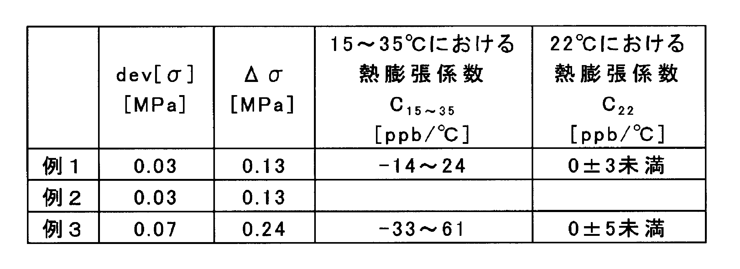
- Example 3 In a method for manufacturing a glass body, except that no performing step (e), to obtain a TiO 2 -SiO 2 glass substrate in the same manner as in Example 1. The results are shown in Tables 1 to 3.
- the TiO 2 -containing quartz glass substrate for imprint molds of the present invention is intended to form a fine concavo-convex pattern with a size of 1 nm to 10 ⁇ m in a semiconductor device, an optical waveguide, a micro optical element (diffraction grating, etc.), a biochip, a microreactor, etc. It is useful as a material for imprint molds used in the above.
- TiO 2 -containing quartz glass substrate for imprint mold 12 main surface 14 side surface 16 chamfered surface
Landscapes
- Engineering & Computer Science (AREA)
- Chemical & Material Sciences (AREA)
- Chemical Kinetics & Catalysis (AREA)
- Materials Engineering (AREA)
- Organic Chemistry (AREA)
- Mechanical Engineering (AREA)
- Manufacturing & Machinery (AREA)
- General Chemical & Material Sciences (AREA)
- Life Sciences & Earth Sciences (AREA)
- Geochemistry & Mineralogy (AREA)
- Physics & Mathematics (AREA)
- General Physics & Mathematics (AREA)
- Ceramic Engineering (AREA)
- Inorganic Chemistry (AREA)
- Thermal Sciences (AREA)
- Health & Medical Sciences (AREA)
- Ophthalmology & Optometry (AREA)
- Glass Compositions (AREA)
- Surface Treatment Of Glass (AREA)
- Exposure Of Semiconductors, Excluding Electron Or Ion Beam Exposure (AREA)
Abstract
Description
そして、発明者らの検討によりTiO2含有石英ガラス基材の側面の粗さやうねりが大きい場合、下記の問題が生じることがわかった。
(ii)TiO2含有石英ガラス基材の側面のうねりが大きいと、側面を研磨する際に用いた研磨砥粒(微粒子)が付着しやすく、(i)と同じ問題が生じる。また、インプリント法によってインプリントモールドの反転パターン(転写パターン)を基板の表面に転写する際に、モールドの側面を治具等に当接させて位置あわせしようとしても、側面のうねりによって位置がずれてしまう。そのため、インプリント法によって基板の表面に転写された凹凸パターンの位置もずれてしまう。
本発明のインプリントモールド用TiO2含有石英ガラス基材中のTiO2濃度は、3~12質量%であることが好ましい、
本発明のインプリントモールド用TiO2含有石英ガラス基材においては、ストリエによって生じる応力の最大値と最小値との差(Δσ)が、0.23MPa以下であることが好ましい。
本発明のインプリントモールド用TiO2含有石英ガラス基材の製造方法においては、前記TiO2含有石英ガラス基材が、前記主表面と前記側面との間に介在する面取り面を有する場合、TiO2含有石英ガラス基材の側面とともに面取り面を研磨することによって、前記面取り面の算術平均粗さ(Ra)を1nm以下とすることが好ましい。
本発明のインプリントモールド用TiO2含有石英ガラス基材の製造方法によれば、インプリントモールドとして用いた際に、インプリント法によって基板の表面に転写される凹凸パターンの欠陥や位置ズレを抑制できるインプリントモールド用TiO2含有石英ガラス基材を製造できる。
図1は、本発明のインプリントモールド用TiO2含有石英ガラス基材の一例を示す周縁付近の断面図である。
インプリントモールド用TiO2含有石英ガラス基材10は、2つの主表面12と、インプリントモールド用TiO2含有石英ガラス基材10の周縁に形成される側面14と、主表面12と側面14との間に介在する2つの面取り面16とを有する。
側面14の算術平均粗さ(Ra)は、1nm以下であり、0.7nm以下が好ましく、0.5nm以下がより好ましい。算術平均粗さ(Ra)が1nm以下であれば、側面14を研磨する際に用いた研磨砥粒等の微粒子が側面14に付着しにくい。また、側面にPVAスポンジを用いた擦り洗浄を行うことによって主表面に不具合を生じることなく微粒子を除去することが可能である。
算術平均粗さ(Ra)は、JIS B 0601:2001に規定される算術平均粗さ(Ra)であり、1μm×1μmの領域について原子間力顕微鏡(AFM)を用いて表面粗さを測定し、その結果から算出する。
側面14の、10μmから1mmの波長領域の凹凸の二乗平均平方根(MSFR_rms)は、10nm以下であり、7nm以下が好ましく、5nm以下がより好ましい。凹凸の二乗平均平方根(MSFR_rms)は側面14のうねりの指標であり、凹凸の二乗平均平方根(MSFR_rms)が10nm以下であれば、側面14を研磨する際に用いた研磨砥粒等の微粒子が側面14に付着しにくく、側面にPVAスポンジを用いた擦り洗浄を行うことによって主表面に不具合を生じることなく微粒子を除去することが可能である。また、インプリントモールドとした際に、側面14のうねりが原因となる位置ズレが生じにくい。
面取り面16の算術平均粗さ(Ra)は、1nm以下が好ましく、0.7nm以下がより好ましく、0.5nm以下がさらに好ましい。算術平均粗さ(Ra)が1nm以下であれば、面取り面16を研磨する際に用いた研磨砥粒等の微粒子が面取り面16に付着しにくい。また、側面にPVAスポンジを用いた擦り洗浄を行うことによって主表面に不具合を生じることなく微粒子を除去することが可能である。
インプリントモールド用TiO2含有石英ガラス基材10(100質量%)中のTiO2濃度は、3~12質量%が好ましい。インプリントモールド用TiO2含有石英ガラス基材10はインプリントモールド用基材として用いられるため、温度変化に対する寸法安定性が要求される。TiO2濃度が3~12質量%であれば、室温付近における熱膨張係数を小さくできる。室温付近における熱膨張係数をほぼゼロとするためには、TiO2濃度は、5~9質量%がより好ましく、6~8質量%がさらに好ましい。
TiO2濃度は、蛍光X線分析法において、ファンダメンタルパラメーター(FP)法を用いて測定する。
インプリントモールド用TiO2含有石英ガラス基材10中のTi3+濃度は、平均で、100質量ppm以下が好ましく、70質量ppm以下がより好ましく、20質量ppm以下がさらに好ましく、10質量ppm以下が特に好ましい。Ti3+濃度は、インプリントモールド用TiO2含有石英ガラスの着色、特に内部透過率T300~700に影響する。Ti3+濃度が100質量ppm以下であれば、茶色の着色が抑えられ、その結果、内部透過率T300~700の低下が抑えられ、透明性が良好となる。
出力:4mW、
変調磁場:100KHz、0.2mT、
測定温度:室温、
ESR種積分範囲:332~368mT、
感度校正:一定量のMn2+/MgOのピーク高さにて実施。
測定はサンプル主表面の中心点を通る任意のライン上で端から端まで10mmおきに行う。Ti3+濃度の最大値と最小値の差をΔTi3+とし、Ti3+濃度の平均値で除することでΔTi3+/Ti3+を求める。
インプリントモールド用TiO2含有石英ガラス基材10中のOH濃度は、600質量ppm未満が好ましく、400質量ppm以下がより好ましく、200質量ppm以下がさらに好ましく、100質量ppm以下が特に好ましい。OH濃度が600質量ppm未満であれば、OH基に起因する吸収による近赤外域における光透過率の低下が抑えられ、T300~3000が80%未満となりにくい。
赤外分光光度計による測定を行い、波長2.7μmでの吸収ピークからOH濃度を求める(J.P.Williams et.al.、Ceramic Bulletin、55(5)、524、1976)。該方法による検出限界は0.1質量ppmである。
インプリントモールド用TiO2含有石英ガラス基材10中のハロゲン濃度は、50質量ppm未満が好ましく、20質量ppm以下がより好ましく、1質量ppm以下がさらに好ましく、0.1質量ppm以下が特に好ましい。ハロゲン濃度が50質量ppm未満であれば、Ti3+濃度が増加しにくくなるため、茶色の着色が起こりにくくなる。その結果、T300~700の低下が抑えられ、透明性が損なわれない。
塩素濃度は、サンプルを水酸化ナトリウム溶液に加熱溶解し、陽イオン除去フィルタでろ過した溶解液について、イオンクロマトグラフ分析法にて塩素イオン濃度を定量分析することによって求める。
フッ素濃度は、フッ素イオン電極法によって求める。具体的には、日本化学会誌、1972(2)、350に記載された方法にしたがって、サンプルを無水炭酸ナトリウムに加熱融解し、得られた融液に蒸留水および塩酸(体積比で1:1)を加えて試料液を調製し、試料液の起電力をフッ素イオン選択性電極および比較電極としてラジオメータトレーディング社製No.945-220およびNo.945-468をそれぞれ用いてラジオメータによって測定し、フッ素イオン標準溶液を用いてあらかじめ作成した検量線に基づいて、フッ素濃度を求める。
インプリントモールド用TiO2含有石英ガラス基材10の、波長300~700nmの領域における厚さ1mmあたりの内部透過率T300~700は、70%以上が好ましく、80%以上がより好ましく、85%以上がさらに好ましい。光インプリント法では、紫外光照射によって光硬化性樹脂を硬化させるため、紫外光透過率が高い方が好ましい。
分光光度計を用いて、サンプル(鏡面研磨されたインプリントモールド用TiO2含有石英ガラス基材)の透過率を測定する。厚さ1mmあたりの内部透過率は、同じ程度の鏡面研磨を施した厚さの異なるサンプル、たとえば、厚さ2mmのサンプルと厚さ1mmのサンプルの透過率を測定し、透過率を吸光度に変換した後、厚さ2mmのサンプルの吸光度から厚さ1mmのサンプルの吸光度を引くことで、厚さ1mmあたりの吸光度を求め、再度透過率に変換することで求める。
内部透過率の測定波長域における厚さ1mmのサンプルの透過率を吸光度に変換し、前記石英ガラスの波長2000nm付近での吸光度を引く。吸光度の差を再度透過率に変換して内部透過率とする。
インプリントモールド用TiO2含有石英ガラス基材10の、ストリエによって生じる応力の標準偏差(dev[σ])は、0.05MPa以下が好ましく、0.04MPa以下がより好ましく、0.03MPa以下がさらに好ましい。通常、後述するスート法で製造されるガラス体は、3方向ストリエフリーといわれ、ストリエが見られないが、スート法で製造されるガラス体であってもドーパント(TiO2等)を含む場合には、ストリエが見られる可能性がある。ストリエが存在すると、研磨しても粗さやうねりの小さい表面が得られにくい。また、同様の理由から、インプリントモールド用TiO2含有石英ガラス基材10の、ストリエによって生じる応力における最大値と最小値との差(Δσ)は、0.23MPa以下が好ましく、0.2MPa以下がより好ましく、0.15MPa以下がさらに好ましい。
まず、複屈折顕微鏡を用いて1mm×1mm程度の領域を測定することでサンプルのレタデーションを求め、下式(1)から応力のプロファイルを求める。
Δ=C×F×n×d ・・・(1)。
ここで、Δは、レタデーションであり、Cは、光弾性定数であり、Fは、応力であり、nは屈折率であり、dは、サンプルの厚さである。
ついで、応力のプロファイルから、応力の標準偏差(dev[σ])、応力における最大値と最小値との差(Δσ)を求める。
具体的には、インプリントモールド用TiO2含有石英ガラス基材10からスライスによってサンプルを切り取り、さらに研磨を行うことによって、30mm×30mm×0.5mmの板状のサンプルを得る。複屈折顕微鏡にて、サンプルの30mm×30mmの面にヘリウムネオンレーザ光を垂直にあて、脈理が充分に観察可能な倍率に拡大して、面内のレタデーション分布を調べ、応力分布に換算する。脈理のピッチが細かい場合は、サンプルの厚さを薄くする必要がある。
インプリントモールド用TiO2含有石英ガラス基材10の、15~35℃における熱膨張係数C15~35は、0±200ppb/℃の範囲内にあることが好ましい。インプリントモールド用TiO2含有石英ガラス基材10は、インプリントモールド用基材として用いられるため、温度変化に対する寸法安定性、より具体的には、インプリント法の際に、該モールドが経験し得る温度領域における温度変化に対する寸法安定性に優れることが要求される。ここで、インプリントモールドが経験し得る温度領域は、インプリント法の種類によって異なる。光インプリント法では、紫外光照射によって光硬化性樹脂を硬化させるため、該モールドが経験し得る温度領域は基本的には室温付近である。ただし、紫外光照射によって該モールドの温度が局所的に上昇する場合がある。紫外光照射による局所的な温度上昇を考慮して、該モールドが経験し得る温度領域を15~35℃とする。C15~35は、0±100ppb/℃の範囲内にあることがより好ましく、0±50ppb/℃の範囲内にあることがさらに好ましく、0±30ppb/℃の範囲内にあることが特に好ましい。
インプリントモールド用TiO2含有石英ガラス基材10は、転写パターンを形成する側の主表面から深さ10μmまでの領域における仮想温度分布が±30℃以内のものが好ましく、該仮想温度分布が±20℃以内のものがより好ましく、該仮想温度分布が±10℃以内のものがさらに好ましい。該仮想温度分布が±30℃以内であれば、インプリントモールド用TiO2含有石英ガラス基材10の主表面にエッチングによって転写パターンを形成する際のエッチング速度のばらつきが抑えられる。
(i)仮想温度が未知のサンプルを用意する。該サンプルは、鏡面研磨されたインプリントモールド用TiO2含有石英ガラス基材10である。
(ii)仮想温度が既知で、かつ前記サンプルと組成が同じガラス体であって、仮想温度が異なる複数種類のガラス体を用意する。該ガラス体の表面は、鏡面研磨しておく。
(iii)赤外分光計(Nikolet社製Magna760)を用いて、前記(ii)のガラス体の表面の赤外反射スペクトルを取得する。反射スペクトルは、256回以上スキャンさせた平均値とする。得られた赤外反射スペクトルにおいて、約1120cm-1付近に観察されるピークがガラスのSi-O-Si結合による伸縮振動に起因するピークであり、ピーク位置は仮想温度に依存する。仮想温度が異なる複数種類のガラス体について得られた該ピーク位置と仮想温度との関係を示す検量線を作成する。
(iv)前記(i)のサンプルについて、前記(iii)と同じ条件にて赤外反射スペクトルを取得する。得られた赤外反射スペクトルにおいて、約1120cm-1付近に観察されるSi-O-Si結合による伸縮振動に起因するピークの位置を正確に求める。該ピーク位置を検量線に照らし合わせて、仮想温度を求める。
まず、前記の方法で表面の仮想温度を求める、ついで、10質量%フッ酸溶液に30秒間~1分間浸漬し、前後の質量減少量を求める。質量減少量から下式(2)によって、エッチングされた深さを求める。
(エッチングされた深さ)=(質量減少量)/((密度)×(表面積)) ・・・(2)。
また、前記の方法でエッチングして現れた表面の仮想温度を求め、その深さにおける仮想温度とする。その後、再度10質量%フッ酸溶液に30秒間~1分間浸漬し、深さと仮想温度を求める。これを繰り返して10μmを超える直前までの操作によって得られた仮想温度の値の中で最大値と最小値を決定しその差を、表面から深さ10μmまでの領域における仮想温度分布とする。
以上説明したインプリントモールド用TiO2含有石英ガラス基材10にあっては、側面14の算術平均粗さ(Ra)が1nm以下であり、側面14の、10μmから1mmの波長領域の凹凸の二乗平均平方根(MSFR_rms)が10nm以下であるため、側面14を研磨する際に用いた研磨砥粒等の微粒子が側面に付着しにくい。また、側面にPVAスポンジを用いた擦り洗浄を行うことによって主表面に不具合を生じることなく微粒子を除去することが可能である。その結果、インプリントモールド用TiO2含有石英ガラス基材10の側面14が擦れた際に微粒子が発生しにくくなり、側面研磨後の主表面研磨時に主表面に回り込み主表面にスクラッチを発生させる、バッチ式洗浄時に主表面に回り込み再付着する、といった不具合の発生を抑制できることによって、インプリント法によって基板の表面に転写される凹凸パターンにおける、微粒子、スクラッチが原因となって生じる欠陥が抑えられる。また、前記二乗平均平方根(MSFR_rms)が10nm以下であるため、インプリントモールドとした際に、側面14のうねりが原因となる位置ズレが生じにくい。その結果、インプリント法によって基板の表面に転写される凹凸パターンの位置ズレも抑えられる。
本発明のインプリントモールド用TiO2含有石英ガラス基材の製造方法は、(I)ストリエによって生じる応力の標準偏差(dev[σ])が0.05MPa以下、および/または(II)ストリエによって生じる応力の最大値と最小値との差(Δσ)が0.23MPa以下の、未研磨のTiO2含有石英ガラス基材の側面を研磨することによって、側面の算術平均粗さ(Ra)を1nm以下とし、側面の、10μmから1mmの波長領域の凹凸の二乗平均平方根(MSFR_rms)を10nm以下とする方法である。
インプリントモールド用TiO2含有石英ガラス基材(以下、TiO2-SiO2ガラス基材とも記す。)の製造方法としては、下記工程(a)~(f)を有する方法が挙げられる。
(b)前記多孔質TiO2-SiO2ガラス体を緻密化温度まで昇温してTiO2-SiO2緻密体を得る工程。
(c)前記TiO2-SiO2緻密体を透明ガラス化温度まで昇温して透明TiO2-SiO2ガラス体を得る工程。
(d)必要に応じて前記透明TiO2-SiO2ガラス体を軟化点以上に加熱して成形し、成形TiO2-SiO2ガラス体を得る工程。
(e)前記工程(c)で得られた透明TiO2-SiO2ガラス体または前記工程(d)で得られた成形TiO2-SiO2ガラス体をアニール処理する工程。
(f)前記工程(e)で得られたTiO2-SiO2ガラス体に、切断、切削、研磨等の機械加工を行うことにより、所定の形状を有するTiO2-SiO2ガラス基材を得る工程。
スート法によって、ガラス形成原料であるSiO2前駆体およびTiO2前駆体を火炎加水分解または熱分解させて得られるTiO2-SiO2ガラス微粒子(スート)を、ある一定速度で、軸を中心として回転する堆積用基材に堆積、成長させて多孔質TiO2-SiO2ガラス体を形成させる。
スート法としては、MCVD法、OVD法、VAD法等が挙げられ、大量生産性に優れる、堆積用基材の大きさ等の製造条件を調整することによって大面積の面内において組成の均一なガラス体が得られる、等の点から、VAD法が好ましい。
SiO2前駆体としては、ハロゲン化ケイ素化合物、アルコキシシランが挙げられる。
TiO2前駆体としては、ハロゲン化チタン化合物、アルコキシチタンが挙げられる。
アルコキシシランとしては、下式(3)で表わされる化合物が挙げられる。
RnSi(OR)4-n ・・・(3)。
ただし、Rは、炭素数1~4のアルキル基であり、nは、0~3の整数であり、複数のRにおいて、一部のRが異なっていてもよい。
アルコキシチタンとしては、下式(4)で表わされる化合物が挙げられる。
RnTi(OR)4-n ・・・(4)。
ただし、Rは、炭素数1~4のアルキル基であり、nは0~3の整数であり、複数のRにおいて、一部のRが異なっていてもよい。
堆積用基材としては、石英ガラス製の種棒(たとえば、日本国特公昭63-24937号公報に記載された種棒)が挙げられる。また、棒状に限らず、板状の堆積用基材を用いてもよい。
工程(a)で得られた多孔質TiO2-SiO2ガラス体を不活性ガス雰囲気中または減圧雰囲気下で緻密化温度まで昇温して、TiO2-SiO2緻密体を得る。
緻密化温度とは、光学顕微鏡で空隙が確認できなくなるまで多孔質TiO2-SiO2ガラス体を緻密化できる温度を意味する。
緻密化温度は、1250~1550℃が好ましく、1350~1450℃がより好ましい。
不活性ガスとしては、ヘリウムが好ましい。
雰囲気の圧力は、10000~200000Paが好ましい。本明細書におけるPaは、ゲージ圧ではなく絶対圧を意味する。
また、工程(b)においては、TiO2-SiO2緻密体の均質性が上がる点から、多孔質TiO2-SiO2ガラス体を不活性ガス雰囲気下、室温または緻密化温度未満の温度にて保持した後に、緻密化温度まで昇温することが好ましい。
工程(b)で得られたTiO2-SiO2緻密体を、透明ガラス化温度まで昇温して、透明TiO2-SiO2ガラス体を得る。
透明ガラス化温度とは、光学顕微鏡で結晶が確認できなくなり、透明なガラスが得られる温度を意味する。
透明ガラス化温度は、1350~1750℃が好ましく、1400~1700℃がより好ましい。
雰囲気としては、不活性ガス(ヘリウム、アルゴン等)の100%の雰囲気、または不活性ガス(ヘリウム、アルゴン等)を主成分とする雰囲気が好ましい。
雰囲気の圧力は、減圧または常圧が好ましい。減圧の場合は13000Pa以下が好ましい。
工程(c)で得られた透明TiO2-SiO2ガラス体を、型に入れて軟化点以上の温度に加熱して所望の形状に成形し、成形TiO2-SiO2ガラス体を得る。
成形温度は、1500~1800℃が好ましい。成形温度が1500℃以上であれば、透明TiO2-SiO2ガラス体の粘度が低くなり、自重変形しやすい。また、SiO2の結晶相であるクリストバライトの成長またはTiO2の結晶相であるルチルもしくはアナターゼの成長が抑えられ、いわゆる失透が生じにくい。成形温度が1800℃以下であれば、SiO2の昇華が抑えられる。
また、工程(c)および工程(d)を連続的に、または同時に行ってもよい。
また、工程(c)で得られた透明TiO2-SiO2ガラス体が充分に大きい場合は、つぎの工程(d)を行わずに工程(c)で得られた透明TiO2-SiO2ガラス体を所定の寸法に切り出すことで、成形TiO2-SiO2ガラス体としてもよい。
工程(d)の代わりにまたは工程(d)の後、工程(e)よりも前に、下記の工程(d')を行ってもよい。
(d')前記工程(c)で得られた透明TiO2-SiO2ガラス体または前記工程(d)で得られた成形TiO2-SiO2ガラス体を、T1+400℃以上の温度で20時間以上加熱する工程。
T1は、工程(e)で得られるTiO2-SiO2ガラス体の徐冷点(℃)である。徐冷点とは、ガラスの粘性ηが1013dPa・sとなる温度を意味する。徐冷点は、下記のように求める。
JIS R 3103-2:2001に準拠する方法でビームベンディング法によりガラスの粘性を測定し、粘性ηが1013dPa・sとなる温度を徐冷点とする。
ストリエとは、TiO2-SiO2ガラス体の組成上の不均一(組成分布)である。ストリエを有するTiO2-SiO2ガラス体にはTiO2濃度の異なる部位が存在することになる。TiO2濃度が高い部位は、熱膨張係数(CTE)が負になるため、工程(e)における降温過程の際に、TiO2濃度が高い部位が膨張する傾向がある。この際、TiO2濃度が高い部位に隣接してTiO2濃度が低い部位が存在すると、TiO2濃度が高い部位の膨張が妨げられて圧縮応力が加わることとなる。その結果、TiO2-SiO2ガラス体には応力の分布が生じることとなる。本明細書において、このような応力の分布のことを「ストリエによって生じる応力の分布」という。
工程(d)または(d')を行うことによって、ついで行われる工程(e)を経て製造されるTiO2-SiO2ガラス体におけるストリエによって生じる応力の分布が、インプリントモールド用基材として用いる上で問題とならないレベルまで低減される。
また、工程(c)およびまたは工程(d)と、工程(d')とを連続的に、または同時に行ってもよい。
工程(c)で得られた透明TiO2-SiO2ガラス体、工程(d)で得られた成形TiO2-SiO2ガラス体、または工程(d’)で得られたTiO2-SiO2ガラス体を、1100℃以上の温度に昇温した後、100℃/hr以下の平均降温速度で700℃以下の温度まで降温するアニール処理を行い、TiO2-SiO2ガラス体の仮想温度を制御する。
また、700℃以下の温度まで降温した後は放冷できる。なお、雰囲気は特に限定されない。
工程(e)で得られたTiO2-SiO2ガラス体に、切断、切削、研磨等の機械加工を行うことにより、所定の形状を有するTiO2-SiO2ガラス基材を得る。本発明においては、少なくとも研磨を行う。
研磨工程はその研磨面の仕上がり状況に応じて2回以上の工程に分けて行うことが好ましい。最終研磨工程においては、研磨剤としてコロイダルシリカを用いることが好ましい。
以上説明した本発明のインプリントモールド用TiO2含有石英ガラス基材の製造方法にあっては、(I)ストリエによって生じる応力の標準偏差(dev[σ])が0.05MPa以下、および/または(II)ストリエによって生じる応力の最大値と最小値との差(Δσ)が0.23MPa以下、すなわちストリエの小さいTiO2含有石英ガラス基材の側面を研磨しているため、側面の算術平均粗さ(Ra)を1nm以下とし、側面の、10μmから1mmの波長領域の凹凸の二乗平均平方根(MSFR_rms)を10nm以下とすることができる。
また、研磨砥粒を含む研磨液を供給しながら、研磨用のブラシ毛が突設された研磨ブラシとTiO2含有石英ガラス基材とを相対的に移動させて、TiO2含有石英ガラス基材の側面を研磨することによって、側面の算術平均粗さ(Ra)を1nm以下とし、側面の、10μmから1mmの波長領域の凹凸の二乗平均平方根(MSFR_rms)を10nm以下とすることができる。
インプリントモールドは、本発明のインプリントモールド用TiO2含有石英ガラス基材の主表面に、エッチングによって転写パターンを形成することによって製造できる。
転写パターンは、目的とする微細な凹凸パターンの反転パターンであり、複数の微細な凸部および/または凹部からなる。
エッチング方法としては、ドライエッチングが好ましく、具体的には、SF6による反応性イオンエッチングが好ましい。
例1、2は実施例であり、例3は比較例である。
(工程(a))
ガラス形成原料であるTiCl4およびSiCl4を、それぞれガス化させた後に混合し、酸水素火炎中で加熱加水分解(火炎加水分解)させることで得られるTiO2-SiO2ガラス微粒子を堆積用基材に堆積、成長させて、多孔質TiO2-SiO2ガラス体を形成した。
得られた多孔質TiO2-SiO2ガラス体はそのままではハンドリングしにくいため、堆積用基材に堆積させたままの状態で、大気中、1200℃にて4時間保持した後、堆積用基材から外した。
得られた多孔質TiO2-SiO2ガラス体を、減圧下にて1450℃で4時間保持して、TiO2-SiO2緻密体を得た。
得られたTiO2-SiO2緻密体を、カーボン型に入れて1680℃にて4時間保持することによって透明TiO2-SiO2ガラス体を得た。
得られた透明TiO2-SiO2ガラス体を、再度カーボン型に入れて、1700℃にて4時間保持することによって成形TiO2-SiO2ガラス体を得た。
得られた成形TiO2-SiO2ガラス体を、そのまま炉内で1000℃まで10℃/hrで冷却した後、1000℃で3時間保持し、950℃まで10℃/hrで冷却した後、950℃で72時間保持し、900℃まで5℃/hrで冷却した後、900℃で72時間保持した後、700℃まで100℃/hrで冷却し、その後室温まで放冷してTiO2-SiO2ガラス体を得た。
得られたTiO2-SiO2ガラス体について、TiO2濃度、Ti3+濃度、ΔTi3+/Ti3+、OH濃度、ハロゲン濃度、内部透過率、応力、熱膨張係数を、上述の方法にて求めた。結果を表1および表2に示す。なお、工程(e)で得られたTiO2-SiO2についてのデータは、後述の工程(f)における切断、切削、研磨等によって変化することはない。
得られたTiO2-SiO2ガラス体を、内周刃スライサーを用いて縦約153.0mm×横約153.0mm×厚さ約6.75mmの板状に切断し、未研磨のTiO2-SiO2ガラス板を作製した。
該TiO2-SiO2ガラス板に、市販のNC面取り機を用い、#120のダイアモンド砥石によって、縦、横の外形寸法が約152mmで面取り幅が0.2~0.4mmになるように、面取り加工を施した。20B両面ラップ機(スピードファム社製)を用い、研磨材である#400のSiCによって、厚さが約6.50mmになるまで、TiO2-SiO2ガラス板の主表面を研磨した。
2次ポリシュとして、20B両面ポリシュ機を用い、研磨材である平均粒径1.0umの酸化セリウムを主成分とするスラリによって、主表面を約10μm研磨した。
3次ポリシュとして、別の研磨機を用いて最終研磨を行った。最終研磨においては、研磨剤としてコロイダルシリカ(フジミコーポレーション製、コンポール20)を用いた。
研磨後のTiO2-SiO2ガラス板を、第一槽目を硫酸と過酸化水素水の熱溶液、第三槽目を中性界面活性剤溶液とした多段式自動洗浄機を用いて洗浄した。
得られたTiO2-SiO2ガラス基材について、仮想温度分布、側面の算術平均粗さ、凹凸の二乗平均平方根、面取り面の算術平均粗さを、上述の方法にて求めた。結果を表3に示す。
振動試験後、収納ケースをクリーンルーム内で開封し、取り出したTiO2-SiO2ガラス基材について、欠陥検査装置(レーザーテック社製、M1320)を用いて主表面における付着異物による欠陥個数を測定し、下記の基準にて評価する。結果を表3に示す。
A:振動試験前後で欠陥個数にほとんど差は認められない。
B:振動試験前に比べ振動試験後の欠陥個数が明らかに増加した。
工程(f)のTiO2-SiO2ガラス板の側面および面取り面の研磨をロール状の支持体に外周方向に向けてブラシが突設された研磨ブラシを用い、TiO2-SiO2ガラス板を主表面に垂直な軸を回転軸として回転させ、回転させたロール状ブラシに接触させることによって行う以外は、例1と同様にしてTiO2-SiO2ガラス基材を得る。結果を表1~3に示す。
ガラス体の作製方法において、工程(e)を実施しないこと以外は、例1と同様にしてTiO2-SiO2ガラス基材を得る。結果を表1~3に示す。


本出願は、2010年7月12日出願の、日本特許出願2010-157811に基づくものであり、その内容はここに参照として取り込まれる。
12 主表面
14 側面
16 面取り面
Claims (9)
- 主表面と側面とを有する、インプリントモールド用TiO2含有石英ガラス基材であって、
前記側面の算術平均粗さ(Ra)が、1nm以下であり、
前記側面の、10μmから1mmの波長領域の凹凸の二乗平均平方根(MSFR_rms)が、10nm以下である、インプリントモールド用TiO2含有石英ガラス基材。 - 前記主表面と前記側面との間に介在する面取り面を有し、
前記面取り面の算術平均粗さ(Ra)が、1nm以下である、請求項1に記載のインプリントモールド用TiO2含有石英ガラス基材。 - TiO2濃度が、3~12質量%である、請求項1または2に記載のインプリントモールド用TiO2含有石英ガラス基材。
- ストリエによって生じる応力の標準偏差(dev[σ])が、0.05MPa以下である、請求項1~3のいずれかに記載のインプリントモールド用TiO2含有石英ガラス基材。
- ストリエによって生じる応力の最大値と最小値との差(Δσ)が、0.23MPa以下である、請求項1~4のいずれかに記載のインプリントモールド用TiO2含有石英ガラス基材。
- 主表面と側面とを有する、インプリントモールド用TiO2含有石英ガラス基材を製造する方法であって、
ストリエによって生じる応力の標準偏差(dev[σ])が0.05MPa以下のTiO2含有石英ガラス基材の側面を研磨することによって、
前記側面の算術平均粗さ(Ra)を1nm以下とし、
前記側面の、10μmから1mmの波長領域の凹凸の二乗平均平方根(MSFR_rms)を10nm以下とする、インプリントモールド用TiO2含有石英ガラス基材の製造方法。 - 主表面と側面とを有する、インプリントモールド用TiO2含有石英ガラス基材を製造する方法であって、
ストリエによって生じる応力の最大値と最小値との差(Δσ)が0.23MPa以下のTiO2含有石英ガラス基材の側面を研磨することによって、
前記側面の算術平均粗さ(Ra)を1nm以下とし、
前記側面の、10μmから1mmの波長領域の凹凸の二乗平均平方根(MSFR_rms)を10nm以下とする、インプリントモールド用TiO2含有石英ガラス基材の製造方法。 - 研磨砥粒を含む研磨液を供給しながら、研磨用のブラシ毛が突設された研磨ブラシと前記TiO2含有石英ガラス基材とを相対的に移動させて、前記TiO2含有石英ガラス基材の側面を研磨する、請求項6または7に記載のインプリントモールド用TiO2含有石英ガラス基材の製造方法。
- 前記TiO2含有石英ガラス基材が、前記主表面と前記側面との間に介在する面取り面を有し、
TiO2含有石英ガラス基材の側面とともに面取り面を研磨することによって、
前記面取り面の算術平均粗さ(Ra)を1nm以下とする、請求項6~8のいずれかに記載のインプリントモールド用TiO2含有石英ガラス基材の製造方法。
Priority Applications (5)
| Application Number | Priority Date | Filing Date | Title |
|---|---|---|---|
| KR1020137000575A KR20130091313A (ko) | 2010-07-12 | 2011-07-06 | 임프린트 몰드용 TiO₂함유 석영 유리 기재 및 그 제조 방법 |
| CN201180034592.3A CN103003054B (zh) | 2010-07-12 | 2011-07-06 | 压印模具用含TiO2石英玻璃基材及其制造方法 |
| JP2012524525A JP5772827B2 (ja) | 2010-07-12 | 2011-07-06 | インプリントモールド用TiO2含有石英ガラス基材およびその製造方法 |
| US13/740,786 US20130149494A1 (en) | 2010-07-12 | 2013-01-14 | TiO2-CONTAINING QUARTZ-GLASS SUBSTRATE FOR AN IMPRINT MOLD AND MANUFACTURING METHOD THEREFOR |
| US14/570,340 US20150097304A1 (en) | 2010-07-12 | 2014-12-15 | TiO2-CONTAINING QUARTZ-GLASS SUBSTRATE FOR AN IMPRINT MOLD AND MANUFACTURING METHOD THEREFOR |
Applications Claiming Priority (2)
| Application Number | Priority Date | Filing Date | Title |
|---|---|---|---|
| JP2010157811 | 2010-07-12 | ||
| JP2010-157811 | 2010-07-12 |
Related Child Applications (1)
| Application Number | Title | Priority Date | Filing Date |
|---|---|---|---|
| US13/740,786 Continuation US20130149494A1 (en) | 2010-07-12 | 2013-01-14 | TiO2-CONTAINING QUARTZ-GLASS SUBSTRATE FOR AN IMPRINT MOLD AND MANUFACTURING METHOD THEREFOR |
Publications (1)
| Publication Number | Publication Date |
|---|---|
| WO2012008343A1 true WO2012008343A1 (ja) | 2012-01-19 |
Family
ID=45469346
Family Applications (1)
| Application Number | Title | Priority Date | Filing Date |
|---|---|---|---|
| PCT/JP2011/065497 Ceased WO2012008343A1 (ja) | 2010-07-12 | 2011-07-06 | インプリントモールド用TiO2含有石英ガラス基材およびその製造方法 |
Country Status (6)
| Country | Link |
|---|---|
| US (2) | US20130149494A1 (ja) |
| JP (1) | JP5772827B2 (ja) |
| KR (1) | KR20130091313A (ja) |
| CN (1) | CN103003054B (ja) |
| TW (1) | TWI531458B (ja) |
| WO (1) | WO2012008343A1 (ja) |
Cited By (5)
| Publication number | Priority date | Publication date | Assignee | Title |
|---|---|---|---|---|
| JP2013211450A (ja) * | 2012-03-30 | 2013-10-10 | Dainippon Printing Co Ltd | 基板の製造方法、および、ナノインプリントリソグラフィ用テンプレートの製造方法 |
| JP2016043692A (ja) * | 2014-08-19 | 2016-04-04 | 信越化学工業株式会社 | インプリント・リソグラフィ用角形基板及びその製造方法 |
| JP2016113356A (ja) * | 2014-12-12 | 2016-06-23 | 旭硝子株式会社 | 予備研磨されたガラス基板表面を仕上げ加工する方法 |
| JP2018035058A (ja) * | 2016-08-25 | 2018-03-08 | 信越化学工業株式会社 | 角型ガラス基板及びその製造方法 |
| JP2018076204A (ja) * | 2016-11-10 | 2018-05-17 | 旭硝子株式会社 | 半導体用ガラス基板及び非貫通穴を有する半導体用ガラス基板の製造方法 |
Families Citing this family (39)
| Publication number | Priority date | Publication date | Assignee | Title |
|---|---|---|---|---|
| EP2532508A4 (en) * | 2010-02-03 | 2014-01-08 | Asahi Glass Co Ltd | METHOD FOR PRODUCING AN ARTICLE WITH A FINISHED SURFACE STRUCTURE |
| WO2014079478A1 (en) | 2012-11-20 | 2014-05-30 | Light In Light Srl | High speed laser processing of transparent materials |
| EP2754524B1 (de) | 2013-01-15 | 2015-11-25 | Corning Laser Technologies GmbH | Verfahren und Vorrichtung zum laserbasierten Bearbeiten von flächigen Substraten, d.h. Wafer oder Glaselement, unter Verwendung einer Laserstrahlbrennlinie |
| EP2781296B1 (de) | 2013-03-21 | 2020-10-21 | Corning Laser Technologies GmbH | Vorrichtung und verfahren zum ausschneiden von konturen aus flächigen substraten mittels laser |
| US10442719B2 (en) | 2013-12-17 | 2019-10-15 | Corning Incorporated | Edge chamfering methods |
| US11556039B2 (en) | 2013-12-17 | 2023-01-17 | Corning Incorporated | Electrochromic coated glass articles and methods for laser processing the same |
| US10293436B2 (en) | 2013-12-17 | 2019-05-21 | Corning Incorporated | Method for rapid laser drilling of holes in glass and products made therefrom |
| US9676167B2 (en) | 2013-12-17 | 2017-06-13 | Corning Incorporated | Laser processing of sapphire substrate and related applications |
| US20150165560A1 (en) | 2013-12-17 | 2015-06-18 | Corning Incorporated | Laser processing of slots and holes |
| US9701563B2 (en) | 2013-12-17 | 2017-07-11 | Corning Incorporated | Laser cut composite glass article and method of cutting |
| US9815730B2 (en) | 2013-12-17 | 2017-11-14 | Corning Incorporated | Processing 3D shaped transparent brittle substrate |
| US9850160B2 (en) | 2013-12-17 | 2017-12-26 | Corning Incorporated | Laser cutting of display glass compositions |
| KR102432658B1 (ko) * | 2014-01-27 | 2022-08-16 | 코닝 인코포레이티드 | 레이저 컷팅 유리를 기계적으로 처리하여 챔퍼링된 에지 |
| KR102445217B1 (ko) | 2014-07-08 | 2022-09-20 | 코닝 인코포레이티드 | 재료를 레이저 가공하는 방법 및 장치 |
| LT3169477T (lt) * | 2014-07-14 | 2020-05-25 | Corning Incorporated | Skaidrių medžiagų apdorojimo sistema ir būdas, naudojant lazerio pluošto židinio linijas, kurių ilgis ir skersmuo yra reguliuojami |
| EP3536440A1 (en) | 2014-07-14 | 2019-09-11 | Corning Incorporated | Glass article with a defect pattern |
| WO2016010991A1 (en) | 2014-07-14 | 2016-01-21 | Corning Incorporated | Interface block; system for and method of cutting a substrate being transparent within a range of wavelengths using such interface block |
| WO2016010949A1 (en) | 2014-07-14 | 2016-01-21 | Corning Incorporated | Method and system for forming perforations |
| US10047001B2 (en) | 2014-12-04 | 2018-08-14 | Corning Incorporated | Glass cutting systems and methods using non-diffracting laser beams |
| JP2018507154A (ja) | 2015-01-12 | 2018-03-15 | コーニング インコーポレイテッド | マルチフォトン吸収方法を用いた熱強化基板のレーザー切断 |
| WO2016154284A1 (en) | 2015-03-24 | 2016-09-29 | Corning Incorporated | Laser cutting and processing of display glass compositions |
| CN107666983B (zh) | 2015-03-27 | 2020-10-02 | 康宁股份有限公司 | 可透气窗及其制造方法 |
| KR102499697B1 (ko) | 2015-07-10 | 2023-02-14 | 코닝 인코포레이티드 | 유연한 기판 시트에서의 홀의 연속 제조 방법 및 이에 관한 물품 |
| KR102405144B1 (ko) | 2016-05-06 | 2022-06-07 | 코닝 인코포레이티드 | 투명 기판들로부터의 윤곽 형상들의 레이저 절단 및 제거 |
| US10410883B2 (en) | 2016-06-01 | 2019-09-10 | Corning Incorporated | Articles and methods of forming vias in substrates |
| US10794679B2 (en) | 2016-06-29 | 2020-10-06 | Corning Incorporated | Method and system for measuring geometric parameters of through holes |
| JP7090594B2 (ja) | 2016-07-29 | 2022-06-24 | コーニング インコーポレイテッド | レーザ加工するための装置および方法 |
| US10522963B2 (en) | 2016-08-30 | 2019-12-31 | Corning Incorporated | Laser cutting of materials with intensity mapping optical system |
| WO2018064409A1 (en) | 2016-09-30 | 2018-04-05 | Corning Incorporated | Apparatuses and methods for laser processing transparent workpieces using non-axisymmetric beam spots |
| LT3529214T (lt) | 2016-10-24 | 2021-02-25 | Corning Incorporated | Substrato apdorojimo stotis lakšto formos stiklo substratų lazeriniam mašininiam apdorojimui |
| US10752534B2 (en) | 2016-11-01 | 2020-08-25 | Corning Incorporated | Apparatuses and methods for laser processing laminate workpiece stacks |
| US10688599B2 (en) | 2017-02-09 | 2020-06-23 | Corning Incorporated | Apparatus and methods for laser processing transparent workpieces using phase shifted focal lines |
| US10580725B2 (en) | 2017-05-25 | 2020-03-03 | Corning Incorporated | Articles having vias with geometry attributes and methods for fabricating the same |
| US11078112B2 (en) | 2017-05-25 | 2021-08-03 | Corning Incorporated | Silica-containing substrates with vias having an axially variable sidewall taper and methods for forming the same |
| US10626040B2 (en) | 2017-06-15 | 2020-04-21 | Corning Incorporated | Articles capable of individual singulation |
| US12180108B2 (en) | 2017-12-19 | 2024-12-31 | Corning Incorporated | Methods for etching vias in glass-based articles employing positive charge organic molecules |
| US11554984B2 (en) | 2018-02-22 | 2023-01-17 | Corning Incorporated | Alkali-free borosilicate glasses with low post-HF etch roughness |
| JP7122997B2 (ja) * | 2019-04-05 | 2022-08-22 | 信越石英株式会社 | 紫外線吸収性に優れたチタン含有石英ガラス及びその製造方法 |
| EP4252045A4 (en) * | 2020-11-24 | 2025-01-22 | Applied Materials, Inc. | PLANARIZED CRYSTALLINE LAYERS FOR DIFFRACTIVE OPTICS |
Citations (7)
| Publication number | Priority date | Publication date | Assignee | Title |
|---|---|---|---|---|
| JP2004315351A (ja) * | 2003-04-03 | 2004-11-11 | Asahi Glass Co Ltd | TiO2を含有するシリカガラスおよびEUVリソグラフィ用光学部材 |
| JP2008266046A (ja) * | 2007-04-17 | 2008-11-06 | Nippon Electric Glass Co Ltd | フラットパネルディスプレイ用ガラス基板およびその製造方法 |
| JP2008303100A (ja) * | 2007-06-06 | 2008-12-18 | Shin Etsu Chem Co Ltd | ナノインプリントモールド用チタニアドープ石英ガラス |
| JP2009013048A (ja) * | 2007-06-06 | 2009-01-22 | Shin Etsu Chem Co Ltd | ナノインプリントモールド用チタニアドープ石英ガラス |
| WO2009034954A1 (ja) * | 2007-09-13 | 2009-03-19 | Asahi Glass Co., Ltd. | TiO2含有石英ガラス基板 |
| JP2010502538A (ja) * | 2006-09-05 | 2010-01-28 | 旭硝子株式会社 | 石英ガラス基板およびその製造方法 |
| WO2011068100A1 (ja) * | 2009-12-04 | 2011-06-09 | 旭硝子株式会社 | インプリントモールド用石英系ガラス基材の製造方法およびインプリントモールドの製造方法 |
Family Cites Families (12)
| Publication number | Priority date | Publication date | Assignee | Title |
|---|---|---|---|---|
| JP3046003B2 (ja) * | 1998-08-10 | 2000-05-29 | ホーヤ株式会社 | 電子デバイス用ガラス基板及びその製造方法 |
| US7053017B2 (en) * | 2002-03-05 | 2006-05-30 | Corning Incorporated | Reduced striae extreme ultraviolet elements |
| CN100429067C (zh) * | 2003-05-23 | 2008-10-29 | 大日本印刷株式会社 | 光学片的制造方法和光学片 |
| JP4979941B2 (ja) * | 2005-03-30 | 2012-07-18 | Hoya株式会社 | マスクブランクス用ガラス基板の製造方法、マスクブランクスの製造方法 |
| JP4781003B2 (ja) * | 2005-04-28 | 2011-09-28 | 信越石英株式会社 | ナノインプリントスタンパー用シリカ・チタニアガラス |
| JP2008132699A (ja) * | 2006-11-29 | 2008-06-12 | Sumitomo Chemical Co Ltd | 表面形状転写樹脂シートの製造方法 |
| EP2212745A1 (en) * | 2007-11-01 | 2010-08-04 | 3M Innovative Properties Company | Method for replicating master molds |
| JP5314901B2 (ja) * | 2008-02-13 | 2013-10-16 | 国立大学法人東北大学 | シリカ・チタニアガラス及びその製造方法、線膨張係数測定方法 |
| WO2009107858A1 (en) * | 2008-02-26 | 2009-09-03 | Asahi Glass Co., Ltd. | Tio2-containing silica glass and optical member for euv lithography using high energy densities as well as special temperature controlled process for its manufacture |
| EP2256789B1 (en) * | 2008-03-18 | 2012-07-04 | Asahi Glass Company, Limited | Reflective mask blank for euv lithography |
| JP2010135732A (ja) * | 2008-08-01 | 2010-06-17 | Asahi Glass Co Ltd | Euvマスクブランクス用基板 |
| JP2010087188A (ja) * | 2008-09-30 | 2010-04-15 | Toshiba Corp | 転写原版の製造方法、及び半導体装置の製造方法 |
-
2011
- 2011-07-06 WO PCT/JP2011/065497 patent/WO2012008343A1/ja not_active Ceased
- 2011-07-06 JP JP2012524525A patent/JP5772827B2/ja active Active
- 2011-07-06 CN CN201180034592.3A patent/CN103003054B/zh not_active Expired - Fee Related
- 2011-07-06 KR KR1020137000575A patent/KR20130091313A/ko not_active Ceased
- 2011-07-12 TW TW100124645A patent/TWI531458B/zh not_active IP Right Cessation
-
2013
- 2013-01-14 US US13/740,786 patent/US20130149494A1/en not_active Abandoned
-
2014
- 2014-12-15 US US14/570,340 patent/US20150097304A1/en not_active Abandoned
Patent Citations (7)
| Publication number | Priority date | Publication date | Assignee | Title |
|---|---|---|---|---|
| JP2004315351A (ja) * | 2003-04-03 | 2004-11-11 | Asahi Glass Co Ltd | TiO2を含有するシリカガラスおよびEUVリソグラフィ用光学部材 |
| JP2010502538A (ja) * | 2006-09-05 | 2010-01-28 | 旭硝子株式会社 | 石英ガラス基板およびその製造方法 |
| JP2008266046A (ja) * | 2007-04-17 | 2008-11-06 | Nippon Electric Glass Co Ltd | フラットパネルディスプレイ用ガラス基板およびその製造方法 |
| JP2008303100A (ja) * | 2007-06-06 | 2008-12-18 | Shin Etsu Chem Co Ltd | ナノインプリントモールド用チタニアドープ石英ガラス |
| JP2009013048A (ja) * | 2007-06-06 | 2009-01-22 | Shin Etsu Chem Co Ltd | ナノインプリントモールド用チタニアドープ石英ガラス |
| WO2009034954A1 (ja) * | 2007-09-13 | 2009-03-19 | Asahi Glass Co., Ltd. | TiO2含有石英ガラス基板 |
| WO2011068100A1 (ja) * | 2009-12-04 | 2011-06-09 | 旭硝子株式会社 | インプリントモールド用石英系ガラス基材の製造方法およびインプリントモールドの製造方法 |
Cited By (7)
| Publication number | Priority date | Publication date | Assignee | Title |
|---|---|---|---|---|
| JP2013211450A (ja) * | 2012-03-30 | 2013-10-10 | Dainippon Printing Co Ltd | 基板の製造方法、および、ナノインプリントリソグラフィ用テンプレートの製造方法 |
| JP2016043692A (ja) * | 2014-08-19 | 2016-04-04 | 信越化学工業株式会社 | インプリント・リソグラフィ用角形基板及びその製造方法 |
| US11904521B2 (en) | 2014-08-19 | 2024-02-20 | Shin-Etsu Chemical Co., Ltd. | Rectangular substrate for imprint lithography and making method |
| JP2016113356A (ja) * | 2014-12-12 | 2016-06-23 | 旭硝子株式会社 | 予備研磨されたガラス基板表面を仕上げ加工する方法 |
| JP2018035058A (ja) * | 2016-08-25 | 2018-03-08 | 信越化学工業株式会社 | 角型ガラス基板及びその製造方法 |
| US10829411B2 (en) | 2016-08-25 | 2020-11-10 | Shin-Etsu Chemical Co., Ltd. | Rectangular glass substrate and method for preparing the same |
| JP2018076204A (ja) * | 2016-11-10 | 2018-05-17 | 旭硝子株式会社 | 半導体用ガラス基板及び非貫通穴を有する半導体用ガラス基板の製造方法 |
Also Published As
| Publication number | Publication date |
|---|---|
| US20150097304A1 (en) | 2015-04-09 |
| JPWO2012008343A1 (ja) | 2013-09-09 |
| TWI531458B (zh) | 2016-05-01 |
| KR20130091313A (ko) | 2013-08-16 |
| CN103003054B (zh) | 2014-11-19 |
| JP5772827B2 (ja) | 2015-09-02 |
| US20130149494A1 (en) | 2013-06-13 |
| TW201206677A (en) | 2012-02-16 |
| CN103003054A (zh) | 2013-03-27 |
Similar Documents
| Publication | Publication Date | Title |
|---|---|---|
| JP5772827B2 (ja) | インプリントモールド用TiO2含有石英ガラス基材およびその製造方法 | |
| JP4957249B2 (ja) | TiO2を含有するシリカガラスおよびその製造方法 | |
| JP5676718B2 (ja) | Euvマスクブランクス用基板 | |
| EP2463250B1 (en) | Methods for producing and for heat-treating a tio2-sio2 glass body | |
| JP5796598B2 (ja) | 凹凸パターン形成方法 | |
| KR101740067B1 (ko) | TiO₂를 함유하는 실리카 유리를 포함하는 광학 부재 | |
| KR20100118125A (ko) | TiO₂ 함유 실리카 유리 및 이를 사용한 리소그래피용 광학 부재 | |
| EP2468692A1 (en) | Tio2-containing silicia glass, and optical member for euv lithography | |
| JP5942848B2 (ja) | TiO2含有石英ガラス基材 | |
| KR20100005679A (ko) | 티타니아 도핑 석영 유리 부재 및 그의 제조 방법 | |
| JP5637146B2 (ja) | インプリントモールド用石英系ガラス基材の製造方法およびインプリントモールドの製造方法 | |
| EP2441736A1 (en) | Method for producing tio2-sio2 glass body,method for heat-treating tio2-sio2 glass body,tio2-sio2 glass body,and optical base for euvl | |
| WO2011002068A1 (ja) | ArFリソグラフィ用ミラー、およびArFリソグラフィ用光学部材 | |
| JP5287271B2 (ja) | TiO2を含有するシリカガラスの成型方法およびそれによって成型されたEUVリソグラフィ用光学部材 |
Legal Events
| Date | Code | Title | Description |
|---|---|---|---|
| 121 | Ep: the epo has been informed by wipo that ep was designated in this application |
Ref document number: 11806673 Country of ref document: EP Kind code of ref document: A1 |
|
| WWE | Wipo information: entry into national phase |
Ref document number: 2012524525 Country of ref document: JP |
|
| ENP | Entry into the national phase |
Ref document number: 20137000575 Country of ref document: KR Kind code of ref document: A |
|
| NENP | Non-entry into the national phase |
Ref country code: DE |
|
| 122 | Ep: pct application non-entry in european phase |
Ref document number: 11806673 Country of ref document: EP Kind code of ref document: A1 |