WO2012008003A1 - 多結晶シリコンの鋳造方法 - Google Patents
多結晶シリコンの鋳造方法 Download PDFInfo
- Publication number
- WO2012008003A1 WO2012008003A1 PCT/JP2010/006919 JP2010006919W WO2012008003A1 WO 2012008003 A1 WO2012008003 A1 WO 2012008003A1 JP 2010006919 W JP2010006919 W JP 2010006919W WO 2012008003 A1 WO2012008003 A1 WO 2012008003A1
- Authority
- WO
- WIPO (PCT)
- Prior art keywords
- raw material
- particle size
- polycrystalline silicon
- crucible
- silicon
- Prior art date
- Legal status (The legal status is an assumption and is not a legal conclusion. Google has not performed a legal analysis and makes no representation as to the accuracy of the status listed.)
- Ceased
Links
Images

Classifications
-
- C—CHEMISTRY; METALLURGY
- C30—CRYSTAL GROWTH
- C30B—SINGLE-CRYSTAL GROWTH; UNIDIRECTIONAL SOLIDIFICATION OF EUTECTIC MATERIAL OR UNIDIRECTIONAL DEMIXING OF EUTECTOID MATERIAL; REFINING BY ZONE-MELTING OF MATERIAL; PRODUCTION OF A HOMOGENEOUS POLYCRYSTALLINE MATERIAL WITH DEFINED STRUCTURE; SINGLE CRYSTALS OR HOMOGENEOUS POLYCRYSTALLINE MATERIAL WITH DEFINED STRUCTURE; AFTER-TREATMENT OF SINGLE CRYSTALS OR A HOMOGENEOUS POLYCRYSTALLINE MATERIAL WITH DEFINED STRUCTURE; APPARATUS THEREFOR
- C30B29/00—Single crystals or homogeneous polycrystalline material with defined structure characterised by the material or by their shape
- C30B29/02—Elements
- C30B29/06—Silicon
-
- C—CHEMISTRY; METALLURGY
- C30—CRYSTAL GROWTH
- C30B—SINGLE-CRYSTAL GROWTH; UNIDIRECTIONAL SOLIDIFICATION OF EUTECTIC MATERIAL OR UNIDIRECTIONAL DEMIXING OF EUTECTOID MATERIAL; REFINING BY ZONE-MELTING OF MATERIAL; PRODUCTION OF A HOMOGENEOUS POLYCRYSTALLINE MATERIAL WITH DEFINED STRUCTURE; SINGLE CRYSTALS OR HOMOGENEOUS POLYCRYSTALLINE MATERIAL WITH DEFINED STRUCTURE; AFTER-TREATMENT OF SINGLE CRYSTALS OR A HOMOGENEOUS POLYCRYSTALLINE MATERIAL WITH DEFINED STRUCTURE; APPARATUS THEREFOR
- C30B11/00—Single-crystal growth by normal freezing or freezing under temperature gradient, e.g. Bridgman-Stockbarger method
- C30B11/001—Continuous growth
-
- Y—GENERAL TAGGING OF NEW TECHNOLOGICAL DEVELOPMENTS; GENERAL TAGGING OF CROSS-SECTIONAL TECHNOLOGIES SPANNING OVER SEVERAL SECTIONS OF THE IPC; TECHNICAL SUBJECTS COVERED BY FORMER USPC CROSS-REFERENCE ART COLLECTIONS [XRACs] AND DIGESTS
- Y02—TECHNOLOGIES OR APPLICATIONS FOR MITIGATION OR ADAPTATION AGAINST CLIMATE CHANGE
- Y02E—REDUCTION OF GREENHOUSE GAS [GHG] EMISSIONS, RELATED TO ENERGY GENERATION, TRANSMISSION OR DISTRIBUTION
- Y02E10/00—Energy generation through renewable energy sources
- Y02E10/50—Photovoltaic [PV] energy
- Y02E10/546—Polycrystalline silicon PV cells
Definitions
- the present invention relates to a method for casting polycrystalline silicon used as a substrate material for solar cells.
- Silicon crystals include single crystals and polycrystals.
- conversion efficiency ratio of energy that can be converted into electrical energy and extracted with respect to incident light energy
- High solar cells can be manufactured.
- Single crystal silicon is manufactured by the Czochralski method, and a high-quality dislocation-free crystal is obtained.
- the manufacturing cost is higher than that of polycrystalline silicon, the manufacturing cost of the solar cell is increased.
- Polycrystalline silicon is a casting method that solidifies molten silicon in a crucible or mold (hereinafter referred to as “casting method”) or a continuous casting method using electromagnetic induction (hereinafter referred to as “electromagnetic casting method”).
- it is manufactured, and a substrate material can be manufactured at a lower cost than a single crystal silicon substrate manufactured by the Czochralski method.
- the casting method is an agglomeration method in which molten silicon is solidified with a quartz crucible or a mold made of graphite, impurity contamination occurs due to contact between the molten silicon and a vessel wall such as a crucible, There is a problem that a release agent used to prevent fusion between the ingot and the mold is mixed into the molten silicon. Furthermore, since continuous casting is difficult with the casting method, a reduction in production efficiency is inevitable.
- the electromagnetic casting method is a method developed to solve such problems. According to this electromagnetic casting method, it is possible to cast a silicon crystal with almost no molten silicon in contact with a crucible or a mold. .
- a material (usually copper) having good electrical and thermal conductivity, which is electrically insulated from each other in the circumferential direction and water-cooled inside, is formed into a strip shape inside the high frequency induction coil.
- the shape of the coil and the shape of the portion surrounded by the strip-shaped object functioning as a bottomless crucible may be either cylindrical or rectangular.
- a support base that can move downward is provided at the bottom of the bottomless crucible.
- the strip-shaped pieces constituting the cooling crucible are electrically separated from each other.
- the current forms a loop in each element, and the current on the inner wall side of the cooling crucible forms a magnetic field in the cooling crucible, so that the silicon in the crucible can be heated and melted.
- the molten silicon in the crucible receives a force in the direction normal to the inner surface of the molten silicon due to the interaction between the magnetic field generated by the current in the inner wall of the cooling crucible and the current in the molten silicon skin, and is melted in a non-contact state with the crucible.
- the molten silicon hardly comes into contact with the crucible wall, and impurity contamination can be prevented. Since there is no contamination from the crucible, there is an advantage that it is not necessary to use a high-purity material as the material of the crucible. Moreover, since it can cast continuously, manufacturing cost can be significantly reduced.
- contamination from the raw material supply system or atmosphere may occur.
- contamination from the raw material supply system such as contamination of metals contained in the raw material itself, contamination of metal due to wear of metal piping during supply of the raw material into the crucible, and minute amounts including metals in the atmosphere Contamination caused by the melting of the powder into the molten silicon, adhesion / diffusion to the ingot, etc., or the heat insulation cylinder (carbon heater) to keep the ingot warm and the soaking cylinder (metal heater) provided below it Pollution.
- Patent Document 1 discloses a raw material supply device provided with a movable closing plate.
- This closing plate is a material supply device configured to be able to supply the raw material supplied to the hopper to the raw material melt in the crucible via the inclined input tube and the vertical input tube.
- the department Since the kinetic energy supplied by the raw material moving from the upper end to the lower end of the inclined pipe is absorbed by the closing plate, wear, breakage, etc. applied to the vertical pipe due to the inflow of the raw material thereafter Damage can be reduced.
- this raw material supply apparatus If this raw material supply apparatus is applied, it is considered possible to reduce the amount of metal brought into the molten silicon due to wear of metal pipes or the like when supplying the raw material or dopant into the crucible.
- the provision of the closing plate increases the size and complexity of the apparatus and increases the equipment cost.
- the present invention When producing polycrystalline silicon used as a substrate material for solar cells by electromagnetic casting, the present invention minimizes the amount of metal brought in due to wear of metal piping when supplying the raw material into the crucible, and the conversion efficiency. It is an object of the present invention to provide a method for casting polycrystalline silicon capable of maintaining the above in good condition.
- the present inventors have made the maximum particle size of the silicon raw material continuously charged into the bottomless cooling crucible 40 mm, and the small particle size raw material It has been found that the amount of metal contamination in the obtained polycrystalline silicon ingot can be reduced by using a raw material having a large particle size at a predetermined blending ratio. By reducing the amount of metal contamination, it is possible to maintain high conversion efficiency by suppressing recombination of carriers generated by light as described above.
- the particle size range of the small particle size raw material is 0.6 mm to 3 mm. Over 3 mm and 40 mm or less, the raw material with a small particle size is 0 to 40% by mass (hereinafter, “%” indicating the mixing ratio of the raw material means “% by mass”), and the raw material with a large particle size is 100 to 60% It became clear that it was good to mix
- the present invention has been made on the basis of such knowledge, and the gist thereof is the following method for casting polycrystalline silicon. That is, a polycrystalline silicon casting method in which polycrystalline silicon is continuously cast by electromagnetic induction using a bottomless cooling crucible, and the raw material has a maximum particle size of 40 mm and a particle size of 0.1 mm.
- the casting method is characterized by using high-purity silicon having a diameter of 6 to 3 mm of 0 to 40% and a particle diameter of more than 3 mm and not more than 40 mm of 100 to 60%.
- a raw material having a maximum particle size of 40 mm is a raw material corresponding to the sieve under a sieve having a mesh size of 40 mm.
- “with a particle size of 0.6 mm to 3 mm” is equivalent to a sieve having a sieve size of 0.6 mm and a sieve having a mesh size of 3 mm (3 mm sieve).
- the term “a material having a particle size of more than 3 mm and not more than 40 mm” means that the material corresponds to a material on a 3 mm sieve and below a 40 mm sieve.
- high-purity silicon having a particle size of 0.6 mm to 3 mm is 20% and a material having a particle size of more than 3 mm and not more than 40 mm is 80%. If so, metal contamination is particularly small and desirable.
- the polycrystalline silicon casting method of the present invention is a casting method characterized by defining the grain size of high-purity silicon used as a raw material when producing polycrystalline silicon by electromagnetic casting. According to this method, it is possible to produce polycrystalline silicon as a solar cell substrate material that is less contaminated by heavy metals and can maintain good conversion efficiency. Moreover, when carrying out the casting method of the present invention, there is no need for a large and complicated apparatus, and it is possible to employ a small material supply pipe with a simple structure.
- FIG. 1 is a diagram schematically showing a configuration example of an electromagnetic casting apparatus suitable for carrying out the method for casting polycrystalline silicon according to the present invention.
- the polycrystalline silicon casting method of the present invention is premised on the application of electromagnetic casting. According to this electromagnetic casting method, polycrystalline silicon can be cast with almost no molten silicon in contact with the crucible or the inner wall of the mold, and contamination of impurities from the crucible or mold can be prevented. Further, since polycrystalline silicon can be continuously cast, the manufacturing cost can be greatly reduced as compared with the casting method.
- FIG. 1 is a diagram schematically showing a configuration example of an electromagnetic casting apparatus suitable for carrying out the polycrystalline silicon casting method of the present invention.
- a longitudinally long copper plate 3 that can be cooled with water is parallel to the winding axis direction of the induction coil 2 and within the induction coil 2.
- the space surrounded by the plate-like pieces 3 constitutes a crucible (that is, a bottomless cooling crucible whose side wall is water-cooled).
- a water-cooled copper crucible having the plate-like piece 3 as a copper piece is usually used.
- a support base 4 that can move downward is installed at the lower end position of the induction coil 2 for heating (that is, the position corresponding to the bottom of the cooling crucible).
- the ingot 8 having a cross section of the same shape as the crucible cross section, that is, polycrystalline silicon (ingot) is formed above the support base 4 by being drawn downward after melting.
- the ingot 8 can be drawn downward by the conveyor 6.
- a heat retention device (heater) 5 for retaining the solidified ingot 8 is installed below the heating induction coil 2. This is because the ingot 8 is rapidly cooled by moving downward from the induction coil 2 for heating, and excessive thermal stress is generated due to the difference in shrinkage due to the temperature difference, and the ingot 8 may be cracked. .
- a raw material charging machine 9 that can input the raw material into the crucible during melting.
- a heating element 10 for heating the raw material silicon is attached above the crucible. It is desirable to arrange a plasma torch as the heating element 10 and to perform ultra-high temperature heating with a plasma arc as necessary.
- molten silicon and high-temperature crystals do not come into direct contact with the atmosphere, and the inside of the container 1 is vacuum, inert gas, or reduced pressure. It is configured so that continuous casting can be performed by substituting in an active gas atmosphere.
- the heating element 10 can be used in combination.
- the molten silicon 7 in the crucible repels the plate-like piece 3 by the induced current and does not contact the side wall of the crucible. After the molten silicon 7 has become sufficiently uniform, if the support 4 is moved downward little by little, cooling starts by moving away from the induction coil 2, and unidirectional solidification toward the molten silicon 7 in the crucible occurs. proceed.
- the corresponding amount of raw silicon is supplied from the raw material feeder 9 so that the upper surface of the molten silicon always maintains the same height level. In this way, the polycrystalline silicon ingot can be continuously produced by continuing the heat melting, drawing, and raw material supply.
- the raw material having a maximum particle size of 40 mm and a particle size of 0.6 mm to 3 mm is 0.
- High-purity silicon composed of ⁇ 40% and those having a particle diameter of more than 3 mm and not more than 40 mm is used.
- the high-purity silicon as a raw material is a commonly used method using high-purity silica (SiO 2 ) as a starting material, that is, a method of decomposing trichlorosilane (SiHCl 3 ) obtained as an intermediate product, or monosilane (SiH 4).
- the maximum particle size of high-purity silicon used as a raw material is defined as 40 mm.
- the molten silicon splashes from the molten silicon. It is because it adheres to the front-end
- Use of a raw material having a particle size of 40 mm or less reduces liquid splashing and can suppress the raw material from adhering to the plasma torch tip.
- the use of raw materials having a particle size of 40 mm or less is also effective in avoiding clogging of raw materials in the raw material supply piping.
- the use of a raw material having a small particle diameter has an effect of reducing wear on the inner surface of the pipe when the raw material is supplied into the crucible. This not only leads to an extension of the life of the pipe, but is also effective in reducing contamination by the silicon polycrystalline metal obtained. This is because when the raw material supply pipe made of metal is worn due to the input of the raw material, the contaminated raw material is input into the molten silicon, and the metal contamination of the product increases.
- the lower limit of the particle diameter is specified in order to avoid the particle diameter of the raw material to be input from becoming excessively small. Furthermore, the raw materials are classified into two types, those having a large particle size and those having a small particle size, and both are appropriately blended when the raw materials are supplied into the crucible. By adopting such a method, it is possible to adjust the particle size relatively easily during actual operation, and to minimize contamination as a whole raw material.
- the lower limit of the particle size of the raw material to be input is 0.6 mm, and two types of raw materials having different particle size ranges are a raw material having a particle size range of 0.6 mm to 3 mm and a raw material having a particle size range of more than 3 mm and not more than 40 mm. Is used. As shown in the examples described later, the ratio of the raw material having a particle diameter of 0.6 mm to 3 mm of these two kinds of raw materials is 0 to 40%, and the ratio of the raw material having a particle diameter of more than 3 mm and not more than 40 mm is 100%. If it is set to ⁇ 60%, it is possible to reduce the contamination due to wear of the raw material supply pipes, reduce the contamination from the atmosphere, and minimize the contamination of the entire raw material.
- the raw material supply pipe attached to the raw material feeder 9 is normally extended obliquely from above so as not to block the radiant heat from the heating element 10, and the tip thereof is the center of the water-cooled crucible. It is arrange
- the particle diameter of the raw material is the same, the raw material discharged from the raw material supply pipe concentrates and falls at a certain location on the molten silicon and solidifies in an island shape, so that it is difficult to dissolve the raw material.
- the mixing ratio of the two types of raw materials with different particle size ranges is 20% for the raw materials having a particle size range of 0.6 mm to 3 mm, and 80% for the raw materials having a particle size range exceeding 3 mm and not more than 40 mm. Is desirable. In this case, as shown in the examples described later, the amount of metal contamination is minimized and the conversion efficiency of the solar cell is maximized.
- Example 1 The state of wear and breakage of the inner surface of the pipe after dropping 3000 kg of raw materials with various particle diameters onto the raw material supply pipe made of SUS alloy with the thinnest wall thickness of 3 mm was examined by visual observation.
- Example 2 Using the electromagnetic casting apparatus having the configuration illustrated in FIG. 1, a raw material supply pipe made of SUS alloy having a thickness of 3 mm at the thinnest part is attached, and the particle size ranges from “0.6 mm to 3 mm” and “3 mm. A polycrystalline silicon wafer was cut out from each ingot (450 mm ⁇ 350 mm ⁇ 7 m rectangular parallelepiped) obtained by changing the blending ratio using two types of raw materials of “exceeding 40 mm or less”. Solar cells were constructed using these polycrystalline silicon wafers as substrates, and their conversion efficiency was investigated.
- the conversion efficiency was obtained by measuring the current-voltage characteristics (IV characteristics) of a solar cell constituted by using a polycrystalline silicon wafer cut out from each ingot as a substrate.
- the mixing ratio of the raw material having a particle size range of 0.6 mm to 3 mm is 0 to 40%, and the raw material having a particle size range of more than 3 mm and not more than 40 mm is used. It can be seen that the blending ratio needs to be 100 to 60%.
- the conversion efficiency shows the maximum value. Therefore, metal contamination is considered to be the lowest.
- polycrystalline silicon as a solar cell substrate material that is less contaminated by heavy metals and can maintain good conversion efficiency, adopts a small material supply pipe with a simple structure. It can be easily manufactured using an electromagnetic casting apparatus. Therefore, the present invention can be effectively used in the manufacturing field of solar cells, and can greatly contribute to the progress of natural energy utilization technology.
Landscapes
- Chemical & Material Sciences (AREA)
- Engineering & Computer Science (AREA)
- Crystallography & Structural Chemistry (AREA)
- Materials Engineering (AREA)
- Metallurgy (AREA)
- Organic Chemistry (AREA)
- Silicon Compounds (AREA)
- Photovoltaic Devices (AREA)
Abstract
原料のルツボ内への供給時における金属の持ち込みを少なくし、太陽電池の基板材として用いられる多結晶シリコンの鋳造方法であり、無底の冷却ルツボを用い、電磁誘導により多結晶シリコンを連続的に鋳造する多結晶シリコンの鋳造方法であって、原料として、最大粒径が40mmであり、かつ、粒径が0.6mm~3mmのものが0~40%、粒径が3mmを超え40mm以下のものが100~60%である高純度シリコンを使用する。これにより、重金属による汚染が少なく、良好な変換効率を維持できる太陽電池の基板材としての多結晶シリコンを、簡素で小型の原料供給配管を採用した電磁鋳造装置を使用して容易に製造することができる。
Description
本発明は、太陽電池の基板材として用いられる多結晶シリコンの鋳造方法に関する。
現在製造されている太陽電池の大半は、シリコン結晶が基板材として用いられている。シリコン結晶としては単結晶と多結晶とがあり、一般に、単結晶を基板に用いた方が、変換効率(入射した光のエネルギーに対し、電気エネルギーに変換して取り出すことができるエネルギーの割合)の高い太陽電池を作製することができる。
単結晶シリコンはチョクラルスキー法により製造され、高品質な無転位の結晶が得られるが、多結晶シリコンに比べ製造コストが上昇するため、太陽電池の製造コストが高くなる。一方、多結晶シリコンは、溶融シリコンをルツボや鋳型(モールド)内で凝固させる鋳造法(以下、「キャスト法」という)、または電磁誘導による連続鋳造法(以下、「電磁鋳造法」という)で製造されるのが一般的であり、チョクラルスキー法で製造される単結晶シリコン基板よりも低コストで基板材料を製造することができる。
しかしながら、キャスト法は溶融シリコンを石英ルツボや黒鉛製の鋳型で凝固させる造塊法であることから、例えば、溶融したシリコンとルツボなどの容器壁とが接触することによって不純物汚染が生じ、また、インゴットと鋳型との融着を防止するために用いられる離型剤が溶融したシリコンに混入する等の問題がある。さらに、キャスト法では連続した鋳造が困難であることから、生産効率の低下は避けられない。
電磁鋳造法は、このような問題を解決するために開発された方法であり、この電磁鋳造法によれば、溶融シリコンをルツボや鋳型にほとんど接触させることなく、シリコン結晶を鋳造することができる。
この電磁鋳造法では、高周波誘導コイルの内側に、周方向に相互に電気的に絶縁され、かつ内部が水冷された、電気伝導性と熱伝導性のよい物質(通常は銅)を短冊状に並べた無底の冷却ルツボを用いる。コイルの形状および無底ルツボとして機能する短冊状の物体で囲まれた部分の形状は、円筒状、角筒状のいずれでもよい。また、無底ルツボの下部には下方に移動可能な支持台を設ける。
溶解容器として構成された銅製の冷却ルツボに原料シリコンを装入し、高周波誘導コイルに交流電流を通じると、冷却ルツボを構成する短冊状の各素片は互いに電気的に分割されているので、各素片内で電流がループを作り、冷却ルツボの内壁側の電流が冷却ルツボ内に磁界を形成して、ルツボ内のシリコンを加熱溶解することができる。ルツボ内の溶融シリコンは、冷却ルツボ内壁の電流がつくる磁界と溶融シリコン表皮の電流の相互作用によって溶融シリコン表面の内側法線方向の力を受け、ルツボと非接触の状態で溶解される。
このようにルツボ内のシリコンを溶解させながら、溶融シリコンと鋳塊を下部で保持する支持台を下方へ移動させると、高周波誘導コイルの下端から遠ざかるにつれて誘導磁界が小さくなるために、発生電流が低下して発熱量が減少し、溶融シリコンの底部で上方に向けて凝固が進行する。支持台の下方への移動に合わせて、ルツボの上方から原料を連続的に投入し、溶解および凝固を継続することにより、一方向に凝固させながらシリコン多結晶を連続して鋳造することができる。シリコン溶融液を凝固させて鋳塊にする際には、結晶粒を大きく成長させるとともに、凝固に伴う体積膨張による割れを防ぐため、一方向凝固が採用されるが、この装置を使用すれば、下方から上方への一方向凝固を容易に行うことが可能である。
この電磁鋳造法によれば、溶融シリコンがルツボ壁にほとんど接触することがなく、不純物汚染を防ぐことができる。ルツボからの汚染がないので、ルツボの材質として高純度材料を使用する必要がないという利点もある。また、連続して鋳造することができるので、製造コストの大幅な低下が可能である。
しかしながら、実際の操業においては、ルツボや鋳型からの溶出による直接の汚染は避けられるものの、原料供給系や雰囲気(ヒューム)からの汚染が生じる場合がある。具体的には、原料自体に含まれる金属類の混入、原料のルツボ内への供給時における金属配管の摩耗に伴う金属の混入等、原料供給系からの汚染、雰囲気中の金属を含んだ微粉末の溶融シリコンへの溶け込みやインゴットへの付着・拡散等に起因する汚染、あるいは、インゴットを保温するための保温筒(カーボンヒータ)やその下方に設けられた均熱筒(金属ヒータ)に起因する汚染である。
太陽電池の基板では、光によって発生するキャリアの寿命が長いほど高い変換効率が得られるが、多結晶シリコン基板に前記のような金属不純物による汚染が生じると、これらがトラップ(捕獲)準位となり、キャリアが再結合して消滅し、その結果、変換効率が低下する。
前記原料供給系からの汚染に関連して、例えば、特許文献1には、可動式の閉止板を設けた原料供給装置が開示されている。この閉止板は、ホッパに供給された原料を傾斜投入管及び垂直投入管を介してルツボ内の原料融液に供給できるように構成された原料供給装置において、傾斜投入管と垂直投入管の接続部に設けられている。傾斜投入管の上端に供給され原料が同管の上端から下端まで移動することにより増大した運動エネルギーは閉止板で吸収されるので、その後に原料の流入により垂直投入管に加わる摩耗、破損等のダメージを軽減することができる。
この原料供給装置を適用すれば、原料やドーパントのルツボ内への供給時における金属配管の摩耗等に伴う溶融シリコンへの金属の持ち込みを低減することが可能と考えられる。しかし、閉止板を設けることにより装置が大型化、複雑化し、設備コストが増大する。
本発明は、電磁鋳造法により太陽電池の基板材として用いられる多結晶シリコンを製造するに際し、原料のルツボ内への供給時における金属配管の摩耗等に伴う金属の持ち込みをできるだけ少なくし、変換効率を良好に維持することができる多結晶シリコンの鋳造方法を提供することを目的としている。
本発明者らは、上記の課題を解決するために検討を重ねた結果、無底の冷却ルツボ内に連続的に投入されるシリコン原料の粒径を最大40mmとし、かつ小粒径の原料と大粒径の原料を所定の配合比で使用することにより、得られる多結晶シリコンインゴットにおける金属汚染量を低減させ得ることを知見した。金属汚染量を低減させることにより、前述のように、光によって発生するキャリアの再結合を抑制して、変換効率を高く維持することが可能になる。
前記小粒径の原料と大粒径の原料の配合比については、種々検討の結果、小粒径の原料の粒径範囲を0.6mm~3mmとし、大粒径の原料の粒径範囲を3mmを超え40mm以下として、小粒径の原料を0~40質量%(以下、原料の配合比を表す「%」は「質量%」を意味する)、大粒径の原料を100~60%の割合で配合するのがよいことが判明した。
本発明はこのような知見に基づいてなされたもので、下記の多結晶シリコンの鋳造方法を要旨とする。
すなわち、無底の冷却ルツボを用い、電磁誘導により多結晶シリコンを連続的に鋳造する多結晶シリコンの鋳造方法であって、原料として、最大粒径が40mmであり、かつ、粒径が0.6mm~3mmのものが0~40%、粒径が3mmを超え40mm以下のものが100~60%である高純度シリコンを使用することを特徴とする鋳造方法である。
すなわち、無底の冷却ルツボを用い、電磁誘導により多結晶シリコンを連続的に鋳造する多結晶シリコンの鋳造方法であって、原料として、最大粒径が40mmであり、かつ、粒径が0.6mm~3mmのものが0~40%、粒径が3mmを超え40mm以下のものが100~60%である高純度シリコンを使用することを特徴とする鋳造方法である。
ここで、「最大粒径が40mmの原料」とは、目の大きさが40mmの篩の篩下に相当する原料である。また、「粒径が0.6mm~3mmのもの」とは、目の大きさが0.6mmの篩の篩上で、かつ目の大きさが3mmの篩(3mm篩)の篩下に相当する原料を指し、「粒径が3mmを超え40mm以下のもの」とは3mm篩の篩上で、かつ40mm篩の篩下に相当する原料であることを意味する。
本発明の多結晶シリコンの鋳造方法において、原料として、粒径が0.6mm~3mmのものが20%、粒径が3mmを超え40mm以下のものが80%である高純度シリコンを使用することとすれば、金属汚染が特に少なく望ましい。
本発明の多結晶シリコンの鋳造方法は、電磁鋳造法により多結晶シリコンを製造するに際し、原料として使用する高純度シリコンの粒径を規定することを特徴とする鋳造方法である。この方法によれば、重金属による汚染が少なく、良好な変換効率を維持できる太陽電池の基板材としての多結晶シリコンを製造することができる。また、本発明の鋳造方法の実施に際して、大型で複雑な装置は必要なく、簡便な構造で小型の原料供給配管を採用することが可能である。
本発明の多結晶シリコンの鋳造方法は、電磁鋳造法の適用を前提としている。この電磁鋳造法によれば、溶融シリコンをルツボや鋳型の内壁にほとんど接触させずに多結晶シリコンを鋳造することができ、ルツボや鋳型からの不純物汚染を防ぐことができる。また、多結晶シリコンを連続して鋳造することができるので、キャスト法に比べて製造コストの大幅な低下が可能である。
図1は、本発明の多結晶シリコンの鋳造方法の実施に好適な電磁鋳造装置の構成例を模式的に示す図である。同図に示すように、加熱用誘導コイル2の内側に、内部を水冷できる縦方向に長い銅製の板状片3が、誘導コイル2の巻き軸方向と平行に、かつ誘導コイル2内では相互に絶縁された状態で配列されている。この板状片3によって囲まれた空間がルツボ(すなわち、側壁部が水冷されている無底の冷却ルツボ)を構成する。冷却ルツボには、通常、板状片3を銅片とした水冷銅ルツボが用いられる。
加熱用誘導コイル2の下端位置(すなわち、冷却ルツボの底部に相当する位置)には下方に移動できる支持台4が設置されている。
支持台4の上方には、溶融後下方へ引き抜くことによってルツボ断面と同じ形状の断面を有する鋳塊8すなわち多結晶シリコン(インゴット)が形成される。この鋳塊8は搬送機6により下方に引き抜きが可能である。
加熱用誘導コイル2の下側には、凝固した鋳塊8を保温するための保温装置(ヒータ)5が設置されている。鋳塊8は、加熱用誘導コイル2から下方へ離れることにより急速に冷却され、温度差による収縮の相違から過大な熱応力が発生し、鋳塊8に割れが発生することがあるからである。
水冷ルツボの上方には、溶解中に原料をルツボ内に投入できる原料投入機9が設置されている。さらに、この例では、ルツボの上方に、原料シリコンを加熱するための発熱体10が取り付けられている。発熱体10としてプラズマトーチを配置し、必要に応じてプラズマアークによる超高温加熱を行うのが望ましい。
これらの諸装置は、溶融シリコンおよび高温の結晶(鋳塊)が大気と直接触れることがないように、密閉容器1内に設置され、容器1内は真空、不活性ガス、あるいは減圧された不活性ガス雰囲気で置換して連続鋳造が行えるように構成されている。
多結晶シリコンの製造に際しては、ルツボに相当する空間にシリコン原料を充填し、加熱用誘導コイル2に高周波誘導電流を通じると、原料は発熱し、溶解する。このとき、発熱体10を併用することもできる。ルツボ内の溶融シリコン7は、誘導電流により板状片3と反発し、ルツボの側壁とは接触しない。溶融シリコン7が十分均一化した後、支持台4を少しずつ下方に移動させていけば、誘導コイル2から離れることにより冷却が始まり、ルツボ内の溶融シリコン7に向けての一方向性凝固が進行する。
支持台4の下方への移動分に対応して溶融シリコン7の量が減少するので、その分の原料シリコンを原料投入機9から供給し、溶融シリコンの上面が常に同じ高さレベルを保つようにして、加熱溶解、引き抜き、原料供給を継続していくことにより、多結晶シリコン鋳塊を連続して製造することができる。
本発明の多結晶シリコンの鋳造方法では、上記のように、電磁鋳造法の適用を前提とし、原料として、最大粒径が40mmであり、かつ、粒径が0.6mm~3mmのものが0~40%と、粒径が3mmを超え40mm以下のものが100~60%とで構成される高純度シリコンを使用する。
原料としての高純度シリコンは、高純度シリカ(SiO2)を出発原料とし、常用されている方法、すなわち、中間生成物として得られるトリクロロシラン(SiHCl3)を分解する方法、またはモノシラン(SiH4)を分解する方法により製造される高純度シリコンを用いればよい。
本発明において、原料として使用する高純度シリコンの最大粒径を40mmと規定するのは、粒径が40mmを超える原料粒が溶融シリコンに落下した場合、液跳ねにより溶融シリコンの飛沫が溶融シリコンの直上に設置されている発熱体(例えば、プラズマトーチ)の先端部に次々に付着し、塊状となって融液内に落下し、多結晶シリコンインゴットの品質に悪影響を与えるからである。
粒径が40mm以下の原料を使用することにより、液跳ねが減少し、プラズマトーチ先端部への原料付着を抑制することが可能である。また、粒径40mm以下の原料の使用は、原料供給配管中での原料詰まりを回避する上でも有効である
さらに、粒径の小さい原料を使用することは、原料のルツボ内への供給時における配管内面の磨耗を低減させる効果がある。これは配管の寿命延長に繋がるだけでなく、得られるシリコン多結晶の金属による汚染の低減にも有効である。原料の投入により金属製の原料供給配管が磨耗した場合には、汚染された原料が溶融シリコン内に投入されることになり、製品の金属汚染が増大するからである。
使用する原料の粒径は、小さい程、液跳ねも減少し、原料供給配管の内面に与える摩耗や破損等のダメージが少なく、金属による汚染が低減する。しかしながら、粒径が過度に小さくなると、同じ質量でも表面積が増えるため、雰囲気(ヒューム)からの汚染を受けやすく、原料投入前から原料に含まれる(原料表面に付着している)金属不純物の濃度が高くなる。すなわち、原料粒径との関係でみた場合、原料供給配管の摩耗に伴う汚染を低減させることと、雰囲気からの汚染を低減させることとは二律背反の関係にあり、原料全体としての汚染を最小限に抑えるためには、原料の粒径を適度な範囲に調整することが必要になる。
そこで、本発明においては、まず、投入する原料の粒径が過度に小さくなるのを避けるために、粒径の下限を規定する。さらに、原料を粒径の大きいものと小さいものの二種類に分別しておき、ルツボ内への原料供給時に両者を適宜配合することとする。このような方法を採ることにより、実際の操業の中で、粒径の調整を比較的容易に実施して、原料全体としての汚染を最小限に抑えることが可能となる。
投入する原料の粒径の下限は0.6mmとし、前記粒径範囲が異なる二種類の原料として、粒径範囲が0.6mm~3mmの原料と、粒径範囲が3mmを超え40mm以下の原料を使用する。後述する実施例に示すように、これら二種類の原料のうちの粒径が0.6mm~3mmの原料の比率を0~40%とし、粒径が3mmを超え40mm以下の原料の比率を100~60%とすれば、原料供給配管の摩耗に伴う汚染を低減するとともに、雰囲気からの汚染も減少させ、原料全体としての汚染を最小限に抑えることが可能となる。
さらに、このように粒径範囲が異なる二種類の原料を用いることによって、原料の溶解を効率よく行うことができるという副次的な効果も得られる。前記図1に示したように、通常、原料投入機9に取り付けられている原料供給配管は、発熱体10からの輻射熱を遮らないように、斜め上方から延伸させてその先端が水冷ルツボの中央真上に位置するように配設されている。原料の粒径が同一の場合には、原料供給配管から排出された原料は溶融シリコン上のある一定の箇所に集中して落下し、島状に固まるので、原料の溶解が困難となる。これに対し、粒径範囲が異なる二種類の原料を用いると、原料が溶融シリコン内へ落下する際に、粒径の大きいものは勢いよく排出されてルツボの周辺部近傍にまで拡がり、粒径の小さいものはルツボの中央部近傍により多く落下することとなり、適度にばらつくので、原料の溶解が効率よく行われやすい。
粒径範囲が異なる二種類の原料の配合比率は、粒径範囲が0.6mm~3mmの原料の比率を20%とし、粒径範囲が3mmを超え40mm以下の原料の比率を80%とするのが望ましい。この場合は、後述する実施例に示すように、金属汚染量が最小となり、太陽電池の変換効率が最大となる。
(実施例1)
最薄部の肉厚が3mmの、SUS系合金製の原料供給配管に、様々な粒径の原料をそれぞれ3000kgずつ落下させた後の配管内面の磨耗及び破損状態を目視観察により調査した。
最薄部の肉厚が3mmの、SUS系合金製の原料供給配管に、様々な粒径の原料をそれぞれ3000kgずつ落下させた後の配管内面の磨耗及び破損状態を目視観察により調査した。
調査結果を表1に示す。表1において、原料供給配管の内面の状況が「変化なし」の場合は、良好と評価した。

表1から明らかなように、原料粒径が40mm以下の場合(試験No.1~10)は、原料供給配管の内面に磨耗及び破損は認められず、良好であった。これに対し、原料粒径が50mmの場合(試験No.11)、原料供給配管の内面に磨耗が観察され、粒径が60mm(試験No.12、13)ではクラックが発生し、粒径が100mm(試験No.14)では配管に割れが発生した。この結果から、原料の粒径の上限を40mmと規定する必要のあることが確認できた。
(実施例2)
図1に例示した構成の電磁鋳造装置を使用し、最薄部の肉厚が3mmの、SUS系合金製の原料供給配管を取り付け、粒径範囲が「0.6mm~3mm」及び「3mmを超え40mm以下」の二種類の原料を使用して、その配合比率を変えて得られた各インゴット(450mm×350mm×7mの直方体)から多結晶シリコンウェーハを切り出した。これらの多結晶シリコンウェーハを基板として太陽電池を構成し、その変換効率を調査した。
図1に例示した構成の電磁鋳造装置を使用し、最薄部の肉厚が3mmの、SUS系合金製の原料供給配管を取り付け、粒径範囲が「0.6mm~3mm」及び「3mmを超え40mm以下」の二種類の原料を使用して、その配合比率を変えて得られた各インゴット(450mm×350mm×7mの直方体)から多結晶シリコンウェーハを切り出した。これらの多結晶シリコンウェーハを基板として太陽電池を構成し、その変換効率を調査した。
変換効率は、それぞれのインゴットから切り出した多結晶シリコンウェーハを基板として構成した太陽電池の電流電圧特性(IV特性)を測定して求めた。
調査結果を表2に示す。表2において、変換効率がBase以上であれば、良好と評価した。
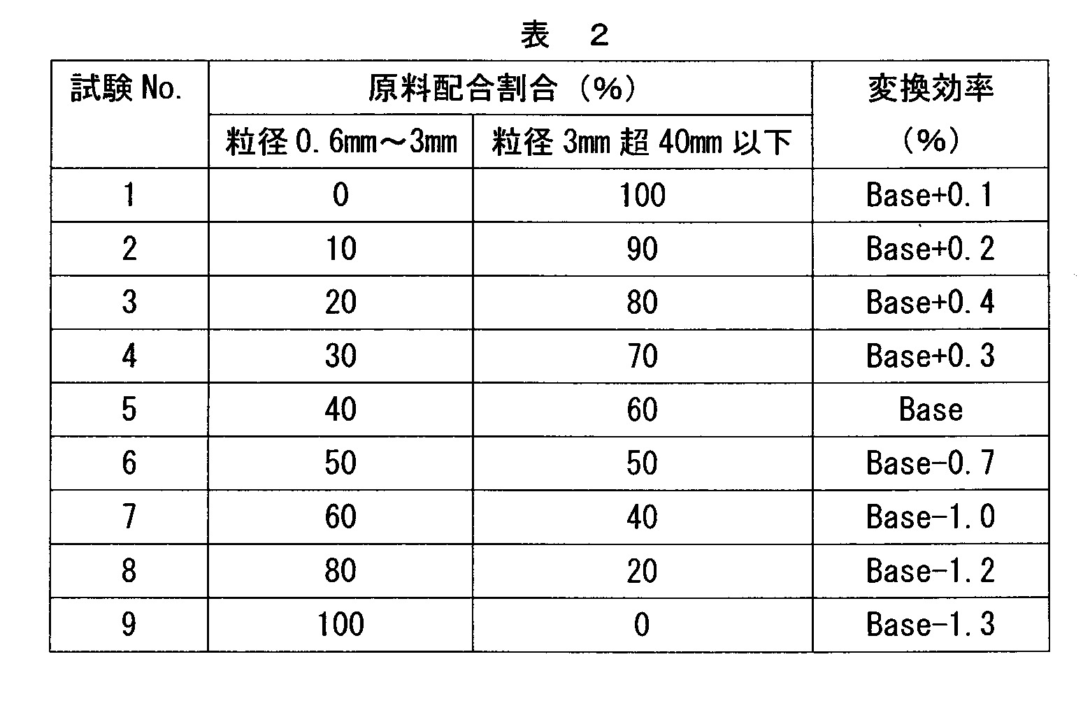
表2から明らかなように、粒径が3mmを超え40mm以下の原料を100%使用した場合は、粒径が0.6mm~3mmの原料の配合比率を40%以上と多くした場合(試験No.5~No.9)に比べて、変換効率が高かった。これは、原料の表面積が小さいため、原料投入前から原料表面に付着している金属不純物濃度が低かったことによるものと考えられる。一方、粒径が0.6mm~3mmの原料の配合比率が比較的小さい場合(試験No.2~No.4)に比べて変換効率が低かったのは、原料投入時に原料供給配管の内面に衝突した際の摩擦により金属汚染量が増加したことによるものと推察される。
粒径0.6mm~3mmの原料の割合を100%とした場合は、粒径が3mmを超え40mm以下の原料を比較的少なく配合した場合(試験No.6~No.8)に比べて変換効率が若干低下した。これは、原料供給配管の摩耗による金属汚染は減少したが、表面積が大きく、原料投入前から原料表面に付着している金属不純物濃度が高かったためと考えられる。
表2に示した結果から、良好な変換効率を得るためには、粒径範囲が0.6mm~3mmの原料の配合比率を0~40%、粒径範囲が3mmを超え40mm以下の原料の配合比率を100~60%とすることが必要であることがわかる。
粒径範囲が0.6mm~3mmの原料比率を20%とし、粒径範囲が3mmを超え40mm以下の原料比率を80%とした場合(試験No.3)、変換効率が最高値を示しており、金属汚染量が最も低いと考えられる。
本発明の多結晶シリコンの鋳造方法によれば、重金属による汚染が少なく、良好な変換効率を維持できる太陽電池の基板材としての多結晶シリコンを、簡素な構造で小型の原料供給配管を採用した電磁鋳造装置を使用して容易に製造することができる。したがって、本発明は、太陽電池の製造分野において有効に利用することができ、自然エネルギー利用技術の進展に大きく寄与することができる。
1:密閉容器、 2:加熱用誘導コイル、 3:板状片、 4:支持台、
5:保温装置(ヒータ)、 6:搬送機、 7:溶融シリコン、
8:鋳塊、 9:原料投入機、 10:発熱体
5:保温装置(ヒータ)、 6:搬送機、 7:溶融シリコン、
8:鋳塊、 9:原料投入機、 10:発熱体
Claims (2)
- 無底の冷却ルツボを用い、電磁誘導により多結晶シリコンを連続的に鋳造する多結晶シリコンの鋳造方法であって、
原料として、最大粒径が40mmであり、
かつ、粒径が0.6mm~3mmのものが0~40質量%、粒径が3mmを超え40mm以下のものが100~60質量%である高純度シリコンを使用することを特徴とする多結晶シリコンの鋳造方法。 - 原料として、粒径が0.6mm~3mmのものが20質量%、粒径が3mmを超え40mm以下のものが80質量%である高純度シリコンを使用することを特徴とする請求項1に記載の多結晶シリコンの鋳造方法。
Applications Claiming Priority (2)
| Application Number | Priority Date | Filing Date | Title |
|---|---|---|---|
| JP2010158593A JP2012020891A (ja) | 2010-07-13 | 2010-07-13 | 多結晶シリコンの鋳造方法 |
| JP2010-158593 | 2010-07-13 |
Publications (1)
| Publication Number | Publication Date |
|---|---|
| WO2012008003A1 true WO2012008003A1 (ja) | 2012-01-19 |
Family
ID=45469028
Family Applications (1)
| Application Number | Title | Priority Date | Filing Date |
|---|---|---|---|
| PCT/JP2010/006919 Ceased WO2012008003A1 (ja) | 2010-07-13 | 2010-11-26 | 多結晶シリコンの鋳造方法 |
Country Status (3)
| Country | Link |
|---|---|
| JP (1) | JP2012020891A (ja) |
| TW (1) | TW201202495A (ja) |
| WO (1) | WO2012008003A1 (ja) |
Citations (5)
| Publication number | Priority date | Publication date | Assignee | Title |
|---|---|---|---|---|
| JPH10182131A (ja) * | 1996-12-26 | 1998-07-07 | Kawasaki Steel Corp | シリコンの溶解方法 |
| JPH11314911A (ja) * | 1998-05-07 | 1999-11-16 | Sumitomo Sitix Amagasaki:Kk | 多結晶シリコンインゴットの製造方法 |
| JP2004149342A (ja) * | 2002-10-29 | 2004-05-27 | Kyocera Corp | シリコンの鋳造方法 |
| JP2008174397A (ja) * | 2007-01-16 | 2008-07-31 | Sumco Solar Corp | 多結晶シリコンの鋳造方法 |
| JP2009234850A (ja) * | 2008-03-27 | 2009-10-15 | Kyocera Corp | 結晶シリコン粒子の製造方法及び結晶シリコン粒子の製造装置 |
-
2010
- 2010-07-13 JP JP2010158593A patent/JP2012020891A/ja active Pending
- 2010-11-26 WO PCT/JP2010/006919 patent/WO2012008003A1/ja not_active Ceased
- 2010-12-01 TW TW99141782A patent/TW201202495A/zh unknown
Patent Citations (5)
| Publication number | Priority date | Publication date | Assignee | Title |
|---|---|---|---|---|
| JPH10182131A (ja) * | 1996-12-26 | 1998-07-07 | Kawasaki Steel Corp | シリコンの溶解方法 |
| JPH11314911A (ja) * | 1998-05-07 | 1999-11-16 | Sumitomo Sitix Amagasaki:Kk | 多結晶シリコンインゴットの製造方法 |
| JP2004149342A (ja) * | 2002-10-29 | 2004-05-27 | Kyocera Corp | シリコンの鋳造方法 |
| JP2008174397A (ja) * | 2007-01-16 | 2008-07-31 | Sumco Solar Corp | 多結晶シリコンの鋳造方法 |
| JP2009234850A (ja) * | 2008-03-27 | 2009-10-15 | Kyocera Corp | 結晶シリコン粒子の製造方法及び結晶シリコン粒子の製造装置 |
Also Published As
| Publication number | Publication date |
|---|---|
| TW201202495A (en) | 2012-01-16 |
| JP2012020891A (ja) | 2012-02-02 |
Similar Documents
| Publication | Publication Date | Title |
|---|---|---|
| JP5141020B2 (ja) | 多結晶シリコンの鋳造方法 | |
| JP5040521B2 (ja) | シリコン鋳造装置 | |
| US8501140B2 (en) | Method and apparatus for purifying metallurgical silicon for solar cells | |
| JP2008156166A (ja) | シリコンインゴットの鋳造方法および切断方法 | |
| US8845805B2 (en) | Device and method for producing crystalline bodies by directional solidification | |
| WO2012020462A1 (ja) | シリコンの電磁鋳造装置 | |
| JP2001019594A (ja) | シリコン連続鋳造方法 | |
| JP2657240B2 (ja) | シリコン鋳造装置 | |
| CN102120578A (zh) | 一种电子束除磷、除金属的耦合提纯多晶硅的方法及设备 | |
| US20070006916A1 (en) | Solar-cell polycrystalline silicon and method for producing the same | |
| Lee et al. | Directional solidification behaviors of polycrystalline silicon by electron-beam melting | |
| CN103903952B (zh) | 等离子蚀刻装置用硅部件及其制造方法 | |
| WO2012008003A1 (ja) | 多結晶シリコンの鋳造方法 | |
| JP2012136410A (ja) | 多結晶シリコンの鋳造方法 | |
| TW201341602A (zh) | 多晶矽及其鑄造方法 | |
| CN110396719A (zh) | 一种提高硅锭少子寿命的方法 | |
| JP2010254534A (ja) | 坩堝、該坩堝を用いた精製装置および精製方法 | |
| JP2883910B2 (ja) | 単結晶シリコンの製造方法 | |
| CN1956921A (zh) | 熔融硅的冷却块状物及其制造方法 | |
| KR20120031421A (ko) | 실리콘 잉곳의 전자 주조 방법 | |
| CN102471868A (zh) | 薄膜制造方法及能够用于其方法的硅材料 | |
| JP2012035320A (ja) | シリコンインゴットの連続鋳造装置および連続鋳造方法 | |
| JP2012025599A (ja) | シリコンインゴットの連続鋳造方法 | |
| JP2013112539A (ja) | シリコンインゴットの連続鋳造方法 | |
| JP2025033437A (ja) | シリコンインゴット、および、シリコンインゴットの製造方法 |
Legal Events
| Date | Code | Title | Description |
|---|---|---|---|
| 121 | Ep: the epo has been informed by wipo that ep was designated in this application |
Ref document number: 10854687 Country of ref document: EP Kind code of ref document: A1 |
|
| NENP | Non-entry into the national phase |
Ref country code: DE |
|
| 122 | Ep: pct application non-entry in european phase |
Ref document number: 10854687 Country of ref document: EP Kind code of ref document: A1 |