WO2011158811A1 - Grille de connexion pour dispositif à semi-conducteurs optique, procédé pour fabriquer une grille de connexion pour dispositif à semi-conducteurs optique, et dispositif à semi-conducteurs optique. - Google Patents
Grille de connexion pour dispositif à semi-conducteurs optique, procédé pour fabriquer une grille de connexion pour dispositif à semi-conducteurs optique, et dispositif à semi-conducteurs optique. Download PDFInfo
- Publication number
- WO2011158811A1 WO2011158811A1 PCT/JP2011/063542 JP2011063542W WO2011158811A1 WO 2011158811 A1 WO2011158811 A1 WO 2011158811A1 JP 2011063542 W JP2011063542 W JP 2011063542W WO 2011158811 A1 WO2011158811 A1 WO 2011158811A1
- Authority
- WO
- WIPO (PCT)
- Prior art keywords
- optical semiconductor
- semiconductor device
- lead frame
- alloy
- silver
- Prior art date
Links
- 239000004065 semiconductor Substances 0.000 title claims abstract description 181
- 230000003287 optical effect Effects 0.000 title claims abstract description 172
- 238000000034 method Methods 0.000 title claims abstract description 86
- 238000004519 manufacturing process Methods 0.000 title claims abstract description 29
- 238000007747 plating Methods 0.000 claims abstract description 245
- 229910052751 metal Inorganic materials 0.000 claims abstract description 82
- 239000002184 metal Substances 0.000 claims abstract description 82
- 239000000956 alloy Substances 0.000 claims abstract description 54
- 229910045601 alloy Inorganic materials 0.000 claims abstract description 52
- 238000005096 rolling process Methods 0.000 claims description 122
- 229910052709 silver Inorganic materials 0.000 claims description 106
- 238000012545 processing Methods 0.000 claims description 105
- BQCADISMDOOEFD-UHFFFAOYSA-N Silver Chemical compound [Ag] BQCADISMDOOEFD-UHFFFAOYSA-N 0.000 claims description 102
- 239000004332 silver Substances 0.000 claims description 102
- 230000003746 surface roughness Effects 0.000 claims description 102
- 239000000758 substrate Substances 0.000 claims description 83
- 239000000463 material Substances 0.000 claims description 59
- 229910001316 Ag alloy Inorganic materials 0.000 claims description 43
- 238000005498 polishing Methods 0.000 claims description 31
- 238000003825 pressing Methods 0.000 claims description 26
- 239000010949 copper Substances 0.000 claims description 25
- 229910052802 copper Inorganic materials 0.000 claims description 21
- 239000010931 gold Substances 0.000 claims description 21
- RYGMFSIKBFXOCR-UHFFFAOYSA-N Copper Chemical compound [Cu] RYGMFSIKBFXOCR-UHFFFAOYSA-N 0.000 claims description 19
- XEEYBQQBJWHFJM-UHFFFAOYSA-N Iron Chemical compound [Fe] XEEYBQQBJWHFJM-UHFFFAOYSA-N 0.000 claims description 16
- 229910052737 gold Inorganic materials 0.000 claims description 16
- 238000005476 soldering Methods 0.000 claims description 13
- PCHJSUWPFVWCPO-UHFFFAOYSA-N gold Chemical compound [Au] PCHJSUWPFVWCPO-UHFFFAOYSA-N 0.000 claims description 12
- BASFCYQUMIYNBI-UHFFFAOYSA-N platinum Chemical compound [Pt] BASFCYQUMIYNBI-UHFFFAOYSA-N 0.000 claims description 12
- 230000008569 process Effects 0.000 claims description 12
- 229910052782 aluminium Inorganic materials 0.000 claims description 11
- 229910052718 tin Inorganic materials 0.000 claims description 11
- 229910000881 Cu alloy Inorganic materials 0.000 claims description 10
- 229910001128 Sn alloy Inorganic materials 0.000 claims description 10
- XAGFODPZIPBFFR-UHFFFAOYSA-N aluminium Chemical compound [Al] XAGFODPZIPBFFR-UHFFFAOYSA-N 0.000 claims description 10
- 238000005530 etching Methods 0.000 claims description 10
- 229910001020 Au alloy Inorganic materials 0.000 claims description 9
- 239000003353 gold alloy Substances 0.000 claims description 9
- ATJFFYVFTNAWJD-UHFFFAOYSA-N Tin Chemical compound [Sn] ATJFFYVFTNAWJD-UHFFFAOYSA-N 0.000 claims description 8
- 229910052742 iron Inorganic materials 0.000 claims description 8
- 238000005286 illumination Methods 0.000 claims description 7
- 239000010948 rhodium Substances 0.000 claims description 7
- 229910000846 In alloy Inorganic materials 0.000 claims description 6
- 229910001245 Sb alloy Inorganic materials 0.000 claims description 6
- 229910001370 Se alloy Inorganic materials 0.000 claims description 6
- 229910001252 Pd alloy Inorganic materials 0.000 claims description 5
- QCEUXSAXTBNJGO-UHFFFAOYSA-N [Ag].[Sn] Chemical compound [Ag].[Sn] QCEUXSAXTBNJGO-UHFFFAOYSA-N 0.000 claims description 5
- 239000002140 antimony alloy Substances 0.000 claims description 5
- LGFYIAWZICUNLK-UHFFFAOYSA-N antimony silver Chemical compound [Ag].[Sb] LGFYIAWZICUNLK-UHFFFAOYSA-N 0.000 claims description 5
- YZASAXHKAQYPEH-UHFFFAOYSA-N indium silver Chemical compound [Ag].[In] YZASAXHKAQYPEH-UHFFFAOYSA-N 0.000 claims description 5
- 229910052697 platinum Inorganic materials 0.000 claims description 5
- 238000004080 punching Methods 0.000 claims description 5
- 229910000838 Al alloy Inorganic materials 0.000 claims description 4
- 229910000990 Ni alloy Inorganic materials 0.000 claims description 4
- PQTCMBYFWMFIGM-UHFFFAOYSA-N gold silver Chemical compound [Ag].[Au] PQTCMBYFWMFIGM-UHFFFAOYSA-N 0.000 claims description 4
- SWELZOZIOHGSPA-UHFFFAOYSA-N palladium silver Chemical compound [Pd].[Ag] SWELZOZIOHGSPA-UHFFFAOYSA-N 0.000 claims description 4
- 229910052703 rhodium Inorganic materials 0.000 claims description 4
- 229910000640 Fe alloy Inorganic materials 0.000 claims description 3
- 229910001260 Pt alloy Inorganic materials 0.000 claims description 3
- 229910000629 Rh alloy Inorganic materials 0.000 claims description 3
- 229910000929 Ru alloy Inorganic materials 0.000 claims description 3
- IHWJXGQYRBHUIF-UHFFFAOYSA-N [Ag].[Pt] Chemical compound [Ag].[Pt] IHWJXGQYRBHUIF-UHFFFAOYSA-N 0.000 claims description 3
- IOBIJTFWSZQXPN-UHFFFAOYSA-N [Rh].[Ag] Chemical compound [Rh].[Ag] IOBIJTFWSZQXPN-UHFFFAOYSA-N 0.000 claims description 3
- JMGVPAUIBBRNCO-UHFFFAOYSA-N [Ru].[Ag] Chemical compound [Ru].[Ag] JMGVPAUIBBRNCO-UHFFFAOYSA-N 0.000 claims description 3
- MOFOBJHOKRNACT-UHFFFAOYSA-N nickel silver Chemical compound [Ni].[Ag] MOFOBJHOKRNACT-UHFFFAOYSA-N 0.000 claims description 3
- MHOVAHRLVXNVSD-UHFFFAOYSA-N rhodium atom Chemical compound [Rh] MHOVAHRLVXNVSD-UHFFFAOYSA-N 0.000 claims description 3
- BUGBHKTXTAQXES-UHFFFAOYSA-N Selenium Chemical class [Se] BUGBHKTXTAQXES-UHFFFAOYSA-N 0.000 claims 1
- 239000010410 layer Substances 0.000 description 154
- 239000011347 resin Substances 0.000 description 42
- 229920005989 resin Polymers 0.000 description 42
- 238000010438 heat treatment Methods 0.000 description 41
- 238000002310 reflectometry Methods 0.000 description 36
- 239000013078 crystal Substances 0.000 description 26
- 238000009713 electroplating Methods 0.000 description 24
- 239000004033 plastic Substances 0.000 description 23
- 230000006872 improvement Effects 0.000 description 20
- 239000010944 silver (metal) Substances 0.000 description 20
- 238000005259 measurement Methods 0.000 description 18
- 239000000047 product Substances 0.000 description 16
- 235000019592 roughness Nutrition 0.000 description 16
- HEMHJVSKTPXQMS-UHFFFAOYSA-M Sodium hydroxide Chemical compound [OH-].[Na+] HEMHJVSKTPXQMS-UHFFFAOYSA-M 0.000 description 15
- 230000009467 reduction Effects 0.000 description 14
- 238000007789 sealing Methods 0.000 description 14
- 229910000679 solder Inorganic materials 0.000 description 14
- 238000010521 absorption reaction Methods 0.000 description 12
- 230000002829 reductive effect Effects 0.000 description 12
- 239000003566 sealing material Substances 0.000 description 12
- 238000004544 sputter deposition Methods 0.000 description 12
- 238000000576 coating method Methods 0.000 description 11
- 230000000694 effects Effects 0.000 description 11
- 238000011156 evaluation Methods 0.000 description 11
- PXHVJJICTQNCMI-UHFFFAOYSA-N Nickel Chemical compound [Ni] PXHVJJICTQNCMI-UHFFFAOYSA-N 0.000 description 10
- 238000005452 bending Methods 0.000 description 10
- 239000011248 coating agent Substances 0.000 description 10
- 238000005238 degreasing Methods 0.000 description 10
- 239000011135 tin Substances 0.000 description 10
- 238000009736 wetting Methods 0.000 description 10
- VYPSYNLAJGMNEJ-UHFFFAOYSA-N Silicium dioxide Chemical compound O=[Si]=O VYPSYNLAJGMNEJ-UHFFFAOYSA-N 0.000 description 9
- 230000015572 biosynthetic process Effects 0.000 description 9
- 239000008119 colloidal silica Substances 0.000 description 9
- 238000007772 electroless plating Methods 0.000 description 9
- 230000007423 decrease Effects 0.000 description 8
- 230000006866 deterioration Effects 0.000 description 8
- 238000009499 grossing Methods 0.000 description 8
- 238000005554 pickling Methods 0.000 description 8
- OAICVXFJPJFONN-UHFFFAOYSA-N Phosphorus Chemical compound [P] OAICVXFJPJFONN-UHFFFAOYSA-N 0.000 description 6
- 230000008859 change Effects 0.000 description 6
- 238000007654 immersion Methods 0.000 description 6
- 238000012360 testing method Methods 0.000 description 6
- 238000000137 annealing Methods 0.000 description 5
- 238000009792 diffusion process Methods 0.000 description 5
- 238000005516 engineering process Methods 0.000 description 5
- FAPWRFPIFSIZLT-UHFFFAOYSA-M Sodium chloride Chemical compound [Na+].[Cl-] FAPWRFPIFSIZLT-UHFFFAOYSA-M 0.000 description 4
- QAOWNCQODCNURD-UHFFFAOYSA-N Sulfuric acid Chemical compound OS(O)(=O)=O QAOWNCQODCNURD-UHFFFAOYSA-N 0.000 description 4
- 238000005275 alloying Methods 0.000 description 4
- 238000005097 cold rolling Methods 0.000 description 4
- 230000000052 comparative effect Effects 0.000 description 4
- 238000002845 discoloration Methods 0.000 description 4
- 239000011521 glass Substances 0.000 description 4
- 230000017525 heat dissipation Effects 0.000 description 4
- 229910052759 nickel Inorganic materials 0.000 description 4
- 230000003647 oxidation Effects 0.000 description 4
- 238000007254 oxidation reaction Methods 0.000 description 4
- KRRRBSZQCHDZMP-UHFFFAOYSA-N selanylidenesilver Chemical compound [Ag]=[Se] KRRRBSZQCHDZMP-UHFFFAOYSA-N 0.000 description 4
- LFAGQMCIGQNPJG-UHFFFAOYSA-N silver cyanide Chemical compound [Ag+].N#[C-] LFAGQMCIGQNPJG-UHFFFAOYSA-N 0.000 description 4
- HCHKCACWOHOZIP-UHFFFAOYSA-N Zinc Chemical compound [Zn] HCHKCACWOHOZIP-UHFFFAOYSA-N 0.000 description 3
- 239000012298 atmosphere Substances 0.000 description 3
- 239000003795 chemical substances by application Substances 0.000 description 3
- 238000007796 conventional method Methods 0.000 description 3
- 230000007797 corrosion Effects 0.000 description 3
- 238000005260 corrosion Methods 0.000 description 3
- 230000003247 decreasing effect Effects 0.000 description 3
- 238000000151 deposition Methods 0.000 description 3
- 230000007613 environmental effect Effects 0.000 description 3
- 239000007789 gas Substances 0.000 description 3
- 150000002739 metals Chemical class 0.000 description 3
- KDLHZDBZIXYQEI-UHFFFAOYSA-N palladium Substances [Pd] KDLHZDBZIXYQEI-UHFFFAOYSA-N 0.000 description 3
- 238000009877 rendering Methods 0.000 description 3
- 229920006395 saturated elastomer Polymers 0.000 description 3
- 229910052725 zinc Inorganic materials 0.000 description 3
- 239000011701 zinc Substances 0.000 description 3
- 229910000531 Co alloy Inorganic materials 0.000 description 2
- 239000006061 abrasive grain Substances 0.000 description 2
- QVGXLLKOCUKJST-UHFFFAOYSA-N atomic oxygen Chemical compound [O] QVGXLLKOCUKJST-UHFFFAOYSA-N 0.000 description 2
- TZCXTZWJZNENPQ-UHFFFAOYSA-L barium sulfate Chemical compound [Ba+2].[O-]S([O-])(=O)=O TZCXTZWJZNENPQ-UHFFFAOYSA-L 0.000 description 2
- 230000008901 benefit Effects 0.000 description 2
- 230000008033 biological extinction Effects 0.000 description 2
- 239000000919 ceramic Substances 0.000 description 2
- 239000010941 cobalt Substances 0.000 description 2
- 229910017052 cobalt Inorganic materials 0.000 description 2
- GUTLYIVDDKVIGB-UHFFFAOYSA-N cobalt atom Chemical compound [Co] GUTLYIVDDKVIGB-UHFFFAOYSA-N 0.000 description 2
- 230000001276 controlling effect Effects 0.000 description 2
- 230000020169 heat generation Effects 0.000 description 2
- 239000007788 liquid Substances 0.000 description 2
- 230000007774 longterm Effects 0.000 description 2
- 238000010297 mechanical methods and process Methods 0.000 description 2
- 230000005226 mechanical processes and functions Effects 0.000 description 2
- 239000007769 metal material Substances 0.000 description 2
- 239000000203 mixture Substances 0.000 description 2
- 238000000465 moulding Methods 0.000 description 2
- 229910052760 oxygen Inorganic materials 0.000 description 2
- 239000001301 oxygen Substances 0.000 description 2
- 230000036961 partial effect Effects 0.000 description 2
- 239000002245 particle Substances 0.000 description 2
- 239000012466 permeate Substances 0.000 description 2
- 238000011160 research Methods 0.000 description 2
- 239000011780 sodium chloride Substances 0.000 description 2
- 239000012798 spherical particle Substances 0.000 description 2
- 239000002344 surface layer Substances 0.000 description 2
- 239000000725 suspension Substances 0.000 description 2
- 238000005496 tempering Methods 0.000 description 2
- RSWGJHLUYNHPMX-UHFFFAOYSA-N Abietic-Saeure Natural products C12CCC(C(C)C)=CC2=CCC2C1(C)CCCC2(C)C(O)=O RSWGJHLUYNHPMX-UHFFFAOYSA-N 0.000 description 1
- 229910017980 Ag—Sn Inorganic materials 0.000 description 1
- 102100024222 B-lymphocyte antigen CD19 Human genes 0.000 description 1
- 229910001369 Brass Inorganic materials 0.000 description 1
- 229910000906 Bronze Inorganic materials 0.000 description 1
- 229910017827 Cu—Fe Inorganic materials 0.000 description 1
- 101000980825 Homo sapiens B-lymphocyte antigen CD19 Proteins 0.000 description 1
- 229910021617 Indium monochloride Inorganic materials 0.000 description 1
- 241001464887 Parvimonas micra Species 0.000 description 1
- 101150003085 Pdcl gene Proteins 0.000 description 1
- KHPCPRHQVVSZAH-HUOMCSJISA-N Rosin Natural products O(C/C=C/c1ccccc1)[C@H]1[C@H](O)[C@@H](O)[C@@H](O)[C@@H](CO)O1 KHPCPRHQVVSZAH-HUOMCSJISA-N 0.000 description 1
- NINIDFKCEFEMDL-UHFFFAOYSA-N Sulfur Chemical compound [S] NINIDFKCEFEMDL-UHFFFAOYSA-N 0.000 description 1
- FEWJPZIEWOKRBE-UHFFFAOYSA-N Tartaric acid Natural products [H+].[H+].[O-]C(=O)C(O)C(O)C([O-])=O FEWJPZIEWOKRBE-UHFFFAOYSA-N 0.000 description 1
- 239000002390 adhesive tape Substances 0.000 description 1
- 230000032683 aging Effects 0.000 description 1
- 230000004075 alteration Effects 0.000 description 1
- PNEYBMLMFCGWSK-UHFFFAOYSA-N aluminium oxide Inorganic materials [O-2].[O-2].[O-2].[Al+3].[Al+3] PNEYBMLMFCGWSK-UHFFFAOYSA-N 0.000 description 1
- 239000010951 brass Substances 0.000 description 1
- 239000010974 bronze Substances 0.000 description 1
- 238000005253 cladding Methods 0.000 description 1
- 239000011247 coating layer Substances 0.000 description 1
- 239000003086 colorant Substances 0.000 description 1
- 239000004020 conductor Substances 0.000 description 1
- 239000000470 constituent Substances 0.000 description 1
- KUNSUQLRTQLHQQ-UHFFFAOYSA-N copper tin Chemical compound [Cu].[Sn] KUNSUQLRTQLHQQ-UHFFFAOYSA-N 0.000 description 1
- 230000003111 delayed effect Effects 0.000 description 1
- 238000011161 development Methods 0.000 description 1
- 230000018109 developmental process Effects 0.000 description 1
- 238000004070 electrodeposition Methods 0.000 description 1
- 230000003628 erosive effect Effects 0.000 description 1
- 238000002474 experimental method Methods 0.000 description 1
- 239000010419 fine particle Substances 0.000 description 1
- 238000007667 floating Methods 0.000 description 1
- 239000012535 impurity Substances 0.000 description 1
- APHGZSBLRQFRCA-UHFFFAOYSA-M indium(1+);chloride Chemical compound [In]Cl APHGZSBLRQFRCA-UHFFFAOYSA-M 0.000 description 1
- 239000011229 interlayer Substances 0.000 description 1
- 125000001449 isopropyl group Chemical group [H]C([H])([H])C([H])(*)C([H])([H])[H] 0.000 description 1
- 230000031700 light absorption Effects 0.000 description 1
- 230000000670 limiting effect Effects 0.000 description 1
- 238000003754 machining Methods 0.000 description 1
- 238000000691 measurement method Methods 0.000 description 1
- 230000004048 modification Effects 0.000 description 1
- 238000012986 modification Methods 0.000 description 1
- 239000012299 nitrogen atmosphere Substances 0.000 description 1
- 229910000510 noble metal Inorganic materials 0.000 description 1
- 230000006911 nucleation Effects 0.000 description 1
- 238000010899 nucleation Methods 0.000 description 1
- 238000001579 optical reflectometry Methods 0.000 description 1
- TWNQGVIAIRXVLR-UHFFFAOYSA-N oxo(oxoalumanyloxy)alumane Chemical compound O=[Al]O[Al]=O TWNQGVIAIRXVLR-UHFFFAOYSA-N 0.000 description 1
- 229910052763 palladium Inorganic materials 0.000 description 1
- 230000002093 peripheral effect Effects 0.000 description 1
- 230000035699 permeability Effects 0.000 description 1
- 230000001699 photocatalysis Effects 0.000 description 1
- 229920006267 polyester film Polymers 0.000 description 1
- ZNNZYHKDIALBAK-UHFFFAOYSA-M potassium thiocyanate Chemical compound [K+].[S-]C#N ZNNZYHKDIALBAK-UHFFFAOYSA-M 0.000 description 1
- 239000010970 precious metal Substances 0.000 description 1
- 230000001376 precipitating effect Effects 0.000 description 1
- 238000001556 precipitation Methods 0.000 description 1
- 230000002250 progressing effect Effects 0.000 description 1
- 230000002035 prolonged effect Effects 0.000 description 1
- 239000012925 reference material Substances 0.000 description 1
- 230000001105 regulatory effect Effects 0.000 description 1
- 230000001846 repelling effect Effects 0.000 description 1
- 230000004044 response Effects 0.000 description 1
- 230000000630 rising effect Effects 0.000 description 1
- 229910052710 silicon Inorganic materials 0.000 description 1
- 239000010703 silicon Substances 0.000 description 1
- 238000005477 sputtering target Methods 0.000 description 1
- 238000003860 storage Methods 0.000 description 1
- 239000000126 substance Substances 0.000 description 1
- 238000006467 substitution reaction Methods 0.000 description 1
- 229910052717 sulfur Inorganic materials 0.000 description 1
- 239000011593 sulfur Substances 0.000 description 1
- 235000002906 tartaric acid Nutrition 0.000 description 1
- 239000011975 tartaric acid Substances 0.000 description 1
- KHPCPRHQVVSZAH-UHFFFAOYSA-N trans-cinnamyl beta-D-glucopyranoside Natural products OC1C(O)C(O)C(CO)OC1OCC=CC1=CC=CC=C1 KHPCPRHQVVSZAH-UHFFFAOYSA-N 0.000 description 1
Images


Classifications
-
- H—ELECTRICITY
- H01—ELECTRIC ELEMENTS
- H01L—SEMICONDUCTOR DEVICES NOT COVERED BY CLASS H10
- H01L33/00—Semiconductor devices having potential barriers specially adapted for light emission; Processes or apparatus specially adapted for the manufacture or treatment thereof or of parts thereof; Details thereof
- H01L33/48—Semiconductor devices having potential barriers specially adapted for light emission; Processes or apparatus specially adapted for the manufacture or treatment thereof or of parts thereof; Details thereof characterised by the semiconductor body packages
- H01L33/62—Arrangements for conducting electric current to or from the semiconductor body, e.g. lead-frames, wire-bonds or solder balls
-
- H—ELECTRICITY
- H01—ELECTRIC ELEMENTS
- H01L—SEMICONDUCTOR DEVICES NOT COVERED BY CLASS H10
- H01L33/00—Semiconductor devices having potential barriers specially adapted for light emission; Processes or apparatus specially adapted for the manufacture or treatment thereof or of parts thereof; Details thereof
- H01L33/48—Semiconductor devices having potential barriers specially adapted for light emission; Processes or apparatus specially adapted for the manufacture or treatment thereof or of parts thereof; Details thereof characterised by the semiconductor body packages
- H01L33/58—Optical field-shaping elements
- H01L33/60—Reflective elements
-
- C—CHEMISTRY; METALLURGY
- C25—ELECTROLYTIC OR ELECTROPHORETIC PROCESSES; APPARATUS THEREFOR
- C25D—PROCESSES FOR THE ELECTROLYTIC OR ELECTROPHORETIC PRODUCTION OF COATINGS; ELECTROFORMING; APPARATUS THEREFOR
- C25D5/00—Electroplating characterised by the process; Pretreatment or after-treatment of workpieces
- C25D5/10—Electroplating with more than one layer of the same or of different metals
- C25D5/12—Electroplating with more than one layer of the same or of different metals at least one layer being of nickel or chromium
-
- C—CHEMISTRY; METALLURGY
- C25—ELECTROLYTIC OR ELECTROPHORETIC PROCESSES; APPARATUS THEREFOR
- C25D—PROCESSES FOR THE ELECTROLYTIC OR ELECTROPHORETIC PRODUCTION OF COATINGS; ELECTROFORMING; APPARATUS THEREFOR
- C25D5/00—Electroplating characterised by the process; Pretreatment or after-treatment of workpieces
- C25D5/48—After-treatment of electroplated surfaces
-
- C—CHEMISTRY; METALLURGY
- C25—ELECTROLYTIC OR ELECTROPHORETIC PROCESSES; APPARATUS THEREFOR
- C25D—PROCESSES FOR THE ELECTROLYTIC OR ELECTROPHORETIC PRODUCTION OF COATINGS; ELECTROFORMING; APPARATUS THEREFOR
- C25D5/00—Electroplating characterised by the process; Pretreatment or after-treatment of workpieces
- C25D5/60—Electroplating characterised by the structure or texture of the layers
- C25D5/605—Surface topography of the layers, e.g. rough, dendritic or nodular layers
- C25D5/611—Smooth layers
-
- C—CHEMISTRY; METALLURGY
- C25—ELECTROLYTIC OR ELECTROPHORETIC PROCESSES; APPARATUS THEREFOR
- C25D—PROCESSES FOR THE ELECTROLYTIC OR ELECTROPHORETIC PRODUCTION OF COATINGS; ELECTROFORMING; APPARATUS THEREFOR
- C25D5/00—Electroplating characterised by the process; Pretreatment or after-treatment of workpieces
- C25D5/60—Electroplating characterised by the structure or texture of the layers
- C25D5/615—Microstructure of the layers, e.g. mixed structure
- C25D5/617—Crystalline layers
-
- C—CHEMISTRY; METALLURGY
- C25—ELECTROLYTIC OR ELECTROPHORETIC PROCESSES; APPARATUS THEREFOR
- C25D—PROCESSES FOR THE ELECTROLYTIC OR ELECTROPHORETIC PRODUCTION OF COATINGS; ELECTROFORMING; APPARATUS THEREFOR
- C25D5/00—Electroplating characterised by the process; Pretreatment or after-treatment of workpieces
- C25D5/627—Electroplating characterised by the visual appearance of the layers, e.g. colour, brightness or mat appearance
-
- C—CHEMISTRY; METALLURGY
- C25—ELECTROLYTIC OR ELECTROPHORETIC PROCESSES; APPARATUS THEREFOR
- C25D—PROCESSES FOR THE ELECTROLYTIC OR ELECTROPHORETIC PRODUCTION OF COATINGS; ELECTROFORMING; APPARATUS THEREFOR
- C25D7/00—Electroplating characterised by the article coated
- C25D7/08—Mirrors; Reflectors
-
- H—ELECTRICITY
- H01—ELECTRIC ELEMENTS
- H01L—SEMICONDUCTOR DEVICES NOT COVERED BY CLASS H10
- H01L23/00—Details of semiconductor or other solid state devices
- H01L23/48—Arrangements for conducting electric current to or from the solid state body in operation, e.g. leads, terminal arrangements ; Selection of materials therefor
- H01L23/488—Arrangements for conducting electric current to or from the solid state body in operation, e.g. leads, terminal arrangements ; Selection of materials therefor consisting of soldered or bonded constructions
- H01L23/495—Lead-frames or other flat leads
- H01L23/49534—Multi-layer
-
- H—ELECTRICITY
- H01—ELECTRIC ELEMENTS
- H01L—SEMICONDUCTOR DEVICES NOT COVERED BY CLASS H10
- H01L23/00—Details of semiconductor or other solid state devices
- H01L23/48—Arrangements for conducting electric current to or from the solid state body in operation, e.g. leads, terminal arrangements ; Selection of materials therefor
- H01L23/488—Arrangements for conducting electric current to or from the solid state body in operation, e.g. leads, terminal arrangements ; Selection of materials therefor consisting of soldered or bonded constructions
- H01L23/495—Lead-frames or other flat leads
- H01L23/49579—Lead-frames or other flat leads characterised by the materials of the lead frames or layers thereon
-
- C—CHEMISTRY; METALLURGY
- C25—ELECTROLYTIC OR ELECTROPHORETIC PROCESSES; APPARATUS THEREFOR
- C25D—PROCESSES FOR THE ELECTROLYTIC OR ELECTROPHORETIC PRODUCTION OF COATINGS; ELECTROFORMING; APPARATUS THEREFOR
- C25D3/00—Electroplating: Baths therefor
- C25D3/02—Electroplating: Baths therefor from solutions
- C25D3/12—Electroplating: Baths therefor from solutions of nickel or cobalt
-
- C—CHEMISTRY; METALLURGY
- C25—ELECTROLYTIC OR ELECTROPHORETIC PROCESSES; APPARATUS THEREFOR
- C25D—PROCESSES FOR THE ELECTROLYTIC OR ELECTROPHORETIC PRODUCTION OF COATINGS; ELECTROFORMING; APPARATUS THEREFOR
- C25D3/00—Electroplating: Baths therefor
- C25D3/02—Electroplating: Baths therefor from solutions
- C25D3/38—Electroplating: Baths therefor from solutions of copper
-
- C—CHEMISTRY; METALLURGY
- C25—ELECTROLYTIC OR ELECTROPHORETIC PROCESSES; APPARATUS THEREFOR
- C25D—PROCESSES FOR THE ELECTROLYTIC OR ELECTROPHORETIC PRODUCTION OF COATINGS; ELECTROFORMING; APPARATUS THEREFOR
- C25D3/00—Electroplating: Baths therefor
- C25D3/02—Electroplating: Baths therefor from solutions
- C25D3/46—Electroplating: Baths therefor from solutions of silver
-
- C—CHEMISTRY; METALLURGY
- C25—ELECTROLYTIC OR ELECTROPHORETIC PROCESSES; APPARATUS THEREFOR
- C25D—PROCESSES FOR THE ELECTROLYTIC OR ELECTROPHORETIC PRODUCTION OF COATINGS; ELECTROFORMING; APPARATUS THEREFOR
- C25D3/00—Electroplating: Baths therefor
- C25D3/02—Electroplating: Baths therefor from solutions
- C25D3/56—Electroplating: Baths therefor from solutions of alloys
- C25D3/64—Electroplating: Baths therefor from solutions of alloys containing more than 50% by weight of silver
-
- C—CHEMISTRY; METALLURGY
- C25—ELECTROLYTIC OR ELECTROPHORETIC PROCESSES; APPARATUS THEREFOR
- C25D—PROCESSES FOR THE ELECTROLYTIC OR ELECTROPHORETIC PRODUCTION OF COATINGS; ELECTROFORMING; APPARATUS THEREFOR
- C25D5/00—Electroplating characterised by the process; Pretreatment or after-treatment of workpieces
- C25D5/02—Electroplating of selected surface areas
- C25D5/022—Electroplating of selected surface areas using masking means
-
- C—CHEMISTRY; METALLURGY
- C25—ELECTROLYTIC OR ELECTROPHORETIC PROCESSES; APPARATUS THEREFOR
- C25D—PROCESSES FOR THE ELECTROLYTIC OR ELECTROPHORETIC PRODUCTION OF COATINGS; ELECTROFORMING; APPARATUS THEREFOR
- C25D5/00—Electroplating characterised by the process; Pretreatment or after-treatment of workpieces
- C25D5/34—Pretreatment of metallic surfaces to be electroplated
- C25D5/36—Pretreatment of metallic surfaces to be electroplated of iron or steel
-
- C—CHEMISTRY; METALLURGY
- C25—ELECTROLYTIC OR ELECTROPHORETIC PROCESSES; APPARATUS THEREFOR
- C25D—PROCESSES FOR THE ELECTROLYTIC OR ELECTROPHORETIC PRODUCTION OF COATINGS; ELECTROFORMING; APPARATUS THEREFOR
- C25D5/00—Electroplating characterised by the process; Pretreatment or after-treatment of workpieces
- C25D5/34—Pretreatment of metallic surfaces to be electroplated
- C25D5/42—Pretreatment of metallic surfaces to be electroplated of light metals
- C25D5/44—Aluminium
-
- C—CHEMISTRY; METALLURGY
- C25—ELECTROLYTIC OR ELECTROPHORETIC PROCESSES; APPARATUS THEREFOR
- C25D—PROCESSES FOR THE ELECTROLYTIC OR ELECTROPHORETIC PRODUCTION OF COATINGS; ELECTROFORMING; APPARATUS THEREFOR
- C25D5/00—Electroplating characterised by the process; Pretreatment or after-treatment of workpieces
- C25D5/48—After-treatment of electroplated surfaces
- C25D5/50—After-treatment of electroplated surfaces by heat-treatment
-
- H—ELECTRICITY
- H01—ELECTRIC ELEMENTS
- H01L—SEMICONDUCTOR DEVICES NOT COVERED BY CLASS H10
- H01L2924/00—Indexing scheme for arrangements or methods for connecting or disconnecting semiconductor or solid-state bodies as covered by H01L24/00
- H01L2924/0001—Technical content checked by a classifier
- H01L2924/0002—Not covered by any one of groups H01L24/00, H01L24/00 and H01L2224/00
-
- H—ELECTRICITY
- H01—ELECTRIC ELEMENTS
- H01L—SEMICONDUCTOR DEVICES NOT COVERED BY CLASS H10
- H01L33/00—Semiconductor devices having potential barriers specially adapted for light emission; Processes or apparatus specially adapted for the manufacture or treatment thereof or of parts thereof; Details thereof
- H01L33/48—Semiconductor devices having potential barriers specially adapted for light emission; Processes or apparatus specially adapted for the manufacture or treatment thereof or of parts thereof; Details thereof characterised by the semiconductor body packages
- H01L33/483—Containers
- H01L33/486—Containers adapted for surface mounting
Definitions
- the present invention relates to an optical semiconductor device lead frame, a manufacturing method thereof, and an optical semiconductor device.
- the reflective material of the lead frame has a high reflectance in the entire visible light wavelength range (400 to 800 nm) (for example, the reflectance with respect to a reference material such as barium sulfate or aluminum oxide). 80% or more).
- the use of LEDs that emit ultraviolet rays has been expanded, such as light sources for measuring / analyzing instruments that use ultraviolet rays, photocatalytic air purifiers, ultraviolet sensors, and light sources for curing ultraviolet curable resins.
- optical semiconductor devices using LED elements have come to be used.
- a layer (film) made of silver or a silver alloy is formed on the lead frame on which the LED element is mounted, particularly for the purpose of improving the light reflectance in the visible light region (hereinafter referred to as reflectance). ) Is often formed.
- the silver film has a high reflectance in the visible light region.
- a silver plating layer is formed on the reflection surface (Patent Document 1), or 200 or after the silver or silver alloy film is formed. It is known that a heat treatment is performed at a temperature of not lower than 30 ° C. for 30 seconds or longer, and the crystal grain size of the film is 0.5 ⁇ m to 30 ⁇ m (Patent Document 2).
- the absorption peak in the near ultraviolet region also affects the reflectance in the visible light region (near 400 nm to 800 nm). It has also led to a decline. This problem is particularly apparent at wavelengths near the near ultraviolet region.
- the luminous efficiency of the LED is improved year by year, it is still about 20%, so that the reflectance is low by 10% means a significant reduction in luminance. For this reason, when using a chip having a wavelength of 340 to 400 nm, which is in the near ultraviolet region, it is necessary to improve the reflectance in this wavelength region. By improving the reflectance of the lead frame material, it is possible to improve the luminance around one LED.
- Patent Document 3 has no knowledge about optical characteristics such as reflectance, and is not a rolling process for the purpose of improving reflectance.
- low-temperature annealing heat treatment
- the substrate component diffused to the surface layer due to the heating and lowered the reflectivity.
- the contact surface is maintained because the new surface is exposed by sliding and good conduction is obtained.
- the state of the outermost surface contributes most to the optical reflection phenomenon, so that the reflectivity is considered to decrease. From this, it can be seen that simply by rolling after plating and annealing, it cannot be easily developed for an optical semiconductor lead frame.
- the luminous efficiency of the LED module is affected by the reflectance of the lead frame surface as well as the luminous efficiency of the LED chip. If the reflectivity of the lead frame surface is low, not only the light emission efficiency of the LED module is lowered, but also the heat generation on the lead frame surface is increased and the sealing resin is deteriorated. . For this reason, when an LED module having high color rendering properties using an LED chip that emits ultraviolet light is to be realized, there is a strong demand for improving the reflectivity of the lead frame in the near ultraviolet region with a wavelength of 340 to 400 nm.
- the emission wavelength of the optical semiconductor chip mounted on the white LED module is still mainly around 450 nm.
- the improvement in the reflectance in the visible light region is very effective in improving the luminance of the LED module, and it is required to be as close as possible to the theoretical reflectance of the silver film (the reflectance is about 98% at 450 nm).
- the reflectance is about 98% at 450 nm.
- even in the case of a film made of a metal other than silver or an alloy thereof it has been required to achieve a high reflectance in the near ultraviolet region to the visible light region, which is required as an optical semiconductor lead frame.
- the present invention provides a lead frame for an optical semiconductor device used in LEDs, photocouplers, photointerrupters, and the like that include a near-ultraviolet to visible light range (wavelength 340 to 800 nm) in the emission wavelength. 400nm), particularly in the vicinity of a wavelength of 375nm and in the visible light region (wavelength of 400 to 800nm), particularly in the case of mounting a chip that emits light in the vicinity of a wavelength of 450nm.
- the task is to do.
- Another object is to provide an optical semiconductor device and an illumination device using the lead frame.
- the present inventors have formed an optical semiconductor device in which a reflective layer made of a metal or an alloy thereof, such as silver or a silver alloy, is formed by plating on the outermost surface of the substrate.
- the reflection layer is not necessary in the vicinity of a wavelength of 345 nm to 355 nm by applying a mechanical process such as rolling after forming the plated layer to crush the plated structure into a mechanically deformed metal structure.
- a lead frame for a semiconductor device can be obtained that can eliminate or remarkably suppress a large absorption peak and is excellent in the reflectance of light in the near ultraviolet region having a wavelength of 340 to 400 nm.
- the reflectance in the visible light region can be improved by several percent compared to the conventional silver plating film, and can be made close to the theoretical value of silver to the limit, and is made of a metal other than silver or an alloy thereof.
- coatings by achieving high reflectivity from the near ultraviolet region to the visible light region required for optical semiconductor lead frames, it is possible to obtain lead frames for semiconductor devices that have excellent light reflectivities. I found it.
- the crystal grain boundary of the silver plating film that has been conventionally used is the cause of the decrease in reflectance.
- the structure obtained by plating grows in the length, width, and thickness direction after nucleation in the substrate, but the bonding strength between adjacent silver crystals is weak, and metallurgically produced silver. It was found that the interval between the grains was wider than the grain boundary. And it turned out that the fall of a reflectance can be suppressed by narrowing the space
- the inventors of the present invention have developed a lead frame for an optical semiconductor device in which the outermost reflective layer on the conductive substrate is formed by a plating method. It has been found that the rate can be improved and the resin adhesion can be increased. By setting the surface roughness to a small range and a predetermined range in a micro surface shape, unnecessary absorption peaks in the near ultraviolet region, particularly around 345 nm to 355 nm can be eliminated or significantly suppressed, and at the same time visible It has been found that the reflectance is improved over the entire light region.
- the adhesion between the lead frame material and the sealing material (hereinafter referred to as resin adhesion) is improved by setting the surface roughness within a certain range in the macro surface shape. It has been found that the surface smoothness is improved by controlling the two surface roughnesses, macro surface roughness and micro surface roughness, to improve the reflectance while improving the resin adhesion.
- resin adhesion the adhesion between the lead frame material and the sealing material
- An optical semiconductor device lead frame comprising a reflective layer on at least one side or both sides of the outermost surface of the substrate, partly or entirely, wherein the reflective layer emits at least light emitted by the optical semiconductor element.
- a lead frame for an optical semiconductor device characterized in that at the outermost surface of the reflective region, at least the surface of a plating structure made of metal or an alloy thereof has a mechanically deformed structure.
- the reflective layer has a surface roughness Ra measured by a contact needle surface roughness meter of 0.010 ⁇ m or more and a surface roughness Sa measured by an atomic force microscope of 50 nm or less.
- the metal forming the reflective layer or its alloy is silver, silver-tin alloy, silver-indium alloy, silver-rhodium alloy, silver-ruthenium alloy, silver-gold alloy, silver-palladium alloy, silver-nickel
- the lead frame for an optical semiconductor device according to (1) or (5) which is an alloy, a silver-selenium alloy, a silver-antimony alloy, or a silver-platinum alloy.
- the base includes n metal layers (n is an integer of 1 or more) thereon, and the reflective layer is provided on the base directly or via at least one of the metal layers.
- the lead frame for an optical semiconductor device according to any one of (1) to (7), wherein (9) A plating layer made of any one of silver, a silver alloy, tin, a tin alloy, gold, or a gold alloy is provided at least in a portion that requires soldering, (1) to (8) The lead frame for optical semiconductor devices according to any one of the above. (10) A method for manufacturing a material for a lead frame for a semiconductor device according to any one of (1) to (8), wherein at least light emitted from an optical semiconductor element is reflected on an outermost surface of a substrate.
- An optical semiconductor device characterized in that a reflective layer made of a metal or an alloy thereof is formed in a region by a plating method, and then mechanically processed to mechanically deform at least a plated structure on the surface of the reflective layer.
- Lead frame material manufacturing method (11)
- the mechanical processing after forming the reflective layer is performed by rolling and the processing rate at the time of the rolling processing is set to 1% to 80%, or the processing rate at the time of the press processing performed by pressing is 1%.
- mechanical processing is performed to obtain a lead frame material for an optical semiconductor device in which at least the plating structure of the surface of the reflective layer is mechanically deformed.
- a method for producing a lead frame for an optical semiconductor device wherein a lead frame is obtained by subjecting a material to a punching process by a pressing method or an etching method.
- the mechanical processing after forming the reflective layer is performed by rolling, and the processing rate at the time of the rolling processing is set to 1% to 80%, or the processing rate at the time of the press processing performed by pressing is 1%.
- the plating with good solderability is applied to at least a region other than a region that reflects light emitted from the optical semiconductor element, and the plating component is silver, silver alloy, tin, tin alloy, gold, or The method for manufacturing a lead frame for an optical semiconductor device according to item (14), wherein the method is any one of gold alloys.
- An optical semiconductor device comprising an optical semiconductor element and the lead frame for an optical semiconductor device according to any one of (1) to (9), wherein the optical semiconductor device lead frame includes: The reflective layer is provided on the outermost surface of the substrate and reflects at least light generated from the optical semiconductor element, and at least the plated structure on the surface has a mechanically deformed structure.
- optical semiconductor device (17) The optical semiconductor device according to (16), wherein an emission wavelength of the optical semiconductor element is 340 nm to 800 nm. (18) The optical semiconductor device according to (16) or (17), wherein the light output from the device is white light. (19) The optical semiconductor device according to (16) or (17), wherein the light output from the device is ultraviolet, near ultraviolet, or violet light. (20) An illumination device comprising the optical semiconductor device according to any one of (16) to (19).
- a plating layer such as an electroplating method, an electroless plating method, or a sputtering method is applied to a reflective layer made of a metal or an alloy thereof, such as silver or a silver alloy, on the outermost surface on the substrate.
- the reflective layer is further subjected to mechanical processing such as rolling to mechanically deform at least the surface of the plated structure, thereby eliminating the above-described unnecessary absorption peak in the vicinity of the wavelength of 345 nm to 355 nm.
- the reflectance at 340 to 400 nm, which is in the near ultraviolet region, is improved, and a good reflectance is obtained particularly in an optical semiconductor device mounted with an optical semiconductor chip whose emission wavelength includes a wavelength in the near ultraviolet region. It is done. Furthermore, the reflectance can be improved to the theoretical value level of the silver film by the same method, and the reflectivity at the wavelength range of 400 to 800 nm can be improved.
- an optical semiconductor By achieving high reflectivity from the near ultraviolet region to the visible light region, which is required as a lead frame, both are good, for example, in a conventional optical semiconductor device mounted on an optical semiconductor chip with an emission wavelength of around 450 nm. Reflectivity can be obtained.
- a light-emitting chip having good reflection characteristics over a wide range from the near-ultraviolet light to the visible light region, in particular, a wavelength of 340 to 400 nm, and further combined with this is a visible light region of 400 to 800 nm.
- a lead frame for an optical semiconductor device which is superior in reflection characteristics than a conventional silver plating material. Further, by using this optical semiconductor device lead frame, a high-intensity optical semiconductor device and illumination device can be provided.
- the reflective layer is further subjected to mechanical processing such as rolling.
- the visible The reflectance at a wavelength of 400 to 800 nm, which is the light region can be increased to 85% or more, and further, at a wavelength of 450 nm or more, the reflectance can be increased to 90% or more.
- it has an excellent effect in improving the reflectance in the near ultraviolet region.
- heat dissipation is superior to that formed directly on a circuit on a mounting substrate, and deterioration of the optical semiconductor device due to heat can be delayed.
- the lead frame for an optical semiconductor device of the present invention for example, LED component material
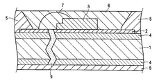
- FIG. 1 is a schematic cross-sectional view of a first embodiment of a lead frame for an optical semiconductor device according to the present invention.
- FIG. 2 is a schematic sectional view of a second embodiment of the lead frame for an optical semiconductor device according to the present invention.
- FIG. 3 is a schematic sectional view of a third embodiment of the lead frame for an optical semiconductor device according to the present invention.
- FIG. 4 is a schematic cross-sectional view of a fourth embodiment of the lead frame for optical semiconductor devices according to the present invention.
- FIG. 5 is a schematic sectional view of a fifth embodiment of a lead frame for an optical semiconductor device according to the present invention.
- FIG. 6 is a schematic sectional view of a sixth embodiment of a lead frame for an optical semiconductor device according to the present invention.
- FIG. 7 is a schematic sectional view of a seventh embodiment of the lead frame for an optical semiconductor device according to the present invention.
- FIG. 8 is a graph showing the reflectance of the lead frame for an optical semiconductor device of Invention Example 19 according to the present invention together with the reflectance of Conventional Example 1.
- a metal such as silver or a silver alloy or a layer of an alloy thereof as a reflective layer is initially formed by a plating method, and further, mechanical processing (for example, plastic processing such as rolling) is performed on the layer. Then, the metal structure (plating structure) formed by the plating method has a reflective layer in which at least the surface thereof is mechanically deformed by mechanical processing.
- the plating method may be a wet plating method such as an electroplating method or an electroless plating method, or a dry plating method such as a sputtering method.
- the mechanical processing may be plastic processing such as rolling or pressing, or mechanical polishing using colloidal silica or the like.
- plastic processing such as rolling or pressing, or mechanical polishing using colloidal silica or the like.
- the entire material including the base body undergoes plastic working, so that the entire plated structure undergoes plastic deformation.
- mechanical polishing the surface of the plated structure is smoothed and subjected to mechanical deformation including the surface of the substrate.
- the metallographic structure (plating structure) formed by electroplating, electroless plating, or sputtering is applied to the plating structure by plastic working such as rolling or pressing, or mechanical polishing. It has a reflective layer whose surface is mechanically deformed at least on the outermost surface.
- the plastically deformed metal structure is different from the cast structure as is metallurgically clear in the present technical field, and is also different from the plated structure before deformation formed by plating. Specifically, fine crystals are usually observed on the surface after plating, and a needle-like structure, a precipitated state of spherical particles, and the like are observed.
- the surface state after rolling or pressing after plating exhibits surface properties such that the processing pattern formed on the rolls of the rolling rolls or the surface of the press mold is transferred to the lead frame side. Therefore, the surface can be clearly distinguished by performing surface observation with a general-purpose SEM at an observation magnification of 2000 to 10,000 times, for example.
- a general-purpose SEM at an observation magnification of 2000 to 10,000 times, for example.
- mechanical polishing is performed after plating, it can be confirmed that the processing alteration layer seen by the polishing streaks and cross-sectional observation of the abrasive paper and abrasive grains is formed on the outermost layer. It can be clearly distinguished from later states.
- the lead frame of the present invention not only the wavelength range of 340 to 400 nm but also the visible light wavelength range of 400 to 800 nm can reach the physical theoretical value of the reflectance of silver as much as possible. This is because the reflectivity is about 98% at a wavelength of 450 nm when pure silver is formed on a mirror substrate such as silicon by sputtering. However, it is easy to use a brightener by simply plating. It is a numerical value that cannot be achieved. In the case of a film made of a metal other than silver or an alloy thereof, a high reflectance in the near ultraviolet region to the visible light region required as an optical semiconductor lead frame can be achieved.
- the present inventors cause mechanical deformation in the plated structure by performing mechanical processing such as rolling after plating, reduce fine irregularities by crushing the plated structure, and reduce crystal grain boundaries. As a result of extinction, the light absorption phenomenon was reduced to the limit. As a result, it was clarified that the reflectance can be brought close to the theoretical value even in the visible light region. As a result, by using the lead frame according to the present invention, excellent luminance can be obtained even in a conventional optical semiconductor device in the visible light region, and a blue light emitting element having a wavelength region of 400 to 800 nm, particularly an emission wavelength of around 450 nm is mounted. It is suitably used for an optical semiconductor device.
- the reflective layer made of a metal or an alloy thereof according to the present invention is formed on the outermost surface of at least a portion that contributes to light reflection (that is, at least a region that reflects light emitted from the optical semiconductor element). It only has to be. In other portions, it is not necessary to provide a reflective layer, and even if a layer other than the reflective layer is formed, there is no particular problem in terms of reflectance.
- a plating method for example, electroplating method, electroless plating method or sputtering method
- a conductive substrate for example, strip material
- a reflective layer made of a metal or an alloy thereof, such as silver or a silver alloy
- mechanical processing such as rolling, pressing, or mechanical polishing (for example, polishing using colloidal silica) is performed.
- the shape of the lead frame is formed by pressing or etching.
- a chip mounting portion is formed on the lead frame by a resin mold or the like, and an optical semiconductor module is manufactured by mounting an optical semiconductor chip, wire bonding, and sealing with resin or glass containing a phosphor.
- a conductive base such as a strip
- silver plating or gold / palladium / nickel plating is performed.
- it attaches to predetermined heat processing after metal plating, and makes the particle size of a plating layer coarse.
- the present invention and the conventional method are the ones in which the present invention is a modification of the plating structure as a mechanical processing finish, whereas the conventional method is a simple processing finish by cladding, plating finish or heat treatment finish, or The structure is completely different in that the heat treatment for plating and rolling is improved.
- the processing rate (or area reduction rate) at the time of plastic processing such as rolling or pressing after forming the reflective layer is 1% or more in the portion used as the reflective layer.
- the higher the processing rate the better the reflection characteristics and the higher the brightness of the LED lead frame. If the processing rate during plastic processing such as rolling after forming the reflective layer exceeds 80%, not only the effect of improving the reflection characteristics is saturated, but also cracks and cracks during bending are likely to occur. % Or less is preferable.
- the “machining rate” indicates a ratio represented by “(plate thickness before processing ⁇ plate thickness after processing) ⁇ 100 / (plate thickness before processing)”.
- location used as a reflective layer means that when an optical semiconductor module is formed, an optical semiconductor module is obtained by resin-molding a portion other than the light emitting portion, but the optical semiconductor chip emits light. In this case, it means a portion where the lead frame is exposed and a portion where light reflection occurs.
- the lead frame for an optical semiconductor device of the present invention has good reflectance characteristics and can easily form a film by using copper or a copper alloy, iron or an iron alloy, or aluminum or an aluminum alloy as a base.
- a lead frame that can contribute to cost reduction can be provided.
- the lead frame based on these metals or alloys has excellent heat dissipation characteristics, and the heat energy generated when the light emitter emits light can be smoothly discharged to the outside through the lead frame, and light emission It is expected that the lifetime of the element will be prolonged and the reflectance characteristics will be stabilized over a long period of time. This depends on the conductivity of the substrate, preferably at least 10% in IACS (International Annealed Copper Standard), more preferably 50% or more.
- IACS International Annealed Copper Standard
- the lead frame for an optical semiconductor device of the present invention has a reflective layer thickness of 0.2 ⁇ m or more after mechanical processing such as rolling made of metal or an alloy thereof, for example, silver or a silver alloy,
- the reflectivity can be stably increased, and deterioration due to heating in a subsequent process such as wire bonding, sealing with resin or glass can be suppressed.
- the upper limit of the thickness of the reflective layer after mechanical processing such as rolling is preferably 10 ⁇ m or less from the viewpoint of reduction of silver as a noble metal and plating processing cost. When it is thinner than the lower limit (for example, 0.1 ⁇ m), discoloration due to heating occurs and the rate of improvement in reflectance is small. For this reason, in order to prevent discoloration due to heating more stably, the thickness of the reflective layer after mechanical processing such as rolling is preferably 0.5 ⁇ m or more.
- the silver or silver alloy forming the reflective layer in the lead frame for optical semiconductor devices of the present invention is silver, silver-tin alloy, silver-indium alloy, silver-rhodium alloy, silver-ruthenium alloy, silver-gold alloy, By using a material selected from the group consisting of a silver-palladium alloy, a silver-nickel alloy, a silver-selenium alloy, a silver-antimony alloy, and a silver-platinum alloy, a lead frame with good reflectivity and good productivity can be obtained.
- silver, silver-tin alloy, silver-indium alloy, silver-palladium alloy, silver-selenium alloy, or silver-antimony alloy are more preferable from the viewpoint of improving the reflectance.
- nickel, nickel alloy, cobalt, cobalt alloy, copper, and the like are provided between the base and the reflective layer made of metal or an alloy thereof (for example, silver or silver alloy).
- An intermediate layer made of a metal or alloy selected from the group consisting of copper alloys may be provided.
- the intermediate layer is suitably formed by plating, for example.
- the thermal conductivity of the material is relatively low. Therefore, by providing a copper or copper alloy layer as an intermediate layer, the heat dissipation can be improved without impairing the reflectance. Furthermore, since the plating layer which is the copper or copper alloy layer contributes to the improvement of plating adhesion, it is possible to prevent deterioration of adhesion due to heat generation when the light emitting element emits light.
- a nickel, nickel alloy, cobalt, or cobalt alloy layer is used as an intermediate layer in order to suppress diffusion of the substrate component to the reflective layer due to heat generated when the light emitting element emits light. It is effective to provide it.
- the improvement of the resin is also progressing, and in some cases, glass sealing is being performed, and during the sealing process with resin or glass
- the processing temperature is also rising.
- an optical semiconductor device such as an LED
- the diffusion phenomenon is expected to proceed due to heat generated by the LED chip.
- it is effective to provide an intermediate layer.
- the thickness of these intermediate layers is not particularly limited in the present invention, but is preferably in the range of 0.08 to 2.0 ⁇ m.
- the thickness of the intermediate layer is particularly preferably in the range of 0.2 to 2.0 ⁇ m.
- the processing rate at the time of mechanical processing such as rolling after forming the reflective layer is set to 1% or more as the processing rate based on the plate thickness immediately after the initial formation of the reflective layer (immediately after plating).
- a lead frame having a reflectance improved by several percent over silver or a silver alloy film obtained by the plating method can be obtained even at a wavelength of 400 to 800 nm, which is a visible light region, while preventing a decrease in reflectance due to the appearance of an absorption peak.
- the processing rate at the time of mechanical processing, such as rolling processing after formation of a reflective layer is less than 1%, mechanical deformation such as plastic deformation is insufficient, and its effect is small.
- the number of rolling is preferably 3 times or less at most.
- the processing rate at the time of rolling after the reflective layer is formed may be 1% or more in each rolling.
- the processing rate during the rolling process after the formation of the reflective layer is 10% or more in total.
- the processing rate at the time of rolling after forming the reflective layer is too large, the plating thickness increases at the time of initial formation of the reflective layer (during plating), resulting in not only an increase in plating cost but also an environmental load.
- the processing cost increases due to the increase in the number of rolling processes after the reflective layer is formed and the effect of improving the reflectance is saturated, the reflective layer is formed because the cracks and cracks are likely to occur during bending.
- the processing rate in the subsequent rolling process is 80% or less in total.
- the total processing rate is more preferably 20 to 60% in consideration of bending workability.
- heat treatment also referred to as tempering or low-temperature annealing
- a technique such as batch type or running type after mechanical processing such as rolling.
- the bonding force between the crystal grains can be strengthened at the crystal grain boundaries to narrow the intergranular spacing, but it is necessary to limit the heat treatment to a level that does not lower the reflectivity.
- the conditions for the heat treatment performed after mechanical processing such as rolling are not particularly limited.
- the heat treatment is performed at a temperature of 50 to 150 ° C. for 0.08 to 3 hours. It is preferable. If the temperature of this heat treatment is too high or the time is too long, the heat history becomes excessive and the reflectance is lowered.
- the reflective layer on the surface made of a metal such as silver or a silver alloy or an alloy thereof may be formed by wet plating using an electroplating method or an electroless plating method, or alternatively, the metal may be formed by sputtering.
- the substrate surface may be formed by plating and precipitating.
- the electroplating method has been described as a representative example.
- a metal such as silver or a silver alloy is used in the same manner as in the case of the electroplating method.
- a layer made of the alloy can be formed.
- the electroless plating method it may be formed by using a commercially available bath (for example, S.Dia. Ag40; manufactured by Sasaki Chemical Co., Ltd.), etc. Can be used.
- the thickness of the reflective layer made of a metal such as silver or silver alloy or an alloy thereof after mechanical processing such as rolling is not particularly limited, but may be in the range of 0.5 to 10 ⁇ m. preferable.
- the coating thickness (initial thickness) before processing for achieving the thickness after mechanical processing is not particularly limited, but is preferably in the range of 1 to 50 ⁇ m, for example.
- Mechanical processing to a material in which a part or all of the conductive substrate is coated with a metal such as silver or a silver alloy or an alloy thereof can be performed, for example, by rolling with a cold rolling mill.
- the rolling machine includes a 2-stage roll, a 4-stage roll, a 6-stage roll, a 12-stage roll, a 20-stage roll, and the like, and any rolling machine can be used.
- the processing rate (area reduction rate) in rolling or pressing is 1% or more, preferably 10% or more, and the gap between the grain boundaries of silver or silver alloy is sufficiently narrowed to form a plastic deformation structure. Can do.
- the rolling roll used for the rolling process is preferably less than 0.1 ⁇ m in terms of the arithmetic average (Ra) of the surface roughness in consideration of improving the reflectance on the lead frame side formed by transferring the rolls.
- Ra arithmetic average
- plastic processing by cold rolling processing has been described, but in the case of press processing (for example, coining) or mechanical polishing (for example, polishing by colloidal silica), it is always the case.
- press processing for example, coining
- mechanical polishing for example, polishing by colloidal silica
- plastic processing and mechanical surface processing can be performed in the same manner as in the case of cold rolling.
- it can be achieved by adjusting the working rate by pressure adjustment at a press pressure of 0.1 N / mm 2 or more and plastically deforming.
- colloidal silica having a particle size of 10 to 300 nm is dispersed to control the number of polishing seconds and adjust the degree of processing.
- the degree of processing varies depending on the abrasive grains used and the polishing time. For example, in the case of polishing with colloidal silica (OP-S suspension: manufactured by Marumoto Struers), 10 to 60 seconds. It is preferable to set the polishing time as follows.
- the optical semiconductor device of the present invention is provided at least at a place where light generated from the optical semiconductor element is reflected by plating made of a metal such as silver or a silver alloy or an alloy thereof, and is mechanical such as a rolling process.
- a metal such as silver or a silver alloy or an alloy thereof
- the lead frame of the present invention having a reflective layer with a layer whose whole is plastically deformed or at least its surface is mechanically deformed by processing, it is possible to effectively obtain reflectance characteristics at low cost. be able to. This is because the reflectance characteristics are sufficiently effective by forming a reflective layer made of silver or a silver alloy only on the mounting portion of the optical semiconductor element.
- the optical semiconductor element mounting surface of the double-sided plating material may be thickened and the non-mounting surface may be thinned.
- a reflective layer made of a metal such as silver or a silver alloy or an alloy thereof may be partially formed, and formed by partial plating such as single-sided plating, stripe plating, spot plating, etc. It may be formed by mechanical processing. Manufacturing a lead frame in which the reflective layer is partially formed can reduce the amount of metal used in the part where the reflective layer is unnecessary, so that a lead frame with a low environmental load can be obtained. Fewer optical semiconductor devices can be obtained.
- the substrate is exposed to the end face of the lead frame inevitably obtained because it is processed into a predetermined lead frame shape by performing stamping or etching. If the lead frame after pressing or etching is stored with the substrate exposed, there is a concern about corrosion of the substrate component or deterioration of solderability to the surface of the substrate.
- the exposed area of the substrate is very small with respect to the entire surface, and there is almost no effect on the solderability with external leads. Further, the exposure of the substrate does not cause a problem even in the case of a thin plate thickness or a wide lead width. However, in the case of a thick plate thickness or a narrow lead width, soldering with a lead may affect the soldering, and the reliability of soldering is enhanced when the external lead is plated.
- solder wetting is improved by applying a plating film (soldering improvement layer) with good solder wetting, such as silver, tin, gold, and alloys of these, at least on the external lead parts that are soldered outside the reflective area .
- soldering improvement layer good solder wetting, such as silver, tin, gold, and alloys of these, at least on the external lead parts that are soldered outside the reflective area .
- the plating type may be a metal type that achieves the purpose, such as silver, tin, gold, or alloy plating thereof.
- the reflective layer is further subjected to plastic processing such as rolling or pressing, or mechanical polishing.
- plastic processing such as rolling or pressing, or mechanical polishing.
- the plated structure made of silver is characterized in that at least the surface is mechanically deformed. By causing mechanical deformation in the plating layer, the bonding force of the grain boundaries of the crystal formed by plating is strengthened and dislocations are discharged. At the same time, silver is recrystallized by the energy of plastic processing, and at the same time The unevenness can be smoothed by a mechanically acting force.
- the reflectance at a wavelength of 400 to 800 nm can be improved, so that it is suitably used particularly for an optical semiconductor device on which an optical semiconductor light emitting chip with a wavelength of 450 nm to 800 nm is mounted.
- optical semiconductor devices it is particularly effective for LEDs.
- it has an excellent effect in improving the reflectance in the near ultraviolet region.
- the plating structure remaining ratio that has not been mechanically processed is preferably 50% or less, and more preferably 30% or less of the region in the location used as the reflective layer.
- the plating structure residual rate typically means that when a silver plating layer is formed by an electroplating method, a plating structure (a needle-like structure or a precipitated state of spherical particles) is formed over almost the entire area. Even if mechanical processing is applied to cause mechanical deformation and the plating structure disappears, if the shape that resembles the plating structure remains on the subsequent surface, the area of the shape similar to the remaining plating structure Ratio [area of shape similar to remaining plating structure / area of measurement target area] (%).
- the plating structure or a shape similar thereto may not remain at all, so the lower limit of the plating structure remaining rate is 0%.
- the plating structure remaining rate is preferably closer to 0%, and from the viewpoint of improving the reflectance, the plating structure remaining rate is most preferably 0%.
- the “location used as the reflective layer” means that the LED module is formed by resin molding other than the light emitting portion when forming the LED module, but the lead frame when the LED chip emits light. It shows the part where the light reflection phenomenon occurs at the exposed part.
- the plating structure remaining rate at the exposed portion of the lead frame that contributes to the reflection phenomenon is 50% or less, and the plating structure remaining rate of 50% or less on the entire surface is naturally good. Processing may be performed so that the plating structure remaining rate of the portion is 50% or less, and only that region becomes a portion used as a reflective layer of the LED.
- long-term reliability can be ensured by setting the thickness of the reflective layer made of silver after mechanical deformation to 0.2 ⁇ m or more.
- the thickness is 10 ⁇ m or less, the cost can be reduced without using a precious metal more than necessary. This is because the effect of long-term reliability is that the thickness of the reflective layer is saturated at 10 ⁇ m. The effect is sufficiently expected when the thickness is 0.2 to 10 ⁇ m, but preferably 0.5 to 7 ⁇ m, and more preferably 1 to 5 ⁇ m.
- the reflective layer coating thickness after mechanical deformation made of silver is less than 0.2 ⁇ m, the copper component of the substrate is likely to diffuse to the surface, so that the outermost layer coating thickness is at least 0.2 ⁇ m or more. It means that it is preferably formed. Actually, a material having the above lower limit value or more was produced, and it was confirmed that the heat resistance was increased as compared with a material having a value below this value. Note that if the reflective layer is made of a silver alloy, it may be difficult to ensure 90% of the reflectance at a wavelength of 400 to 800 nm. Therefore, silver is preferably used for the reflective layer in this embodiment, and the purity is 99% or more. Preferably there is.
- the rolling processing rate is relative to the plate thickness after plating. Is preferably 10% or more, and more preferably 40% or more. It is preferable to manufacture the lead frame for optical semiconductors in such a processing rate range so that the plating structure residual rate can be easily adjusted to a suitable range.
- the rolling process rate is equal to or more than the above lower limit value, the plating structure remaining rate is less affected by the roughness of the rolling roll, so that the plating structure remaining rate is stably 50% or less without depending on the roll roughness. And the reflectance can be sufficiently increased.
- the rolling rate there is no particular upper limit for the rolling rate, but it must be determined after adjusting the strength, hardness, and conductivity required for the material. If the rolling rate is high, the power required for the rolling mill is high. Not only does it increase and the environmental impact increases, but cracks and cracks during bending work tend to occur, so the upper limit is practically about 80%. It should be noted that the rolling process may be repeated any number of times from the plate thickness after plating to the product plate thickness of the optical semiconductor lead frame. By setting the number of rolling times to several times, the probability that the rolling roll comes into contact with the plated structure is increased, and as a result, it is easy to reduce the remaining ratio of the plated structure. Even 5 times or less is preferable. Note that the rolling roll used for the rolling process has an arithmetic average (Ra) of surface roughness of less than 0.1 ⁇ m in consideration of improving the reflectance on the lead frame side formed by transferring the rolls. preferable.
- Ra arithmetic average
- the press processing rate is preferably 10% or more with respect to the plate thickness after plating as in the rolling processing. 40% or more is more preferable. It is preferable to manufacture the lead frame for optical semiconductors in such a processing rate range so that the plating structure residual rate can be easily adjusted to a suitable range.
- the conditions of press work are not limited, for example, it can be plastically deformed by setting the press pressure to 0.1 N / mm 2 or more.
- the upper limit of the pressing rate is not particularly set, but in reality, the upper limit is about 80%.
- heat treatment may be performed by a technique such as a batch mold or a running mold after rolling or pressing, and a tempering step may be performed, but the degree of reflectance is not reduced. It is necessary to keep it in the heat treatment. Preferred conditions for this heat treatment are as described above.
- the macro surface roughness in the present invention is a surface roughness obtained by a measurement distance of a contact type surface roughness meter. Specifically, small undulations of the substrate itself appear as numerical values.
- the measurement distance is appropriate between several mm to several tens mm, and the experimental result shows that the measurement distance of 4 mm best represents the macroscopic surface roughness and has a correlation with the resin adhesion.
- the surface roughness Ra was determined by a method based on JIS B 6010-2001, and measured in 5 points in each of the two directions, ie, the rolling direction and the vertical direction, and the average value was defined as the macroscopic surface roughness.
- the micro surface roughness in the present invention is a surface roughness obtained in an observation field of an atomic force microscope (AFM).
- This micro surface roughness cannot be measured with a macro surface roughness, but greatly affects the reflectance. Specifically, the frequency of dendritic precipitation after plating appears as this value. It was found that unevenness on the surface of the order of several tens of nanometers is a cause of reducing the reflectance. In order to measure this micro surface roughness, it is appropriate to use an AFM and measure within a field of several to several tens of microns. From the results of experiments, a field of view of 6.16 microns ⁇ 6.16 microns. It was found that the measurement by means best represents the micro surface roughness and has a correlation with the reflectance.
- the surface roughness Sa was determined with a field of view of 6.16 microns ⁇ 6.16 microns.
- measurements were taken at any five points on the lead frame, and the average value was set to a micro surface roughness.
- the macro surface roughness While maintaining the macro surface roughness as much as possible, by suppressing the micro surface roughness as much as possible, it has excellent reflectivity for both light in the near ultraviolet region of wavelength 340 to 400 nm and visible light region of 400 nm to 800 nm, It has been found that a lead frame for a semiconductor device having high resin adhesion can be obtained. Based on this finding, the present invention has been made.
- the surface roughness is measured as a micro surface roughness by AFM, and the height of surface undulation is measured as a macro surface roughness by a stylus type surface roughness meter.
- Macro surface roughness can be determined by intermediate rolling or final rolling of the substrate. It is possible to change the macro surface roughness by changing the rolling conditions and roll number.
- the micro surface roughness can be changed by subjecting the outermost surface after plating to a treatment such as mechanical polishing using fine particles. For example, in the case of mechanical polishing, it is possible to change the micro surface roughness by changing the count and polishing time. Further, as non-contact polishing, methods such as chemical polishing and electrolytic polishing may be used.
- metal plating is performed on both surfaces or one surface of a conductive material.
- Metal plating is performed by a method of depositing on the surface of the metal material by electroplating.
- the metal plating film is formed of any one of Au, Ag, Cu, Pt, Al, Rh, or an alloy thereof. Ag or an alloy thereof is preferable.
- the metal plating method itself can be performed by a normal method.
- the resulting plated surface is smoothed by polishing with colloidal silica or the like.
- any means for smoothing the plating surface may be used, and for example, plastic processing such as the above-described rolling processing or press processing may be used.
- the thickness of the metal plating film itself on the metal substrate can be determined by the plating conditions and the method of subsequent processing, and is preferably 0.01 to 20 ⁇ m, more preferably after the above polishing or plastic processing. Is 0.1 to 10 ⁇ m.
- substrate Copper or a copper base alloy or iron or an iron base alloy etc. are used.
- the base is preferably a copper alloy strip having a conductivity of 60% IACS or more from the viewpoint of heat dissipation of the lead frame for optical semiconductor devices.
- a copper alloy material having a conductivity of 60% IACS or higher CD19 listed alloys C19400, C14410, Furukawa Electric Co., Ltd. EFTEC64T (C18045) (trade name), and the like can be used.
- the macro surface roughness is changed to some extent by changing the roll roughness at the time of finish rolling to be applied last. Since actual strip products vary to some extent, a strip having a desired roughness is selected from strips created by varying the conditions, and the plating is applied thereto.
- a substrate having a small macro surface roughness is obtained, and when the roll roughness is large, a substrate having a large macro surface roughness is obtained.
- Macro surface roughness is measured with a stylus type surface roughness meter.
- the macro surface roughness is preferably such that Ra is 0.010 ⁇ m or more, more preferably 0.020 ⁇ m or more, further preferably 0.030 ⁇ m or more, and most preferably 0.040 ⁇ m or more.
- resin adhesiveness improves.
- the macro surface roughness exceeds 0.100 ⁇ m, the undulation (heaviness of the undulation) of the substrate surface increases, and the sealing material does not sufficiently enter the undulation valley.
- the macro surface roughness is preferably 0.060 ⁇ m or less.
- “improvement of resin adhesion” means that peeling does not occur in the resin adhesion test evaluated in Examples described later.
- the surface of the plating film is processed.
- the micro surface roughness is regulated.
- the micro surface roughness is obtained by measurement at a viewing angle of 6.16 ⁇ m ⁇ 6.16 ⁇ m using an atomic force microscope.
- the micro surface roughness Ra is preferably 50 nm or less, more preferably 30 nm or less, particularly preferably 10 nm or less, and most preferably 5 nm or less, whereby the reflectance of the LED component material is improved.
- “improvement of reflectance” means having a preferable reflectance described below.
- the micro surface roughness is about 2.0 nm or less, the resin adhesion is reduced regardless of the macro surface roughness, and therefore the micro surface roughness is preferably 3.0 nm or more. Since a plating layer made of a metal such as Ag or an alloy thereof is formed and then passed through a rolling process, the macro surface roughness and the micro surface roughness change simultaneously. Here, it is possible to simultaneously change the macro surface roughness and the micro surface roughness by changing the rolling rate. By changing the roll roughness used for rolling, it is possible to control the micro surface roughness to some extent. Even at the same rolling ratio, if the roll roughness is small, the micro surface roughness becomes small.
- the control of the micro surface roughness directly contributes to the reflectance, and the smaller the roughness, the better the reflectance (particularly the reflectance in the ultraviolet region).
- the macro surface roughness contributes to improvement of solder wettability and resin adhesion, imparts suitable characteristics to the lead frame for optical semiconductor devices, and maintains excellent smoothness.
- the reflectance can be further improved by combining both the above-described micro surface roughness and macro surface roughness within the preferable range. This has nothing to do with the conventional metal recrystallized grain size and orientation as noted above.
- the preferable reflectance in the present invention is preferably the following mode. Preferred conditions will be described in the order of the following (a), (b), (c), and (d). The following (d) is the most preferable condition.
- a metal plating film is gold
- the total reflectance is 30% or more in the entire region of the near ultraviolet light region (for example, 375 nm) and the visible light region (for example, 400 to 800 nm), and the total reflectance on the long wavelength side in the visible light region is particularly high.
- the metal plating film is copper, the following modes are preferred.
- the total reflectivity is 35% or more in the entire region of the near ultraviolet light region (for example, 375 nm) and the visible light region (for example, 400 to 800 nm), and the total reflectance on the long wavelength side in the visible light region is particularly high.
- the metal plating film is platinum, the following embodiments are preferable.
- the total reflectance is 55% or more in the visible light region (for example, 400 to 800 nm), and the total reflectance is 55% or more in the near ultraviolet light region (for example, 375 nm). Furthermore, when a metal plating film is aluminum, the following aspects are preferable.
- the total reflectance is 85% or more in the visible light region (for example, 400 to 800 nm), and the total reflectance is 95% or more in the near ultraviolet region (for example, 375 nm).
- the metal plating film is rhodium, the following embodiments are preferable.
- the total reflectivity is 75% or more in the entire region of the near ultraviolet light region (for example, 375 nm) and the visible light region (for example, 400 to 800 nm), and the total reflectance on the long wavelength side in the visible light region is particularly high.
- Silver or silver alloy plating and metal plating other than these can be performed by a method of depositing on the surface of the metal material by electroplating, electroless plating or sputtering.
- the silver or silver alloy plating film is not particularly limited, and pure silver, silver-antimony alloy, silver-selenium alloy, silver-indium alloy, silver-tin alloy, silver-gold alloy and the like can be used.
- the thickness of the plating is not particularly limited, but is usually in the range of 0.2 to 10 ⁇ m after the plastic working. A material in which a part or all of the conductive substrate is coated with silver, a silver alloy, or a metal other than these is rolled by a cold rolling mill.
- the lead frame of this embodiment after the reflective layer 2 is formed by electroplating or the like, plastic deformation or the like is generated by, for example, rolling, and the near ultraviolet and visible light regions (wavelengths of 340 nm to 800 nm) are generated.
- the lead frame for an optical semiconductor device is excellent in reflection characteristics.
- 3 and 4 are schematic cross-sectional views of the third and fourth embodiments in which a reflective layer deformed by rolling after electroplating, for example, is disposed only on one side on which the optical semiconductor element is mounted. 3 differs from FIG. 4 in the presence or absence of the intermediate layer 4.
- the soldering improvement layer 7 is formed on the surface where the reflective layer is formed and on a portion other than the portion where the reflectance is required (that is, at least the region where the light emitted from the optical semiconductor element is reflected). There is no problem even if it is provided.
- the unit of the number before each element is mass%.
- “A1100”, “A2014”, “A3003”, and “A5052” represent aluminum or aluminum alloy substrates, each of which is specified in Japanese Industrial Standards (JIS H 4000: 2006, etc.).
- “42 Alloy” represents an iron-based substrate, containing 42% by mass of nickel, and the balance of iron and inevitable impurities.
- the substrate was aluminum, it was subjected to a process of electrolytic degreasing, pickling and zinc replacement treatment, and in the case of other substrates, a pretreatment was performed through the steps of electrolytic degreasing and pickling.
- silver strike plating was performed, and the outermost layer plating thickness was expressed as the thickness after rolling including the silver strike plating thickness.
- Example 1 The pretreatment conditions in Example 1 are shown below.
- (Pretreatment conditions) [Cathode electrolytic degreasing]
- Degreasing solution NaOH 60 g / liter
- Degreasing conditions 2.5 A / dm 2 , temperature 60 ° C., degreasing time 60 seconds
- Pickling solution 10% sulfuric acid pickling condition: 30 seconds immersion, room temperature [zinc substitution] (used when the substrate is aluminum)
- Zinc replacement solution NaOH 500 g / liter, ZnO 100 g / liter, tartaric acid (C 4 H 6 O 6 ) 10 g / liter, FeCl 2 2 g / liter
- Treatment conditions 30 seconds immersion, room temperature [Ag strike plating] coating thickness 0.01 ⁇ m
- Plating solution KAg (CN) 2 5 g / liter, KCN 60 g / liter
- Plating conditions current density 2 A / dm 2 , plating time 4 seconds, temperature 25
- Example 1 The liquid composition and plating conditions for the reflective layer plating used in Example 1 are shown below.
- the reflectance at a wavelength of 340 nm is 60% or more, the reflectance at 375 nm is 75% or more, the reflectance at 400 nm is 80% or more, and 90% or more at wavelengths of 450 nm and 600 nm in the visible light region.
- Patent Document 2 is an alumina substrate made of ceramics, whereas a lead frame material using a metal for the substrate as in the present invention is subjected to a heat treatment at 320 ° C. for 30 seconds. It is thought that diffusion of the base material and the substrate component occurs, and further, the heat treatment is performed in the atmosphere, so that the oxidation of the substrate component proceeds and the heat resistance is lowered as shown in Table 2. It is. Moreover, when Ag thickness is thin, it turns out that it exists in the tendency which is inferior to heat resistance, as it exists in the prior art examples 2 and 4.
- the outermost layer since the outermost layer has a coating thickness of 0.1 ⁇ m, it is inferior in heat resistance and improved in reflectance at wavelengths of 375 nm and 400 nm, but inferior to Invention Example 11, It can be seen that the surface coating thickness is preferably 0.2 ⁇ m or more. Further, in Reference Example 2, since the processing rate at the time of rolling after forming the reflective layer is as low as 0.5%, the reflectance is improved as compared with that without rolling, but the level is not sufficient. Further, in Reference Example 3, although the area reduction rate is over 80%, it was confirmed that the reflectivity and heat resistance were excellent, but the bending workability was inferior. Therefore, it can be seen that the area reduction rate is preferably 1 to 80%.
- Reference Example 4 and Reference Example 5 are examples in which heat treatment (low temperature annealing) was performed after plating and rolling, but the reflectivity was reduced by about 10% overall, and the thermal history due to low temperature annealing was excessive. As a result, the reflectance decreased. Thus, it can be seen that when heat treatment is performed after rolling, it is necessary to apply it while fully considering the reflectance.
- FIG. 8 shows the measurement results of the reflectance in Conventional Example 1 and Inventive Example 19. These are the results obtained by comparing the conventional example 1 which has been plated by a conventional ordinary method (no plastic working or heat treatment) and the inventive example 19 which has been subjected to plastic working after plating.
- the example of the present invention has extinction of the absorption peak at a wavelength of 345 to 355 nm and exhibits a very excellent reflectance in the visible light region.
- This reflectivity is very close to the physical limit reflectivity of silver and shows an unprecedented reflectivity, and is very suitable for use as a lead frame for optical semiconductor devices in the wavelength range of 340 to 800 nm from the near ultraviolet to the visible light region. I understand that I can do it.
- the result of the conventional example 1 shown in the figure seems to have a lower reflectance on the lower wavelength side than the case of the conventional example 3.
- Example 2 As Example 2, a substrate having a width of 100 mm shown in Table 3 was pretreated in the same manner as in Example 1, and then electroplating treatment shown in Table 3 was performed in the same manner as in Example 1. Using a substrate having a plate thickness of 0.25 mm and 0.83 mm, Ag plating is performed on both sides of the substrate so that the Ag coating thickness after the rolling process is 3 ⁇ m, and then processing during the rolling process after forming the reflective layer Rolling was performed at a rate of 40% to obtain strips having sheet thicknesses of 0.15 mm and 0.5 mm.
- the total reflectance is 60% or more at a wavelength of 340 nm, 75% or more at a wavelength of 375 nm, 80% or more at a wavelength of 400 nm, and a visible light region.
- the required characteristics were 90% or more at wavelengths of 450 nm and 600 nm.
- Solder type Sn-3Ag-0.5Cu Temperature: 250 ° C
- Flux Isopropyl alcohol-25% rosin Immersion speed: 25 mm / sec Immersion time: 10 seconds
- Immersion depth 10 mm
- Example 2 the following was found in the present invention example, the reference example, and the conventional example.
- A If the plated Ag coating has a rolled reflective layer of 3 ⁇ m, the reflectance is as good as in Example 1.
- B It was found that none of the inventive examples in which Ag, Sn, or Au was plated on the external lead as a plating film having good solder wettability had a problem of solderability.
- C In the reference example in which the external lead is not plated with good solder wetting, there is no problem with a thin plate thickness and a wide width, but with a narrow width, the wetting time is slightly long. A thick plate and a wide width have a slightly longer wetting time, and a narrow width has a considerably longer wetting time.
- the conventional example 101 is a normal silver-plated product, but the reflectance at a wavelength of 400 nm is 85% or less, and further, the reflectance is 85% at a wavelength of 450 nm.
- the brightness is as high as 5 to 10%.
- This is expected to be suitably used for optical semiconductors utilizing these wavelengths due to improved reflectivity.
- Conventional Example 102 is an example in which heat treatment was performed after silver plating to increase the crystal grain size to 0.5 ⁇ m or more, but the initial reflectivity was slightly lower than 85% at a wavelength of 400 nm, It turns out that the nature is inferior.
- the macro surface roughness was controlled by changing the roll roughness during finish rolling.
- a substrate having a small surface roughness was obtained when the roll roughness was small, and a substrate having a large surface roughness was obtained when the roll roughness was large.
- the skin pass roll (the surface is smoother than the following 0.1S roll), 0.1S roll, 0.2S roll, 0.4S roll, 0.8S in order of increasing surface roughness Rz of the roll. I used a roll.
- the roll surface is smooth in the order of skin pass roll, 0.1S roll, 0.2S roll, 0.4S roll, and 0.8S roll.
- the macroscopic surface roughness is controlled so that the erosive macroscopic surface roughness obtained in this way becomes Ra ⁇ 0.005 ⁇ m, 0.01 ⁇ m, 0.02 ⁇ m, 0.03 ⁇ m, and 0.04 ⁇ m, respectively. did.
- a sample having a different surface shape on the metal substrate is used, and colloidal silica (OP-S suspension (OPSIF-5 liters included): Polishing by Marumoto Struers Co., Ltd.) was performed for the time shown in Table 6 so that the desired micro surface roughness was controlled.
- 0 second means a plated sample that has not been polished.
- the total reflectance is 80% or more in the visible light region (400 to 800 nm) and the total reflectance is 70% or more in the near ultraviolet light region (for example, 375 nm), each is acceptable, and a reflectance less than this is regarded as unacceptable. To do. Table 6 shows the total reflectance for each wavelength. From the results of continuous measurement, it has been confirmed that the total reflectance does not drop sharply between wavelengths.
- Plating solution CuSO 4 .5H 2 O 250 g / liter, H 2 SO 4 50 g / liter, NaCl 0.1 g / liter Plating condition: current density 6 A / dm 2 , temperature 40 ° C.
- Pt plating Plating solution: Pt (NO 2 ) (NH 3 ) 2 10 g / liter, NaNO 2 10 g / liter, NH 4 NO 3 100 g / liter, NH 3 50 ml / liter Plating conditions: current density 5 A / dm 2 , temperature 80 ° C.
- the rolling rate (%) is a value expressed as a percentage (%) obtained by dividing the difference between the cross-sectional area of the material before rolling and the cross-sectional area after rolling by the cross-sectional area of the material before rolling. .
- the results are shown in Table 8 below.
Landscapes
- Chemical & Material Sciences (AREA)
- Engineering & Computer Science (AREA)
- Chemical Kinetics & Catalysis (AREA)
- Electrochemistry (AREA)
- Materials Engineering (AREA)
- Metallurgy (AREA)
- Organic Chemistry (AREA)
- Microelectronics & Electronic Packaging (AREA)
- Computer Hardware Design (AREA)
- Power Engineering (AREA)
- Manufacturing & Machinery (AREA)
- Crystallography & Structural Chemistry (AREA)
- Physics & Mathematics (AREA)
- Condensed Matter Physics & Semiconductors (AREA)
- General Physics & Mathematics (AREA)
- Led Device Packages (AREA)
Abstract
Priority Applications (4)
| Application Number | Priority Date | Filing Date | Title |
|---|---|---|---|
| EP11795716.7A EP2584621A4 (fr) | 2010-06-15 | 2011-06-13 | Grille de connexion pour dispositif à semi-conducteurs optique, procédé pour fabriquer une grille de connexion pour dispositif à semi-conducteurs optique, et dispositif à semi-conducteurs optique. |
| CN201180019412.4A CN102844897B (zh) | 2010-06-15 | 2011-06-13 | 光半导体装置用引线框架、光半导体装置用引线框架的制造方法以及光半导体装置 |
| KR1020127021093A KR101718575B1 (ko) | 2010-06-15 | 2011-06-13 | 광반도체 장치용 리드 프레임, 광반도체 장치용 리드 프레임의 제조방법, 및 광반도체 장치 |
| US13/714,000 US20130099270A1 (en) | 2010-06-15 | 2012-12-13 | Lead frame for optical semiconductor device, method of producing the same, and optical semiconductor device |
Applications Claiming Priority (6)
| Application Number | Priority Date | Filing Date | Title |
|---|---|---|---|
| JP2010-136596 | 2010-06-15 | ||
| JP2010136596 | 2010-06-15 | ||
| JP2010142664 | 2010-06-23 | ||
| JP2010-142664 | 2010-06-23 | ||
| JP2010157132 | 2010-07-09 | ||
| JP2010-157132 | 2010-07-09 |
Related Child Applications (1)
| Application Number | Title | Priority Date | Filing Date |
|---|---|---|---|
| US13/714,000 Continuation US20130099270A1 (en) | 2010-06-15 | 2012-12-13 | Lead frame for optical semiconductor device, method of producing the same, and optical semiconductor device |
Publications (1)
| Publication Number | Publication Date |
|---|---|
| WO2011158811A1 true WO2011158811A1 (fr) | 2011-12-22 |
Family
ID=45348210
Family Applications (1)
| Application Number | Title | Priority Date | Filing Date |
|---|---|---|---|
| PCT/JP2011/063542 WO2011158811A1 (fr) | 2010-06-15 | 2011-06-13 | Grille de connexion pour dispositif à semi-conducteurs optique, procédé pour fabriquer une grille de connexion pour dispositif à semi-conducteurs optique, et dispositif à semi-conducteurs optique. |
Country Status (6)
| Country | Link |
|---|---|
| US (1) | US20130099270A1 (fr) |
| EP (1) | EP2584621A4 (fr) |
| KR (1) | KR101718575B1 (fr) |
| CN (1) | CN102844897B (fr) |
| TW (1) | TWI536616B (fr) |
| WO (1) | WO2011158811A1 (fr) |
Cited By (5)
| Publication number | Priority date | Publication date | Assignee | Title |
|---|---|---|---|---|
| WO2015029211A1 (fr) * | 2013-08-30 | 2015-03-05 | 古河電気工業株式会社 | Corps de base pour grille de connexion de dispositif à semi-conducteurs optique, procédé de fabrication de corps de base pour grille de connexion de dispositif à semi-conducteurs optique, grille de connexion de dispositif à semi-conducteurs optique faisant appel à un corps de base pour grille de connexion de dispositif à semi-conducteurs optique, procédé de fabrication de grille de connexion de dispositif à semi-conducteurs optique et dispositif à semi-conducteurs optique |
| JP2015079841A (ja) * | 2013-10-16 | 2015-04-23 | 古河電気工業株式会社 | 光半導体装置用リードフレーム基体、光半導体装置用リードフレーム、および光半導体装置用リードフレームの製造方法 |
| CN105742459A (zh) * | 2012-05-18 | 2016-07-06 | 九尊城网络科技(深圳)有限公司 | 发光二极管及其封装方法 |
| JP2017005265A (ja) * | 2016-09-01 | 2017-01-05 | 大日本印刷株式会社 | 半導体装置 |
| JP2017011101A (ja) * | 2015-06-22 | 2017-01-12 | Shマテリアル株式会社 | Ledパッケージ及び多列型led用リードフレーム、並びにそれらの製造方法 |
Families Citing this family (8)
| Publication number | Priority date | Publication date | Assignee | Title |
|---|---|---|---|---|
| CN103354270B (zh) * | 2013-07-01 | 2016-08-24 | 宁波康强电子股份有限公司 | 一种emc封装led引线框架去溢料工艺 |
| JP6085536B2 (ja) * | 2013-08-05 | 2017-02-22 | 株式会社Shカッパープロダクツ | 銅条、めっき付銅条、リードフレーム及びledモジュール |
| DE102013224581A1 (de) | 2013-11-29 | 2015-06-03 | Osram Opto Semiconductors Gmbh | Optoelektronisches Bauelement und Verfahren zu seiner Herstellung |
| US20150364626A1 (en) * | 2014-06-11 | 2015-12-17 | Electronics And Telecommunications Research Institute | Transparent electrode and solar cell including the same |
| US9859481B2 (en) | 2014-12-22 | 2018-01-02 | Nichia Corporation | Light emitting device |
| US9590158B2 (en) | 2014-12-22 | 2017-03-07 | Nichia Corporation | Light emitting device |
| WO2018198982A1 (fr) * | 2017-04-27 | 2018-11-01 | 京セラ株式会社 | Carte de circuit imprimé et dispositif émetteur de lumière la comportant |
| JP6815507B2 (ja) * | 2017-06-29 | 2021-01-20 | 京セラ株式会社 | 回路基板およびこれを備える発光装置 |
Citations (12)
| Publication number | Priority date | Publication date | Assignee | Title |
|---|---|---|---|---|
| JPS61148883A (ja) | 1984-12-22 | 1986-07-07 | Toshiba Corp | 光半導体装置用リ−ドフレ−ム |
| JPS61156779A (ja) * | 1984-12-28 | 1986-07-16 | Toshiba Corp | 発光表示装置用電極部材の製造方法 |
| JP2003282948A (ja) * | 2002-03-20 | 2003-10-03 | Sharp Corp | 発光装置およびその製造方法 |
| JP3515226B2 (ja) | 1995-06-22 | 2004-04-05 | 古河電気工業株式会社 | 銀被覆バネ用りん青銅とその製造方法 |
| JP2005029849A (ja) | 2003-07-07 | 2005-02-03 | Kobe Steel Ltd | リフレクター用Ag合金反射膜、及び、このAg合金反射膜を用いたリフレクター、並びに、このAg合金反射膜の形成用のAg合金スパッタリングターゲット |
| JP2007194385A (ja) * | 2006-01-19 | 2007-08-02 | Stanley Electric Co Ltd | 半導体発光装置及び半導体発光装置の製造方法 |
| JP2008016674A (ja) | 2006-07-06 | 2008-01-24 | Matsushita Electric Works Ltd | 銀膜、銀膜の製造方法、led実装用基板、及びled実装用基板の製造方法 |
| JP2008277349A (ja) * | 2007-04-25 | 2008-11-13 | Kyocera Corp | 発光素子搭載用基体、及びその製造方法、ならびに発光装置 |
| JP2009135355A (ja) * | 2007-12-03 | 2009-06-18 | Hitachi Cable Precision Co Ltd | リードフレーム及びその製造方法並びに受発光装置 |
| JP2010136596A (ja) | 2008-12-08 | 2010-06-17 | Nippon Densan Corp | モータ |
| JP2010142664A (ja) | 2010-02-18 | 2010-07-01 | Sammy Corp | 弾球遊技機 |
| JP2010157132A (ja) | 2008-12-27 | 2010-07-15 | Incs Inc | 設計支援装置、設計支援システム、設計支援方法、コンピュータプログラム及び記録媒体 |
Family Cites Families (5)
| Publication number | Priority date | Publication date | Assignee | Title |
|---|---|---|---|---|
| JPS53122392A (en) * | 1977-03-31 | 1978-10-25 | Omron Tateisi Electronics Co | Manufacture for photo electric device |
| CN100499099C (zh) * | 2003-01-16 | 2009-06-10 | 松下电器产业株式会社 | 半导体器件的引线框 |
| US7425083B2 (en) * | 2005-05-02 | 2008-09-16 | Samsung Electro-Mechanics Co., Ltd. | Light emitting device package |
| JP2008288394A (ja) * | 2007-05-17 | 2008-11-27 | Sharp Corp | 金属反射壁の製造方法 |
| KR101077264B1 (ko) * | 2009-02-17 | 2011-10-27 | (주)포인트엔지니어링 | 광소자용 기판, 이를 갖는 광소자 패키지 및 이의 제조 방법 |
-
2011
- 2011-06-13 KR KR1020127021093A patent/KR101718575B1/ko active IP Right Grant
- 2011-06-13 WO PCT/JP2011/063542 patent/WO2011158811A1/fr active Application Filing
- 2011-06-13 EP EP11795716.7A patent/EP2584621A4/fr not_active Withdrawn
- 2011-06-13 CN CN201180019412.4A patent/CN102844897B/zh not_active Expired - Fee Related
- 2011-06-15 TW TW100120805A patent/TWI536616B/zh not_active IP Right Cessation
-
2012
- 2012-12-13 US US13/714,000 patent/US20130099270A1/en not_active Abandoned
Patent Citations (12)
| Publication number | Priority date | Publication date | Assignee | Title |
|---|---|---|---|---|
| JPS61148883A (ja) | 1984-12-22 | 1986-07-07 | Toshiba Corp | 光半導体装置用リ−ドフレ−ム |
| JPS61156779A (ja) * | 1984-12-28 | 1986-07-16 | Toshiba Corp | 発光表示装置用電極部材の製造方法 |
| JP3515226B2 (ja) | 1995-06-22 | 2004-04-05 | 古河電気工業株式会社 | 銀被覆バネ用りん青銅とその製造方法 |
| JP2003282948A (ja) * | 2002-03-20 | 2003-10-03 | Sharp Corp | 発光装置およびその製造方法 |
| JP2005029849A (ja) | 2003-07-07 | 2005-02-03 | Kobe Steel Ltd | リフレクター用Ag合金反射膜、及び、このAg合金反射膜を用いたリフレクター、並びに、このAg合金反射膜の形成用のAg合金スパッタリングターゲット |
| JP2007194385A (ja) * | 2006-01-19 | 2007-08-02 | Stanley Electric Co Ltd | 半導体発光装置及び半導体発光装置の製造方法 |
| JP2008016674A (ja) | 2006-07-06 | 2008-01-24 | Matsushita Electric Works Ltd | 銀膜、銀膜の製造方法、led実装用基板、及びled実装用基板の製造方法 |
| JP2008277349A (ja) * | 2007-04-25 | 2008-11-13 | Kyocera Corp | 発光素子搭載用基体、及びその製造方法、ならびに発光装置 |
| JP2009135355A (ja) * | 2007-12-03 | 2009-06-18 | Hitachi Cable Precision Co Ltd | リードフレーム及びその製造方法並びに受発光装置 |
| JP2010136596A (ja) | 2008-12-08 | 2010-06-17 | Nippon Densan Corp | モータ |
| JP2010157132A (ja) | 2008-12-27 | 2010-07-15 | Incs Inc | 設計支援装置、設計支援システム、設計支援方法、コンピュータプログラム及び記録媒体 |
| JP2010142664A (ja) | 2010-02-18 | 2010-07-01 | Sammy Corp | 弾球遊技機 |
Non-Patent Citations (1)
| Title |
|---|
| See also references of EP2584621A4 * |
Cited By (5)
| Publication number | Priority date | Publication date | Assignee | Title |
|---|---|---|---|---|
| CN105742459A (zh) * | 2012-05-18 | 2016-07-06 | 九尊城网络科技(深圳)有限公司 | 发光二极管及其封装方法 |
| WO2015029211A1 (fr) * | 2013-08-30 | 2015-03-05 | 古河電気工業株式会社 | Corps de base pour grille de connexion de dispositif à semi-conducteurs optique, procédé de fabrication de corps de base pour grille de connexion de dispositif à semi-conducteurs optique, grille de connexion de dispositif à semi-conducteurs optique faisant appel à un corps de base pour grille de connexion de dispositif à semi-conducteurs optique, procédé de fabrication de grille de connexion de dispositif à semi-conducteurs optique et dispositif à semi-conducteurs optique |
| JP2015079841A (ja) * | 2013-10-16 | 2015-04-23 | 古河電気工業株式会社 | 光半導体装置用リードフレーム基体、光半導体装置用リードフレーム、および光半導体装置用リードフレームの製造方法 |
| JP2017011101A (ja) * | 2015-06-22 | 2017-01-12 | Shマテリアル株式会社 | Ledパッケージ及び多列型led用リードフレーム、並びにそれらの製造方法 |
| JP2017005265A (ja) * | 2016-09-01 | 2017-01-05 | 大日本印刷株式会社 | 半導体装置 |
Also Published As
| Publication number | Publication date |
|---|---|
| US20130099270A1 (en) | 2013-04-25 |
| CN102844897A (zh) | 2012-12-26 |
| KR101718575B1 (ko) | 2017-03-21 |
| TWI536616B (zh) | 2016-06-01 |
| TW201218463A (en) | 2012-05-01 |
| KR20130077811A (ko) | 2013-07-09 |
| EP2584621A1 (fr) | 2013-04-24 |
| EP2584621A4 (fr) | 2015-12-16 |
| CN102844897B (zh) | 2016-01-13 |
Similar Documents
| Publication | Publication Date | Title |
|---|---|---|
| WO2011158811A1 (fr) | Grille de connexion pour dispositif à semi-conducteurs optique, procédé pour fabriquer une grille de connexion pour dispositif à semi-conducteurs optique, et dispositif à semi-conducteurs optique. | |
| JP5089795B2 (ja) | 光半導体装置用リードフレーム、光半導体装置用リードフレームの製造方法、および光半導体装置 | |
| JP4763094B2 (ja) | 光半導体装置用リードフレーム及びその製造方法 | |
| JP4897981B2 (ja) | 光半導体装置用リードフレーム、その製造方法および光半導体装置 | |
| WO2010150824A1 (fr) | Grille de connexion pour dispositif à semi-conducteurs optique, procédé de fabrication de grille de connexion pour dispositif à semi-conducteurs optique et dispositif à semi-conducteurs optique | |
| JP4885309B2 (ja) | 光半導体装置用リードフレーム、光半導体装置用リードフレームの製造方法および光半導体装置 | |
| JP5578960B2 (ja) | 光半導体装置用リードフレーム及びその製造方法 | |
| JP5950563B2 (ja) | 光半導体装置用リードフレーム、光半導体装置用リードフレームの製造方法、および光半導体装置 | |
| JP4981979B2 (ja) | 高反射率化させためっき皮膜を有するled用部品材料およびled用部品 | |
| JP6034233B2 (ja) | 光半導体装置用リードフレームとその製造方法、および光半導体装置 | |
| KR20160051729A (ko) | 광반도체장치용 리드 프레임용 기체와 그 제조방법, 이것을 이용한 광반도체장치용 리드 프레임과 그 제조방법, 및 광반도체장치 | |
| JP5839861B2 (ja) | 光半導体装置用リードフレーム、光半導体装置用リードフレームの製造方法、および光半導体装置 | |
| JP5995641B2 (ja) | 光半導体装置用リードフレーム、光半導体装置用リードフレームの製造方法、および光半導体装置 | |
| JP2015079841A (ja) | 光半導体装置用リードフレーム基体、光半導体装置用リードフレーム、および光半導体装置用リードフレームの製造方法 | |
| JP2012151289A (ja) | 光半導体実装用基板、その製造方法、及び光半導体装置 | |
| JP2013026427A (ja) | 光半導体装置用リードフレーム及びその製造方法 | |
| JP2019044261A (ja) | リードフレーム、発光装置用パッケージ、発光装置及び発光装置の製造方法 | |
| JP2014072247A (ja) | 長期信頼性を有する高反射率光半導体装置用リードフレーム用基体、それを用いた光半導体装置用リードフレームとその製造方法 | |
| TW201511340A (zh) | 用於光半導體裝置之引線框架用之基體及其製造方法、用有此之用於光半導體裝置之引線框架及其製造方法、及光半導體裝置 |
Legal Events
| Date | Code | Title | Description |
|---|---|---|---|
| WWE | Wipo information: entry into national phase |
Ref document number: 201180019412.4 Country of ref document: CN |
|
| 121 | Ep: the epo has been informed by wipo that ep was designated in this application |
Ref document number: 11795716 Country of ref document: EP Kind code of ref document: A1 |
|
| ENP | Entry into the national phase |
Ref document number: 20127021093 Country of ref document: KR Kind code of ref document: A |
|
| NENP | Non-entry into the national phase |
Ref country code: DE |
|
| REEP | Request for entry into the european phase |
Ref document number: 2011795716 Country of ref document: EP |
|
| WWE | Wipo information: entry into national phase |
Ref document number: 2011795716 Country of ref document: EP |