WO2011152319A1 - 太陽電池モジュール及び太陽電池モジュールの製造方法 - Google Patents
太陽電池モジュール及び太陽電池モジュールの製造方法 Download PDFInfo
- Publication number
- WO2011152319A1 WO2011152319A1 PCT/JP2011/062259 JP2011062259W WO2011152319A1 WO 2011152319 A1 WO2011152319 A1 WO 2011152319A1 JP 2011062259 W JP2011062259 W JP 2011062259W WO 2011152319 A1 WO2011152319 A1 WO 2011152319A1
- Authority
- WO
- WIPO (PCT)
- Prior art keywords
- solar cell
- electrode
- tab
- cell module
- wiring member
- Prior art date
Links
- 238000004519 manufacturing process Methods 0.000 title claims description 6
- 239000011347 resin Substances 0.000 claims abstract description 39
- 229920005989 resin Polymers 0.000 claims abstract description 39
- 238000000034 method Methods 0.000 claims description 10
- 238000010438 heat treatment Methods 0.000 claims description 5
- 238000003825 pressing Methods 0.000 claims description 5
- 230000001351 cycling effect Effects 0.000 abstract 1
- 239000003795 chemical substances by application Substances 0.000 description 24
- 239000010410 layer Substances 0.000 description 17
- BQCADISMDOOEFD-UHFFFAOYSA-N Silver Chemical compound [Ag] BQCADISMDOOEFD-UHFFFAOYSA-N 0.000 description 15
- 229910052709 silver Inorganic materials 0.000 description 14
- 239000004332 silver Substances 0.000 description 14
- 239000002245 particle Substances 0.000 description 12
- RYGMFSIKBFXOCR-UHFFFAOYSA-N Copper Chemical compound [Cu] RYGMFSIKBFXOCR-UHFFFAOYSA-N 0.000 description 8
- 239000000463 material Substances 0.000 description 8
- 239000000853 adhesive Substances 0.000 description 7
- 230000001070 adhesive effect Effects 0.000 description 7
- PXHVJJICTQNCMI-UHFFFAOYSA-N Nickel Chemical compound [Ni] PXHVJJICTQNCMI-UHFFFAOYSA-N 0.000 description 6
- 239000011889 copper foil Substances 0.000 description 5
- 229910000679 solder Inorganic materials 0.000 description 5
- 238000007747 plating Methods 0.000 description 4
- 239000003566 sealing material Substances 0.000 description 4
- 229920001187 thermosetting polymer Polymers 0.000 description 4
- ATJFFYVFTNAWJD-UHFFFAOYSA-N Tin Chemical compound [Sn] ATJFFYVFTNAWJD-UHFFFAOYSA-N 0.000 description 3
- 239000002313 adhesive film Substances 0.000 description 3
- 239000004020 conductor Substances 0.000 description 3
- 229910052802 copper Inorganic materials 0.000 description 3
- 239000010949 copper Substances 0.000 description 3
- 239000011162 core material Substances 0.000 description 3
- 239000003822 epoxy resin Substances 0.000 description 3
- 239000011521 glass Substances 0.000 description 3
- 229910052759 nickel Inorganic materials 0.000 description 3
- 229920000647 polyepoxide Polymers 0.000 description 3
- 239000004925 Acrylic resin Substances 0.000 description 2
- 229920000178 Acrylic resin Polymers 0.000 description 2
- XEEYBQQBJWHFJM-UHFFFAOYSA-N Iron Chemical compound [Fe] XEEYBQQBJWHFJM-UHFFFAOYSA-N 0.000 description 2
- 239000011247 coating layer Substances 0.000 description 2
- 230000000694 effects Effects 0.000 description 2
- 239000010408 film Substances 0.000 description 2
- PCHJSUWPFVWCPO-UHFFFAOYSA-N gold Chemical compound [Au] PCHJSUWPFVWCPO-UHFFFAOYSA-N 0.000 description 2
- 229910052737 gold Inorganic materials 0.000 description 2
- 239000010931 gold Substances 0.000 description 2
- 238000010030 laminating Methods 0.000 description 2
- 239000000203 mixture Substances 0.000 description 2
- 239000013034 phenoxy resin Substances 0.000 description 2
- 229920006287 phenoxy resin Polymers 0.000 description 2
- 239000004065 semiconductor Substances 0.000 description 2
- 238000004026 adhesive bonding Methods 0.000 description 1
- 229910045601 alloy Inorganic materials 0.000 description 1
- 239000000956 alloy Substances 0.000 description 1
- 229910021417 amorphous silicon Inorganic materials 0.000 description 1
- 238000005452 bending Methods 0.000 description 1
- 239000011248 coating agent Substances 0.000 description 1
- 238000000576 coating method Methods 0.000 description 1
- 230000008602 contraction Effects 0.000 description 1
- 239000007771 core particle Substances 0.000 description 1
- 229910021419 crystalline silicon Inorganic materials 0.000 description 1
- 238000010586 diagram Methods 0.000 description 1
- 230000005684 electric field Effects 0.000 description 1
- 238000002474 experimental method Methods 0.000 description 1
- LNEPOXFFQSENCJ-UHFFFAOYSA-N haloperidol Chemical compound C1CC(O)(C=2C=CC(Cl)=CC=2)CCN1CCCC(=O)C1=CC=C(F)C=C1 LNEPOXFFQSENCJ-UHFFFAOYSA-N 0.000 description 1
- 229910052742 iron Inorganic materials 0.000 description 1
- 239000002923 metal particle Substances 0.000 description 1
- 238000012986 modification Methods 0.000 description 1
- 230000004048 modification Effects 0.000 description 1
- 229910021421 monocrystalline silicon Inorganic materials 0.000 description 1
- 239000004033 plastic Substances 0.000 description 1
- 229920003023 plastic Polymers 0.000 description 1
- 229920006122 polyamide resin Polymers 0.000 description 1
- 229920005668 polycarbonate resin Polymers 0.000 description 1
- 239000004431 polycarbonate resin Substances 0.000 description 1
- 229910021420 polycrystalline silicon Inorganic materials 0.000 description 1
- 229920001721 polyimide Polymers 0.000 description 1
- 239000009719 polyimide resin Substances 0.000 description 1
- 238000007650 screen-printing Methods 0.000 description 1
- 238000007789 sealing Methods 0.000 description 1
- 238000000926 separation method Methods 0.000 description 1
- 238000004544 sputter deposition Methods 0.000 description 1
- 239000000758 substrate Substances 0.000 description 1
- 229920002803 thermoplastic polyurethane Polymers 0.000 description 1
- 239000010409 thin film Substances 0.000 description 1
- 238000007740 vapor deposition Methods 0.000 description 1
Images


Classifications
-
- H—ELECTRICITY
- H01—ELECTRIC ELEMENTS
- H01L—SEMICONDUCTOR DEVICES NOT COVERED BY CLASS H10
- H01L31/00—Semiconductor devices sensitive to infrared radiation, light, electromagnetic radiation of shorter wavelength or corpuscular radiation and specially adapted either for the conversion of the energy of such radiation into electrical energy or for the control of electrical energy by such radiation; Processes or apparatus specially adapted for the manufacture or treatment thereof or of parts thereof; Details thereof
- H01L31/04—Semiconductor devices sensitive to infrared radiation, light, electromagnetic radiation of shorter wavelength or corpuscular radiation and specially adapted either for the conversion of the energy of such radiation into electrical energy or for the control of electrical energy by such radiation; Processes or apparatus specially adapted for the manufacture or treatment thereof or of parts thereof; Details thereof adapted as photovoltaic [PV] conversion devices
- H01L31/042—PV modules or arrays of single PV cells
- H01L31/05—Electrical interconnection means between PV cells inside the PV module, e.g. series connection of PV cells
- H01L31/0504—Electrical interconnection means between PV cells inside the PV module, e.g. series connection of PV cells specially adapted for series or parallel connection of solar cells in a module
- H01L31/0508—Electrical interconnection means between PV cells inside the PV module, e.g. series connection of PV cells specially adapted for series or parallel connection of solar cells in a module the interconnection means having a particular shape
-
- H—ELECTRICITY
- H01—ELECTRIC ELEMENTS
- H01L—SEMICONDUCTOR DEVICES NOT COVERED BY CLASS H10
- H01L31/00—Semiconductor devices sensitive to infrared radiation, light, electromagnetic radiation of shorter wavelength or corpuscular radiation and specially adapted either for the conversion of the energy of such radiation into electrical energy or for the control of electrical energy by such radiation; Processes or apparatus specially adapted for the manufacture or treatment thereof or of parts thereof; Details thereof
- H01L31/04—Semiconductor devices sensitive to infrared radiation, light, electromagnetic radiation of shorter wavelength or corpuscular radiation and specially adapted either for the conversion of the energy of such radiation into electrical energy or for the control of electrical energy by such radiation; Processes or apparatus specially adapted for the manufacture or treatment thereof or of parts thereof; Details thereof adapted as photovoltaic [PV] conversion devices
- H01L31/042—PV modules or arrays of single PV cells
- H01L31/05—Electrical interconnection means between PV cells inside the PV module, e.g. series connection of PV cells
- H01L31/0504—Electrical interconnection means between PV cells inside the PV module, e.g. series connection of PV cells specially adapted for series or parallel connection of solar cells in a module
- H01L31/0512—Electrical interconnection means between PV cells inside the PV module, e.g. series connection of PV cells specially adapted for series or parallel connection of solar cells in a module made of a particular material or composition of materials
-
- H—ELECTRICITY
- H01—ELECTRIC ELEMENTS
- H01L—SEMICONDUCTOR DEVICES NOT COVERED BY CLASS H10
- H01L31/00—Semiconductor devices sensitive to infrared radiation, light, electromagnetic radiation of shorter wavelength or corpuscular radiation and specially adapted either for the conversion of the energy of such radiation into electrical energy or for the control of electrical energy by such radiation; Processes or apparatus specially adapted for the manufacture or treatment thereof or of parts thereof; Details thereof
- H01L31/04—Semiconductor devices sensitive to infrared radiation, light, electromagnetic radiation of shorter wavelength or corpuscular radiation and specially adapted either for the conversion of the energy of such radiation into electrical energy or for the control of electrical energy by such radiation; Processes or apparatus specially adapted for the manufacture or treatment thereof or of parts thereof; Details thereof adapted as photovoltaic [PV] conversion devices
- H01L31/06—Semiconductor devices sensitive to infrared radiation, light, electromagnetic radiation of shorter wavelength or corpuscular radiation and specially adapted either for the conversion of the energy of such radiation into electrical energy or for the control of electrical energy by such radiation; Processes or apparatus specially adapted for the manufacture or treatment thereof or of parts thereof; Details thereof adapted as photovoltaic [PV] conversion devices characterised by at least one potential-jump barrier or surface barrier
- H01L31/068—Semiconductor devices sensitive to infrared radiation, light, electromagnetic radiation of shorter wavelength or corpuscular radiation and specially adapted either for the conversion of the energy of such radiation into electrical energy or for the control of electrical energy by such radiation; Processes or apparatus specially adapted for the manufacture or treatment thereof or of parts thereof; Details thereof adapted as photovoltaic [PV] conversion devices characterised by at least one potential-jump barrier or surface barrier the potential barriers being only of the PN homojunction type, e.g. bulk silicon PN homojunction solar cells or thin film polycrystalline silicon PN homojunction solar cells
-
- Y—GENERAL TAGGING OF NEW TECHNOLOGICAL DEVELOPMENTS; GENERAL TAGGING OF CROSS-SECTIONAL TECHNOLOGIES SPANNING OVER SEVERAL SECTIONS OF THE IPC; TECHNICAL SUBJECTS COVERED BY FORMER USPC CROSS-REFERENCE ART COLLECTIONS [XRACs] AND DIGESTS
- Y02—TECHNOLOGIES OR APPLICATIONS FOR MITIGATION OR ADAPTATION AGAINST CLIMATE CHANGE
- Y02E—REDUCTION OF GREENHOUSE GAS [GHG] EMISSIONS, RELATED TO ENERGY GENERATION, TRANSMISSION OR DISTRIBUTION
- Y02E10/00—Energy generation through renewable energy sources
- Y02E10/50—Photovoltaic [PV] energy
- Y02E10/547—Monocrystalline silicon PV cells
Definitions
- the present invention relates to a solar cell module and a method for manufacturing the solar cell module.
- the solar cell module has a structure in which a plurality of solar cells are connected in series and / or in parallel by a wiring member electrically connected to the electrodes on the front and back surfaces.
- solder is used to connect a solar cell electrode and a wiring member when manufacturing a solar cell module.
- Solder is widely used because it is excellent in connection reliability such as electrical conductivity and fixing strength, is inexpensive and versatile.
- Wiring connection using an adhesive film is made by placing an adhesive film between the electrode of the solar cell and the wiring member, and heating the solar cell and the wiring material while relatively pressing them, thereby wiring with a resin adhesive.
- the member is connected to the electrode of the solar cell.
- the bus bar electrode formed on the surface of the solar cell is configured to be embedded in the wiring member in order to eliminate peeling between the electrode and the wiring member.
- the thing is proposed (for example, patent document 2).
- the wiring member is provided with a soft conductor layer such as solder around the copper foil so that the bus bar electrode is easily embedded.
- the present invention has been made in view of the above-described demand, and an object of the present invention is to suppress the peeling of wiring members in a temperature cycle and to improve the solar cell output.
- the present invention is a solar cell module comprising a plurality of solar cells connected to each other by connecting electrodes formed on the surface of adjacent solar cells with a wiring member, and a part of the wiring member is The solar cell and the tab are bitten into the electrode, and are bonded by a resin.
- the present invention also includes a step of forming an electrode on the surface of the solar cell, and a wiring member connected to the electrode formed on the surface of the adjacent solar cell on the resin disposed so as to cover the electrode. And a step of heating the solar cell while applying pressure in the direction of the solar cell from the upper part of the wiring member, and causing a part of the wiring member to bite into the electrode. Is harder than the surface of the electrode.
- a part of the wiring member bites into the electrode, so that the tab strength is maintained even in the temperature cycle, and a highly reliable solar cell module can be obtained.
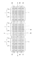
- FIG. 1 is a schematic plan view showing a solar cell according to an embodiment of the present invention. It is a typical top view which shows the state which affixed the tab on the solar cell in embodiment of this invention.
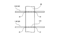
- FIG. 2 is a cross-sectional view taken along line A-A ′ of FIG. 1. It is a typical sectional view in an embodiment of the present invention. It is typical sectional drawing which shows the state which affixed the tab on the solar cell in embodiment of this invention. It is a typical top view which shows the state which affixed the tab on the solar cell in embodiment of this invention. It is a typical sectional view in an embodiment of the present invention.
- FIG. 1 shows a solar cell module according to this embodiment.
- the solar cell module includes a plurality of plate-like solar cells 1.
- the solar cell 1 is made of, for example, a crystalline semiconductor composed of single crystal silicon or polycrystalline silicon having a thickness of about 0.15 mm, and has a substantially square shape with a side of 125 mm. It is not limited to this, and solar cells with other configurations may be used.
- an n-type region and a p-type region are formed, and a semiconductor junction for forming an electric field for carrier separation at an interface portion between the n-type region and the p-type region is formed.
- the surface electrode 11 is formed on the light receiving surface (front surface) side surface of the solar cell 1, and the back electrode 12 is formed on the back surface side.
- the surface electrode 11 includes a plurality of finger electrodes 110 formed in parallel to each other. For example, about 55 finger electrodes 110 are formed with a finger electrode width of about 100 ⁇ m and a pitch of about 2 mm.
- a tab 20 as a wiring member is connected perpendicularly to the finger electrode 110.
- a bus bar electrode 111 is provided on the surface electrode 11 in accordance with a position where the tab 20 is connected. The bus bar electrode 111 is electrically connected to all the finger electrodes 110.
- the bus bar electrode 111 is formed in a polygonal line shape in order to improve adhesiveness with the tab 20 and electrical connection between the finger electrode 110 and the tab 20.
- a back surface electrode 12 is formed on the surface portion of the back surface side of the solar cell 1.
- the back surface electrode 12 includes a plurality of finger electrodes 120 formed in parallel to each other. For example, about 217 finger electrodes 120 with a finger electrode width of about 100 ⁇ m and a pitch of about 0.5 mm are formed.
- a bus bar electrode 121 is provided on the back electrode 12 in accordance with the position where the tab 20 is connected. The bus bar electrode 121 is electrically connected to all the finger electrodes 120.
- the bus bar electrode 112 is formed in a polygonal line shape in order to improve the adhesiveness with the tab 20 and the electrical connection between the finger electrode 120 and the tab 20.
- the front electrode 11 and the back electrode 12 can be formed by screen printing a thermosetting or heat-baked silver paste, for example.
- other methods such as a vapor deposition method, a sputtering method, or a plating method may be used.
- FIG. 2 in the region where the tabs 20 of the bus bar electrode 111 (121) and the finger electrode 110 (120) are connected, the points indicated in FIG. A region is schematically shown. Further, in FIG. 3, the points in the tab 20 also schematically show the regions where the crests bite into the electrodes. The tab 20 has such a thin width that the bending angle of the finger electrode 110 (120) is exposed. This facilitates the alignment between the tab 20 and the finger electrode 110 (120).
- three tabs 20 are connected on the front electrode 11 and the back electrode 12.
- the width a of the tab 20 is about 1.5 mm.
- the number of finger electrodes 110 of the front surface electrode 11 is made smaller than the number of finger electrodes 120 of the back surface electrode 12. Moreover, by making the thickness of the finger electrode 110 of the front electrode 11 larger than the thickness of the finger electrode 120 of the back electrode 12, the resistance of the front electrode 11 can be reduced, and further the solar cell characteristics can be improved. .
- FIGS. 1 and 4 are cross-sectional views taken along line A-A ′ of FIG.
- a tab 20 as a wiring member is electrically connected to the front electrode 11 and the back electrode 12.
- the resin agent 3 is used.
- the resin agent 3 for example, an anisotropic conductive resin agent is used.
- the anisotropic conductive resin agent includes at least a resin adhesive component and conductive particles dispersed therein.
- the resin adhesive component is composed of a composition containing a thermosetting resin.
- a thermosetting resin for example, an epoxy resin, a phenoxy resin, an acrylic resin, a polyimide resin, a polyamide resin, a polycarbonate resin, a urethane resin, or the like can be used.
- thermosetting resins are used singly or in combination of two or more, and one or more thermosetting resins selected from the group consisting of epoxy resins, phenoxy resins and acrylic resins are preferable.
- the conductive particles include metal particles such as gold particles, silver particles, copper particles, and nickel particles, or conductive or insulating core particles such as gold plating particles, copper plating particles, and nickel plating particles. Conductive particles formed by coating with a conductive layer such as a layer are used.
- the resin agent 3 is disposed between the front electrode 11 and the back electrode 12 of the solar cell 1 and the tab 20.
- the resin agent 3 is preferably the same as or slightly narrower than the width of the tab 20 to be connected.
- the width of the resin agent 3 is also 0.5 mm to 3 mm corresponding to the width of the tab 20 or slightly narrower than this.
- three tabs 20 having a width of 1.2 mm are used.
- the three resin agents 3 having a width corresponding to the width of the tab 20 are arranged on the position where the tab 20 is bonded.
- the resin agent 3 may be wider than the width of the tab 20 as long as it has translucency even after curing. *
- the tab 20 is composed of a copper thin plate 20 a as a core material, and a silver layer 20 b is provided on the surface of the tab 20.
- the silver layer 20 b constitutes a harder layer than the front electrode 11 and the back electrode 12.
- the tab 20 has at least one surface provided with fine unevenness, and the height of the uneven portion is about 10 to 50 ⁇ m.
- the tab 20 shown in FIG. 6 has fine irregularities on one side, and the opposite side is a flat surface. Such a tab is called a single-sided uneven tab.
- the tab 20 shown in FIG. 10 has fine irregularities on both sides. Such a tab 20 is referred to as a double-sided uneven tab.
- As the unevenness of the tab one having grooves formed in the longitudinal direction of the tab 20 or one having a large number of pyramidal protrusions formed on the surface can be used.
- the tab 20 provided with the silver layer 20b on the surface having the fine irregularities described above is pressed against the resin agent 3, and heat treatment is performed while pressing the resin agent 3 to thermally cure the tab 20 with the surface electrode 11 and the back electrode. 12 is connected.
- one end side of the tab 20 is connected to the surface electrode 11 on the light receiving surface side of the predetermined solar cell 1.
- the tabs 20 are respectively placed on the resin agents 3 arranged on the front and back of the solar cell 1 so that the other end side is connected to the back electrode 12 on the back side of another solar cell adjacent to the predetermined solar cell 1.
- the solar cell 1 is prepared ((a) in the figure), and the resin agent 3 is placed on the front electrode 11 and the back electrode 12 of the solar cell 1 ((b) in the figure). Then, for example, the solar cell 1 placed on the heat block 6 is pressed by using another heat block 6 at a pressure of, for example, about 0.05 to 1.00 MPa, and the tab 20 is moved through the resin agent 3 to the sun. Press each battery 1 side. Then, the temperature of the heat block 6 is heated at a high temperature at which the resin adhesive component of the resin agent 3 is thermally cured, for example, heated to a temperature of 120 ° C. or higher and 200 ° C. or lower to fix the tab 20 by pressure bonding. They are electrically connected and arranged ((d) in the figure).
- the solar cell 1 is heated while applying pressure from the upper part of the tab 20 arranged on the resin agent 3 toward the solar cell 1. During this heating, the surface region of the silver layer 20 b of the tab 20 is kept harder than the front electrode 11 and the back electrode 12.
- the crests (convex portions) of the tab 20 bite into the front electrode 11 and the back electrode 12, and the tab 20, the front electrode 11, and the back electrode 12. Are joined by the resin agent 3.
- the silver layer 20b having the crests has the electrodes (bus bar electrodes 111 and 121) in which the silver powder is mainly hardened with an epoxy resin bite into the front electrode 11 and the back electrode 12, respectively.
- the second solar cell 1 is placed on the tab 20 and lightly crimped, and bonded in the same procedure as described above to join a desired number of solar cells 1 to form a string.
- a solar cell module is formed.
- the warpage of the solar cell 1 is considered to occur because the tab 20 and the solar cell 1 have different linear expansion coefficients. Since such a warp is proportional to the temperature, if the temperature applied to the tab 20 and the solar cell 1 increases, the warp of the solar cell 1 tends to increase. Therefore, it can be said that adhesive bonding at a low temperature is the most effective means for reducing the warpage of the solar cell 1.
- the bonding means is the resin agent 3 that can be performed at a lower temperature than the alloy bonding by solder, the stress due to warpage of the front and back of the solar cell 1 can be further reduced, and the warpage is reduced. Can be suppressed.
- the resin agent 3 is adhered around the silver layer 20b of the tab 20 that has digged into the front electrode 11 and the back electrode 12, the adhesiveness of the tab 20 can be enhanced.
- the anisotropic conductive resin agent is exemplified as the resin agent 3, but the resin agent 3 may be one that does not include conductive particles.
- the resin agent 3 may be one that does not include conductive particles.
- electrical connection is performed by bringing a part of the surface of the front electrode 11 and the back electrode 12 into direct contact with the surface of the tab 20. Even in this case, since the silver layer 20b of the tab 20 bites into the front electrode 11 and the back electrode 12, sufficient electrical connection can be obtained.
- a light-transmitting material such as EVA is connected between the surface member made of glass and the back member made of a material such as a weather resistant film or glass or plastic. And sandwiching them with a sealing material sheet having properties. And a solar cell module is obtained by sealing the solar cell 1 with a sealing material between a surface member and a back surface member with a laminating apparatus.
- FIG. 11 shows a state in which the front and back surfaces of adjacent solar cells 1 are connected using a single-sided uneven tab.
- the peak portion faces the front surface side of the solar cell 1 and the flat portion faces the back surface side. Accordingly, the peak portion of the tab 20 on the surface side bites into the electrode 11. However, the tab 20 does not bite into the back electrode 12 on the back side of the solar cell 1.
- the front and back surfaces of two adjacent solar cells 1 are connected by a tab 20.
- the peak portion of the tab 20 can be bitten into both the front electrode 11 and the back electrode 12.
- two adjacent solar cells 1 are connected in parallel, and a pair of solar cells 1 connected in parallel are connected in series.
- FIG. 8 shows a state in which the front and back surfaces of adjacent solar cells 1 are connected using a double-sided uneven tab.
- the peak portion of the tab 20 faces both the front surface electrode 11 and the back surface electrode 12 of the solar cell 1. Therefore, as shown in FIG. 10, the crests of the tabs 20 on the front and back sides bite into the front electrode 11 and the back electrode 12, respectively.
- FIG. 9 shows that two front and back surfaces of two adjacent solar cells 1 are connected by a double-sided uneven tab.
- two adjacent solar cells 1 are connected in parallel, and a pair of solar cells 1 connected in parallel are connected in series.
- a solar cell module according to the present invention and a solar cell module of a reference example were prepared, and a temperature cycle test was performed.
- the temperature cycle test the temperature is changed from room temperature to 90 ⁇ 2 ° C. to ⁇ 40 ⁇ 3 ° C. to room temperature, and the temperature change rate is 87 ° C. / Performed every hour, this temperature cycle was performed 400 times.
- the reference example uses a copper foil 20a having a tin coating layer 20b on the surface as a soft conductor as a tab 20, and using the above-mentioned anisotropic conductive adhesive, the surface electrode 11, This is connected to the back electrode 12.
- the tab 20 coated with tin is not provided with irregularities.
- Example 1 of the present invention uses a single-sided uneven tab provided with a silver layer 20b on the surface side, and a tin coating layer 20b on the surface as a soft conductor on the copper foil 20a on the back side. It is provided.
- the corresponding tabs 20 are connected to the front and back of one solar cell 1, and the tab 20 is connected between a front surface member made of glass and a back surface member made of a weather-resistant film. And sandwiching them with a sealing material sheet having translucency. And a solar cell is sealed with the sealing material between the surface member and the back surface member by the laminating apparatus.
- Table 1 shows the rate of decrease based on the output values in the conventional example and Example 1.
- the rate of decrease was normalized with reference example 1. From Table 1, it can be seen that by causing the silver layer 20b of the tab 20 to bite into the surface electrode 11, the rate of decrease is greatly reduced to 0.44 even after 400 temperature cycles.
- Example 1 of the present invention As shown in Example 1 of the present invention and Example 2 in which the silver layer 20b is bitten into both the front surface electrode 11 and the back surface electrode 12 using the double-sided uneven tab 20 as shown in FIG. A temperature cycle test was conducted. The results are shown in Table 2.
- Example 1 The rate of decrease based on the output value in the example is shown.
- Example 1 was standardized as 1. From Table 2, it can be seen that when the double-sided uneven tab 20 is used, the reduction rate is 0.74 compared to that of the single-sided tab 20 even after 600 temperature cycles, which is more effective.
- the solar cell 1 in the present invention for example, a solar cell having a so-called HIT (registered trademark) structure in which an amorphous silicon layer is laminated on the surface of a crystalline silicon substrate, or a normal crystalline or thin film solar cell is used. be able to.
- HIT registered trademark
- the bus bar electrodes 111 and 121 are formed in a polygonal line shape, but the present invention can be applied even in a straight line shape.
- the electrodes are constituted by finger electrodes and bus bar electrodes, but the present invention can also be applied to solar cells having only finger electrodes as electrodes.
- the tab material is described as a copper foil.
- the tab material may be any material having a low electrical resistance, and may be iron, nickel, silver, or a mixture thereof. However, the same effect can be obtained.
- the tab is made of a material having a different core material and surface.
- the present invention can be applied even if the core material and the surface are the same material.
Abstract
【課題】 本発明は、温度サイクルにおいて配線部材の剥がれを抑制し、太陽電池出力を向上させることを目的とする。 【解決手段】 本発明は、隣接する太陽電池1の表面上に形成された表面電極11、裏面電極12をタブ20によって接続することにより、互いに接続された複数の太陽電池1を備える太陽電池モジュールであって、タブ20の一部は、表面電極11、裏面電極12の中に食い込み、太陽電池1とタブ20とは、樹脂剤3によって接着されていることを特徴とする。
Description
本発明は、太陽電池モジュール及び太陽電池モジュールの製造方法に関するものである。
太陽電池モジュールは、複数の太陽電池がその表裏面の電極に電気的に接続された配線部材により直列及び/又は並列に接続された構造を有している。太陽電池モジュールを作製する際に、太陽電池の電極と配線部材との接続には、従来、半田が用いられている。半田は、導通性、固着強度等の接続信頼性に優れ、安価で汎用性があることから広く用いられている。
一方、配線部材の接続時の熱影響を低減するため、太陽電池において半田を使用しない配線の接続方法も検討されている。例えば、樹脂接着剤を有する接着フィルムを用いて太陽電池と配線部材とを接続する方法が知られている(例えば、特許文献1参照)。
接着フィルムを用いた配線の接続は、接着フィルムを太陽電池の電極と配線部材との間に配置し、太陽電池と配線材とを相対的に加圧しつつ加熱することにより、樹脂接着剤により配線部材を太陽電池の電極に接続させている。
上記した樹脂接着剤を用いた太陽電池モジュールにおいて、電極と配線部材との間の剥がれを解消するために、太陽電池の表面上に形成されたバスバー電極を配線部材の中に埋め込むように構成したものが提案されている(例えば、特許文献2)。配線部材はバスバー電極が埋め込まれやすいように、銅箔の周囲に半田などの軟導電体層を設けている。
上記した特許文献2に記載された太陽電池モジュールにおいては、電極剥がれに対して十分な強度を有しているが、温度サイクルの信頼性において、更に信頼性を向上させることが望まれている。
本発明は、上記した要望に鑑み、温度サイクルにおいて配線部材の剥がれを抑制し、太陽電池出力を向上させることを目的とする。
本発明は、隣接する太陽電池の表面上に形成された電極を配線部材によって接続することにより、互いに接続された複数の太陽電池を備える太陽電池モジュールであって、前記配線部材の一部は、前記電極の中に食い込み、前記太陽電池と前記タブとは、樹脂によって接着されていることを特徴とする。
また、本発明は、太陽電池の表面上に電極を形成する工程と、前記電極を覆うように配置された樹脂上に、隣接する太陽電池の表面上に形成された電極と接続する配線部材を配置する工程と、前記配線部材上部から前記太陽電池の方向へ圧力をかけながら、当該太陽電池を加熱し、前記電極に配線部材の一部を食い込ませる工程と、を含み、前記配線部材の表面は前記電極の表面より硬いことを特徴とする。
本発明によれば、電極に配線部材の一部が食い込むことで、温度サイクルにおいてもタブ強度が保たれ、信頼性高い太陽電池モジュールが得られる。
本発明の実施の形態に係る太陽電池モジュールにつき図面を参照しながら詳細に説明する。なお、図中同一または相当部分には同一符号を付し、説明の重複を避けるためにその説明は繰返さない。
本図1は本実施形態にかかる太陽電池モジュールである。図1に示すように、太陽電池モジュールは、複数の板状の太陽電池1を備えている。太陽電池1は、例えば、厚みが0.15mm程度の単結晶シリコンや多結晶シリコンなどで構成される結晶系半導体からなり、1辺が125mmの略正方形を有するが、厚みや大きさ等はこれに限るものではなく、また、他構成の太陽電池を用いても良い。
太陽電池1内には、例えば、n型領域とp型領域が形成され、n型領域とp型領域との界面部分でキャリア分離用の電界を形成するための半導体接合部が形成されている。
図2に示すように、太陽電池1の受光面(表面)側の表面上には、表面電極11、裏面側の表面上には裏面電極12が形成されている。本実施形態において、表面電極11は、互いに平行に形成された複数のフィンガー電極110からなる。フィンガー電極110は、例えば、フィンガー電極幅約100μm、ピッチ約2mmで55本程度形成される。図3に示すように、フィンガー電極110に直交して配線部材としてのタブ20が接続される。表面電極11には、タブ20が接続される位置に合わせてバスバー電極111が設けられている。バスバー電極111は全てのフィンガー電極110と電気的に接続されている。バスバー電極111は、タブ20との接着性並びにフィンガー電極110とタブ20との電気的接続を良好にするために、折れ線状に形成されている。
また、太陽電池1の裏面側の表面部分には、裏面電極12が形成されている。裏面電極12は、互いに平行に形成された複数のフィンガー電極120からなる。フィンガー電極120は、例えば、フィンガー電極幅約100μm、ピッチ約0.5mmで217本程度形成される。裏面電極12には、タブ20が接続される位置に合わせてバスバー電極121が設けられている。バスバー電極121は全てのフィンガー電極120と電気的に接続されている。バスバー電極112は、タブ20との接着性並びにフィンガー電極120とタブ20との電気的接続を良好にするために、折れ線状に形成されている。
このような表面電極11及び裏面電極12は、例えば、熱硬化型或いは熱焼成型の銀ペーストをスクリーン印刷することによって形成することができる。また、これ以外に蒸着法やスパッタ法或いはメッキ法等他の方法を用いて形成しても良い。
図2において、バスバー電極111(121)及びフィンガー電極110(120)のタブ20が接続される領域において、点々で記載しているのは、後述するように、タブ20の山部が電極に食い込む領域を模式的に示している。また、図3において、タブ20の中の点々も山部が電極に食い込む領域を模式的に示している。タブ20は、フィンガー電極110(120)の折れ曲がり角が露出する程度の細い幅となる。これによって、タブ20とフィンガー電極110(120)との位置合わせが容易になる。
図1に示すように、表面電極11上、裏面電極12上に、3本のタブ20が接続される。タブ20の幅aは約1.5mmである。
尚、太陽電池1の受光面に入射する光の量を増大させるために、表面電極11のフィンガー電極110の本数を、裏面電極12のフィンガー電極120の本数より少なくしている。また、表面電極11のフィンガー電極110の厚みを、裏面電極12のフィンガー電極120の厚みより大きくすることで、表面電極11の抵抗を小さくすることができ、さらに太陽電池特性を向上させることができる。
次に、上記した太陽電池1を用いて太陽電池モジュールを製造する方法につき説明する。図4は、図1のA-A’線断面図である。太陽電池モジュールは、図1、図4に示すように、表面電極11、裏面電極12に配線部材としてのタブ20が電気的に接続される。タブ20を表面電極11、裏面電極12に接続するために樹脂剤3が用いられる。樹脂剤3としては、例えば、異方性導電樹脂剤が用いられる。
異方性導電樹脂剤としては、樹脂接着成分とその中に分散した導電性粒子とを少なくとも含んで構成されている。樹脂接着成分は熱硬化性樹脂を含有する組成物からなり、例えば、エポキシ樹脂、フェノキシ樹脂、アクリル樹脂、ポリイミド樹脂、ポリアミド樹脂、ポリカーボネート樹脂、ウレタン樹脂等を用いることができる。これらの熱硬化性樹脂は、1種を単独で用いるか2種以上を組み合わせて用いられ、エポキシ樹脂、フェノキシ樹脂及びアクリル樹脂からなる群より選ばれる1種以上の熱硬化性樹脂が好ましい。
導電性粒子としては、例えば、金粒子、銀粒子、銅粒子及びニッケル粒子などの金属粒子、或いは、金メッキ粒子、銅メッキ粒子及びニッケルメッキ粒子などの導電性又は絶縁性の核粒子の表面を金属層などの導電層で被覆してなる導電性粒子が用いられる。
まず、太陽電池1の表面電極11及び裏面電極12とタブ20との間に、樹脂剤3を配置する。樹脂剤3は、接続するタブ20の幅と同一若しくは少し幅の細いものが好ましい。例えば、タブ20の幅が、0.5mm~3mmであれば、樹脂剤3の幅もタブ20の幅に対応して0.5mm~3mm若しくはこれより少し幅の細いものにする。本実施形態においては、図1に示すように、幅1.2mmの3本のタブ20を用いている。このため、タブ20が接着される位置上にタブ20の幅に対応した幅の3本の樹脂剤3が配置される。尚、樹脂剤3は、硬化後も透光性を有するものであれば、タブ20の幅より広くても良い。
図6に示すように、タブ20は、芯材としての銅薄板20aで構成され、タブ20の表面には、銀層20bを設けている。銀層20bは、表面電極11、裏面電極12より硬い層を構成している。
タブ20としては、少なくとも片面に微細な凹凸が設けられ凹凸の山部の高さ約10~50μmである。図6に示すタブ20は、片面に微細な凹凸が設けられ、反対面は平坦な面である。このようなタブを片面凹凸タブという。図10に示すタブ20は、両面に微細な凹凸が設けられている。このようなタブ20を両面凹凸タブという。タブの凹凸としては、タブ20の長手方向に溝を形成したものや、ピラミッド状の凸部を多数表面上に形成したもの等を用いることができる。
上記した微細な凹凸を有する表面に銀層20bを設けたタブ20を樹脂剤3に押圧し、押圧しながら加熱処理を施して樹脂剤3を熱硬化してタブ20を表面電極11、裏面電極12に接続する。
複数の太陽電池1の各々を互いに隣接する他の太陽電池1とタブ20によって電気的に接続するには、タブ20の一方端側が所定の太陽電池1の受光面側の表面電極11に接続されるとともに、他方端側がその所定の太陽電池1に隣接する別の太陽電池の裏面側の裏面電極12に接続するように、太陽電池1の表裏に配置した樹脂剤3にそれぞれタブ20を置く。
図13に示すように、太陽電池1を用意し(図中(a))、太陽電池1の表面電極11、裏面電極12に樹脂剤3を載せる(図中(b))。そして、例えば、ヒートブロック6上に載せられた太陽電池1を例えば、0.05~1.00MPa程度の圧力で他のヒートブロック6を用いて押圧し、樹脂剤3を介してタブ20を太陽電池1側にそれぞれ押し付ける。そして、ヒートブロック6の温度を樹脂剤3の樹脂接着成分が熱硬化する温度での高温加熱、例えば、120℃以上200℃以下の温度に加熱してタブ20を圧着固定させ、太陽電池1を電気的に接続して配列する(図中(d))。
樹脂剤3上に配置されたタブ20上部から太陽電池1の方向へ圧力をかけながら、当該太陽電池1を加熱する。この加熱時において、タブ20の銀層20bの表面領域は、表面電極11、裏面電極12よりも硬い状態が保たれる。
そうすると、図6、図7及び図13(d)に示すように、表面電極11、裏面電極12内に、タブ20の山部(凸部)が食い込み、タブ20と表面電極11、裏面電極12とが樹脂剤3にて接合される。このように、山部を有する銀層20bが、銀粉末を主としてエポキシ樹脂で固められた電極(バスバー電極111、121)がそれぞれ表面電極11、裏面電極12に食い込む。
同様にして、2枚目の太陽電池1をタブ20上に重ね置いて軽く圧着し、上述した同様の手順で接着を行い、所望する枚数の太陽電池1を接合していき、ストリングが形成され、太陽電池モジュールが形成される。
太陽電池1の反りは、タブ20と太陽電池1との線膨張係数が異なるために発生すると考えられる。このような反りは温度に比例することから、タブ20と太陽電池1とに加える温度が高くなれば、太陽電池1の反りは大きくなりやすい。従って、太陽電池1の反りの低減には、低い温度での接着接合が最も有効な手段といえる。
本実施形態に係る太陽電池モジュールによると、接着手段を半田による合金接合よりも低温で行うことができる樹脂剤3にしたため、太陽電池1の表裏の反りによる応力をより小さくすることができ、反りの発生を抑えることができる。
更に、樹脂剤3が表面電極11、裏面電極12に食い込んだタブ20の銀層20bの周辺で接着しているので、タブ20の接着性を高めることができる。
なお、上記した実施形態では、樹脂剤3として異方性導電樹脂剤を例示したが、樹脂剤3としては導電性粒子を含まないものも用いることができる。樹脂剤3として導電性粒子を含まない樹脂剤を用いる場合には、表面電極11及び裏面電極12の表面の一部をタブ20の表面に直接接触させることによって、電気的な接続を行う。この場合においてもタブ20の銀層20bが表面電極11、裏面電極12に食い込んでいるので、十分な電気的接続が得られる。
このようにして、タブ20により複数の太陽電池1を接続したものを、ガラスからなる表面部材と耐侯性フィルム又はガラス、プラスチックのような部材からなる裏面部材との間に、EVA等の透光性を有する封止材シートで挟んで重ね合わせる。そして、ラミネート装置により、太陽電池1を表面部材と裏面部材との間に封止材により封止することにより、太陽電池モジュールが得られる。
図11は、片面凹凸タブを用いて隣り合う太陽電池1の表面と裏面とを接続した状態を示している。この例では、太陽電池1の表面側に山部が面し、裏面側には平坦部が面することになる。従って、表面側のタブ20の山部が電極11に食い込む。但し太陽電池1の裏面側では、タブ20は裏面電極12には食い込まない。
図5は、隣り合う2つの太陽電池1の表面同士、裏面同士をタブ20で接続している。この例では、片面凹凸タブを用いても表面電極11、裏面電極12の両方にタブ20の山部を食い込ませることができる。この例では隣り合う2つの太陽電池1が並列に接続され、並列に接続された一対の太陽電池1同士を直列に接続している。
図8は、両面凹凸タブを用いて隣り合う太陽電池1の表面と裏面とを接続した状態を示している。この例では、太陽電池1の表面電極11、裏面電極12の両方にタブ20の山部が面することになる。従って、図10に示すように、表裏面側のタブ20の山部が表面電極11、裏面電極12にそれぞれ食い込んでいる。
図9は、隣り合う2つの太陽電池1の表面同士、裏面同士を両面凹凸タブで接続している。この例では隣り合う2つの太陽電池1が並列に接続され、並列に接続された一対の太陽電池1同士を直列に接続している。
次に、本発明による太陽電池モジュールと参考例の太陽電池モジュールを用意し、温度サイクル試験を行った。温度サイクル試験は、温度を常温から90±2℃から-40±3℃から常温に変化させ、各上下限10分以上、1サイクル6時間以下で、温度変化率は上昇、下降ともに87℃/毎時で行い、この温度サイクルを400回行った。参考例は、図12に示すように、銅箔20aに軟導体として表面に錫のコーティング層20bを設けたものをタブ20として用い、上記した異方性導電接着剤を用いて表面電極11、裏面電極12に接続したものである。尚、錫をコーティングしたタブ20には凹凸は設けていない。本発明の実施例1は、図11に示すように、表面側は、銀層20bを設けた片面凹凸タブを用い、裏面側は、銅箔20aに軟導体として表面に錫のコーティング層20bを設けたものである。
この実験に用いた太陽電池モジュールは、1枚の太陽電池1の表裏にそれぞれ該当するタブ20を接続し、それをガラスからなる表面部材と耐侯性フィルムからなる裏面部材との間に、EVA等の透光性を有する封止材シートで挟んで重ね合わせる。そして、ラミネート装置により、太陽電池を表面部材と裏面部材との間に封止材により封止したものである。
400回の温度サイクル試験を行った結果を表1に示す。

表1は、従来例及び実施例1における出力値を基準とした低下率を示す。尚、低下率は、参考例を1として規格化した。表1から、タブ20の銀層20bを表面電極11に食い込ませることにより、温度サイクルの400回後においても低下率が0.44と大幅に減っているのが分かる。
次に、本発明の実施例1と図10に示すように両面凹凸タブ20を用いて両方の表面電極11、裏面電極12に銀層20bを食い込ませた実施例2を用意し、600回の温度サイクル試験を行った。その結果を表2に示す。
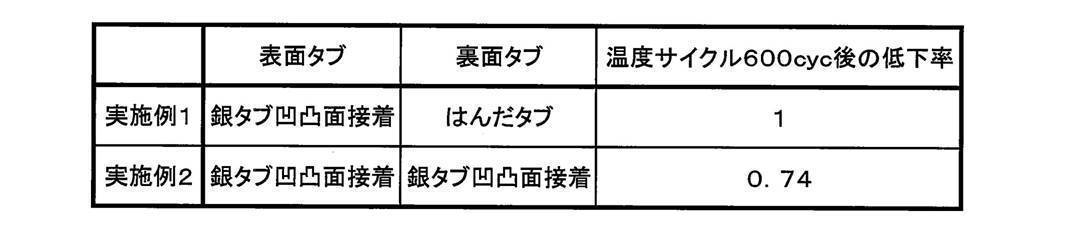
実施例における出力値を基準とした低下率を示す。尚、実施例1を1として規格化した。表2より、両面凹凸のタブ20を用いると、600回の温度サイクル後においても、片面タブ20のものに比して0.74の低下率であり、より効果があることが分かる。
上記したように、本発明は、タブが太陽電池の表面電極又は裏面電極に食い込むことにより、アンカー効果が生じ、タブの熱膨張、熱収縮の際のタブの動きが抑制され、温度変化に対する信頼性が高まったと考えられる。
本発明における太陽電池1としては、例えば、結晶系シリコン基板表面に非晶質シリコン層を積層したいわゆるHIT(登録商標)構造を有する太陽電池や通常の結晶系あるいは薄膜系の太陽電池をもちいることができる。
また、上記した実施形態は、バスバー電極111、121として折れ線状に形成されているが、直線状であっても本発明は適用できる。
また、上記した実施形態は、電極はフィンガー電極とバスバー電極で構成しているが、電極としてフィンガー電極のみを有する太陽電池においても本発明は適用できる。
又、本実施形態において、タブの材料を銅箔として説明を行ったが、タブの材料としては電気抵抗が小さいものであればよく、他に鉄、ニッケル、銀あるいはこれらを混合したものであっても、同様な効果が得られる。
更に、本実施形態において、タブは、芯材と表面とが異なる材料で構成されていたが、芯材と表面とが同じ材料であっても本発明は適用できる。
今回開示された実施の形態はすべての点で例示であって制限的なものではないと考えられるべきである。本発明の範囲は、上記した実施の形態の説明ではなくて特許請求の範囲によって示され、特許請求の範囲と均等の意味および範囲内でのすべての変更が含まれることが意図される。
1 太陽電池
3 樹脂層
11 表面電極
12 裏面電極
20 タブ
20a 銅箔
20b 銀層
3 樹脂層
11 表面電極
12 裏面電極
20 タブ
20a 銅箔
20b 銀層
Claims (4)
- 隣接する太陽電池の表面上に形成された電極を配線部材によって接続することにより、
互いに接続された複数の太陽電池を備える太陽電池モジュールであって、
前記配線部材の一部は、前記電極の中に食い込み、
前記太陽電池と前記配線部材とは、樹脂によって接着されていることを特徴とする太陽電池モジュール。 - 前記配線部材は、少なくとも片面に前記電極の表面より硬い凹凸が形成されていることを特徴とする請求項1に記載の太陽電池モジュール。
- 太陽電池の表面上に電極を形成する工程と、
前記電極を覆うように配置された樹脂上に、隣接する太陽電池の表面上に形成された電極と接続する配線部材を配置する工程と、
前記配線部材上部から前記太陽電池の方向へ圧力をかけながら、当該太陽電池を加熱し、前記電極に配線部材の一部を食い込ませる工程と、を含み、前記配線部材の表面は前記電極の表面より硬いことを特徴とする太陽電池モジュールの製造方法。 - 前記配線部材は、少なくとも片面に凹凸が形成されていることを特徴とする請求項3に記載の太陽電池モジュールの製造方法。
Priority Applications (3)
| Application Number | Priority Date | Filing Date | Title |
|---|---|---|---|
| JP2012518367A JP5991534B2 (ja) | 2010-05-31 | 2011-05-27 | 太陽電池モジュール及び太陽電池モジュールの製造方法 |
| EP11789722.3A EP2579332B1 (en) | 2010-05-31 | 2011-05-27 | Solar cell module and solar cell module manufacturing method |
| US13/683,131 US8927851B2 (en) | 2010-05-31 | 2012-11-21 | Solar cell module and method of manufacturing solar cell module |
Applications Claiming Priority (2)
| Application Number | Priority Date | Filing Date | Title |
|---|---|---|---|
| JP2010125230 | 2010-05-31 | ||
| JP2010-125230 | 2010-05-31 |
Related Child Applications (1)
| Application Number | Title | Priority Date | Filing Date |
|---|---|---|---|
| US13/683,131 Continuation US8927851B2 (en) | 2010-05-31 | 2012-11-21 | Solar cell module and method of manufacturing solar cell module |
Publications (1)
| Publication Number | Publication Date |
|---|---|
| WO2011152319A1 true WO2011152319A1 (ja) | 2011-12-08 |
Family
ID=45066686
Family Applications (1)
| Application Number | Title | Priority Date | Filing Date |
|---|---|---|---|
| PCT/JP2011/062259 WO2011152319A1 (ja) | 2010-05-31 | 2011-05-27 | 太陽電池モジュール及び太陽電池モジュールの製造方法 |
Country Status (4)
| Country | Link |
|---|---|
| US (1) | US8927851B2 (ja) |
| EP (1) | EP2579332B1 (ja) |
| JP (2) | JP5991534B2 (ja) |
| WO (1) | WO2011152319A1 (ja) |
Cited By (3)
| Publication number | Priority date | Publication date | Assignee | Title |
|---|---|---|---|---|
| US9040813B2 (en) | 2012-02-23 | 2015-05-26 | Lg Electronics Inc. | Solar cell module |
| JP2016006819A (ja) * | 2014-06-20 | 2016-01-14 | 日立化成株式会社 | 太陽電池モジュールの製造方法 |
| US20160064587A1 (en) * | 2013-04-25 | 2016-03-03 | Panasonic Intellectual Property Management Co., Ltd. | Solar cell module and method for manufacturing solar cell module |
Families Citing this family (4)
| Publication number | Priority date | Publication date | Assignee | Title |
|---|---|---|---|---|
| US10000645B2 (en) | 2015-11-24 | 2018-06-19 | PLANT PV, Inc. | Methods of forming solar cells with fired multilayer film stacks |
| WO2017091782A1 (en) * | 2015-11-24 | 2017-06-01 | Plant Pv, Inc | Fired multilayer stacks for use in integrated circuits and solar cells |
| WO2017179523A1 (ja) * | 2016-04-14 | 2017-10-19 | 株式会社カネカ | 太陽電池用配線材および太陽電池モジュール |
| US11575053B2 (en) * | 2017-05-10 | 2023-02-07 | Sharp Kabushiki Kaisha | Photovoltaic device and solar cell module including same |
Citations (5)
| Publication number | Priority date | Publication date | Assignee | Title |
|---|---|---|---|---|
| JP2006278710A (ja) * | 2005-03-29 | 2006-10-12 | Kyocera Corp | 太陽電池モジュール及びその製造方法 |
| JP2007214533A (ja) | 2006-01-16 | 2007-08-23 | Hitachi Chem Co Ltd | 導電性接着フィルム及び太陽電池モジュール |
| WO2008023795A1 (en) | 2006-08-25 | 2008-02-28 | Sanyo Electric Co., Ltd. | Solar battery module and solar battery module manufacturing method |
| WO2009104627A1 (ja) * | 2008-02-21 | 2009-08-27 | 三洋電機株式会社 | 太陽電池モジュール |
| WO2009144898A1 (ja) * | 2008-05-27 | 2009-12-03 | 株式会社フジクラ | 光電変換素子 |
Family Cites Families (8)
| Publication number | Priority date | Publication date | Assignee | Title |
|---|---|---|---|---|
| US4301322A (en) * | 1980-04-03 | 1981-11-17 | Exxon Research & Engineering Co. | Solar cell with corrugated bus |
| JP3319697B2 (ja) * | 1996-11-29 | 2002-09-03 | 太陽誘電株式会社 | 巻線型電子部品及びその製造方法 |
| US6586270B2 (en) * | 2000-06-01 | 2003-07-01 | Canon Kabushiki Kaisha | Process for producing a photovoltaic element |
| US7476800B2 (en) * | 2005-06-01 | 2009-01-13 | Outokumpu Copper Neumayer Gmbh | Electric connection element |
| JP4294048B2 (ja) * | 2006-11-29 | 2009-07-08 | 三洋電機株式会社 | 太陽電池モジュール |
| CN101675484B (zh) * | 2007-05-09 | 2012-07-04 | 日立化成工业株式会社 | 导电体连接用部件、连接结构和太阳能电池组件 |
| KR101248636B1 (ko) * | 2007-05-09 | 2013-04-01 | 히타치가세이가부시끼가이샤 | 도전체의 접속 방법, 도전체 접속용 부재, 접속 구조 및 태양 전지 모듈 |
| WO2009041506A1 (ja) * | 2007-09-26 | 2009-04-02 | Hitachi Chemical Company, Ltd. | 導電体接続用部材及びその製造方法、接続構造、並びに、太陽電池モジュール |
-
2011
- 2011-05-27 EP EP11789722.3A patent/EP2579332B1/en active Active
- 2011-05-27 JP JP2012518367A patent/JP5991534B2/ja not_active Expired - Fee Related
- 2011-05-27 WO PCT/JP2011/062259 patent/WO2011152319A1/ja active Application Filing
-
2012
- 2012-11-21 US US13/683,131 patent/US8927851B2/en not_active Expired - Fee Related
-
2015
- 2015-09-29 JP JP2015190655A patent/JP6043971B2/ja not_active Expired - Fee Related
Patent Citations (5)
| Publication number | Priority date | Publication date | Assignee | Title |
|---|---|---|---|---|
| JP2006278710A (ja) * | 2005-03-29 | 2006-10-12 | Kyocera Corp | 太陽電池モジュール及びその製造方法 |
| JP2007214533A (ja) | 2006-01-16 | 2007-08-23 | Hitachi Chem Co Ltd | 導電性接着フィルム及び太陽電池モジュール |
| WO2008023795A1 (en) | 2006-08-25 | 2008-02-28 | Sanyo Electric Co., Ltd. | Solar battery module and solar battery module manufacturing method |
| WO2009104627A1 (ja) * | 2008-02-21 | 2009-08-27 | 三洋電機株式会社 | 太陽電池モジュール |
| WO2009144898A1 (ja) * | 2008-05-27 | 2009-12-03 | 株式会社フジクラ | 光電変換素子 |
Non-Patent Citations (1)
| Title |
|---|
| See also references of EP2579332A4 |
Cited By (4)
| Publication number | Priority date | Publication date | Assignee | Title |
|---|---|---|---|---|
| US9040813B2 (en) | 2012-02-23 | 2015-05-26 | Lg Electronics Inc. | Solar cell module |
| US9496440B2 (en) | 2012-02-23 | 2016-11-15 | Lg Electronics Inc. | Solar cell module |
| US20160064587A1 (en) * | 2013-04-25 | 2016-03-03 | Panasonic Intellectual Property Management Co., Ltd. | Solar cell module and method for manufacturing solar cell module |
| JP2016006819A (ja) * | 2014-06-20 | 2016-01-14 | 日立化成株式会社 | 太陽電池モジュールの製造方法 |
Also Published As
| Publication number | Publication date |
|---|---|
| JP2016006913A (ja) | 2016-01-14 |
| JP5991534B2 (ja) | 2016-09-14 |
| JPWO2011152319A1 (ja) | 2013-08-01 |
| EP2579332A1 (en) | 2013-04-10 |
| US8927851B2 (en) | 2015-01-06 |
| US20130125951A1 (en) | 2013-05-23 |
| EP2579332A4 (en) | 2017-10-25 |
| JP6043971B2 (ja) | 2016-12-14 |
| EP2579332B1 (en) | 2021-02-17 |
Similar Documents
| Publication | Publication Date | Title |
|---|---|---|
| US10896984B2 (en) | Solar cell module | |
| JP6043971B2 (ja) | 太陽電池モジュール及び太陽電池モジュールの製造方法 | |
| JP5380810B2 (ja) | 太陽電池モジュール | |
| US20100243024A1 (en) | Solar cell, solar cell module and solar cell system | |
| US20120240985A1 (en) | Solar cell string and solar cell module using same | |
| JP5877604B2 (ja) | 太陽電池モジュールの製造方法、太陽電池モジュール及びタブ線の接続方法 | |
| JP5046743B2 (ja) | 太陽電池モジュール及びその製造方法 | |
| WO2008023795A1 (en) | Solar battery module and solar battery module manufacturing method | |
| JP2009295940A (ja) | 太陽電池セルおよび太陽電池モジュール | |
| WO2009104627A1 (ja) | 太陽電池モジュール | |
| JP5923732B2 (ja) | 太陽電池モジュール | |
| JP2012084560A (ja) | 結晶系太陽電池モジュール | |
| JP5545569B2 (ja) | 太陽電池用バックシートの製造方法 | |
| EP2579318A1 (en) | Photovoltaic cell module and photovoltaic cell | |
| WO2015037213A1 (ja) | 太陽電池セル、太陽電池モジュール及びその製造方法 | |
| JP5652911B2 (ja) | 太陽電池モジュールの製造方法 | |
| WO2013154188A1 (ja) | 太陽電池セル | |
| WO2017043518A1 (ja) | 太陽電池モジュールの製造方法、太陽電池モジュール、及び太陽電池セルの接続方法 | |
| TW201947869A (zh) | 太陽能電池串及其製造方法 | |
| JP2011108982A (ja) | 太陽電池モジュール | |
| JP2017175016A (ja) | 太陽電池モジュールの製造方法、太陽電池モジュール、太陽電池セルの接続方法、及び積層体 | |
| JP2011151246A (ja) | 太陽電池モジュールの製造方法 | |
| JP2015012117A (ja) | 太陽電池モジュール及びその製造方法 | |
| JP2017120810A (ja) | 太陽電池セル及び太陽電池モジュール |
Legal Events
| Date | Code | Title | Description |
|---|---|---|---|
| 121 | Ep: the epo has been informed by wipo that ep was designated in this application |
Ref document number: 11789722 Country of ref document: EP Kind code of ref document: A1 |
|
| WWE | Wipo information: entry into national phase |
Ref document number: 2012518367 Country of ref document: JP |
|
| NENP | Non-entry into the national phase |
Ref country code: DE |
|
| WWE | Wipo information: entry into national phase |
Ref document number: 2011789722 Country of ref document: EP |