WO2011135731A1 - 基板処理装置及び薄膜の製造方法 - Google Patents
基板処理装置及び薄膜の製造方法 Download PDFInfo
- Publication number
- WO2011135731A1 WO2011135731A1 PCT/JP2010/057919 JP2010057919W WO2011135731A1 WO 2011135731 A1 WO2011135731 A1 WO 2011135731A1 JP 2010057919 W JP2010057919 W JP 2010057919W WO 2011135731 A1 WO2011135731 A1 WO 2011135731A1
- Authority
- WO
- WIPO (PCT)
- Prior art keywords
- substrate
- chamber
- film
- air
- baking
- Prior art date
Links
Images


Classifications
-
- H—ELECTRICITY
- H01—ELECTRIC ELEMENTS
- H01L—SEMICONDUCTOR DEVICES NOT COVERED BY CLASS H10
- H01L21/00—Processes or apparatus adapted for the manufacture or treatment of semiconductor or solid state devices or of parts thereof
- H01L21/67—Apparatus specially adapted for handling semiconductor or electric solid state devices during manufacture or treatment thereof; Apparatus specially adapted for handling wafers during manufacture or treatment of semiconductor or electric solid state devices or components ; Apparatus not specifically provided for elsewhere
- H01L21/67005—Apparatus not specifically provided for elsewhere
- H01L21/67011—Apparatus for manufacture or treatment
- H01L21/67017—Apparatus for fluid treatment
-
- B—PERFORMING OPERATIONS; TRANSPORTING
- B05—SPRAYING OR ATOMISING IN GENERAL; APPLYING FLUENT MATERIALS TO SURFACES, IN GENERAL
- B05C—APPARATUS FOR APPLYING FLUENT MATERIALS TO SURFACES, IN GENERAL
- B05C11/00—Component parts, details or accessories not specifically provided for in groups B05C1/00 - B05C9/00
- B05C11/02—Apparatus for spreading or distributing liquids or other fluent materials already applied to a surface ; Controlling means therefor; Control of the thickness of a coating by spreading or distributing liquids or other fluent materials already applied to the coated surface
- B05C11/023—Apparatus for spreading or distributing liquids or other fluent materials already applied to a surface
-
- B—PERFORMING OPERATIONS; TRANSPORTING
- B05—SPRAYING OR ATOMISING IN GENERAL; APPLYING FLUENT MATERIALS TO SURFACES, IN GENERAL
- B05C—APPARATUS FOR APPLYING FLUENT MATERIALS TO SURFACES, IN GENERAL
- B05C11/00—Component parts, details or accessories not specifically provided for in groups B05C1/00 - B05C9/00
- B05C11/02—Apparatus for spreading or distributing liquids or other fluent materials already applied to a surface ; Controlling means therefor; Control of the thickness of a coating by spreading or distributing liquids or other fluent materials already applied to the coated surface
- B05C11/08—Spreading liquid or other fluent material by manipulating the work, e.g. tilting
-
- H—ELECTRICITY
- H01—ELECTRIC ELEMENTS
- H01L—SEMICONDUCTOR DEVICES NOT COVERED BY CLASS H10
- H01L21/00—Processes or apparatus adapted for the manufacture or treatment of semiconductor or solid state devices or of parts thereof
- H01L21/02—Manufacture or treatment of semiconductor devices or of parts thereof
- H01L21/02104—Forming layers
- H01L21/02107—Forming insulating materials on a substrate
- H01L21/02109—Forming insulating materials on a substrate characterised by the type of layer, e.g. type of material, porous/non-porous, pre-cursors, mixtures or laminates
- H01L21/02112—Forming insulating materials on a substrate characterised by the type of layer, e.g. type of material, porous/non-porous, pre-cursors, mixtures or laminates characterised by the material of the layer
- H01L21/02172—Forming insulating materials on a substrate characterised by the type of layer, e.g. type of material, porous/non-porous, pre-cursors, mixtures or laminates characterised by the material of the layer the material containing at least one metal element, e.g. metal oxides, metal nitrides, metal oxynitrides or metal carbides
- H01L21/02197—Forming insulating materials on a substrate characterised by the type of layer, e.g. type of material, porous/non-porous, pre-cursors, mixtures or laminates characterised by the material of the layer the material containing at least one metal element, e.g. metal oxides, metal nitrides, metal oxynitrides or metal carbides the material having a perovskite structure, e.g. BaTiO3
-
- H—ELECTRICITY
- H01—ELECTRIC ELEMENTS
- H01L—SEMICONDUCTOR DEVICES NOT COVERED BY CLASS H10
- H01L21/00—Processes or apparatus adapted for the manufacture or treatment of semiconductor or solid state devices or of parts thereof
- H01L21/02—Manufacture or treatment of semiconductor devices or of parts thereof
- H01L21/02104—Forming layers
- H01L21/02107—Forming insulating materials on a substrate
- H01L21/02225—Forming insulating materials on a substrate characterised by the process for the formation of the insulating layer
- H01L21/0226—Forming insulating materials on a substrate characterised by the process for the formation of the insulating layer formation by a deposition process
- H01L21/02282—Forming insulating materials on a substrate characterised by the process for the formation of the insulating layer formation by a deposition process liquid deposition, e.g. spin-coating, sol-gel techniques, spray coating
-
- H—ELECTRICITY
- H01—ELECTRIC ELEMENTS
- H01L—SEMICONDUCTOR DEVICES NOT COVERED BY CLASS H10
- H01L21/00—Processes or apparatus adapted for the manufacture or treatment of semiconductor or solid state devices or of parts thereof
- H01L21/67—Apparatus specially adapted for handling semiconductor or electric solid state devices during manufacture or treatment thereof; Apparatus specially adapted for handling wafers during manufacture or treatment of semiconductor or electric solid state devices or components ; Apparatus not specifically provided for elsewhere
- H01L21/67005—Apparatus not specifically provided for elsewhere
- H01L21/67011—Apparatus for manufacture or treatment
- H01L21/6715—Apparatus for applying a liquid, a resin, an ink or the like
-
- H—ELECTRICITY
- H01—ELECTRIC ELEMENTS
- H01L—SEMICONDUCTOR DEVICES NOT COVERED BY CLASS H10
- H01L21/00—Processes or apparatus adapted for the manufacture or treatment of semiconductor or solid state devices or of parts thereof
- H01L21/67—Apparatus specially adapted for handling semiconductor or electric solid state devices during manufacture or treatment thereof; Apparatus specially adapted for handling wafers during manufacture or treatment of semiconductor or electric solid state devices or components ; Apparatus not specifically provided for elsewhere
- H01L21/67005—Apparatus not specifically provided for elsewhere
- H01L21/67011—Apparatus for manufacture or treatment
- H01L21/67155—Apparatus for manufacturing or treating in a plurality of work-stations
- H01L21/67196—Apparatus for manufacturing or treating in a plurality of work-stations characterized by the construction of the transfer chamber
-
- H—ELECTRICITY
- H01—ELECTRIC ELEMENTS
- H01L—SEMICONDUCTOR DEVICES NOT COVERED BY CLASS H10
- H01L21/00—Processes or apparatus adapted for the manufacture or treatment of semiconductor or solid state devices or of parts thereof
- H01L21/67—Apparatus specially adapted for handling semiconductor or electric solid state devices during manufacture or treatment thereof; Apparatus specially adapted for handling wafers during manufacture or treatment of semiconductor or electric solid state devices or components ; Apparatus not specifically provided for elsewhere
- H01L21/67005—Apparatus not specifically provided for elsewhere
- H01L21/67011—Apparatus for manufacture or treatment
- H01L21/67155—Apparatus for manufacturing or treating in a plurality of work-stations
- H01L21/67207—Apparatus for manufacturing or treating in a plurality of work-stations comprising a chamber adapted to a particular process
-
- B—PERFORMING OPERATIONS; TRANSPORTING
- B05—SPRAYING OR ATOMISING IN GENERAL; APPLYING FLUENT MATERIALS TO SURFACES, IN GENERAL
- B05D—PROCESSES FOR APPLYING FLUENT MATERIALS TO SURFACES, IN GENERAL
- B05D1/00—Processes for applying liquids or other fluent materials
- B05D1/002—Processes for applying liquids or other fluent materials the substrate being rotated
- B05D1/005—Spin coating
-
- B—PERFORMING OPERATIONS; TRANSPORTING
- B05—SPRAYING OR ATOMISING IN GENERAL; APPLYING FLUENT MATERIALS TO SURFACES, IN GENERAL
- B05D—PROCESSES FOR APPLYING FLUENT MATERIALS TO SURFACES, IN GENERAL
- B05D3/00—Pretreatment of surfaces to which liquids or other fluent materials are to be applied; After-treatment of applied coatings, e.g. intermediate treating of an applied coating preparatory to subsequent applications of liquids or other fluent materials
- B05D3/04—Pretreatment of surfaces to which liquids or other fluent materials are to be applied; After-treatment of applied coatings, e.g. intermediate treating of an applied coating preparatory to subsequent applications of liquids or other fluent materials by exposure to gases
- B05D3/0486—Operating the coating or treatment in a controlled atmosphere
Definitions
- the present invention relates to a substrate processing apparatus provided with a spin coater and a method for manufacturing a thin film using the substrate processing apparatus.
- a conventional method for manufacturing a PZT film will be described.
- a (111) -oriented Pt film is formed on a 4-inch wafer, and a PZT sol-gel solution is spin-coated on the Pt film by a spin coater.
- the applied PZT sol-gel solution is heated and held on a hot plate and dried to remove moisture, and then heated and held on a hot plate held at a higher temperature to perform temporary baking. This is repeated a plurality of times to produce PZT amorphous.
- PZT crystallization is performed by performing an annealing process on the PZT amorphous after the preliminary firing using a pressure type lamp annealing apparatus (RTA: rapid thermal annealing) (for example, see Patent Document 1).
- RTA rapid thermal annealing
- One embodiment of the present invention is a spin coating treatment chamber for applying a film on a substrate by spin coating;
- a first air conditioning mechanism that adjusts the amount of dust in the air in the spin coat treatment chamber;
- An annealing chamber for performing a lamp annealing treatment on the film applied on the substrate;
- a transfer chamber connected to each of the spin coating treatment chamber and the annealing treatment chamber, for carrying the substrate between the spin coating treatment chamber and the annealing treatment chamber;
- a second air conditioning mechanism for adjusting the amount of dust in the air in the transfer chamber;
- a substrate processing apparatus comprising:
- a drying treatment chamber connected to the transfer chamber for performing a drying treatment on the film applied on the substrate; An exhaust mechanism for exhausting the drying chamber; It is also possible to further comprise.
- a holding mechanism for holding the substrate is disposed in the drying processing chamber, The exhaust mechanism has an exhaust port disposed to face the substrate held by the holding mechanism, and exhausts air on the surface of the film applied to the substrate directly from the exhaust port. Is also possible.
- An alignment processing chamber connected to the transfer chamber for detecting the center position of the surface of the substrate; A third air conditioning mechanism for adjusting the amount of dust in the air in the alignment processing chamber; It is also possible to further comprise.
- a transport mechanism for transporting the substrate may be provided in the transport chamber.
- the first air conditioning mechanism can also control temperature, humidity, or air volume.
- the lamp annealing treatment can be performed in any one of pressure, normal pressure, and reduced pressure.
- One aspect of the present invention is a method of manufacturing a thin film on a substrate using the substrate processing apparatus described above, A first step of applying a film by spin coating on the substrate in the spin coat processing chamber in which the amount of dust in the air is adjusted by the first air conditioning mechanism; After the first step, a second step of transferring the substrate in the spin coat processing chamber through the transfer chamber into the temporary baking processing chamber; After the second step, a third step of pre-baking the film on the substrate in the pre-baking chamber; After the third step, a fourth step, the first step, the second step, and the third step of transferring the substrate in the temporary baking chamber through the transfer chamber into the spin coat chamber.
- Comprising In the transfer chamber, the amount of dust in the air is adjusted by the second air conditioning mechanism.
- the pre-baking is preferably performed in a vacuum atmosphere, a nitrogen atmosphere, or an inert gas atmosphere.
- a substrate processing apparatus capable of suppressing dust from adhering to a film applied on a substrate and a method of manufacturing a thin film using the same.
- a substrate processing apparatus that can improve productivity when a very thick film is formed over a substrate, and a method of manufacturing a thin film using the substrate processing apparatus.
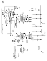
- FIG. 1 is a schematic diagram illustrating a configuration of a substrate processing apparatus according to an embodiment.
- FIG. 2 is a diagram showing in detail each of the coating unit 1 and the atmospheric transfer unit 2 shown in FIG.
- FIG. 3 shows the coating unit 1 shown in FIGS. 1 and 2 in detail.
- 4A is a plan view of the spin coater shown in FIG. 1
- FIG. 4B is a view of the spin coater shown in FIG. 5A is an SEM cross-sectional image of the 5 ⁇ m PZT thick film of the present invention (Example)
- FIG. 5B is an SEM cross-sectional image of the 5 ⁇ m PZT thick film of Conventional Example 1.
- FIG. 1 is a schematic diagram illustrating a configuration of a substrate processing apparatus according to an embodiment.
- FIG. 2 is a diagram showing in detail each of the coating unit 1 and the atmospheric transfer unit 2 shown in FIG.
- FIG. 3 shows the coating unit 1 shown in FIGS. 1 and 2 in detail.
- 4A is
- FIGS. 6A and 6B are diagrams comparing the D-E hysteresis characteristics of the PZT thick film of the present invention (Example) and the PZT thick film of Conventional Example 1.
- FIG. FIGS. 7A and 7B are diagrams comparing the leakage current densities of the PZT thick film of the present invention (Example) and the PZT thick film of Conventional Example 1.
- FIG. 8A to 8C are diagrams showing the results of Raman spectroscopic analysis of the PZT thick film of the present invention (Example) and the PZT thick film of Conventional Example 1.
- FIG. FIG. 9 is a schematic diagram showing the concept of pressurized RTA.
- FIG. 10 is a diagram showing the concentration distribution in the depth direction of the PZT thick film of the present invention (Example) sintered with pressurized oxygen.
- FIG. 11 is a diagram showing the concentration distribution in the depth direction of the PZT thick film of Conventional Example 2 sintered with atmospheric pressure oxygen.
- FIG. 1 is a schematic diagram showing the configuration of the substrate processing apparatus according to the present embodiment.
- FIG. 2 is a diagram showing in detail each of the coating unit 1 and the atmospheric transfer unit 2 in the substrate processing apparatus shown in FIG.
- FIG. 3 shows the coating unit 1 shown in FIGS. 1 and 2 in detail.
- 4A is a plan view of the spin coater shown in FIG. 1, and FIG.
- the substrate processing apparatus has a coating unit 1 having a spin coater 4 and an atmospheric transfer unit 2 having a transfer chamber 2a.
- the coating unit 1 will be described in detail.
- the atmospheric transfer unit 2 will be described later.
- the coating unit 1 has an exhaust mechanism 1a that exhausts the inside of the coating unit 1 and the inside of the spin coat processing chamber 4a.
- the spin coater 4 includes a spin coat processing chamber 4a for applying a film on the substrate 20 by spin coating, a holding mechanism 21 for holding the substrate disposed in the spin coat processing chamber 4a, and a motor for rotating the substrate 20.
- the rotating mechanism 22 having The coating unit 1 is provided with an air conditioning mechanism that adjusts the amount of dust in the air in the spin coat processing chamber 4a.
- This air conditioning mechanism has a hepa filter. With this air conditioning mechanism, the amount of dust in the air in the spin coat processing chamber 4a can be reduced compared to the outside air. Note that this air conditioning mechanism can also control the temperature, humidity, or air volume in the spin coat processing chamber 4a.
- the holding mechanism 21 has a stage, and holds the back surface of the substrate placed on the stage by evacuating the vacuum pump DP. Connected to the holding mechanism 21 is a mechanism for releasing the atmosphere after the back surface of the substrate is evacuated. As shown in FIGS.
- the spin coater 4 has a cup 61 that covers the periphery of the substrate 20 held by the holding mechanism 21.
- a movement mechanism 62 having a cylinder is connected to the cup 61, and this movement mechanism 62 is a mechanism for moving the cup 61 up and down.
- the cup 61 is connected to a waste liquid tank 63 through a pipe, and this waste liquid tank 63 is a tank into which a liquid stored in the cup 61 is put by performing a spin coating process.
- the waste liquid tank 63 is connected to the waste liquid tank 64 via the pump P.
- the spin coater 4 has a cleaning nozzle 67, and the cleaning nozzle 67 is connected to a cleaning liquid supply source 66 through a valve and a pipe.
- the cleaning nozzle 67 is attached to the first swing arm 70, and the first swing arm 70 is configured to rotate by a motor (see FIG. 4A). Thereby, when supplying the cleaning liquid to the substrate 21, the cleaning nozzle 67 can be moved above the substrate.
- a cup 75 for receiving the cleaning liquid is disposed at the standby position of the cleaning nozzle 67.
- the cup 75 is connected to the waste liquid tank 63 via a pipe.
- the spin coater 4 has a blow nozzle 68, and this blow nozzle 68 is connected to a nitrogen gas supply source for pressure feeding and substrate blowing through a valve and piping.
- the blow nozzle 68 is attached to the first swing arm. Thereby, when supplying nitrogen gas to the surface of the substrate 21, the blow nozzle 68 can be moved above the substrate.
- the piping connecting the cleaning liquid supply source 66 and the cleaning nozzle 67 is configured so that the cleaning liquid is pressure-fed by nitrogen gas by connecting a nitrogen gas supply source for pressure feeding and substrate blowing through a valve.
- the spin coater 4 has a dripping nozzle 72, and this dripping nozzle 72 is connected to a chemical material supply source 71 through a pipe and a dispensing system 65.
- the dripping nozzle 72 is attached to a second swing arm 73, and the second swing arm 73 is configured to rotate by a motor 74 (see FIG. 4). Thereby, when supplying a chemical material to the board
- the dispensing system 65 is a system in which a chemical material is sent from a chemical material supply source 71 to a dropping nozzle 72 and dropped onto a substrate.
- the dispensing system 65 is connected to the waste liquid tank 63 via a pipe. Further, a vacuum pump DP is connected to the dispensing system 65 via a pipe.
- the dispensing system 65 is connected to a nitrogen gas supply source for pressure feeding and substrate blowing through piping and valves.
- a cup 76 that receives a chemical material is disposed at a standby position of the dropping nozzle 72, and a liquid level sensor that detects the liquid level in the cup is provided in the cup 76.
- the cup 76 is connected to the waste liquid tank 63 via a valve and piping.
- the cup 76 is connected to a cleaning liquid supply source 66 through piping and valves. Thereby, the dripping nozzle 72 can be cleaned with the cleaning liquid.
- the spin coater 4 has an edge rinse nozzle 77, and the edge rinse nozzle 77 is connected to a cleaning liquid supply source via a valve and a pipe.
- the edge rinse nozzle 77 is attached to the third swing arm 78.
- the third swing arm 78 is configured to rotate by a motor 79, and is configured to move up and down by a cylinder 80 (see FIG. 4). Thus, the edge rinse nozzle 77 can be moved above the substrate when supplying the cleaning liquid to the edge of the surface of the substrate 21.
- a cup 81 for receiving the cleaning liquid is disposed at the standby position of the edge rinse nozzle 77, and this cup 81 is connected to the waste liquid tank 63 via a pipe.
- the cup 61 is connected to a cleaning liquid supply source 66 through a pipe and a valve. Thereby, the cup 61 can be cleaned with the cleaning liquid.
- the spin coater 4 has a back surface rinsing nozzle 82 for rinsing the back surface of the substrate, and the back surface rinsing nozzle 82 is disposed in the cup 61.
- the back surface rinsing nozzle 82 is connected to the cleaning liquid supply source 66 through a pipe and a valve. Thereby, the back surface of the substrate can be cleaned with the cleaning liquid.
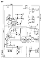
- the atmospheric transfer unit 2 includes a drying device 5 having a drying treatment chamber 5a for drying at a temperature of 150 ° C. to 300 ° C., a temperature of 300 to 600 ° C. in a nitrogen atmosphere or an inert gas atmosphere, Temporary nitrogen baking apparatus 6 having temporary nitrogen baking chamber 6a for temporary baking at normal pressure, pressurizing lamp annealing apparatus 7 having annealing chamber 7a, cooling apparatus 8 having cooling chamber, aligner 9 having alignment chamber A load / unload apparatus 10 having a load / unload chamber 10a and a transport mechanism 11 are disposed.
- the transfer chamber 2a of the atmospheric transfer unit 2 is connected to the spin coat processing chamber 4a via the gate valve 23, connected to the load / unload chamber 10a, connected to the alignment processing chamber, connected to the cooling processing chamber, and dried. It is connected to the processing chamber 5a, connected to the temporary baking processing chamber 6a via the gate valve 24, and connected to the annealing processing chamber 7a via the gate valve 25.
- the transport mechanism 11 of the atmospheric transport unit 2 includes a spin coat processing chamber 4a, a load / unload chamber 10a, an alignment processing chamber, a cooling processing chamber, a drying processing chamber 5a, a pre-baking processing chamber 6a, an annealing processing chamber 7a, and a loading chamber 12a.
- the atmospheric transfer unit 2 is provided with an air conditioning mechanism that adjusts the amount of dust in the air in the transfer chamber 2a.
- This air conditioning mechanism has a hepa filter (see FIG. 2). With this air conditioning mechanism, the amount of dust in the air in the transfer chamber 2a can be reduced compared to the outside air. In addition, this air-conditioning mechanism can also control the temperature or humidity in the transfer chamber 2a.
- the load / unload chamber 10 a of the load / unload apparatus 10 is for introducing or discharging a substrate into the atmospheric transfer unit 2.
- the alignment processing chamber of the aligner 9 is connected to the inside of the transfer chamber 2a and is a processing chamber for performing processing for detecting the center position of the surface of the substrate 20.
- the aligner 9 is provided with an air conditioning mechanism for adjusting the amount of dust in the air in the alignment processing chamber. Thereby, the amount of dust in the air in the alignment processing chamber can be reduced compared to the outside air. Note that this air conditioning mechanism can also control the temperature or humidity in the alignment processing chamber.
- the drying processing chamber 5 a of the drying device 5 is a processing chamber that performs a drying process on the film applied on the substrate by the spin coater 4. This drying process is a process for removing alcohol, moisture, and the like from the film, for example. As shown in FIG.
- a hot plate 42 for holding and heating the substrate 41 is disposed in the drying processing chamber 5a.
- a thermometer 43 is connected to the hot plate 42, and the hot plate 42 can be heated to a desired temperature (for example, 200 ° C.).
- the substrate 41 can be moved up and down by a lift 44 having pins.
- the drying device 5 has an exhaust mechanism 46 that exhausts the inside of the drying processing chamber 5a.
- the exhaust mechanism 46 has an exhaust port 45 disposed so as to face the substrate 41 held by the hot plate 42, and the air on the surface of the film coated on the substrate 41 is directly supplied from the exhaust port 45. Can be exhausted.
- the pre-baking treatment chamber 6a of the pre-baking apparatus 6 is a processing chamber for pre-baking a film applied on the substrate 41 at a desired temperature (for example, 300 ° C. to 600 ° C.) in a nitrogen atmosphere.
- a lamp heater 42 a for holding and heating the substrate 41 is disposed in the temporary baking apparatus 6.
- a thermometer 43 is connected to the lamp heater 42a, and the lamp heater 42a can be heated to a desired temperature.
- the substrate 41 can be moved up and down by a lift 44 having pins.
- the pre-baking apparatus 6 has a gas introduction mechanism for making the inside of the pre-baking treatment chamber 6a a predetermined atmosphere, and an exhaust system (such as a vacuum pump) for exhausting the inside of the pre-baking treatment chamber 6a.
- the gas introduction mechanism introduces nitrogen, for example.
- the pre-baking chamber 6a is connected to a nitrogen gas supply source, an oxygen gas supply source, or a dry air supply source via piping, valves, and a mass flow controller MFC1. Further, the inside of the pre-baking treatment chamber 6a can be depressurized to about 10 ⁇ 2 Pa by an exhaust system having a vacuum pump such as a dry pump.
- the annealing chamber 7a of the pressurizing lamp annealing apparatus 7 is a processing chamber for performing a lamp annealing process on the film applied on the substrate at a temperature of 500 to 1000 ° C., for example. This lamp annealing treatment can be performed in any state of pressurization, normal pressure, and reduced pressure.
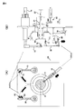
- the pressure-type lamp annealing apparatus 7 has an Al chamber 51, and the chamber 51 is configured to be water-cooled by a cooling mechanism (not shown).
- a mounting table 53 for mounting a substrate is provided in the chamber 51.
- the mounting table 53 is made of a material that transmits lamp light, for example, quartz.
- a quartz glass 54 is disposed above the mounting table 53.
- a lamp heater 55 is disposed on the quartz glass 54, and the lamp heater 55 is disposed inside a metal housing 56.
- An exhaust duct 57 is connected to the upper part of the housing 56, and the exhaust duct 57 exhausts heat in the housing 56.
- a window is provided in the lower part of the chamber 51 located below the mounting table 53, and calcium fluoride 58 is disposed in this window.
- a radiation thermometer 59 is disposed below the calcium fluoride 58.
- the calcium fluoride 58 is arranged to take in light in the wavelength region to be measured (infrared light having a wavelength of 5 ⁇ m).
- the present apparatus 7 has a thermometer 52 for measuring the temperature in the annealing chamber 7a.
- the annealing chamber 7a in the chamber 51 is connected to a pressurization line (pressurization mechanism) C2.
- the pressurization line C2 has a pressurization line using argon gas, a pressurization line using oxygen gas, and a pressurization line using nitrogen gas.
- the annealing chamber 7a in the chamber 1 is connected to a pressure adjustment line.
- the pressure adjusting line and the pressurizing line C2 can pressurize the annealing chamber 7a in the chamber 51 to a predetermined pressure (for example, less than 1 MPa).
- the pressure adjusting line includes a variable valve 69, and one side of the variable valve 69 is connected to the annealing chamber 7a via a pipe.
- the piping is connected to a pressure gauge DG, and the pressure inside the annealing chamber 7a can be measured by the pressure gauge DG.
- the other side of the variable valve 69 is connected to piping.
- the annealing chamber 7a is connected to a safety line.
- This safety line is for lowering the inside of the annealing chamber 7a to atmospheric pressure when the inside of the annealing chamber 7a is abnormally pressurized and becomes a certain pressure or higher.
- the safety line is equipped with an open valve.
- One side of the open valve is connected to the annealing chamber 7a via a pipe, and the other side of the open valve is connected to the pipe.
- the release valve allows gas to flow when a certain pressure is applied.
- the annealing chamber 7a is connected to an open air line. This air release line returns the inside of the annealing chamber 7a that has been normally pressurized to atmospheric pressure.
- the atmosphere open line is equipped with an open valve.
- One side of the open valve is connected to the annealing chamber 7a via a pipe, and the other side of the open valve is connected to the pipe.
- the opening valve is configured to gradually flow the gas in the annealing chamber 7a in order to return the annealing chamber 7a to atmospheric pressure.
- the annealing chamber 7a is connected to a line that returns the pressure from the reduced pressure state to the atmospheric pressure. This line returns the pressure from the reduced pressure state to the atmospheric pressure when the annealing chamber 7a is in a reduced pressure state (vacuum state).
- the line is equipped with a leak valve.
- One side of the leak valve is connected to the annealing chamber 7a via a pipe, and the other side of the leak valve is connected to a flow rate adjusting valve via the pipe.
- This flow rate adjusting valve is connected to a nitrogen gas supply source via a pipe. That is, the line returns the atmospheric pressure inside the annealing chamber 7a by gradually introducing nitrogen gas into the annealing chamber 7a from the nitrogen gas supply source through the flow rate adjusting valve and the leak valve. .
- the annealing chamber 7a is connected to a vacuum exhaust line for reducing the pressure inside the chamber 7a.
- the evacuation line has a valve, and one end of the valve is connected to the annealing chamber 7a through a pipe. The other end of the valve is connected to a vacuum pump via a pipe.
- This evacuation line is used, for example, when evacuating once before performing pressurized RTA.
- Each of the casing 56 and the lamp heater 55 is connected to a dry air supply source A2 through a pipe.
- the cooling processing chamber of the cooling device 8 is a processing chamber for cooling a substrate on which a drying process, a temporary baking process, a lamp annealing process, or the like has been performed.
- bulb mentioned above is connected to the compressed air supply source for valve drive via piping.
- Each of the alignment processing chamber of the aligner 9 and the transfer chamber 2a of the atmospheric transfer unit 2 is connected to the vacuum pump DP2 via a pipe.
- This thin film is a ferroelectric film such as a PZT film.
- the amount of dust in the air is adjusted in the transfer chamber 2a by the air conditioning mechanism, and the amount of dust in the air is adjusted in the alignment processing chamber by the air conditioning mechanism.
- processing for detecting the center position of the surface of the substrate is performed in the alignment processing chamber. This processing is performed in order to detect the center position of the substrate surface and to match the center position of the substrate surface with the rotation center of the substrate when performing the spin coating process.
- the gate valve 23 of the spin coat processing chamber 4a is opened, and the substrate in the alignment processing chamber is transferred into the spin coat processing chamber 4a through the transfer chamber 2a by the transfer mechanism 11, and this substrate is transferred to the spin coat processing chamber 4a.
- the gate valve 23 is closed by the holding mechanism 21 inside.
- the amount of dust in the air is adjusted in the spin coat processing chamber 4a by an air conditioning mechanism. Thereafter, a step of applying a film by spin coating on the substrate in the spin coat processing chamber 4a is performed.
- This process will be described in detail below.
- the substrate is rotated while supplying the cleaning liquid onto the substrate by the cleaning nozzle 67. Thereby, the surface of the substrate is cleaned.
- the supply of the cleaning liquid is stopped, and the cleaning liquid on the substrate is removed by rotating the substrate.
- the substrate is rotated while dropping the chemical material onto the substrate by the dropping nozzle 72.
- the cleaning liquid is dropped onto the edge of the substrate surface by the edge rinse nozzle 77. Thereby, a chemical material film is applied on the substrate.
- the cleaning liquid is dropped on the edge of the substrate surface is that when the film is applied onto the substrate by spin coating, the film thickness at the edge of the substrate is formed thicker than the center of the substrate. This is to apply while removing. Accordingly, it is preferable to move the edge of the cleaning liquid gradually from the end of the substrate toward the center by moving the edge rinse nozzle 77 gradually from the end of the substrate toward the center.
- the chemical material is supplied onto the substrate from one chemical material supply source 71.
- a plurality of chemical material supply sources are arranged and a plurality of materials are mixed in a predetermined manner. You may supply the chemical material mixed by ratio on a board
- the gate valve 23 of the spin coat processing chamber 4a is opened, and the substrate in the spin coat processing chamber 4a is transferred into the drying processing chamber 5a through the transfer chamber 2a by the transfer mechanism 11, and this substrate is transferred to the drying processing chamber. Holding by the holding mechanism in 5a, the gate valve 23 is closed. Then, the process which performs a drying process to the chemical material film
- the substrate is heated to, for example, 200 to 250 ° C.
- the gate valve 24 of the pre-baking chamber 6a is opened, the substrate in the drying chamber is transferred by the transfer mechanism 11 into the pre-baking chamber 6a through the transfer chamber 2a, and this substrate is transferred to the pre-baking chamber 6a.
- the gate valve 24 is closed by the holding mechanism inside. Thereafter, a process of pre-baking the chemical material film on the substrate in the pre-baking chamber 6a is performed.
- the inside of the pre-baking treatment chamber 6a is evacuated by an exhaust system, the inside of the pre-baking treatment chamber 6a is set to a normal pressure in a vacuum atmosphere, a nitrogen atmosphere or an inert gas atmosphere by a gas introduction mechanism, Temporary baking is performed by heating the chemical material film on the substrate to a desired temperature (for example, 300 ° C. to 600 ° C.). Thereafter, the gate valve 24 is opened, and the substrate in the temporary baking chamber 6a is transferred by the transfer mechanism 11 into the cooling processing chamber of the cooling device 8 through the transfer chamber 2a, and this substrate is transferred by the holding mechanism in the cooling chamber. Hold and close the gate valve 24. Thereafter, the substrate is cooled to a predetermined temperature in the cooling processing chamber.
- a desired temperature for example, 300 ° C. to 600 ° C.
- the substrate in the cooling processing chamber is transferred by the transfer mechanism 11 to the alignment processing chamber of the aligner 9 through the transfer chamber 2a, and this substrate is processed to detect the center position of the surface of the substrate in the alignment processing chamber.
- the gate valve 23 of the spin coat processing chamber 4a is opened, and the substrate in the alignment processing chamber is transferred into the spin coat processing chamber 4a through the transfer chamber 2a by the transfer mechanism 11, and this substrate is transferred to the spin coat processing chamber 4a.
- the gate valve 23 is closed by the holding mechanism 21 inside.
- a plurality of chemical material films are stacked on the substrate by repeating the spin coating process, the drying process, and the pre-baking process a plurality of times (for example, 30 times).
- a thicker film for example, a film thickness of 1 ⁇ m or more
- productivity can be improved by using the substrate processing apparatus described above.
- the spin coat process, the drying process, and the pre-baking process can be automatically performed by operating the substrate processing apparatus as described above by the control unit (not shown). For this reason, it is conceivable that each process is performed individually, and if the operator transports the substrate by hand, the hands may be numb, the processing order may be wrong, or the substrate may be dropped during transport, but this does not happen. There is an advantage. Therefore, productivity can be improved in mass production, and yield can be increased.
- the gate valve 24 of the pre-baking treatment chamber 6a is opened, the gate valve 25 of the pressure-type lamp annealing apparatus 7 is opened, and the substrate in the pre-baking treatment chamber 6a is annealed by the transfer mechanism 11 through the transfer chamber 2a.
- the substrate is transferred into the chamber 7a, the substrate is held by a holding mechanism, and the gate valves 24 and 25 are closed.
- the transfer time for transferring the substrate from the pre-baking chamber 6a to the annealing chamber 7a is 10 seconds or less. The reason for shortening the conveyance time in this way is as follows. If the transport time is long, the characteristics of the ferroelectric film are greatly affected.
- the chemical material film has a very high oxygen activity and is in an oxygen-deficient state, so that it is combined with oxygen in the atmosphere and the film characteristics deteriorate. Therefore, it is preferable to shorten the conveyance time.
- a lamp annealing process is performed on the plurality of layers of chemical material films on the substrate in the annealing chamber 7a.
- the annealing chamber 7a is set to a predetermined pressure (pressurization, normal pressure or reduced pressure) in a predetermined atmosphere, and the lamp material 55 is used to heat the chemical material film on the substrate to a desired temperature.
- the chemical material film is a ferroelectric film
- the ferroelectric film is crystallized by annealing.
- the substrate in the annealing chamber 7a is transferred by the transfer mechanism 11 into the load / unload chamber 10a through the transfer chamber 2a, and the substrate is unloaded.
- a thin film is produced on a substrate using the substrate processing apparatus shown in FIGS.
- the coating amount per one time was 500 uL, and the PZT thick film coating was performed on the substrate using the following spin conditions. Increase to 0-300 rpm in 3 seconds, hold for 3 seconds, then increase to 300-500 rpm for 5 seconds, hold for 5 seconds, then increase to 500-1500 rpm for 5 seconds Raise and hold for 90 seconds.
- the substrate was held for 30 seconds on a hot plate heated to 250 ° C., and moisture was removed from the applied PZT thick film.
- the temporary baking process was performed to the sample given to said drying process. Specifically, evacuation of the pre-baking chamber 6a was performed with a rotary pump, and the ultimate vacuum was set to 10 ⁇ 1 Pa.
- the inside of the pre-baking chamber 6a was filled with N 2 to atmospheric pressure, and the substrate was heated at 450 ° C. for 90 seconds to decompose and remove organic components.
- a pre-baking step different from that of the present example was performed on the sample subjected to the above drying step.
- pre-baking was performed at 450 ° C. for 90 seconds in atmospheric air (containing oxygen).
- This sample is referred to as Conventional Example 1.
- the above-described spin coating, drying step, and pre-baking step were repeated 15 times to produce samples (Example and Conventional Example 1) in which a PZT thick film having a total film thickness of 5 ⁇ m was formed on the substrate.
- the PZT thick film was crystallized by performing a lamp annealing treatment on the 5 ⁇ m thick PZT film on each substrate of the above samples (Example and Conventional Example 1) using a rapid heating apparatus (RTA).
- RTA rapid heating apparatus
- the PZT thick film of this example is heated to a temperature of 700 ° C.
- FIG. 5B is an SEM cross-sectional image of the conventional 5 ⁇ m PZT thick film.
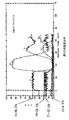
- FIG. 6A is a diagram showing the results of the hysteresis evaluation of the 5 ⁇ m PZT thick film of the present invention (Example), and FIG. 6B is the hysteresis evaluation of the 5 ⁇ m PZT thick film of Conventional Example 1. It is a figure which shows a result. As shown in FIG. 6A, in the present invention (Example), good hysteresis was obtained, whereas in Conventional Example 1, as shown in FIG. 6B, a very distorted small hysteresis curve and became.
- FIG. 6A is a diagram showing the results of the hysteresis evaluation of the 5 ⁇ m PZT thick film of the present invention (Example)
- FIG. 6B is the hysteresis evaluation of the 5 ⁇ m PZT thick film of Conventional Example 1. It is a figure which shows
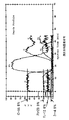
- FIG. 7A is a diagram showing the result of measuring the leakage current density for the 5 ⁇ m PZT thick film of the present invention (Example), and FIG. 7B is the leakage current for the 5 ⁇ m PZT thick film of Conventional Example 1. It is a figure which shows the result of having measured the density. As shown in FIG. 7 (A), the present invention showed good leak characteristics, whereas as shown in FIG. 7 (B), Conventional Example 1 has 10 ⁇ 6 to 10 ⁇ 3 A / cm 2 . A very large leakage current was observed.
- FIG. 8A is a diagram showing the results of Raman spectroscopic analysis of the 5 ⁇ m PZT thick film of the present invention (Example), and FIG.
- FIG. 8B is the result of Raman spectroscopic analysis of the 5 ⁇ m PZT thick film of Conventional Example 1.
- FIG. 8C is an enlarged view of B shown in FIG. 8B.
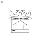
- the pressurized RTA was further examined in detail. The concept of the pressurized RTA is as shown in FIG. Specifically, PZT crystal initial nuclei are generated by excess lead, but since the PZT crystal itself is stoichiometry, excess lead accumulated in the upper part of the thin film with pressurized oxygen is removed by accelerating oxidation with pressurized oxygen. .
- Pb Zr + Ti
- FIG. 10 and FIG. 11 show that Conventional Example 2 contains more oxygen.
- Conventional Example 2 contains more oxygen than the PZT thick film of the present invention. This is thought to be because the Pb component, which is often observed in Conventional Example 2, is present at the PZT grain boundary as an impurity called PbOx.
Abstract
基板上に塗布された膜に塵が付着するのを抑制できる基板処理装置を提供する。本発明の一態様は、基板上に膜をスピンコートにより塗布するためのスピンコート処理室4aと、前記スピンコート処理室内の空気中の塵の量を調整する第1の空調機構と、前記基板上に塗布された膜にランプアニール処理を行うためのアニール処理室7aと、前記スピンコート処理室および前記アニール処理室それぞれに繋げられ、前記スピンコート処理室と前記アニール処理室の相互間において前記基板を搬送するための搬送室2aと、前記搬送室内の空気中の塵の量を調整する第2の空調機構と、を具備することを特徴とする基板処理装置である。
Description
本発明は、スピンコータを備えた基板処理装置及びその基板処理装置を用いて薄膜を製造する方法に関する。
従来のPZT膜の製造方法について説明する。
4インチウエハ上に例えば(111)に配向したPt膜を形成し、このPt膜上にスピンコータによってPZTゾルゲル溶液を回転塗布する。次に、この塗布されたPZTゾルゲル溶液をホットプレート上で加熱保持して乾燥させ、水分を除去した後、さらに高温に保持したホットプレート上で加熱保持して仮焼成を行う。これを複数回繰り返しPZTアモルファスを生成する。
次いで、仮焼成を行った後のPZTアモルファスに加圧式ランプアニール装置(RTA:rapidly thermal anneal)を用いてアニール処理を行ってPZT結晶化を行う(例えば特許文献1参照)。
4インチウエハ上に例えば(111)に配向したPt膜を形成し、このPt膜上にスピンコータによってPZTゾルゲル溶液を回転塗布する。次に、この塗布されたPZTゾルゲル溶液をホットプレート上で加熱保持して乾燥させ、水分を除去した後、さらに高温に保持したホットプレート上で加熱保持して仮焼成を行う。これを複数回繰り返しPZTアモルファスを生成する。
次いで、仮焼成を行った後のPZTアモルファスに加圧式ランプアニール装置(RTA:rapidly thermal anneal)を用いてアニール処理を行ってPZT結晶化を行う(例えば特許文献1参照)。
従来の製造方法では、スピンコータによって基板上に溶液を回転塗布する工程、ウエハをスピンコータとアニール装置との間を搬送する工程によって塵、ゴミ、コンタミ等が基板上に塗布された膜に付着するという課題がある。
また、基板上に非常に厚い膜を形成することが求められる場合があり、この場合は、スピンコータによって基板上に溶液を回転塗布する工程と、この塗布された膜を仮焼成する工程とを多数回繰り返す必要がある。このような場合、スピンコータと仮焼成装置との間の基板搬送をオペレータが行うのでは生産性を高めるのに限界がある。
本発明の一態様は、基板上に塗布された膜に塵が付着するのを抑制できる基板処理装置及びその基板処理装置を用いた薄膜の製造方法を提供することを課題とする。
また、本発明の一態様は、基板上に非常に厚い膜を形成する場合に生産性を向上できる基板処理装置及びそれを用いた薄膜の製造方法を提供することを課題とする。
本発明の一態様は、基板上に膜をスピンコートにより塗布するためのスピンコート処理室と、
前記スピンコート処理室内の空気中の塵の量を調整する第1の空調機構と、
前記基板上に塗布された膜にランプアニール処理を行うためのアニール処理室と、
前記スピンコート処理室および前記アニール処理室それぞれに繋げられ、前記スピンコート処理室と前記アニール処理室の相互間において前記基板を搬送するための搬送室と、
前記搬送室内の空気中の塵の量を調整する第2の空調機構と、
を具備することを特徴とする基板処理装置である。
また、本発明の一態様において、
前記搬送室内に繋げられ、前記基板上に塗布された膜に仮焼成を行うための仮焼成処理室をさらに具備することも可能である。
また、本発明の一態様において、
前記搬送室に繋げられ、前記基板上に塗布された膜に乾燥処理を行うための乾燥処理室と、
前記乾燥処理室内を排気する排気機構と、
をさらに具備することも可能である。
また、本発明の一態様において、
前記乾燥処理室内には前記基板を保持する保持機構が配置され、
前記排気機構は、前記保持機構に保持される前記基板と対向させて配置された排気口を有し、前記基板に塗布された膜の表面上の空気を前記排気口から直接的に排気することも可能である。
また、本発明の一態様において、
前記搬送室内に繋げられ、前記基板の表面の中心位置の検出を行うためのアライメント処理室と、
前記アライメント処理室内の空気中の塵の量を調整する第3の空調機構と、
をさらに具備することも可能である。
また、本発明の一態様において、
前記搬送室内には前記基板を搬送する搬送機構が設けられていることも可能である。
また、本発明の一態様において、
前記第1の空調機構は、温度または湿度または風量を制御することも可能である。
また、本発明の一態様において、
前記ランプアニール処理は加圧、常圧および減圧のいずれかの状態で行われることも可能である。
本発明の一態様は、上述した基板処理装置を用いて基板上に薄膜を製造する方法であって、
前記第1の空調機構によって空気中の塵の量が調整された前記スピンコート処理室内で前記基板上にスピンコートにより膜を塗布する第1工程と、
前記第1工程の後に、前記スピンコート処理室内の前記基板を、前記搬送室を通って前記仮焼成処理室内に搬送する第2工程と、
前記第2工程の後に、前記仮焼成処理室内で前記基板上の前記膜に仮焼成を行う第3工程と、
前記第3工程の後に、前記仮焼成処理室内の前記基板を、前記搬送室を通って前記スピンコート処理室内に搬送する第4工程、前記第1工程、前記第2工程、前記第3工程を繰り返すことにより、前記基板上に複数の膜を積層して形成する第5工程と、
前記第5工程の後に、前記仮焼成処理室内の前記基板を、前記搬送室を通って前記アニール処理室内に搬送する第6工程と、
前記第6工程の後に、前記アニール処理室内で前記基板上の前記複数の膜にランプアニール処理を行う第7工程と、
を具備し、
前記搬送室は、前記第2の空調機構によって空気中の塵の量が調整されていることを特徴とする薄膜の製造方法である。
また、本発明の一態様において、
前記仮焼成は、真空雰囲気中または窒素雰囲気中または不活性ガス雰囲気中で行われることが好ましい。
本発明の一態様によれば、基板上に塗布された膜に塵が付着するのを抑制できる基板処理装置及びそれを用いた薄膜の製造方法を提供することができる。
また、本発明の一態様によれば、基板上に非常に厚い膜を形成する場合に生産性を向上できる基板処理装置及びそれを用いた薄膜の製造方法を提供することができる。
また、本発明の一態様によれば、基板上に非常に厚い膜を形成する場合に生産性を向上できる基板処理装置及びそれを用いた薄膜の製造方法を提供することができる。
図1は、実施形態による基板処理装置の構成を示す模式図である。
図2は、図1に示すコーティングユニット1および大気搬送ユニット2それぞれを詳細に示す図である。
図3は、図1及び図2に示すコーティングユニット1を詳細に示す図である。
図4(A)は図1に示すスピンコータの平面図であり、図4(B)は図4(A)に示すスピンコータのA矢視図である。
図5(A)は本発明(実施例)の5μmPZT厚膜のSEM断面像であり、図5(B)は従来例1の5μmPZT厚膜のSEM断面像である。
図6(A),(B)は本発明(実施例)のPZT厚膜と従来例1のPZT厚膜とのD−Eヒステリシス特性を比較した図である。
図7(A),(B)は本発明(実施例)のPZT厚膜と従来例1のPZT厚膜についてのリーク電流密度を比較した図である。
図8(A)~(C)は本発明(実施例)のPZT厚膜と従来例1のPZT厚膜についてのラマン分光分析結果を示す図である。
図9は、加圧RTAのコンセプトを示す模式図である。
図10は、加圧酸素で焼結した本発明(実施例)のPZT厚膜の深さ方向の濃度分布を示す図である。
図11は、大気圧酸素で焼結した従来例2のPZT厚膜の深さ方向の濃度分布を示す図である。
以下では、本発明の実施形態について図面を用いて詳細に説明する。ただし、本発明は以下の説明に限定されず、本発明の趣旨及びその範囲から逸脱することなくその形態及び詳細を様々に変更し得ることは、当業者であれば容易に理解される。従って、本発明は以下に示す実施形態の記載内容に限定して解釈されるものではない。
図1は、本実施形態による基板処理装置の構成を示す模式図である。図2は、図1に示す基板処理装置におけるコーティングユニット1および大気搬送ユニット2それぞれを詳細に示す図である。図3は、図1及び図2に示すコーティングユニット1を詳細に示す図である。図4(A)は、図1に示すスピンコータの平面図であり、図4(B)は、図4(A)に示すスピンコータのA矢視図である。
図1に示すように、基板処理装置は、スピンコータ4を有するコーティングユニット1と、搬送室2aを有する大気搬送ユニット2を有している。
まず、コーティングユニット1について詳細に説明する。なお、大気搬送ユニット2については後述する。
図2に示すように、コーティングユニット1は、その内部及びスピンコート処理室4a内を排気する排気機構1aを有している。スピンコータ4は、基板20上に膜をスピンコートにより塗布するためのスピンコート処理室4aと、このスピンコート処理室4a内に配置された基板を保持する保持機構21と、基板20を回転させるモータを有する回転機構22を有している。
コーティングユニット1には、スピンコート処理室4a内の空気中の塵の量を調整する空調機構が設けられている。この空調機構は、ヘパフィルターを有している。この空調機構によってスピンコート処理室4a内の空気中の塵の量を外気に比べて少なくすることができる。なお、この空調機構は、スピンコート処理室4a内の温度または湿度または風量を制御することも可能である。
図3に示すように、保持機構21は、ステージを有しており、このステージ上に載置した基板の裏面を真空ポンプDPによって真空引きすることで保持するようになっている。保持機構21には、基板の裏面を真空引きした後に大気開放する機構が接続されている。
図3及び図4に示すように、スピンコータ4は、保持機構21によって保持された基板20の周囲を覆うカップ61を有している。カップ61にはシリンダーを有する移動機構62が接続されており、この移動機構62はカップ61を上下に移動させる機構である。
カップ61は配管を通して廃液タンク63に接続されており、この廃液タンク63はスピンコート処理が行われることによってカップ61に貯まる液体が入れられるタンクである。廃液タンク63はポンプPを介して廃液タンク64に接続されている。
また、スピンコータ4は洗浄ノズル67を有しており、その洗浄ノズル67はバルブ及び配管を介して洗浄液供給源66に接続されている。洗浄ノズル67は第1のスイングアーム70に取り付けられており、第1のスイングアーム70はモータによって回転移動するように構成されている(図4(A)参照)。これにより、基板21に洗浄液を供給する際に洗浄ノズル67を基板の上方に移動することができる。
洗浄ノズル67の待機位置には洗浄液を受けるカップ75が配置されている。このカップ75は、配管を介して廃液タンク63に接続されている。
また、スピンコータ4はブローノズル68を有しており、このブローノズル68はバルブ及び配管を介して圧送・基板ブロー用の窒素ガス供給源に接続されている。ブローノズル68は第1のスイングアームに取り付けられている。これにより、基板21の表面に窒素ガスを供給する際にブローノズル68を基板の上方に移動することができる。
洗浄液供給源66と洗浄ノズル67とを接続する配管は、バルブを介して圧送・基板ブロー用の窒素ガス供給源が接続されていることで、洗浄液が窒素ガスによって圧送されるように構成されている。
また、スピンコータ4は滴下ノズル72を有しており、この滴下ノズル72は配管及びディスペンスシステム65を介してケミカル材料供給源71に接続されている。滴下ノズル72は第2のスイングアーム73に取り付けられており、第2のスイングアーム73はモータ74によって回転移動するように構成されている(図4参照)。これにより、基板21にケミカル材料を供給する際に滴下ノズル72を基板の上方に移動することができる。
ディスペンスシステム65はケミカル材料供給源71からケミカル材料を滴下ノズル72へ送って基板上へ滴下させるシステムである。なお、ディスペンスシステム65は廃液タンク63に配管を介して接続されている。また、ディスペンスシステム65には配管を介して真空ポンプDPが接続されている。ディスペンスシステム65には配管及びバルブを介して圧送・基板ブロー用の窒素ガス供給源に接続されている。
滴下ノズル72の待機位置にはケミカル材料を受けるカップ76が配置されており、このカップ76にはカップ内の液面を感知する液面センサーが設けられている。このカップ76は、バルブ及び配管を介して廃液タンク63に接続されている。
また、カップ76には配管及びバルブを介して洗浄液供給源66に接続されている。これにより、滴下ノズル72を洗浄液によって洗浄することができるようになっている。
また、スピンコータ4はエッヂリンスノズル77を有しており、このエッヂリンスノズル77はバルブ及び配管を介して洗浄液供給源に接続されている。エッヂリンスノズル77は第3のスイングアーム78に取り付けられている。第3のスイングアーム78は、モータ79によって回転移動するように構成され、シリンダー80によって上下に移動するように構成されている(図4参照)。これにより、基板21の表面の端部に洗浄液を供給する際にエッヂリンスノズル77を基板の上方に移動することができる。
エッヂリンスノズル77の待機位置には洗浄液を受けるカップ81が配置されており、このカップ81は配管を介して廃液タンク63に接続されている。
また、カップ61は配管及びバルブを介して洗浄液供給源66に接続されている。これにより、カップ61を洗浄液によって洗浄することができるようになっている。
また、スピンコータ4は基板の裏面をリンスする裏面リンスノズル82を有しており、裏面リンスノズル82はカップ61内に配置されている。裏面リンスノズル82は配管及びバルブを介して洗浄液供給源66に接続されている。これにより、基板の裏面を洗浄液によって洗浄することができるようになっている。
また、上述したバルブは、配管を介してバルブ駆動用のエアー供給源に接続されている。
次に、大気搬送ユニット2について詳細に説明する。
図1に示すように、大気搬送ユニット2には、150℃~300℃の温度で乾燥させる乾燥処理室5aを有する乾燥装置5、窒素雰囲気または不活性ガス雰囲気で例えば300~600℃の温度、常圧で仮焼成を行う仮窒素焼成処理室6aを有する仮窒素焼成装置6、アニール処理室7aを有する加圧式ランプアニール装置7、冷却処理室を有する冷却装置8、アライメント処理室を有するアライナー9、ロード・アンロード室10aを有するロード・アンロード装置10および搬送機構11が配置されている。
大気搬送ユニット2の搬送室2aは、スピンコート処理室4aにゲートバルブ23を介して繋げられ、ロード・アンロード室10aに繋げられ、アライメント処理室に繋げられ、冷却処理室に繋げられ、乾燥処理室5aに繋げられ、ゲートバルブ24を介して仮焼成処理室6aに繋げられ、ゲートバルブ25を介してアニール処理室7aに繋げられている。
大気搬送ユニット2の搬送機構11は、スピンコート処理室4a、ロード・アンロード室10a、アライメント処理室、冷却処理室、乾燥処理室5a、仮焼成処理室6a、アニール処理室7a、ロード室12aおよびアンロード室13aそれぞれに基板20を搬送するための機構である。
大気搬送ユニット2には、搬送室2a内の空気中の塵の量を調整する空調機構が設けられている。この空調機構は、ヘパフィルターを有している(図2参照)。この空調機構によって搬送室2a内の空気中の塵の量を外気に比べて少なくすることができる。なお、この空調機構は、搬送室2a内の温度または湿度を制御することも可能である。
ロード・アンロード装置10のロード・アンロード室10aは、大気搬送ユニット2内に基板を導入または排出するためのものである。
アライナー9のアライメント処理室は、前記搬送室2a内に繋げられており、基板20の表面の中心位置を検出する処理を行うための処理室である。また、アライナー9にはアライメント処理室内の空気中の塵の量を調整する空調機構が設けられている。これにより、アライメント処理室内の空気中の塵の量を外気に比べて少なくすることができる。なお、この空調機構は、アライメント処理室内の温度または湿度を制御することも可能である。
乾燥装置5の乾燥処理室5aは、スピンコータ4によって基板上に塗布された膜に乾燥処理を行う処理室である。この乾燥処理は、例えば膜中のアルコール、水分などを除去する処理である。
図2に示すように、乾燥処理室5a内には、基板41を保持して加熱するためのホットプレート42が配置されている。このホットプレート42には温度計43が接続されており、ホットプレート42を所望の温度(例えば200℃)に加熱することができる。基板41は、ピンを有するリフト44によって上下に移動可能とされている。
乾燥装置5は、乾燥処理室5a内を排気する排気機構46を有している。この排気機構46は、ホットプレート42に保持される基板41と対向させて配置された排気口45を有しており、基板41上に塗布された膜の表面上の空気を排気口45から直接的に排気できるようになっている。
仮焼成装置6の仮焼成処理室6aは、基板41上に塗布された膜に窒素雰囲気中で所望の温度(例えば300℃~600℃)の仮焼成を行うための処理室である。仮焼成装置6内には、基板41を保持して加熱するためのランプヒータ42aが配置されている。このランプヒータ42aには温度計43が接続されており、ランプヒータ42aを所望の温度に加熱することができる。基板41は、ピンを有するリフト44によって上下に移動可能とされている。また、仮焼成装置6は、仮焼成処理室6a内を所定の雰囲気にするためのガス導入機構と、仮焼成処理室6a内を排気する排気系(真空ポンプ等)を有している。ガス導入機構は、例えば窒素を導入するものである。仮焼成処理室6aは、配管、バルブ及びマスフローコントローラーMFC1を介して窒素ガス供給源、酸素ガス供給源またはドライエアー供給源に接続されている。また、仮焼成処理室6a内は、ドライポンプ等の真空ポンプを有する排気系によって10−2Pa程度まで減圧可能とされている。
加圧式ランプアニール装置7のアニール処理室7aは、基板上に塗布された膜に例えば500~1000℃の温度でランプアニール処理を行うための処理室である。このランプアニール処理は加圧、常圧および減圧のいずれの状態でも行うことが可能である。
加圧式ランプアニール装置7について詳細に説明する。
図2に示すように、加圧式ランプアニール装置7はAl製のチャンバー51を有しており、チャンバー51は図示せぬ冷却機構によって水冷されるように構成されている。チャンバー51内には基板を載置する載置台53が設けられている。載置台53はランプ光が透過する材料、例えば石英で形成されている。載置台53の上方には石英ガラス54が配置されている。
また、石英ガラス54の上にはランプヒータ55が配置されており、このランプヒータ55は金属製の筐体56の内部に配置されている。筐体56の上部には排気ダクト57が接続されており、この排気ダクト57は筐体56内の熱を排気するものである。
また、載置台53の下方に位置するチャンバー51の下部には窓が設けられており、この窓にはフッ化カルシウム58が配置されている。フッ化カルシウム58の下方には放射温度計59が配置されている。フッ化カルシウム58は、放射温度計59で基板の温度を測定するために、測定する波長領域の光(波長5μmの赤外線)を取り込むために配置している。また、本装置7はアニール処理室7a内の温度を測定するための温度計52を有している。
また、チャンバー51内のアニール処理室7aは加圧ライン(加圧機構)C2に接続されている。加圧ラインC2は、アルゴンガスによる加圧ライン、酸素ガスによる加圧ライン及び窒素ガスによる加圧ラインを有している。
また、チャンバー1内のアニール処理室7aは圧力調整ラインに接続されている。この圧力調整ライン及び加圧ラインC2によってチャンバー51内のアニール処理室7aを所定の圧力(例えば1MPa未満)に加圧できるようになっている。前記圧力調整ラインは可変バルブ69を備えており、この可変バルブ69の一方側は配管を介してアニール処理室7aに接続されている。前記配管は圧力計DGに接続されており、この圧力計DGによってアニール処理室7a内の圧力を測定できるようになっている。可変バルブ69の他方側は配管に接続されている。
また、アニール処理室7aは安全ラインに接続されている。この安全ラインは、アニール処理室7a内が異常に加圧され過ぎてある一定の圧力以上になった時にアニール処理室7a内を大気圧まで下げるためのものである。安全ラインは開放バルブを備えている。この開放バルブの一方側は配管を介してアニール処理室7aに接続されており、開放バルブの他方側は配管に接続されている。開放バルブはある一定の圧力がかかるとガスが流れるようになっている。
また、アニール処理室7aは大気開放ラインに接続されている。この大気開放ラインは、正常に加圧されたアニール処理室7a内を大気圧に戻すものである。大気開放ラインは開放バルブを備えている。この開放バルブの一方側は配管を介してアニール処理室7aに接続されており、開放バルブの他方側は配管に接続されている。開放バルブは、アニール処理室7a内を大気圧に戻すためにアニール処理室7a内のガスを徐々に流すようになっている。
また、アニール処理室7aは減圧状態から大気圧に戻すラインに接続されている。このラインは、アニール処理室7a内が減圧状態(真空状態)となっている場合に、減圧状態から大気圧に戻すものである。前記ラインはリークバルブを備えている。このリークバルブの一方側は配管を介してアニール処理室7aに接続されており、リークバルブの他方側は配管を介して流量調整弁に接続されている。この流量調製弁は配管を介して窒素ガス供給源に接続されている。つまり、前記ラインは、窒素ガス供給源から流量調整弁、リークバルブを介してアニール処理室7a内に窒素ガスを徐々に導入することによりアニール処理室7a内を大気圧に戻すようになっている。
また、アニール処理室7aは、その処理室7a内を減圧状態にするための真空排気ラインに接続されている。この真空排気ラインはバルブを有しており、このバルブの一端は配管を介してアニール処理室7a内に接続されている。バルブの他端は配管を介して真空ポンプに接続されている。この真空排気ラインは、例えば加圧RTAを行う前に一度真空排気を行う場合などに使用される。
また、筐体56及びランプヒータ55それぞれは配管を介してドライエアー供給源A2に接続されている。ドライエアー供給源A2からドライエアーを筐体内及びランプヒータ内に導入することにより、筐体内及びランプヒータ内に溜まる熱を排気ダクト57から排気することができる。
冷却装置8の冷却処理室は、乾燥処理または仮焼成処理またはランプアニール処理などが行われた基板を冷却するための処理室である。
また、上述したバルブは、配管を介してバルブ駆動用の圧空供給源に接続されている。また、アライナー9のアライメント処理室及び大気搬送ユニット2の搬送室2aそれぞれは、配管を介して真空ポンプDP2に接続されている。
次に、上記の基板処理装置を用いて基板を処理することで基板上に薄膜を製造する方法について説明する。この薄膜は、例えばPZT膜などの強誘電体膜である。
まず、ロード・アンロード室10aに基板をロードする。
この後、搬送機構11によってロード・アンロード室10a内の基板を、搬送室2aを通ってアライナー9のアライメント処理室内に搬送し、この基板をアライメント処理室内の保持機構によって保持する。この際、搬送室2a内は、空調機構によって空気中の塵の量が調整されており、アライメント処理室内は、空調機構によって空気中の塵の量が調整されている。
この後、アライメント処理室内で基板の表面の中心位置を検出する処理を行う。この処理を行うのは、基板表面の中心位置を検出しておき、スピンコート処理を行う際に基板表面の中心位置と基板の回転中心を一致させるためである。
この後、スピンコート処理室4aのゲートバルブ23を開け、搬送機構11によってアライメント処理室内の基板を、搬送室2aを通ってスピンコート処理室4a内に搬送し、この基板をスピンコート処理室4a内の保持機構21によって保持し、ゲートバルブ23を閉じる。この際、スピンコート処理室4a内は、空調機構によって空気中の塵の量が調整されている。
この後、スピンコート処理室4a内で基板上にスピンコートにより膜を塗布する工程を行う。
この工程を以下に詳細に説明する。
洗浄ノズル67によって基板上に洗浄液を供給しつつ基板を回転させる。これにより、基板の表面が洗浄される。次に、洗浄液の供給を停止し、基板を回転させることで、基板上の洗浄液を除去する。
次に、滴下ノズル72によって基板上にケミカル材料を滴下しつつ基板を回転させる。これとともに、エッヂリンスノズル77によって基板表面の端部に洗浄液を滴下する。これにより、基板上にはケミカル材料膜が塗布される。基板表面の端部に洗浄液を滴下する理由は、基板上にスピンコートにより膜を塗布すると基板の端部の膜厚が基板の中央より厚く形成されるので、基板の端部の膜を洗浄液で除去しながら塗布するためである。従って、エッヂリンスノズル77を基板の端部から中央側に少しずつ移動させることで、洗浄液を滴下する位置を基板の端部から中央側に少しずつ移動させることが好ましい。
なお、本実施形態では、図3に示すように、一つのケミカル材料供給源71からケミカル材料を基板上に供給しているが、ケミカル材料供給源を複数配置し、複数の材料を所定の混合比で混合したケミカル材料を基板上に供給しても良い。この場合は、所望の混合比を制御できる制御機構を設けておけば、基板上に複数種類のケミカル材料を容易に且つオペレータが間違えることなく供給することができる。
この後、スピンコート処理室4aのゲートバルブ23を開け、搬送機構11によってスピンコート処理室4a内の基板を、搬送室2aを通って乾燥処理室5a内に搬送し、この基板を乾燥処理室5a内の保持機構によって保持し、ゲートバルブ23を閉じる。
この後、乾燥処理室5a内で基板上のケミカル材料膜に乾燥処理を施す工程を行う。
この工程を以下に詳細に説明する。
排気機構46によって基板上に塗布された膜の表面上の空気を排気口45から直接的に排気しながら、ホットプレート42によって基板を例えば200~250℃に加熱する。これにより、ケミカル材料膜中の水分等を除去する。排気口45は、ホットプレート42に保持された基板と対向させて配置されているため、基板上に塗布された膜の表面上の空気を効率よく排気することができる。
この後、仮焼成処理室6aのゲートバルブ24を開け、搬送機構11によって乾燥処理室内の基板を、搬送室2aを通って仮焼成処理室6a内に搬送し、この基板を仮焼成処理室6a内の保持機構によって保持し、ゲートバルブ24を閉じる。
この後、仮焼成処理室6a内で基板上のケミカル材料膜に仮焼成を施す工程を行う。
詳細には、排気系によって仮焼成処理室6a内を真空排気した後に、ガス導入機構によって仮焼成処理室6a内を真空雰囲気中または窒素雰囲気または不活性ガス雰囲気で常圧とし、ランプヒータ42aによって基板上のケミカル材料膜を所望の温度(例えば300℃~600℃)に加熱することで仮焼成を行う。
この後、ゲートバルブ24を開け、搬送機構11によって仮焼成処理室6a内の基板を、搬送室2aを通って冷却装置8の冷却処理室内に搬送し、この基板を冷却処理室内の保持機構によって保持し、ゲートバルブ24を閉じる。この後、冷却処理室内で基板を所定の温度まで冷却する。
この後、搬送機構11によって冷却処理室内の基板を、搬送室2aを通ってアライナー9のアライメント処理室内に搬送し、この基板をアライメント処理室内で基板の表面の中心位置を検出する処理を行う。
この後、スピンコート処理室4aのゲートバルブ23を開け、搬送機構11によってアライメント処理室内の基板を、搬送室2aを通ってスピンコート処理室4a内に搬送し、この基板をスピンコート処理室4a内の保持機構21によって保持し、ゲートバルブ23を閉じる。
この後、上述した方法と同様にスピンコート処理、乾燥処理、仮焼成処理の工程を複数回(例えば30回)繰り返すことにより、基板上に複数のケミカル材料膜を積層して形成する。このように繰り返す回数が多いほど基板上に厚い膜(例えば膜厚が1μm以上)を形成することができる。この場合に前述した基板処理装置を用いることにより生産性を向上させることができる。詳細には、基板処理装置を制御部(図示せす)によって上述したように動作せることにより、スピンコート処理、乾燥処理、仮焼成処理を自動で行うことができる。このため、それぞれの処理を個別に行い、オペレータが手で基板を搬送すると手がしびれたり処理の順序を間違えたり搬送中に基板を落としたりすることも考えられるが、このようなことが起こらないという利点がある。従って、大量生産する際に生産性を向上させることができ、歩留りを高めることができる。
この後、仮焼成処理室6aのゲートバルブ24を開け、加圧式ランプアニール装置7のゲートバルブ25を開け、搬送機構11によって仮焼成処理室6a内の基板を、搬送室2aを通ってアニール処理室7a内に搬送し、この基板を保持機構によって保持し、ゲートバルブ24,25を閉じる。なお、基板上のケミカル材料膜が強誘電体膜である場合は、仮焼成処理室6a内からアニール処理室7a内に基板を搬送する搬送時間が10秒以下であることが好ましい。
このように搬送時間を短くする理由は次のとおりである。搬送時間が長くなると強誘電体膜の特性に大きく影響を与える。詳細には、仮焼成後は、ケミカル材料膜の酸素活性が非常に高く酸素欠乏状態であるため、大気中の酸素と結合してしまい、膜の特性が劣化する。従って、搬送時間を短くすることが好ましい。
この後、アニール処理室7a内で基板上の複数層のケミカル材料膜にランプアニール処理を施す工程を行う。
詳細には、アニール処理室7a内を所定の雰囲気で所定の圧力(加圧、常圧または減圧)とし、ランプヒータ55によって基板上のケミカル材料膜を所望の温度に加熱することでアニール処理を行う。ケミカル材料膜が強誘電体膜である場合は、アニール処理によって強誘電体膜が結晶化される。
この後、搬送機構11によってアニール処理室7a内の基板を、搬送室2aを通ってロード・アンロード室10a内に搬送し、この基板をアンロードする。
本実施例は、図1~図4に示す基板処理装置を用いて基板上に薄膜を製造するものである。
25重量%Pb15%過剰ゾルゲルPZT溶液(Pb/Zr/Ti=115/52/48)を用いて基板上にスピンコートを行った。一回当たり塗布量は500uLとし、スピン条件は以下の条件を用いて基板上にPZT厚膜塗布を行った。
0~300rpmの回転速度に3秒で上昇させ、3秒間保持し、その後、300~500rpmの回転速度に5秒で上昇させ、5秒間保持し、その後、500~1500rpmの回転速度に5秒で上昇させ、90秒間保持する。
次に、乾燥工程として250℃に加熱したホットプレート上で基板を30秒保持し、塗布したPZT厚膜から水分除去を行った。
次に、上記の乾燥工程まで施したサンプルに仮焼成工程を行った。詳細には、ロータリポンプで仮焼成処理室6a内の真空引きを行い、到達真空度を10−1Paとした。次に、仮焼成処理室6a内をN2で大気圧まで満たし、基板を450℃、90秒間加熱して有機分の分解除去を行った。
次に、比較例として、上記の乾燥工程まで施したサンプルに本実施例と異なる仮焼成工程を行った。詳細には、大気圧の大気(酸素含有)中で450℃、90秒間の仮焼成を行った。このサンプルを従来例1とする。
上記のスピンコート、乾燥工程、仮焼成工程を15回繰り返し、全膜厚5μmのPZT厚膜を基板上に形成したサンプル(実施例及び従来例1)を作製した。
次に、上記のサンプル(実施例及び従来例1)それぞれの基板上の5μmのPZT厚膜に急速加熱装置(RTA)によりランプアニール処理を行うことで、PZT厚膜の結晶化を行った。詳細には、本実施例のPZT厚膜は、結晶化の際に9.9atmに加圧した酸素雰囲気中で、100℃/secの昇温速度で、700℃の温度まで加熱し、1分間保持することで結晶化を行った。このように5μmの膜厚で一括焼成を行った。
比較の為に、上記の全膜厚5μmのPZT厚膜に、大気圧酸素中で、100℃/secの昇温速度で、700℃の温度まで加熱し、1分間保持することで結晶化を行った。これを従来例2とした。
図5(A)は、本発明(実施例)の5μmPZT厚膜のSEM断面像であり、図5(B)は、従来例1の5μmPZT厚膜のSEM断面像である。
図6(A)は、本発明(実施例)の5μmPZT厚膜のヒステリシス評価を行った結果を示す図であり、図6(B)は、従来例1の5μmPZT厚膜のヒステリシス評価を行った結果を示す図である。
図6(A)に示すように本発明(実施例)では、良好なヒステリシスが得られたのに対し、図6(B)に示すように従来例1では、非常に歪んだ小さなヒステリシス曲線となった。
図7(A)は、本発明(実施例)の5μmPZT厚膜についてのリーク電流密度を測定した結果を示す図であり、図7(B)は、従来例1の5μmPZT厚膜についてのリーク電流密度を測定した結果を示す図である。
図7(A)に示すように本発明は、良好なリーク特性を示したのに対し、図7(B)に示すように従来例1は、10−6~10−3A/cm2と非常に大きなリーク電流が認められた。
図8(A)は、本発明(実施例)の5μmPZT厚膜のラマン分光分析の結果を示す図であり、図8(B)は、従来例1の5μmPZT厚膜のラマン分光分析の結果を示す図であり、図8(C)は、図8(B)に示すBの拡大図である。
図8(C)に示すように従来例1では、Pb、Zr、TiとPZTの組成単体の酸化物のピークが混在していた。
ここで、更に加圧RTAについて、詳細に検討を行った。
加圧RTAのコンセプトは図9に示した通りである。詳細には、過剰鉛でPZT結晶初期核を発生させるが、PZT結晶自身はストイキオメトリであるから、加圧酸素で薄膜上部に溜まった過剰鉛を加圧酸素で酸化を加速させて除去する。
9.9気圧酸素中で結晶化を行った、本発明PZT厚膜は、図10に示したように、Pb=Zr+Tiとなっており、過剰鉛が全て除去されていた。
一方、大気圧酸素で結晶化を行った従来例2の場合、図11に示したように、Pb>Zr+Tiとなっており、過剰鉛をそのまま含む厚膜となっていることが分かった。
加えて、図10と図11より、従来例2がより酸素を多く含んでいることが分かった。
酸素のような軽元素の絶対値は、明確には分からないが、本発明PZT厚膜と比較して、従来例2がより酸素を多く含んでいることが示唆された。
このことは、従来例2で多く観察されたPb成分がPbOxという不純物として、PZTの粒界に存在しているためと考えている。
1…コーティングユニット
2…大気搬送ユニット
2a…搬送室
4…スピンコータ
4a…スピンコート処理室
5…乾燥装置
5a…乾燥処理室
6…仮焼成装置
6a…仮焼成処理室
7…ランプアニール装置
7a…アニール処理室
8…冷却装置
9…アライナー
10…ロード・アンロード装置
10a…ロード・アンロード室
11…搬送機構
23~25…ゲートバルブ
2…大気搬送ユニット
2a…搬送室
4…スピンコータ
4a…スピンコート処理室
5…乾燥装置
5a…乾燥処理室
6…仮焼成装置
6a…仮焼成処理室
7…ランプアニール装置
7a…アニール処理室
8…冷却装置
9…アライナー
10…ロード・アンロード装置
10a…ロード・アンロード室
11…搬送機構
23~25…ゲートバルブ
Claims (10)
- 基板上に膜をスピンコートにより塗布するためのスピンコート処理室と、
前記スピンコート処理室内の空気中の塵の量を調整する第1の空調機構と、
前記基板上に塗布された膜にランプアニール処理を行うためのアニール処理室と、
前記スピンコート処理室および前記アニール処理室それぞれに繋げられ、前記スピンコート処理室と前記アニール処理室の相互間において前記基板を搬送するための搬送室と、
前記搬送室内の空気中の塵の量を調整する第2の空調機構と、
を具備することを特徴とする基板処理装置。 - 請求項1において、
前記搬送室内に繋げられ、前記基板上に塗布された膜に仮焼成を行うための仮焼成処理室をさらに具備することを特徴とする基板処理装置。 - 請求項1または2において、
前記搬送室に繋げられ、前記基板上に塗布された膜に乾燥処理を行うための乾燥処理室と、
前記乾燥処理室内を排気する排気機構と、
をさらに具備することを特徴とする基板処理装置。 - 請求項3において、
前記乾燥処理室内には前記基板を保持する保持機構が配置され、
前記排気機構は、前記保持機構に保持される前記基板と対向させて配置された排気口を有し、前記基板に塗布された膜の表面上の空気を前記排気口から直接的に排気することを特徴とする基板処理装置。 - 請求項1乃至4のいずれか一項において、
前記搬送室内に繋げられ、前記基板の表面の中心位置の検出を行うためのアライメント処理室と、
前記アライメント処理室内の空気中の塵の量を調整する第3の空調機構と、
をさらに具備することを特徴とする基板処理装置。 - 請求項1乃至5のいずれか一項において、
前記搬送室内には前記基板を搬送する搬送機構が設けられていることを特徴とする基板処理装置。 - 請求項1乃至6のいずれか一項において、
前記第1の空調機構は、温度または湿度または風量を制御することを特徴とする基板処理装置。 - 請求項1乃至7のいずれか一項において、
前記ランプアニール処理は加圧、常圧および減圧のいずれかの状態で行われることを特徴とする基板処理装置。 - 請求項2に記載の基板処理装置を用いて基板上に薄膜を製造する方法であって、
前記第1の空調機構によって空気中の塵の量が調整された前記スピンコート処理室内で前記基板上にスピンコートにより膜を塗布する第1工程と、
前記第1工程の後に、前記スピンコート処理室内の前記基板を、前記搬送室を通って前記仮焼成処理室内に搬送する第2工程と、
前記第2工程の後に、前記仮焼成処理室内で前記基板上の前記膜に仮焼成を行う第3工程と、
前記第3工程の後に、前記仮焼成処理室内の前記基板を、前記搬送室を通って前記スピンコート処理室内に搬送する第4工程、前記第1工程、前記第2工程、前記第3工程を繰り返すことにより、前記基板上に複数の膜を積層して形成する第5工程と、
前記第5工程の後に、前記仮焼成処理室内の前記基板を、前記搬送室を通って前記アニール処理室内に搬送する第6工程と、
前記第6工程の後に、前記アニール処理室内で前記基板上の前記複数の膜にランプアニール処理を行う第7工程と、
を具備し、
前記搬送室は、前記第2の空調機構によって空気中の塵の量が調整されていることを特徴とする薄膜の製造方法。 - 請求項9において、
前記仮焼成は、真空雰囲気中または窒素雰囲気中または不活性ガス雰囲気中で行われることを特徴とする薄膜の製造方法。
Priority Applications (5)
| Application Number | Priority Date | Filing Date | Title |
|---|---|---|---|
| JP2012512616A JP5699297B2 (ja) | 2010-04-28 | 2010-04-28 | 基板処理装置及び薄膜の製造方法 |
| US13/643,873 US9171745B2 (en) | 2010-04-28 | 2010-04-28 | Substrate treatment apparatus and method for manufacturing thin film |
| EP10850746.8A EP2565910A4 (en) | 2010-04-28 | 2010-04-28 | SUBSTRATE PROCESSING DEVICE AND METHOD FOR THIN-CHEMICAL PRODUCTION |
| PCT/JP2010/057919 WO2011135731A1 (ja) | 2010-04-28 | 2010-04-28 | 基板処理装置及び薄膜の製造方法 |
| TW100113724A TWI523132B (zh) | 2010-04-28 | 2011-04-20 | Substrate processing apparatus and method for manufacturing the same |
Applications Claiming Priority (1)
| Application Number | Priority Date | Filing Date | Title |
|---|---|---|---|
| PCT/JP2010/057919 WO2011135731A1 (ja) | 2010-04-28 | 2010-04-28 | 基板処理装置及び薄膜の製造方法 |
Publications (1)
| Publication Number | Publication Date |
|---|---|
| WO2011135731A1 true WO2011135731A1 (ja) | 2011-11-03 |
Family
ID=44861069
Family Applications (1)
| Application Number | Title | Priority Date | Filing Date |
|---|---|---|---|
| PCT/JP2010/057919 WO2011135731A1 (ja) | 2010-04-28 | 2010-04-28 | 基板処理装置及び薄膜の製造方法 |
Country Status (5)
| Country | Link |
|---|---|
| US (1) | US9171745B2 (ja) |
| EP (1) | EP2565910A4 (ja) |
| JP (1) | JP5699297B2 (ja) |
| TW (1) | TWI523132B (ja) |
| WO (1) | WO2011135731A1 (ja) |
Cited By (5)
| Publication number | Priority date | Publication date | Assignee | Title |
|---|---|---|---|---|
| JP2013211306A (ja) * | 2012-03-30 | 2013-10-10 | Mitsubishi Materials Corp | Pzt系強誘電体薄膜の製造方法 |
| JP2015026693A (ja) * | 2013-07-25 | 2015-02-05 | 株式会社ユーテック | 膜の製造方法及びマルチチャンバー装置 |
| WO2015045980A1 (ja) * | 2013-09-26 | 2015-04-02 | 株式会社 アルバック | 基板処理装置、および、成膜装置 |
| JP2016540625A (ja) * | 2013-10-11 | 2016-12-28 | トランジションズ オプティカル, インコーポレイテッド | 光学基材に複数コーティングを塗布するためのスピンコーター |
| US10741421B2 (en) | 2017-09-05 | 2020-08-11 | Toshiba Memory Corporation | Semiconductor manufacturing apparatus |
Families Citing this family (4)
| Publication number | Priority date | Publication date | Assignee | Title |
|---|---|---|---|---|
| JP6001896B2 (ja) | 2012-03-27 | 2016-10-05 | 株式会社Screenセミコンダクターソリューションズ | 基板洗浄装置およびそれを備えた基板処理装置 |
| US20140087073A1 (en) * | 2012-09-24 | 2014-03-27 | Igor Constantin Ivanov | Equipment and method of manufacturing for liquid processing in a controlled atmospheric ambient |
| KR20220097680A (ko) * | 2020-12-30 | 2022-07-08 | 세메스 주식회사 | 노즐 대기 포트와 이를 포함하는 기판 처리 장치 및 이를 이용한 노즐 세정 방법 |
| JP2022124070A (ja) * | 2021-02-15 | 2022-08-25 | 株式会社Screenホールディングス | 基板処理装置、および、筒状ガードの加工方法 |
Citations (8)
| Publication number | Priority date | Publication date | Assignee | Title |
|---|---|---|---|---|
| JPH11145424A (ja) * | 1997-11-14 | 1999-05-28 | Fujitsu Ltd | 強誘電体薄膜の形成方法 |
| JP2000009434A (ja) * | 1998-06-24 | 2000-01-14 | Matsushita Electric Ind Co Ltd | 光学式リニアセンサによる計測方法 |
| JP2000114345A (ja) * | 1998-09-30 | 2000-04-21 | Ebara Corp | 基板の位置決め装置 |
| JP2004319995A (ja) * | 2003-03-28 | 2004-11-11 | Seiko Epson Corp | 強誘電体膜およびその製造方法ならびに半導体装置 |
| WO2006087777A1 (ja) | 2005-02-16 | 2006-08-24 | Youtec Co., Ltd. | 加圧式ランプアニール装置、加圧式ランプアニール処理方法、薄膜及び電子部品 |
| JP2007059631A (ja) * | 2005-08-24 | 2007-03-08 | Tokyo Electron Ltd | ABOx型ペロブスカイト結晶構造の誘電体薄膜の形成装置及び形成方法 |
| JP2007180398A (ja) * | 2005-12-28 | 2007-07-12 | Tdk Corp | コンデンサの製造方法 |
| JP2007329030A (ja) * | 2006-06-08 | 2007-12-20 | Sumitomo Metal Mining Co Ltd | 高誘電体膜形成用組成物とその製造方法 |
Family Cites Families (5)
| Publication number | Priority date | Publication date | Assignee | Title |
|---|---|---|---|---|
| JP4543617B2 (ja) | 2002-04-22 | 2010-09-15 | セイコーエプソン株式会社 | アクティブマトリクス基板の製造方法、電気光学装置の製造方法、電子機器の製造方法、アクティブマトリクス基板の製造装置、電気光学装置の製造装置、及び電気機器の製造装置 |
| JP2007073670A (ja) * | 2005-09-06 | 2007-03-22 | Disco Abrasive Syst Ltd | 水溶性樹脂被覆方法 |
| US8322299B2 (en) * | 2006-05-17 | 2012-12-04 | Taiwan Semiconductor Manufacturing Co., Ltd. | Cluster processing apparatus for metallization processing in semiconductor manufacturing |
| US20090056116A1 (en) | 2007-08-07 | 2009-03-05 | Micro Foundry Inc. | Integrated miniature device factory |
| US7803720B2 (en) * | 2008-01-25 | 2010-09-28 | Kabushiki Kaisha Toshiba | Coating process and equipment for reduced resist consumption |
-
2010
- 2010-04-28 WO PCT/JP2010/057919 patent/WO2011135731A1/ja active Application Filing
- 2010-04-28 US US13/643,873 patent/US9171745B2/en active Active
- 2010-04-28 JP JP2012512616A patent/JP5699297B2/ja active Active
- 2010-04-28 EP EP10850746.8A patent/EP2565910A4/en not_active Withdrawn
-
2011
- 2011-04-20 TW TW100113724A patent/TWI523132B/zh active
Patent Citations (8)
| Publication number | Priority date | Publication date | Assignee | Title |
|---|---|---|---|---|
| JPH11145424A (ja) * | 1997-11-14 | 1999-05-28 | Fujitsu Ltd | 強誘電体薄膜の形成方法 |
| JP2000009434A (ja) * | 1998-06-24 | 2000-01-14 | Matsushita Electric Ind Co Ltd | 光学式リニアセンサによる計測方法 |
| JP2000114345A (ja) * | 1998-09-30 | 2000-04-21 | Ebara Corp | 基板の位置決め装置 |
| JP2004319995A (ja) * | 2003-03-28 | 2004-11-11 | Seiko Epson Corp | 強誘電体膜およびその製造方法ならびに半導体装置 |
| WO2006087777A1 (ja) | 2005-02-16 | 2006-08-24 | Youtec Co., Ltd. | 加圧式ランプアニール装置、加圧式ランプアニール処理方法、薄膜及び電子部品 |
| JP2007059631A (ja) * | 2005-08-24 | 2007-03-08 | Tokyo Electron Ltd | ABOx型ペロブスカイト結晶構造の誘電体薄膜の形成装置及び形成方法 |
| JP2007180398A (ja) * | 2005-12-28 | 2007-07-12 | Tdk Corp | コンデンサの製造方法 |
| JP2007329030A (ja) * | 2006-06-08 | 2007-12-20 | Sumitomo Metal Mining Co Ltd | 高誘電体膜形成用組成物とその製造方法 |
Non-Patent Citations (1)
| Title |
|---|
| See also references of EP2565910A4 * |
Cited By (7)
| Publication number | Priority date | Publication date | Assignee | Title |
|---|---|---|---|---|
| JP2013211306A (ja) * | 2012-03-30 | 2013-10-10 | Mitsubishi Materials Corp | Pzt系強誘電体薄膜の製造方法 |
| JP2015026693A (ja) * | 2013-07-25 | 2015-02-05 | 株式会社ユーテック | 膜の製造方法及びマルチチャンバー装置 |
| WO2015045980A1 (ja) * | 2013-09-26 | 2015-04-02 | 株式会社 アルバック | 基板処理装置、および、成膜装置 |
| JP6009685B2 (ja) * | 2013-09-26 | 2016-10-19 | 株式会社アルバック | 基板処理装置、および、成膜装置 |
| JP2016540625A (ja) * | 2013-10-11 | 2016-12-28 | トランジションズ オプティカル, インコーポレイテッド | 光学基材に複数コーティングを塗布するためのスピンコーター |
| US10571611B2 (en) | 2013-10-11 | 2020-02-25 | Transitions Optical, Inc. | Spin coater for applying multiple coatings to an optical substrate |
| US10741421B2 (en) | 2017-09-05 | 2020-08-11 | Toshiba Memory Corporation | Semiconductor manufacturing apparatus |
Also Published As
| Publication number | Publication date |
|---|---|
| US9171745B2 (en) | 2015-10-27 |
| JPWO2011135731A1 (ja) | 2013-07-18 |
| TWI523132B (zh) | 2016-02-21 |
| JP5699297B2 (ja) | 2015-04-08 |
| EP2565910A1 (en) | 2013-03-06 |
| TW201205709A (en) | 2012-02-01 |
| US20130059076A1 (en) | 2013-03-07 |
| EP2565910A4 (en) | 2014-01-15 |
Similar Documents
| Publication | Publication Date | Title |
|---|---|---|
| JP5699297B2 (ja) | 基板処理装置及び薄膜の製造方法 | |
| KR101177366B1 (ko) | 반도체 장치의 제조 방법 및 기판 처리 장치 | |
| US8481434B2 (en) | Method of manufacturing a semiconductor device and processing apparatus | |
| JP6282672B2 (ja) | 基板を自然に酸化する方法およびシステム | |
| JP5902073B2 (ja) | 半導体装置の製造方法、基板処理方法及び基板処理装置 | |
| US20130247937A1 (en) | Substrate processing apparatus and its maintenance method, substrate transfer method and program | |
| KR101232688B1 (ko) | 기판 처리 장치 및 반도체 장치의 제조 방법 및 액체 유량 제어 장치의 동작 확인 방법 | |
| JP3741604B2 (ja) | 熱処理装置および熱処理方法 | |
| KR20110002428A (ko) | 반도체 장치의 제조 방법 및 기판 처리 시스템 | |
| KR20160128211A (ko) | 기판 처리 장치, 반도체 장치의 제조 방법 및 기록 매체 | |
| JP2014067796A5 (ja) | ||
| JP5208294B2 (ja) | 半導体装置の製造方法、基板処理方法及び基板処理装置 | |
| US9966283B2 (en) | Pressurizing-type lamp annealing device, method for producing thin film, and method for using pressurizing-type lamp annealing device | |
| JP3739287B2 (ja) | 減圧乾燥方法及び塗布膜形成装置 | |
| JP2011249407A (ja) | 基板処理装置 | |
| JP5246843B2 (ja) | 基板処理装置、ベーキング方法及び半導体装置の製造方法 | |
| JP4563113B2 (ja) | シリコン酸化膜の形成方法、半導体デバイスの製造方法および基板処理装置 | |
| JP2014209558A (ja) | シリコン酸化膜の形成方法、及び、シリコン酸化膜の形成装置 | |
| JP2015026693A (ja) | 膜の製造方法及びマルチチャンバー装置 | |
| JP6789171B2 (ja) | 基板処理装置、処理ガスノズル内のパーティクルコーティング方法及び基板処理方法 | |
| JP5350329B2 (ja) | 半導体デバイスの製造方法および基板処理装置 | |
| JP2010212391A (ja) | 半導体装置の製造方法及び基板処理装置 | |
| JP2013089911A (ja) | 基板処理装置および半導体装置の製造方法 | |
| WO2020196025A1 (ja) | 基板処理装置、半導体装置の製造方法、基板支持具、およびその処理方法 | |
| WO2020066701A1 (ja) | 基板処理装置、半導体装置の製造方法およびプログラム |
Legal Events
| Date | Code | Title | Description |
|---|---|---|---|
| 121 | Ep: the epo has been informed by wipo that ep was designated in this application |
Ref document number: 10850746 Country of ref document: EP Kind code of ref document: A1 |
|
| WWE | Wipo information: entry into national phase |
Ref document number: 2012512616 Country of ref document: JP |
|
| WWE | Wipo information: entry into national phase |
Ref document number: 2010850746 Country of ref document: EP |
|
| NENP | Non-entry into the national phase |
Ref country code: DE |
|
| WWE | Wipo information: entry into national phase |
Ref document number: 13643873 Country of ref document: US |