WO2011135731A1 - Appareil de traitement de substrat, et procédé de fabrication de film mince - Google Patents
Appareil de traitement de substrat, et procédé de fabrication de film mince Download PDFInfo
- Publication number
- WO2011135731A1 WO2011135731A1 PCT/JP2010/057919 JP2010057919W WO2011135731A1 WO 2011135731 A1 WO2011135731 A1 WO 2011135731A1 JP 2010057919 W JP2010057919 W JP 2010057919W WO 2011135731 A1 WO2011135731 A1 WO 2011135731A1
- Authority
- WO
- WIPO (PCT)
- Prior art keywords
- substrate
- chamber
- film
- air
- baking
- Prior art date
Links
- 239000000758 substrate Substances 0.000 title claims abstract description 184
- 238000012545 processing Methods 0.000 title claims abstract description 106
- 238000000034 method Methods 0.000 title claims description 26
- 238000004519 manufacturing process Methods 0.000 title claims description 13
- 239000010409 thin film Substances 0.000 title claims description 13
- 230000007246 mechanism Effects 0.000 claims abstract description 72
- 238000000137 annealing Methods 0.000 claims abstract description 66
- 238000012546 transfer Methods 0.000 claims abstract description 59
- 238000004378 air conditioning Methods 0.000 claims abstract description 27
- 238000004528 spin coating Methods 0.000 claims abstract description 25
- 239000010408 film Substances 0.000 claims description 88
- 238000001035 drying Methods 0.000 claims description 33
- 239000000428 dust Substances 0.000 claims description 23
- 239000012298 atmosphere Substances 0.000 claims description 15
- 239000012299 nitrogen atmosphere Substances 0.000 claims description 5
- 239000011261 inert gas Substances 0.000 claims description 4
- 230000007723 transport mechanism Effects 0.000 claims description 4
- 238000010030 laminating Methods 0.000 claims description 2
- 239000007788 liquid Substances 0.000 description 31
- 238000004140 cleaning Methods 0.000 description 27
- 239000000463 material Substances 0.000 description 25
- 239000000126 substance Substances 0.000 description 22
- IJGRMHOSHXDMSA-UHFFFAOYSA-N Atomic nitrogen Chemical compound N#N IJGRMHOSHXDMSA-UHFFFAOYSA-N 0.000 description 16
- QVGXLLKOCUKJST-UHFFFAOYSA-N atomic oxygen Chemical compound [O] QVGXLLKOCUKJST-UHFFFAOYSA-N 0.000 description 15
- 239000001301 oxygen Substances 0.000 description 15
- 229910052760 oxygen Inorganic materials 0.000 description 15
- 238000001816 cooling Methods 0.000 description 14
- 238000010586 diagram Methods 0.000 description 13
- 239000011248 coating agent Substances 0.000 description 11
- 238000000576 coating method Methods 0.000 description 11
- 229910001873 dinitrogen Inorganic materials 0.000 description 10
- 239000002699 waste material Substances 0.000 description 8
- 239000007789 gas Substances 0.000 description 6
- 230000032258 transport Effects 0.000 description 6
- 238000002425 crystallisation Methods 0.000 description 5
- 230000008025 crystallization Effects 0.000 description 5
- 238000010438 heat treatment Methods 0.000 description 5
- 238000001069 Raman spectroscopy Methods 0.000 description 3
- 238000007664 blowing Methods 0.000 description 3
- WUKWITHWXAAZEY-UHFFFAOYSA-L calcium difluoride Chemical compound [F-].[F-].[Ca+2] WUKWITHWXAAZEY-UHFFFAOYSA-L 0.000 description 3
- 229910001634 calcium fluoride Inorganic materials 0.000 description 3
- 229910052757 nitrogen Inorganic materials 0.000 description 3
- VYPSYNLAJGMNEJ-UHFFFAOYSA-N silicon dioxide Inorganic materials O=[Si]=O VYPSYNLAJGMNEJ-UHFFFAOYSA-N 0.000 description 3
- 238000004611 spectroscopical analysis Methods 0.000 description 3
- XKRFYHLGVUSROY-UHFFFAOYSA-N Argon Chemical compound [Ar] XKRFYHLGVUSROY-UHFFFAOYSA-N 0.000 description 2
- MYMOFIZGZYHOMD-UHFFFAOYSA-N Dioxygen Chemical compound O=O MYMOFIZGZYHOMD-UHFFFAOYSA-N 0.000 description 2
- 239000013078 crystal Substances 0.000 description 2
- 229910001882 dioxygen Inorganic materials 0.000 description 2
- 238000009826 distribution Methods 0.000 description 2
- 238000011156 evaluation Methods 0.000 description 2
- 238000010304 firing Methods 0.000 description 2
- 229910052745 lead Inorganic materials 0.000 description 2
- 230000005855 radiation Effects 0.000 description 2
- LFQSCWFLJHTTHZ-UHFFFAOYSA-N Ethanol Chemical compound CCO LFQSCWFLJHTTHZ-UHFFFAOYSA-N 0.000 description 1
- 229910020669 PbOx Inorganic materials 0.000 description 1
- 101100023111 Schizosaccharomyces pombe (strain 972 / ATCC 24843) mfc1 gene Proteins 0.000 description 1
- 229910052786 argon Inorganic materials 0.000 description 1
- 230000000052 comparative effect Effects 0.000 description 1
- 238000011109 contamination Methods 0.000 description 1
- 238000007796 conventional method Methods 0.000 description 1
- 230000002950 deficient Effects 0.000 description 1
- 238000007599 discharging Methods 0.000 description 1
- 230000000694 effects Effects 0.000 description 1
- 239000007888 film coating Substances 0.000 description 1
- 238000009501 film coating Methods 0.000 description 1
- 239000012535 impurity Substances 0.000 description 1
- 238000011068 loading method Methods 0.000 description 1
- 239000012528 membrane Substances 0.000 description 1
- 239000002184 metal Substances 0.000 description 1
- 229910052751 metal Inorganic materials 0.000 description 1
- 238000002156 mixing Methods 0.000 description 1
- 239000000203 mixture Substances 0.000 description 1
- 230000003647 oxidation Effects 0.000 description 1
- 238000007254 oxidation reaction Methods 0.000 description 1
- 239000010453 quartz Substances 0.000 description 1
- 238000004151 rapid thermal annealing Methods 0.000 description 1
- 230000000630 rising effect Effects 0.000 description 1
- 238000004904 shortening Methods 0.000 description 1
Images


Classifications
-
- H—ELECTRICITY
- H01—ELECTRIC ELEMENTS
- H01L—SEMICONDUCTOR DEVICES NOT COVERED BY CLASS H10
- H01L21/00—Processes or apparatus adapted for the manufacture or treatment of semiconductor or solid state devices or of parts thereof
- H01L21/67—Apparatus specially adapted for handling semiconductor or electric solid state devices during manufacture or treatment thereof; Apparatus specially adapted for handling wafers during manufacture or treatment of semiconductor or electric solid state devices or components ; Apparatus not specifically provided for elsewhere
- H01L21/67005—Apparatus not specifically provided for elsewhere
- H01L21/67011—Apparatus for manufacture or treatment
- H01L21/67017—Apparatus for fluid treatment
-
- B—PERFORMING OPERATIONS; TRANSPORTING
- B05—SPRAYING OR ATOMISING IN GENERAL; APPLYING FLUENT MATERIALS TO SURFACES, IN GENERAL
- B05C—APPARATUS FOR APPLYING FLUENT MATERIALS TO SURFACES, IN GENERAL
- B05C11/00—Component parts, details or accessories not specifically provided for in groups B05C1/00 - B05C9/00
- B05C11/02—Apparatus for spreading or distributing liquids or other fluent materials already applied to a surface ; Controlling means therefor; Control of the thickness of a coating by spreading or distributing liquids or other fluent materials already applied to the coated surface
- B05C11/023—Apparatus for spreading or distributing liquids or other fluent materials already applied to a surface
-
- B—PERFORMING OPERATIONS; TRANSPORTING
- B05—SPRAYING OR ATOMISING IN GENERAL; APPLYING FLUENT MATERIALS TO SURFACES, IN GENERAL
- B05C—APPARATUS FOR APPLYING FLUENT MATERIALS TO SURFACES, IN GENERAL
- B05C11/00—Component parts, details or accessories not specifically provided for in groups B05C1/00 - B05C9/00
- B05C11/02—Apparatus for spreading or distributing liquids or other fluent materials already applied to a surface ; Controlling means therefor; Control of the thickness of a coating by spreading or distributing liquids or other fluent materials already applied to the coated surface
- B05C11/08—Spreading liquid or other fluent material by manipulating the work, e.g. tilting
-
- H—ELECTRICITY
- H01—ELECTRIC ELEMENTS
- H01L—SEMICONDUCTOR DEVICES NOT COVERED BY CLASS H10
- H01L21/00—Processes or apparatus adapted for the manufacture or treatment of semiconductor or solid state devices or of parts thereof
- H01L21/02—Manufacture or treatment of semiconductor devices or of parts thereof
- H01L21/02104—Forming layers
- H01L21/02107—Forming insulating materials on a substrate
- H01L21/02109—Forming insulating materials on a substrate characterised by the type of layer, e.g. type of material, porous/non-porous, pre-cursors, mixtures or laminates
- H01L21/02112—Forming insulating materials on a substrate characterised by the type of layer, e.g. type of material, porous/non-porous, pre-cursors, mixtures or laminates characterised by the material of the layer
- H01L21/02172—Forming insulating materials on a substrate characterised by the type of layer, e.g. type of material, porous/non-porous, pre-cursors, mixtures or laminates characterised by the material of the layer the material containing at least one metal element, e.g. metal oxides, metal nitrides, metal oxynitrides or metal carbides
- H01L21/02197—Forming insulating materials on a substrate characterised by the type of layer, e.g. type of material, porous/non-porous, pre-cursors, mixtures or laminates characterised by the material of the layer the material containing at least one metal element, e.g. metal oxides, metal nitrides, metal oxynitrides or metal carbides the material having a perovskite structure, e.g. BaTiO3
-
- H—ELECTRICITY
- H01—ELECTRIC ELEMENTS
- H01L—SEMICONDUCTOR DEVICES NOT COVERED BY CLASS H10
- H01L21/00—Processes or apparatus adapted for the manufacture or treatment of semiconductor or solid state devices or of parts thereof
- H01L21/02—Manufacture or treatment of semiconductor devices or of parts thereof
- H01L21/02104—Forming layers
- H01L21/02107—Forming insulating materials on a substrate
- H01L21/02225—Forming insulating materials on a substrate characterised by the process for the formation of the insulating layer
- H01L21/0226—Forming insulating materials on a substrate characterised by the process for the formation of the insulating layer formation by a deposition process
- H01L21/02282—Forming insulating materials on a substrate characterised by the process for the formation of the insulating layer formation by a deposition process liquid deposition, e.g. spin-coating, sol-gel techniques, spray coating
-
- H—ELECTRICITY
- H01—ELECTRIC ELEMENTS
- H01L—SEMICONDUCTOR DEVICES NOT COVERED BY CLASS H10
- H01L21/00—Processes or apparatus adapted for the manufacture or treatment of semiconductor or solid state devices or of parts thereof
- H01L21/67—Apparatus specially adapted for handling semiconductor or electric solid state devices during manufacture or treatment thereof; Apparatus specially adapted for handling wafers during manufacture or treatment of semiconductor or electric solid state devices or components ; Apparatus not specifically provided for elsewhere
- H01L21/67005—Apparatus not specifically provided for elsewhere
- H01L21/67011—Apparatus for manufacture or treatment
- H01L21/6715—Apparatus for applying a liquid, a resin, an ink or the like
-
- H—ELECTRICITY
- H01—ELECTRIC ELEMENTS
- H01L—SEMICONDUCTOR DEVICES NOT COVERED BY CLASS H10
- H01L21/00—Processes or apparatus adapted for the manufacture or treatment of semiconductor or solid state devices or of parts thereof
- H01L21/67—Apparatus specially adapted for handling semiconductor or electric solid state devices during manufacture or treatment thereof; Apparatus specially adapted for handling wafers during manufacture or treatment of semiconductor or electric solid state devices or components ; Apparatus not specifically provided for elsewhere
- H01L21/67005—Apparatus not specifically provided for elsewhere
- H01L21/67011—Apparatus for manufacture or treatment
- H01L21/67155—Apparatus for manufacturing or treating in a plurality of work-stations
- H01L21/67196—Apparatus for manufacturing or treating in a plurality of work-stations characterized by the construction of the transfer chamber
-
- H—ELECTRICITY
- H01—ELECTRIC ELEMENTS
- H01L—SEMICONDUCTOR DEVICES NOT COVERED BY CLASS H10
- H01L21/00—Processes or apparatus adapted for the manufacture or treatment of semiconductor or solid state devices or of parts thereof
- H01L21/67—Apparatus specially adapted for handling semiconductor or electric solid state devices during manufacture or treatment thereof; Apparatus specially adapted for handling wafers during manufacture or treatment of semiconductor or electric solid state devices or components ; Apparatus not specifically provided for elsewhere
- H01L21/67005—Apparatus not specifically provided for elsewhere
- H01L21/67011—Apparatus for manufacture or treatment
- H01L21/67155—Apparatus for manufacturing or treating in a plurality of work-stations
- H01L21/67207—Apparatus for manufacturing or treating in a plurality of work-stations comprising a chamber adapted to a particular process
-
- B—PERFORMING OPERATIONS; TRANSPORTING
- B05—SPRAYING OR ATOMISING IN GENERAL; APPLYING FLUENT MATERIALS TO SURFACES, IN GENERAL
- B05D—PROCESSES FOR APPLYING FLUENT MATERIALS TO SURFACES, IN GENERAL
- B05D1/00—Processes for applying liquids or other fluent materials
- B05D1/002—Processes for applying liquids or other fluent materials the substrate being rotated
- B05D1/005—Spin coating
-
- B—PERFORMING OPERATIONS; TRANSPORTING
- B05—SPRAYING OR ATOMISING IN GENERAL; APPLYING FLUENT MATERIALS TO SURFACES, IN GENERAL
- B05D—PROCESSES FOR APPLYING FLUENT MATERIALS TO SURFACES, IN GENERAL
- B05D3/00—Pretreatment of surfaces to which liquids or other fluent materials are to be applied; After-treatment of applied coatings, e.g. intermediate treating of an applied coating preparatory to subsequent applications of liquids or other fluent materials
- B05D3/04—Pretreatment of surfaces to which liquids or other fluent materials are to be applied; After-treatment of applied coatings, e.g. intermediate treating of an applied coating preparatory to subsequent applications of liquids or other fluent materials by exposure to gases
- B05D3/0486—Operating the coating or treatment in a controlled atmosphere
Definitions
- the present invention relates to a substrate processing apparatus provided with a spin coater and a method for manufacturing a thin film using the substrate processing apparatus.
- a conventional method for manufacturing a PZT film will be described.
- a (111) -oriented Pt film is formed on a 4-inch wafer, and a PZT sol-gel solution is spin-coated on the Pt film by a spin coater.
- the applied PZT sol-gel solution is heated and held on a hot plate and dried to remove moisture, and then heated and held on a hot plate held at a higher temperature to perform temporary baking. This is repeated a plurality of times to produce PZT amorphous.
- PZT crystallization is performed by performing an annealing process on the PZT amorphous after the preliminary firing using a pressure type lamp annealing apparatus (RTA: rapid thermal annealing) (for example, see Patent Document 1).
- RTA rapid thermal annealing
- One embodiment of the present invention is a spin coating treatment chamber for applying a film on a substrate by spin coating;
- a first air conditioning mechanism that adjusts the amount of dust in the air in the spin coat treatment chamber;
- An annealing chamber for performing a lamp annealing treatment on the film applied on the substrate;
- a transfer chamber connected to each of the spin coating treatment chamber and the annealing treatment chamber, for carrying the substrate between the spin coating treatment chamber and the annealing treatment chamber;
- a second air conditioning mechanism for adjusting the amount of dust in the air in the transfer chamber;
- a substrate processing apparatus comprising:
- a drying treatment chamber connected to the transfer chamber for performing a drying treatment on the film applied on the substrate; An exhaust mechanism for exhausting the drying chamber; It is also possible to further comprise.
- a holding mechanism for holding the substrate is disposed in the drying processing chamber, The exhaust mechanism has an exhaust port disposed to face the substrate held by the holding mechanism, and exhausts air on the surface of the film applied to the substrate directly from the exhaust port. Is also possible.
- An alignment processing chamber connected to the transfer chamber for detecting the center position of the surface of the substrate; A third air conditioning mechanism for adjusting the amount of dust in the air in the alignment processing chamber; It is also possible to further comprise.
- a transport mechanism for transporting the substrate may be provided in the transport chamber.
- the first air conditioning mechanism can also control temperature, humidity, or air volume.
- the lamp annealing treatment can be performed in any one of pressure, normal pressure, and reduced pressure.
- One aspect of the present invention is a method of manufacturing a thin film on a substrate using the substrate processing apparatus described above, A first step of applying a film by spin coating on the substrate in the spin coat processing chamber in which the amount of dust in the air is adjusted by the first air conditioning mechanism; After the first step, a second step of transferring the substrate in the spin coat processing chamber through the transfer chamber into the temporary baking processing chamber; After the second step, a third step of pre-baking the film on the substrate in the pre-baking chamber; After the third step, a fourth step, the first step, the second step, and the third step of transferring the substrate in the temporary baking chamber through the transfer chamber into the spin coat chamber.
- Comprising In the transfer chamber, the amount of dust in the air is adjusted by the second air conditioning mechanism.
- the pre-baking is preferably performed in a vacuum atmosphere, a nitrogen atmosphere, or an inert gas atmosphere.
- a substrate processing apparatus capable of suppressing dust from adhering to a film applied on a substrate and a method of manufacturing a thin film using the same.
- a substrate processing apparatus that can improve productivity when a very thick film is formed over a substrate, and a method of manufacturing a thin film using the substrate processing apparatus.
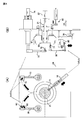
- FIG. 1 is a schematic diagram illustrating a configuration of a substrate processing apparatus according to an embodiment.
- FIG. 2 is a diagram showing in detail each of the coating unit 1 and the atmospheric transfer unit 2 shown in FIG.
- FIG. 3 shows the coating unit 1 shown in FIGS. 1 and 2 in detail.
- 4A is a plan view of the spin coater shown in FIG. 1
- FIG. 4B is a view of the spin coater shown in FIG. 5A is an SEM cross-sectional image of the 5 ⁇ m PZT thick film of the present invention (Example)
- FIG. 5B is an SEM cross-sectional image of the 5 ⁇ m PZT thick film of Conventional Example 1.
- FIG. 1 is a schematic diagram illustrating a configuration of a substrate processing apparatus according to an embodiment.
- FIG. 2 is a diagram showing in detail each of the coating unit 1 and the atmospheric transfer unit 2 shown in FIG.
- FIG. 3 shows the coating unit 1 shown in FIGS. 1 and 2 in detail.
- 4A is
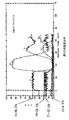
- FIGS. 6A and 6B are diagrams comparing the D-E hysteresis characteristics of the PZT thick film of the present invention (Example) and the PZT thick film of Conventional Example 1.
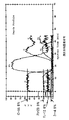
- FIG. FIGS. 7A and 7B are diagrams comparing the leakage current densities of the PZT thick film of the present invention (Example) and the PZT thick film of Conventional Example 1.
- FIG. 8A to 8C are diagrams showing the results of Raman spectroscopic analysis of the PZT thick film of the present invention (Example) and the PZT thick film of Conventional Example 1.
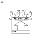
- FIG. FIG. 9 is a schematic diagram showing the concept of pressurized RTA.
- FIG. 10 is a diagram showing the concentration distribution in the depth direction of the PZT thick film of the present invention (Example) sintered with pressurized oxygen.
- FIG. 11 is a diagram showing the concentration distribution in the depth direction of the PZT thick film of Conventional Example 2 sintered with atmospheric pressure oxygen.
- FIG. 1 is a schematic diagram showing the configuration of the substrate processing apparatus according to the present embodiment.
- FIG. 2 is a diagram showing in detail each of the coating unit 1 and the atmospheric transfer unit 2 in the substrate processing apparatus shown in FIG.
- FIG. 3 shows the coating unit 1 shown in FIGS. 1 and 2 in detail.
- 4A is a plan view of the spin coater shown in FIG. 1, and FIG.
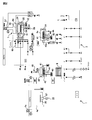
- the substrate processing apparatus has a coating unit 1 having a spin coater 4 and an atmospheric transfer unit 2 having a transfer chamber 2a.
- the coating unit 1 will be described in detail.
- the atmospheric transfer unit 2 will be described later.
- the coating unit 1 has an exhaust mechanism 1a that exhausts the inside of the coating unit 1 and the inside of the spin coat processing chamber 4a.
- the spin coater 4 includes a spin coat processing chamber 4a for applying a film on the substrate 20 by spin coating, a holding mechanism 21 for holding the substrate disposed in the spin coat processing chamber 4a, and a motor for rotating the substrate 20.
- the rotating mechanism 22 having The coating unit 1 is provided with an air conditioning mechanism that adjusts the amount of dust in the air in the spin coat processing chamber 4a.
- This air conditioning mechanism has a hepa filter. With this air conditioning mechanism, the amount of dust in the air in the spin coat processing chamber 4a can be reduced compared to the outside air. Note that this air conditioning mechanism can also control the temperature, humidity, or air volume in the spin coat processing chamber 4a.
- the holding mechanism 21 has a stage, and holds the back surface of the substrate placed on the stage by evacuating the vacuum pump DP. Connected to the holding mechanism 21 is a mechanism for releasing the atmosphere after the back surface of the substrate is evacuated. As shown in FIGS.
- the spin coater 4 has a cup 61 that covers the periphery of the substrate 20 held by the holding mechanism 21.
- a movement mechanism 62 having a cylinder is connected to the cup 61, and this movement mechanism 62 is a mechanism for moving the cup 61 up and down.
- the cup 61 is connected to a waste liquid tank 63 through a pipe, and this waste liquid tank 63 is a tank into which a liquid stored in the cup 61 is put by performing a spin coating process.
- the waste liquid tank 63 is connected to the waste liquid tank 64 via the pump P.
- the spin coater 4 has a cleaning nozzle 67, and the cleaning nozzle 67 is connected to a cleaning liquid supply source 66 through a valve and a pipe.
- the cleaning nozzle 67 is attached to the first swing arm 70, and the first swing arm 70 is configured to rotate by a motor (see FIG. 4A). Thereby, when supplying the cleaning liquid to the substrate 21, the cleaning nozzle 67 can be moved above the substrate.
- a cup 75 for receiving the cleaning liquid is disposed at the standby position of the cleaning nozzle 67.
- the cup 75 is connected to the waste liquid tank 63 via a pipe.
- the spin coater 4 has a blow nozzle 68, and this blow nozzle 68 is connected to a nitrogen gas supply source for pressure feeding and substrate blowing through a valve and piping.
- the blow nozzle 68 is attached to the first swing arm. Thereby, when supplying nitrogen gas to the surface of the substrate 21, the blow nozzle 68 can be moved above the substrate.
- the piping connecting the cleaning liquid supply source 66 and the cleaning nozzle 67 is configured so that the cleaning liquid is pressure-fed by nitrogen gas by connecting a nitrogen gas supply source for pressure feeding and substrate blowing through a valve.
- the spin coater 4 has a dripping nozzle 72, and this dripping nozzle 72 is connected to a chemical material supply source 71 through a pipe and a dispensing system 65.
- the dripping nozzle 72 is attached to a second swing arm 73, and the second swing arm 73 is configured to rotate by a motor 74 (see FIG. 4). Thereby, when supplying a chemical material to the board
- the dispensing system 65 is a system in which a chemical material is sent from a chemical material supply source 71 to a dropping nozzle 72 and dropped onto a substrate.
- the dispensing system 65 is connected to the waste liquid tank 63 via a pipe. Further, a vacuum pump DP is connected to the dispensing system 65 via a pipe.
- the dispensing system 65 is connected to a nitrogen gas supply source for pressure feeding and substrate blowing through piping and valves.
- a cup 76 that receives a chemical material is disposed at a standby position of the dropping nozzle 72, and a liquid level sensor that detects the liquid level in the cup is provided in the cup 76.
- the cup 76 is connected to the waste liquid tank 63 via a valve and piping.
- the cup 76 is connected to a cleaning liquid supply source 66 through piping and valves. Thereby, the dripping nozzle 72 can be cleaned with the cleaning liquid.
- the spin coater 4 has an edge rinse nozzle 77, and the edge rinse nozzle 77 is connected to a cleaning liquid supply source via a valve and a pipe.
- the edge rinse nozzle 77 is attached to the third swing arm 78.
- the third swing arm 78 is configured to rotate by a motor 79, and is configured to move up and down by a cylinder 80 (see FIG. 4). Thus, the edge rinse nozzle 77 can be moved above the substrate when supplying the cleaning liquid to the edge of the surface of the substrate 21.
- a cup 81 for receiving the cleaning liquid is disposed at the standby position of the edge rinse nozzle 77, and this cup 81 is connected to the waste liquid tank 63 via a pipe.
- the cup 61 is connected to a cleaning liquid supply source 66 through a pipe and a valve. Thereby, the cup 61 can be cleaned with the cleaning liquid.
- the spin coater 4 has a back surface rinsing nozzle 82 for rinsing the back surface of the substrate, and the back surface rinsing nozzle 82 is disposed in the cup 61.
- the back surface rinsing nozzle 82 is connected to the cleaning liquid supply source 66 through a pipe and a valve. Thereby, the back surface of the substrate can be cleaned with the cleaning liquid.
- the atmospheric transfer unit 2 includes a drying device 5 having a drying treatment chamber 5a for drying at a temperature of 150 ° C. to 300 ° C., a temperature of 300 to 600 ° C. in a nitrogen atmosphere or an inert gas atmosphere, Temporary nitrogen baking apparatus 6 having temporary nitrogen baking chamber 6a for temporary baking at normal pressure, pressurizing lamp annealing apparatus 7 having annealing chamber 7a, cooling apparatus 8 having cooling chamber, aligner 9 having alignment chamber A load / unload apparatus 10 having a load / unload chamber 10a and a transport mechanism 11 are disposed.
- the transfer chamber 2a of the atmospheric transfer unit 2 is connected to the spin coat processing chamber 4a via the gate valve 23, connected to the load / unload chamber 10a, connected to the alignment processing chamber, connected to the cooling processing chamber, and dried. It is connected to the processing chamber 5a, connected to the temporary baking processing chamber 6a via the gate valve 24, and connected to the annealing processing chamber 7a via the gate valve 25.
- the transport mechanism 11 of the atmospheric transport unit 2 includes a spin coat processing chamber 4a, a load / unload chamber 10a, an alignment processing chamber, a cooling processing chamber, a drying processing chamber 5a, a pre-baking processing chamber 6a, an annealing processing chamber 7a, and a loading chamber 12a.
- the atmospheric transfer unit 2 is provided with an air conditioning mechanism that adjusts the amount of dust in the air in the transfer chamber 2a.
- This air conditioning mechanism has a hepa filter (see FIG. 2). With this air conditioning mechanism, the amount of dust in the air in the transfer chamber 2a can be reduced compared to the outside air. In addition, this air-conditioning mechanism can also control the temperature or humidity in the transfer chamber 2a.
- the load / unload chamber 10 a of the load / unload apparatus 10 is for introducing or discharging a substrate into the atmospheric transfer unit 2.
- the alignment processing chamber of the aligner 9 is connected to the inside of the transfer chamber 2a and is a processing chamber for performing processing for detecting the center position of the surface of the substrate 20.
- the aligner 9 is provided with an air conditioning mechanism for adjusting the amount of dust in the air in the alignment processing chamber. Thereby, the amount of dust in the air in the alignment processing chamber can be reduced compared to the outside air. Note that this air conditioning mechanism can also control the temperature or humidity in the alignment processing chamber.
- the drying processing chamber 5 a of the drying device 5 is a processing chamber that performs a drying process on the film applied on the substrate by the spin coater 4. This drying process is a process for removing alcohol, moisture, and the like from the film, for example. As shown in FIG.
- a hot plate 42 for holding and heating the substrate 41 is disposed in the drying processing chamber 5a.
- a thermometer 43 is connected to the hot plate 42, and the hot plate 42 can be heated to a desired temperature (for example, 200 ° C.).
- the substrate 41 can be moved up and down by a lift 44 having pins.
- the drying device 5 has an exhaust mechanism 46 that exhausts the inside of the drying processing chamber 5a.
- the exhaust mechanism 46 has an exhaust port 45 disposed so as to face the substrate 41 held by the hot plate 42, and the air on the surface of the film coated on the substrate 41 is directly supplied from the exhaust port 45. Can be exhausted.
- the pre-baking treatment chamber 6a of the pre-baking apparatus 6 is a processing chamber for pre-baking a film applied on the substrate 41 at a desired temperature (for example, 300 ° C. to 600 ° C.) in a nitrogen atmosphere.
- a lamp heater 42 a for holding and heating the substrate 41 is disposed in the temporary baking apparatus 6.
- a thermometer 43 is connected to the lamp heater 42a, and the lamp heater 42a can be heated to a desired temperature.
- the substrate 41 can be moved up and down by a lift 44 having pins.
- the pre-baking apparatus 6 has a gas introduction mechanism for making the inside of the pre-baking treatment chamber 6a a predetermined atmosphere, and an exhaust system (such as a vacuum pump) for exhausting the inside of the pre-baking treatment chamber 6a.
- the gas introduction mechanism introduces nitrogen, for example.
- the pre-baking chamber 6a is connected to a nitrogen gas supply source, an oxygen gas supply source, or a dry air supply source via piping, valves, and a mass flow controller MFC1. Further, the inside of the pre-baking treatment chamber 6a can be depressurized to about 10 ⁇ 2 Pa by an exhaust system having a vacuum pump such as a dry pump.
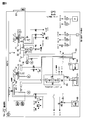
- the annealing chamber 7a of the pressurizing lamp annealing apparatus 7 is a processing chamber for performing a lamp annealing process on the film applied on the substrate at a temperature of 500 to 1000 ° C., for example. This lamp annealing treatment can be performed in any state of pressurization, normal pressure, and reduced pressure.
- the pressure-type lamp annealing apparatus 7 has an Al chamber 51, and the chamber 51 is configured to be water-cooled by a cooling mechanism (not shown).
- a mounting table 53 for mounting a substrate is provided in the chamber 51.
- the mounting table 53 is made of a material that transmits lamp light, for example, quartz.
- a quartz glass 54 is disposed above the mounting table 53.
- a lamp heater 55 is disposed on the quartz glass 54, and the lamp heater 55 is disposed inside a metal housing 56.
- An exhaust duct 57 is connected to the upper part of the housing 56, and the exhaust duct 57 exhausts heat in the housing 56.
- a window is provided in the lower part of the chamber 51 located below the mounting table 53, and calcium fluoride 58 is disposed in this window.
- a radiation thermometer 59 is disposed below the calcium fluoride 58.
- the calcium fluoride 58 is arranged to take in light in the wavelength region to be measured (infrared light having a wavelength of 5 ⁇ m).
- the present apparatus 7 has a thermometer 52 for measuring the temperature in the annealing chamber 7a.
- the annealing chamber 7a in the chamber 51 is connected to a pressurization line (pressurization mechanism) C2.
- the pressurization line C2 has a pressurization line using argon gas, a pressurization line using oxygen gas, and a pressurization line using nitrogen gas.
- the annealing chamber 7a in the chamber 1 is connected to a pressure adjustment line.
- the pressure adjusting line and the pressurizing line C2 can pressurize the annealing chamber 7a in the chamber 51 to a predetermined pressure (for example, less than 1 MPa).
- the pressure adjusting line includes a variable valve 69, and one side of the variable valve 69 is connected to the annealing chamber 7a via a pipe.
- the piping is connected to a pressure gauge DG, and the pressure inside the annealing chamber 7a can be measured by the pressure gauge DG.
- the other side of the variable valve 69 is connected to piping.
- the annealing chamber 7a is connected to a safety line.
- This safety line is for lowering the inside of the annealing chamber 7a to atmospheric pressure when the inside of the annealing chamber 7a is abnormally pressurized and becomes a certain pressure or higher.
- the safety line is equipped with an open valve.
- One side of the open valve is connected to the annealing chamber 7a via a pipe, and the other side of the open valve is connected to the pipe.
- the release valve allows gas to flow when a certain pressure is applied.
- the annealing chamber 7a is connected to an open air line. This air release line returns the inside of the annealing chamber 7a that has been normally pressurized to atmospheric pressure.
- the atmosphere open line is equipped with an open valve.
- One side of the open valve is connected to the annealing chamber 7a via a pipe, and the other side of the open valve is connected to the pipe.
- the opening valve is configured to gradually flow the gas in the annealing chamber 7a in order to return the annealing chamber 7a to atmospheric pressure.
- the annealing chamber 7a is connected to a line that returns the pressure from the reduced pressure state to the atmospheric pressure. This line returns the pressure from the reduced pressure state to the atmospheric pressure when the annealing chamber 7a is in a reduced pressure state (vacuum state).
- the line is equipped with a leak valve.
- One side of the leak valve is connected to the annealing chamber 7a via a pipe, and the other side of the leak valve is connected to a flow rate adjusting valve via the pipe.
- This flow rate adjusting valve is connected to a nitrogen gas supply source via a pipe. That is, the line returns the atmospheric pressure inside the annealing chamber 7a by gradually introducing nitrogen gas into the annealing chamber 7a from the nitrogen gas supply source through the flow rate adjusting valve and the leak valve. .
- the annealing chamber 7a is connected to a vacuum exhaust line for reducing the pressure inside the chamber 7a.
- the evacuation line has a valve, and one end of the valve is connected to the annealing chamber 7a through a pipe. The other end of the valve is connected to a vacuum pump via a pipe.
- This evacuation line is used, for example, when evacuating once before performing pressurized RTA.
- Each of the casing 56 and the lamp heater 55 is connected to a dry air supply source A2 through a pipe.
- the cooling processing chamber of the cooling device 8 is a processing chamber for cooling a substrate on which a drying process, a temporary baking process, a lamp annealing process, or the like has been performed.
- bulb mentioned above is connected to the compressed air supply source for valve drive via piping.
- Each of the alignment processing chamber of the aligner 9 and the transfer chamber 2a of the atmospheric transfer unit 2 is connected to the vacuum pump DP2 via a pipe.
- This thin film is a ferroelectric film such as a PZT film.
- the amount of dust in the air is adjusted in the transfer chamber 2a by the air conditioning mechanism, and the amount of dust in the air is adjusted in the alignment processing chamber by the air conditioning mechanism.
- processing for detecting the center position of the surface of the substrate is performed in the alignment processing chamber. This processing is performed in order to detect the center position of the substrate surface and to match the center position of the substrate surface with the rotation center of the substrate when performing the spin coating process.
- the gate valve 23 of the spin coat processing chamber 4a is opened, and the substrate in the alignment processing chamber is transferred into the spin coat processing chamber 4a through the transfer chamber 2a by the transfer mechanism 11, and this substrate is transferred to the spin coat processing chamber 4a.
- the gate valve 23 is closed by the holding mechanism 21 inside.
- the amount of dust in the air is adjusted in the spin coat processing chamber 4a by an air conditioning mechanism. Thereafter, a step of applying a film by spin coating on the substrate in the spin coat processing chamber 4a is performed.
- This process will be described in detail below.
- the substrate is rotated while supplying the cleaning liquid onto the substrate by the cleaning nozzle 67. Thereby, the surface of the substrate is cleaned.
- the supply of the cleaning liquid is stopped, and the cleaning liquid on the substrate is removed by rotating the substrate.
- the substrate is rotated while dropping the chemical material onto the substrate by the dropping nozzle 72.
- the cleaning liquid is dropped onto the edge of the substrate surface by the edge rinse nozzle 77. Thereby, a chemical material film is applied on the substrate.
- the cleaning liquid is dropped on the edge of the substrate surface is that when the film is applied onto the substrate by spin coating, the film thickness at the edge of the substrate is formed thicker than the center of the substrate. This is to apply while removing. Accordingly, it is preferable to move the edge of the cleaning liquid gradually from the end of the substrate toward the center by moving the edge rinse nozzle 77 gradually from the end of the substrate toward the center.
- the chemical material is supplied onto the substrate from one chemical material supply source 71.
- a plurality of chemical material supply sources are arranged and a plurality of materials are mixed in a predetermined manner. You may supply the chemical material mixed by ratio on a board
- the gate valve 23 of the spin coat processing chamber 4a is opened, and the substrate in the spin coat processing chamber 4a is transferred into the drying processing chamber 5a through the transfer chamber 2a by the transfer mechanism 11, and this substrate is transferred to the drying processing chamber. Holding by the holding mechanism in 5a, the gate valve 23 is closed. Then, the process which performs a drying process to the chemical material film
- the substrate is heated to, for example, 200 to 250 ° C.
- the gate valve 24 of the pre-baking chamber 6a is opened, the substrate in the drying chamber is transferred by the transfer mechanism 11 into the pre-baking chamber 6a through the transfer chamber 2a, and this substrate is transferred to the pre-baking chamber 6a.
- the gate valve 24 is closed by the holding mechanism inside. Thereafter, a process of pre-baking the chemical material film on the substrate in the pre-baking chamber 6a is performed.
- the inside of the pre-baking treatment chamber 6a is evacuated by an exhaust system, the inside of the pre-baking treatment chamber 6a is set to a normal pressure in a vacuum atmosphere, a nitrogen atmosphere or an inert gas atmosphere by a gas introduction mechanism, Temporary baking is performed by heating the chemical material film on the substrate to a desired temperature (for example, 300 ° C. to 600 ° C.). Thereafter, the gate valve 24 is opened, and the substrate in the temporary baking chamber 6a is transferred by the transfer mechanism 11 into the cooling processing chamber of the cooling device 8 through the transfer chamber 2a, and this substrate is transferred by the holding mechanism in the cooling chamber. Hold and close the gate valve 24. Thereafter, the substrate is cooled to a predetermined temperature in the cooling processing chamber.
- a desired temperature for example, 300 ° C. to 600 ° C.
- the substrate in the cooling processing chamber is transferred by the transfer mechanism 11 to the alignment processing chamber of the aligner 9 through the transfer chamber 2a, and this substrate is processed to detect the center position of the surface of the substrate in the alignment processing chamber.
- the gate valve 23 of the spin coat processing chamber 4a is opened, and the substrate in the alignment processing chamber is transferred into the spin coat processing chamber 4a through the transfer chamber 2a by the transfer mechanism 11, and this substrate is transferred to the spin coat processing chamber 4a.
- the gate valve 23 is closed by the holding mechanism 21 inside.
- a plurality of chemical material films are stacked on the substrate by repeating the spin coating process, the drying process, and the pre-baking process a plurality of times (for example, 30 times).
- a thicker film for example, a film thickness of 1 ⁇ m or more
- productivity can be improved by using the substrate processing apparatus described above.
- the spin coat process, the drying process, and the pre-baking process can be automatically performed by operating the substrate processing apparatus as described above by the control unit (not shown). For this reason, it is conceivable that each process is performed individually, and if the operator transports the substrate by hand, the hands may be numb, the processing order may be wrong, or the substrate may be dropped during transport, but this does not happen. There is an advantage. Therefore, productivity can be improved in mass production, and yield can be increased.
- the gate valve 24 of the pre-baking treatment chamber 6a is opened, the gate valve 25 of the pressure-type lamp annealing apparatus 7 is opened, and the substrate in the pre-baking treatment chamber 6a is annealed by the transfer mechanism 11 through the transfer chamber 2a.
- the substrate is transferred into the chamber 7a, the substrate is held by a holding mechanism, and the gate valves 24 and 25 are closed.
- the transfer time for transferring the substrate from the pre-baking chamber 6a to the annealing chamber 7a is 10 seconds or less. The reason for shortening the conveyance time in this way is as follows. If the transport time is long, the characteristics of the ferroelectric film are greatly affected.
- the chemical material film has a very high oxygen activity and is in an oxygen-deficient state, so that it is combined with oxygen in the atmosphere and the film characteristics deteriorate. Therefore, it is preferable to shorten the conveyance time.
- a lamp annealing process is performed on the plurality of layers of chemical material films on the substrate in the annealing chamber 7a.
- the annealing chamber 7a is set to a predetermined pressure (pressurization, normal pressure or reduced pressure) in a predetermined atmosphere, and the lamp material 55 is used to heat the chemical material film on the substrate to a desired temperature.
- the chemical material film is a ferroelectric film
- the ferroelectric film is crystallized by annealing.
- the substrate in the annealing chamber 7a is transferred by the transfer mechanism 11 into the load / unload chamber 10a through the transfer chamber 2a, and the substrate is unloaded.
- a thin film is produced on a substrate using the substrate processing apparatus shown in FIGS.
- the coating amount per one time was 500 uL, and the PZT thick film coating was performed on the substrate using the following spin conditions. Increase to 0-300 rpm in 3 seconds, hold for 3 seconds, then increase to 300-500 rpm for 5 seconds, hold for 5 seconds, then increase to 500-1500 rpm for 5 seconds Raise and hold for 90 seconds.
- the substrate was held for 30 seconds on a hot plate heated to 250 ° C., and moisture was removed from the applied PZT thick film.
- the temporary baking process was performed to the sample given to said drying process. Specifically, evacuation of the pre-baking chamber 6a was performed with a rotary pump, and the ultimate vacuum was set to 10 ⁇ 1 Pa.
- the inside of the pre-baking chamber 6a was filled with N 2 to atmospheric pressure, and the substrate was heated at 450 ° C. for 90 seconds to decompose and remove organic components.
- a pre-baking step different from that of the present example was performed on the sample subjected to the above drying step.
- pre-baking was performed at 450 ° C. for 90 seconds in atmospheric air (containing oxygen).
- This sample is referred to as Conventional Example 1.
- the above-described spin coating, drying step, and pre-baking step were repeated 15 times to produce samples (Example and Conventional Example 1) in which a PZT thick film having a total film thickness of 5 ⁇ m was formed on the substrate.
- the PZT thick film was crystallized by performing a lamp annealing treatment on the 5 ⁇ m thick PZT film on each substrate of the above samples (Example and Conventional Example 1) using a rapid heating apparatus (RTA).
- RTA rapid heating apparatus
- the PZT thick film of this example is heated to a temperature of 700 ° C.
- FIG. 5B is an SEM cross-sectional image of the conventional 5 ⁇ m PZT thick film.
- FIG. 6A is a diagram showing the results of the hysteresis evaluation of the 5 ⁇ m PZT thick film of the present invention (Example), and FIG. 6B is the hysteresis evaluation of the 5 ⁇ m PZT thick film of Conventional Example 1. It is a figure which shows a result. As shown in FIG. 6A, in the present invention (Example), good hysteresis was obtained, whereas in Conventional Example 1, as shown in FIG. 6B, a very distorted small hysteresis curve and became.
- FIG. 6A is a diagram showing the results of the hysteresis evaluation of the 5 ⁇ m PZT thick film of the present invention (Example)
- FIG. 6B is the hysteresis evaluation of the 5 ⁇ m PZT thick film of Conventional Example 1. It is a figure which shows
- FIG. 7A is a diagram showing the result of measuring the leakage current density for the 5 ⁇ m PZT thick film of the present invention (Example), and FIG. 7B is the leakage current for the 5 ⁇ m PZT thick film of Conventional Example 1. It is a figure which shows the result of having measured the density. As shown in FIG. 7 (A), the present invention showed good leak characteristics, whereas as shown in FIG. 7 (B), Conventional Example 1 has 10 ⁇ 6 to 10 ⁇ 3 A / cm 2 . A very large leakage current was observed.
- FIG. 8A is a diagram showing the results of Raman spectroscopic analysis of the 5 ⁇ m PZT thick film of the present invention (Example), and FIG.
- FIG. 8B is the result of Raman spectroscopic analysis of the 5 ⁇ m PZT thick film of Conventional Example 1.
- FIG. 8C is an enlarged view of B shown in FIG. 8B.
- the pressurized RTA was further examined in detail. The concept of the pressurized RTA is as shown in FIG. Specifically, PZT crystal initial nuclei are generated by excess lead, but since the PZT crystal itself is stoichiometry, excess lead accumulated in the upper part of the thin film with pressurized oxygen is removed by accelerating oxidation with pressurized oxygen. .
- Pb Zr + Ti
- FIG. 10 and FIG. 11 show that Conventional Example 2 contains more oxygen.
- Conventional Example 2 contains more oxygen than the PZT thick film of the present invention. This is thought to be because the Pb component, which is often observed in Conventional Example 2, is present at the PZT grain boundary as an impurity called PbOx.
Landscapes
- Engineering & Computer Science (AREA)
- Microelectronics & Electronic Packaging (AREA)
- Condensed Matter Physics & Semiconductors (AREA)
- General Physics & Mathematics (AREA)
- Manufacturing & Machinery (AREA)
- Computer Hardware Design (AREA)
- Physics & Mathematics (AREA)
- Power Engineering (AREA)
- Chemical & Material Sciences (AREA)
- Materials Engineering (AREA)
- Formation Of Insulating Films (AREA)
- Semiconductor Memories (AREA)
- Coating Apparatus (AREA)
Abstract
La présente invention concerne un appareil de traitement de substrat permettant de supprimer l'adhésion de poussières sur un film appliqué sur un substrat. L'appareil de traitement de substrat comprend : une chambre de dépôt à la tournette (4a), dans laquelle le film est appliqué sur le substrat par dépôt à la tournette ; un premier mécanisme de conditionnement d'air, qui règle la quantité de poussières dans l'air dans la chambre de dépôt à la tournette ; une chambre de recuit (7a), dans laquelle le film appliqué sur le substrat est recuit par lampe ; une chambre de transfert (2a), qui est raccordée à la chambre de dépôt à la tournette et à la chambre de recuit, et qui transfère le substrat entre la chambre de dépôt à la tournette et la chambre de recuit ; et un second mécanisme de conditionnement d'air, qui règle la quantité de poussières dans l'air dans la chambre de transfert.
Priority Applications (5)
| Application Number | Priority Date | Filing Date | Title |
|---|---|---|---|
| PCT/JP2010/057919 WO2011135731A1 (fr) | 2010-04-28 | 2010-04-28 | Appareil de traitement de substrat, et procédé de fabrication de film mince |
| EP10850746.8A EP2565910A4 (fr) | 2010-04-28 | 2010-04-28 | Appareil de traitement de substrat, et procédé de fabrication de film mince |
| US13/643,873 US9171745B2 (en) | 2010-04-28 | 2010-04-28 | Substrate treatment apparatus and method for manufacturing thin film |
| JP2012512616A JP5699297B2 (ja) | 2010-04-28 | 2010-04-28 | 基板処理装置及び薄膜の製造方法 |
| TW100113724A TWI523132B (zh) | 2010-04-28 | 2011-04-20 | Substrate processing apparatus and method for manufacturing the same |
Applications Claiming Priority (1)
| Application Number | Priority Date | Filing Date | Title |
|---|---|---|---|
| PCT/JP2010/057919 WO2011135731A1 (fr) | 2010-04-28 | 2010-04-28 | Appareil de traitement de substrat, et procédé de fabrication de film mince |
Publications (1)
| Publication Number | Publication Date |
|---|---|
| WO2011135731A1 true WO2011135731A1 (fr) | 2011-11-03 |
Family
ID=44861069
Family Applications (1)
| Application Number | Title | Priority Date | Filing Date |
|---|---|---|---|
| PCT/JP2010/057919 WO2011135731A1 (fr) | 2010-04-28 | 2010-04-28 | Appareil de traitement de substrat, et procédé de fabrication de film mince |
Country Status (5)
| Country | Link |
|---|---|
| US (1) | US9171745B2 (fr) |
| EP (1) | EP2565910A4 (fr) |
| JP (1) | JP5699297B2 (fr) |
| TW (1) | TWI523132B (fr) |
| WO (1) | WO2011135731A1 (fr) |
Cited By (5)
| Publication number | Priority date | Publication date | Assignee | Title |
|---|---|---|---|---|
| JP2013211306A (ja) * | 2012-03-30 | 2013-10-10 | Mitsubishi Materials Corp | Pzt系強誘電体薄膜の製造方法 |
| JP2015026693A (ja) * | 2013-07-25 | 2015-02-05 | 株式会社ユーテック | 膜の製造方法及びマルチチャンバー装置 |
| WO2015045980A1 (fr) * | 2013-09-26 | 2015-04-02 | 株式会社 アルバック | Dispositif de traitement de substrat et dispositif de formation de film |
| JP2016540625A (ja) * | 2013-10-11 | 2016-12-28 | トランジションズ オプティカル, インコーポレイテッド | 光学基材に複数コーティングを塗布するためのスピンコーター |
| US10741421B2 (en) | 2017-09-05 | 2020-08-11 | Toshiba Memory Corporation | Semiconductor manufacturing apparatus |
Families Citing this family (4)
| Publication number | Priority date | Publication date | Assignee | Title |
|---|---|---|---|---|
| JP6001896B2 (ja) | 2012-03-27 | 2016-10-05 | 株式会社Screenセミコンダクターソリューションズ | 基板洗浄装置およびそれを備えた基板処理装置 |
| US20140087073A1 (en) * | 2012-09-24 | 2014-03-27 | Igor Constantin Ivanov | Equipment and method of manufacturing for liquid processing in a controlled atmospheric ambient |
| KR102677969B1 (ko) * | 2020-12-30 | 2024-06-26 | 세메스 주식회사 | 노즐 대기 포트와 이를 포함하는 기판 처리 장치 및 이를 이용한 노즐 세정 방법 |
| JP2022124070A (ja) * | 2021-02-15 | 2022-08-25 | 株式会社Screenホールディングス | 基板処理装置、および、筒状ガードの加工方法 |
Citations (8)
| Publication number | Priority date | Publication date | Assignee | Title |
|---|---|---|---|---|
| JPH11145424A (ja) * | 1997-11-14 | 1999-05-28 | Fujitsu Ltd | 強誘電体薄膜の形成方法 |
| JP2000009434A (ja) * | 1998-06-24 | 2000-01-14 | Matsushita Electric Ind Co Ltd | 光学式リニアセンサによる計測方法 |
| JP2000114345A (ja) * | 1998-09-30 | 2000-04-21 | Ebara Corp | 基板の位置決め装置 |
| JP2004319995A (ja) * | 2003-03-28 | 2004-11-11 | Seiko Epson Corp | 強誘電体膜およびその製造方法ならびに半導体装置 |
| WO2006087777A1 (fr) | 2005-02-16 | 2006-08-24 | Youtec Co., Ltd. | Dispositif de recuit de lampe de pressurisation, procédé de recuit de lampe de pressurisation, film mince et composante électronique |
| JP2007059631A (ja) * | 2005-08-24 | 2007-03-08 | Tokyo Electron Ltd | ABOx型ペロブスカイト結晶構造の誘電体薄膜の形成装置及び形成方法 |
| JP2007180398A (ja) * | 2005-12-28 | 2007-07-12 | Tdk Corp | コンデンサの製造方法 |
| JP2007329030A (ja) * | 2006-06-08 | 2007-12-20 | Sumitomo Metal Mining Co Ltd | 高誘電体膜形成用組成物とその製造方法 |
Family Cites Families (5)
| Publication number | Priority date | Publication date | Assignee | Title |
|---|---|---|---|---|
| JP4543617B2 (ja) | 2002-04-22 | 2010-09-15 | セイコーエプソン株式会社 | アクティブマトリクス基板の製造方法、電気光学装置の製造方法、電子機器の製造方法、アクティブマトリクス基板の製造装置、電気光学装置の製造装置、及び電気機器の製造装置 |
| JP2007073670A (ja) * | 2005-09-06 | 2007-03-22 | Disco Abrasive Syst Ltd | 水溶性樹脂被覆方法 |
| US8322299B2 (en) * | 2006-05-17 | 2012-12-04 | Taiwan Semiconductor Manufacturing Co., Ltd. | Cluster processing apparatus for metallization processing in semiconductor manufacturing |
| US20090056116A1 (en) * | 2007-08-07 | 2009-03-05 | Micro Foundry Inc. | Integrated miniature device factory |
| US7803720B2 (en) * | 2008-01-25 | 2010-09-28 | Kabushiki Kaisha Toshiba | Coating process and equipment for reduced resist consumption |
-
2010
- 2010-04-28 US US13/643,873 patent/US9171745B2/en active Active
- 2010-04-28 EP EP10850746.8A patent/EP2565910A4/fr not_active Withdrawn
- 2010-04-28 WO PCT/JP2010/057919 patent/WO2011135731A1/fr active Application Filing
- 2010-04-28 JP JP2012512616A patent/JP5699297B2/ja active Active
-
2011
- 2011-04-20 TW TW100113724A patent/TWI523132B/zh active
Patent Citations (8)
| Publication number | Priority date | Publication date | Assignee | Title |
|---|---|---|---|---|
| JPH11145424A (ja) * | 1997-11-14 | 1999-05-28 | Fujitsu Ltd | 強誘電体薄膜の形成方法 |
| JP2000009434A (ja) * | 1998-06-24 | 2000-01-14 | Matsushita Electric Ind Co Ltd | 光学式リニアセンサによる計測方法 |
| JP2000114345A (ja) * | 1998-09-30 | 2000-04-21 | Ebara Corp | 基板の位置決め装置 |
| JP2004319995A (ja) * | 2003-03-28 | 2004-11-11 | Seiko Epson Corp | 強誘電体膜およびその製造方法ならびに半導体装置 |
| WO2006087777A1 (fr) | 2005-02-16 | 2006-08-24 | Youtec Co., Ltd. | Dispositif de recuit de lampe de pressurisation, procédé de recuit de lampe de pressurisation, film mince et composante électronique |
| JP2007059631A (ja) * | 2005-08-24 | 2007-03-08 | Tokyo Electron Ltd | ABOx型ペロブスカイト結晶構造の誘電体薄膜の形成装置及び形成方法 |
| JP2007180398A (ja) * | 2005-12-28 | 2007-07-12 | Tdk Corp | コンデンサの製造方法 |
| JP2007329030A (ja) * | 2006-06-08 | 2007-12-20 | Sumitomo Metal Mining Co Ltd | 高誘電体膜形成用組成物とその製造方法 |
Non-Patent Citations (1)
| Title |
|---|
| See also references of EP2565910A4 |
Cited By (7)
| Publication number | Priority date | Publication date | Assignee | Title |
|---|---|---|---|---|
| JP2013211306A (ja) * | 2012-03-30 | 2013-10-10 | Mitsubishi Materials Corp | Pzt系強誘電体薄膜の製造方法 |
| JP2015026693A (ja) * | 2013-07-25 | 2015-02-05 | 株式会社ユーテック | 膜の製造方法及びマルチチャンバー装置 |
| WO2015045980A1 (fr) * | 2013-09-26 | 2015-04-02 | 株式会社 アルバック | Dispositif de traitement de substrat et dispositif de formation de film |
| JP6009685B2 (ja) * | 2013-09-26 | 2016-10-19 | 株式会社アルバック | 基板処理装置、および、成膜装置 |
| JP2016540625A (ja) * | 2013-10-11 | 2016-12-28 | トランジションズ オプティカル, インコーポレイテッド | 光学基材に複数コーティングを塗布するためのスピンコーター |
| US10571611B2 (en) | 2013-10-11 | 2020-02-25 | Transitions Optical, Inc. | Spin coater for applying multiple coatings to an optical substrate |
| US10741421B2 (en) | 2017-09-05 | 2020-08-11 | Toshiba Memory Corporation | Semiconductor manufacturing apparatus |
Also Published As
| Publication number | Publication date |
|---|---|
| JPWO2011135731A1 (ja) | 2013-07-18 |
| TW201205709A (en) | 2012-02-01 |
| EP2565910A1 (fr) | 2013-03-06 |
| TWI523132B (zh) | 2016-02-21 |
| US20130059076A1 (en) | 2013-03-07 |
| EP2565910A4 (fr) | 2014-01-15 |
| US9171745B2 (en) | 2015-10-27 |
| JP5699297B2 (ja) | 2015-04-08 |
Similar Documents
| Publication | Publication Date | Title |
|---|---|---|
| JP5699297B2 (ja) | 基板処理装置及び薄膜の製造方法 | |
| KR101847575B1 (ko) | 기판 처리 장치, 반도체 장치의 제조 방법 및 기록 매체 | |
| JP6282672B2 (ja) | 基板を自然に酸化する方法およびシステム | |
| KR101177366B1 (ko) | 반도체 장치의 제조 방법 및 기판 처리 장치 | |
| US8481434B2 (en) | Method of manufacturing a semiconductor device and processing apparatus | |
| KR101232688B1 (ko) | 기판 처리 장치 및 반도체 장치의 제조 방법 및 액체 유량 제어 장치의 동작 확인 방법 | |
| JP5902073B2 (ja) | 半導体装置の製造方法、基板処理方法及び基板処理装置 | |
| US20130247937A1 (en) | Substrate processing apparatus and its maintenance method, substrate transfer method and program | |
| JP3741604B2 (ja) | 熱処理装置および熱処理方法 | |
| KR20110002428A (ko) | 반도체 장치의 제조 방법 및 기판 처리 시스템 | |
| JP5208294B2 (ja) | 半導体装置の製造方法、基板処理方法及び基板処理装置 | |
| US9966283B2 (en) | Pressurizing-type lamp annealing device, method for producing thin film, and method for using pressurizing-type lamp annealing device | |
| JP2011249407A (ja) | 基板処理装置 | |
| JP3739287B2 (ja) | 減圧乾燥方法及び塗布膜形成装置 | |
| JP2015026693A (ja) | 膜の製造方法及びマルチチャンバー装置 | |
| JP5246843B2 (ja) | 基板処理装置、ベーキング方法及び半導体装置の製造方法 | |
| JP4563113B2 (ja) | シリコン酸化膜の形成方法、半導体デバイスの製造方法および基板処理装置 | |
| JP5350329B2 (ja) | 半導体デバイスの製造方法および基板処理装置 | |
| JP6789171B2 (ja) | 基板処理装置、処理ガスノズル内のパーティクルコーティング方法及び基板処理方法 | |
| JP2013089911A (ja) | 基板処理装置および半導体装置の製造方法 | |
| JP2010212391A (ja) | 半導体装置の製造方法及び基板処理装置 | |
| JP2012009744A (ja) | 基板処理装置 | |
| JP2011222656A (ja) | 基板処理装置 | |
| WO2020196025A1 (fr) | Dispositif de traitement de substrat, procédé de fabrication de dispositif à semi-conducteur, et outil de support de substrat et procédé de traitement de celui-ci | |
| JP4503713B2 (ja) | 真空成膜法の基板冷却方法 |
Legal Events
| Date | Code | Title | Description |
|---|---|---|---|
| 121 | Ep: the epo has been informed by wipo that ep was designated in this application |
Ref document number: 10850746 Country of ref document: EP Kind code of ref document: A1 |
|
| WWE | Wipo information: entry into national phase |
Ref document number: 2012512616 Country of ref document: JP |
|
| WWE | Wipo information: entry into national phase |
Ref document number: 2010850746 Country of ref document: EP |
|
| NENP | Non-entry into the national phase |
Ref country code: DE |
|
| WWE | Wipo information: entry into national phase |
Ref document number: 13643873 Country of ref document: US |