WO2011125878A1 - 光電変換装置及び光電変換装置の製造方法 - Google Patents
光電変換装置及び光電変換装置の製造方法 Download PDFInfo
- Publication number
- WO2011125878A1 WO2011125878A1 PCT/JP2011/058289 JP2011058289W WO2011125878A1 WO 2011125878 A1 WO2011125878 A1 WO 2011125878A1 JP 2011058289 W JP2011058289 W JP 2011058289W WO 2011125878 A1 WO2011125878 A1 WO 2011125878A1
- Authority
- WO
- WIPO (PCT)
- Prior art keywords
- photoelectric conversion
- layer
- semiconductor layer
- conversion unit
- type semiconductor
- Prior art date
- Legal status (The legal status is an assumption and is not a legal conclusion. Google has not performed a legal analysis and makes no representation as to the accuracy of the status listed.)
- Ceased
Links
Images



Classifications
-
- H—ELECTRICITY
- H10—SEMICONDUCTOR DEVICES; ELECTRIC SOLID-STATE DEVICES NOT OTHERWISE PROVIDED FOR
- H10F—INORGANIC SEMICONDUCTOR DEVICES SENSITIVE TO INFRARED RADIATION, LIGHT, ELECTROMAGNETIC RADIATION OF SHORTER WAVELENGTH OR CORPUSCULAR RADIATION
- H10F71/00—Manufacture or treatment of devices covered by this subclass
- H10F71/10—Manufacture or treatment of devices covered by this subclass the devices comprising amorphous semiconductor material
- H10F71/103—Manufacture or treatment of devices covered by this subclass the devices comprising amorphous semiconductor material including only Group IV materials
-
- H—ELECTRICITY
- H10—SEMICONDUCTOR DEVICES; ELECTRIC SOLID-STATE DEVICES NOT OTHERWISE PROVIDED FOR
- H10F—INORGANIC SEMICONDUCTOR DEVICES SENSITIVE TO INFRARED RADIATION, LIGHT, ELECTROMAGNETIC RADIATION OF SHORTER WAVELENGTH OR CORPUSCULAR RADIATION
- H10F10/00—Individual photovoltaic cells, e.g. solar cells
- H10F10/10—Individual photovoltaic cells, e.g. solar cells having potential barriers
- H10F10/17—Photovoltaic cells having only PIN junction potential barriers
- H10F10/172—Photovoltaic cells having only PIN junction potential barriers comprising multiple PIN junctions, e.g. tandem cells
-
- H—ELECTRICITY
- H10—SEMICONDUCTOR DEVICES; ELECTRIC SOLID-STATE DEVICES NOT OTHERWISE PROVIDED FOR
- H10F—INORGANIC SEMICONDUCTOR DEVICES SENSITIVE TO INFRARED RADIATION, LIGHT, ELECTROMAGNETIC RADIATION OF SHORTER WAVELENGTH OR CORPUSCULAR RADIATION
- H10F71/00—Manufacture or treatment of devices covered by this subclass
- H10F71/121—The active layers comprising only Group IV materials
-
- H—ELECTRICITY
- H10—SEMICONDUCTOR DEVICES; ELECTRIC SOLID-STATE DEVICES NOT OTHERWISE PROVIDED FOR
- H10F—INORGANIC SEMICONDUCTOR DEVICES SENSITIVE TO INFRARED RADIATION, LIGHT, ELECTROMAGNETIC RADIATION OF SHORTER WAVELENGTH OR CORPUSCULAR RADIATION
- H10F77/00—Constructional details of devices covered by this subclass
- H10F77/10—Semiconductor bodies
- H10F77/16—Material structures, e.g. crystalline structures, film structures or crystal plane orientations
- H10F77/162—Non-monocrystalline materials, e.g. semiconductor particles embedded in insulating materials
- H10F77/164—Polycrystalline semiconductors
- H10F77/1642—Polycrystalline semiconductors including only Group IV materials
- H10F77/1645—Polycrystalline semiconductors including only Group IV materials including microcrystalline silicon
-
- H—ELECTRICITY
- H10—SEMICONDUCTOR DEVICES; ELECTRIC SOLID-STATE DEVICES NOT OTHERWISE PROVIDED FOR
- H10F—INORGANIC SEMICONDUCTOR DEVICES SENSITIVE TO INFRARED RADIATION, LIGHT, ELECTROMAGNETIC RADIATION OF SHORTER WAVELENGTH OR CORPUSCULAR RADIATION
- H10F77/00—Constructional details of devices covered by this subclass
- H10F77/10—Semiconductor bodies
- H10F77/16—Material structures, e.g. crystalline structures, film structures or crystal plane orientations
- H10F77/162—Non-monocrystalline materials, e.g. semiconductor particles embedded in insulating materials
- H10F77/166—Amorphous semiconductors
- H10F77/1662—Amorphous semiconductors including only Group IV materials
-
- Y—GENERAL TAGGING OF NEW TECHNOLOGICAL DEVELOPMENTS; GENERAL TAGGING OF CROSS-SECTIONAL TECHNOLOGIES SPANNING OVER SEVERAL SECTIONS OF THE IPC; TECHNICAL SUBJECTS COVERED BY FORMER USPC CROSS-REFERENCE ART COLLECTIONS [XRACs] AND DIGESTS
- Y02—TECHNOLOGIES OR APPLICATIONS FOR MITIGATION OR ADAPTATION AGAINST CLIMATE CHANGE
- Y02E—REDUCTION OF GREENHOUSE GAS [GHG] EMISSIONS, RELATED TO ENERGY GENERATION, TRANSMISSION OR DISTRIBUTION
- Y02E10/00—Energy generation through renewable energy sources
- Y02E10/50—Photovoltaic [PV] energy
- Y02E10/545—Microcrystalline silicon PV cells
-
- Y—GENERAL TAGGING OF NEW TECHNOLOGICAL DEVELOPMENTS; GENERAL TAGGING OF CROSS-SECTIONAL TECHNOLOGIES SPANNING OVER SEVERAL SECTIONS OF THE IPC; TECHNICAL SUBJECTS COVERED BY FORMER USPC CROSS-REFERENCE ART COLLECTIONS [XRACs] AND DIGESTS
- Y02—TECHNOLOGIES OR APPLICATIONS FOR MITIGATION OR ADAPTATION AGAINST CLIMATE CHANGE
- Y02E—REDUCTION OF GREENHOUSE GAS [GHG] EMISSIONS, RELATED TO ENERGY GENERATION, TRANSMISSION OR DISTRIBUTION
- Y02E10/00—Energy generation through renewable energy sources
- Y02E10/50—Photovoltaic [PV] energy
- Y02E10/547—Monocrystalline silicon PV cells
-
- Y—GENERAL TAGGING OF NEW TECHNOLOGICAL DEVELOPMENTS; GENERAL TAGGING OF CROSS-SECTIONAL TECHNOLOGIES SPANNING OVER SEVERAL SECTIONS OF THE IPC; TECHNICAL SUBJECTS COVERED BY FORMER USPC CROSS-REFERENCE ART COLLECTIONS [XRACs] AND DIGESTS
- Y02—TECHNOLOGIES OR APPLICATIONS FOR MITIGATION OR ADAPTATION AGAINST CLIMATE CHANGE
- Y02E—REDUCTION OF GREENHOUSE GAS [GHG] EMISSIONS, RELATED TO ENERGY GENERATION, TRANSMISSION OR DISTRIBUTION
- Y02E10/00—Energy generation through renewable energy sources
- Y02E10/50—Photovoltaic [PV] energy
- Y02E10/548—Amorphous silicon PV cells
-
- Y—GENERAL TAGGING OF NEW TECHNOLOGICAL DEVELOPMENTS; GENERAL TAGGING OF CROSS-SECTIONAL TECHNOLOGIES SPANNING OVER SEVERAL SECTIONS OF THE IPC; TECHNICAL SUBJECTS COVERED BY FORMER USPC CROSS-REFERENCE ART COLLECTIONS [XRACs] AND DIGESTS
- Y02—TECHNOLOGIES OR APPLICATIONS FOR MITIGATION OR ADAPTATION AGAINST CLIMATE CHANGE
- Y02P—CLIMATE CHANGE MITIGATION TECHNOLOGIES IN THE PRODUCTION OR PROCESSING OF GOODS
- Y02P70/00—Climate change mitigation technologies in the production process for final industrial or consumer products
- Y02P70/50—Manufacturing or production processes characterised by the final manufactured product
Definitions
- the present invention relates to a photoelectric conversion device and a method for manufacturing the photoelectric conversion device.
- This application claims priority based on Japanese Patent Application No. 2010-086181 filed in Japan on April 2, 2010, the contents of which are incorporated herein by reference.
- a photoelectric conversion device using single crystal silicon is excellent in energy conversion efficiency per unit area.
- a photoelectric conversion device using single crystal silicon uses a silicon wafer obtained by slicing a single crystal silicon ingot, a large amount of energy is consumed for manufacturing the ingot and the manufacturing cost is high.
- a photoelectric conversion device using an amorphous (amorphous) silicon thin film hereinafter also referred to as “a-Si thin film” that can be manufactured at a lower cost is widely used as a low-cost photoelectric conversion device.
- a tandem structure in which two photoelectric conversion units are stacked has been proposed as a structure for improving the conversion efficiency of the photoelectric conversion device.
- a tandem photoelectric conversion device 200 as shown in FIG. 7 is known.
- an insulating transparent substrate 201 provided with a transparent conductive film 202 is used.
- a pin-type first photoelectric conversion unit 203 obtained by sequentially stacking a p-type semiconductor layer 231, an i-type silicon layer (amorphous silicon layer) 232, and an n-type semiconductor layer 233 on the transparent conductive film 202. Is formed.
- a pin-type second photoelectric conversion unit obtained by sequentially stacking a p-type semiconductor layer 241, an i-type silicon layer (crystalline silicon layer) 242, and an n-type semiconductor layer 243 on the first photoelectric conversion unit 203. 204 is formed. Further, a back electrode 205 is formed on the second photoelectric conversion unit 204.
- a manufacturing method disclosed in Patent Document 1 is known.
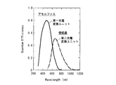
- the pin type first photoelectric conversion unit made of an amorphous silicon thin film and the pin type second photoelectric conversion unit made of a crystalline silicon thin film have the wavelength and The relationship with power generation efficiency is shown in FIG. As shown in FIG. 8, the pin-type second photoelectric conversion unit made of a crystalline silicon-based thin film has low power generation efficiency in the long wavelength region, and it is difficult to improve the photoelectric conversion efficiency of the entire device. It was.
- the present invention has been made in view of the above circumstances, and in a tandem photoelectric conversion device, the power generation efficiency in the long wavelength region of a pin-type second photoelectric conversion unit made of a crystalline silicon-based thin film is improved.
- a first object is to provide a tandem photoelectric conversion device with improved efficiency.
- a second object of the present invention is to provide a method for manufacturing a photoelectric conversion device capable of manufacturing a photoelectric conversion device having a tandem structure with improved photoelectric conversion efficiency by a simple method.
- the present invention also relates to a photoelectric conversion device having a single structure including a pin-type photoelectric conversion unit made of a crystalline silicon-based thin film, improving power generation efficiency in a long wavelength region and improving photoelectric conversion efficiency.
- a third object is to provide a device. Furthermore, this invention makes it the 4th objective to provide the manufacturing method of the photoelectric conversion apparatus which can manufacture the photoelectric conversion apparatus of the single structure which improved the photoelectric conversion efficiency by a simple method.
- the photoelectric conversion device includes: a substrate on which a transparent conductive film is formed; a first p-type semiconductor layer made of an amorphous silicon-based thin film on the transparent conductive film; A pin-type first photoelectric conversion unit formed by sequentially stacking a substantially intrinsic i-type semiconductor layer and a first n-type semiconductor layer; and a crystalline material on the first photoelectric conversion unit; A second p-type semiconductor layer made of a silicon-based thin film, a second substantially intrinsic i-type semiconductor layer, and a second n-type semiconductor layer made of an amorphous silicon-based thin film were sequentially stacked. a pin-type second photoelectric conversion unit; and a back electrode formed on the second photoelectric conversion unit.
- the thickness of the second n-type semiconductor layer is preferably 20 to 400 mm.
- the manufacturing method of the photoelectric conversion device according to the second aspect of the present invention is the first p, which is composed of an amorphous silicon thin film on the transparent conductive film formed on the substrate and constitutes the pin type first photoelectric conversion unit.
- a photoelectric conversion device includes: a substrate on which a transparent conductive film is formed; a third p-type semiconductor layer made of a crystalline silicon-based thin film on the transparent conductive film; A pin-type third photoelectric conversion unit formed by sequentially laminating an intrinsic i-type semiconductor layer and a third n-type semiconductor layer made of an amorphous silicon-based thin film; A back electrode formed thereon.
- the thickness of the third n-type semiconductor layer is preferably 20 to 400 mm.
- a method for producing a photoelectric conversion device comprising: a third photoelectric conversion unit comprising a crystalline silicon-based thin film on a transparent conductive film formed on a substrate; a p-type semiconductor layer and a third substantially intrinsic i-type semiconductor layer are sequentially formed; and the third photoelectric conversion unit is formed of an amorphous silicon-based thin film on the third i-type semiconductor layer. Forming a third n-type semiconductor layer; forming a back electrode on the third n-type semiconductor layer;
- the p layer and the i layer constituting the second photoelectric conversion unit are made of a crystalline silicon-based thin film, and the second photoelectric conversion unit is constituted.
- the n layer, which is disposed between the i layer and the back electrode and constitutes the second photoelectric conversion unit, is made of an amorphous silicon thin film.
- the function of the i layer made of a crystalline silicon-based thin film can be effectively utilized in the first photoelectric conversion unit, and lattice matching at the interface between the i layer and the back electrode can be obtained, and the second photoelectric conversion unit can be used.
- the open circuit voltage (Voc) on the conversion unit side can be improved.
- the power generation efficiency of a 2nd photoelectric conversion unit can be improved, and the photoelectric conversion efficiency as the whole apparatus can be improved.
- method for manufacturing device A a step of sequentially forming a p layer, an i layer, and an n layer of the first photoelectric conversion unit, A step of forming a p layer and an i layer constituting the second photoelectric conversion unit on the n layer of the conversion unit in order, and an n constituting the second photoelectric conversion unit on the i layer of the second photoelectric conversion unit A step of forming a layer, and a step of forming the back electrode on the n layer constituting the second photoelectric conversion unit, at least in order, so that the obtained photoelectric conversion device is provided on the second photoelectric conversion unit side.
- the open circuit voltage (Voc) can be improved. For this reason, the power generation efficiency of a 2nd photoelectric conversion unit can be improved, and the photoelectric conversion efficiency as the whole apparatus can be improved. As a result, according to the present invention, it is possible to provide a method of manufacturing a photoelectric conversion device that can easily manufacture a tandem photoelectric conversion device with improved photoelectric conversion efficiency.
- the p layer and i layer constituting the third photoelectric conversion unit are made of a crystalline silicon-based thin film, and the third photoelectric conversion unit
- the n layer constituting the third photoelectric conversion unit is made of an amorphous silicon-based thin film.
- the present invention it is possible to provide a photoelectric conversion device having a single structure with improved photoelectric conversion efficiency.
- the step of sequentially forming the p layer and the i layer of the third photoelectric conversion unit, a step of forming an n layer, and a step of forming the back electrode on the n layer constituting the third photoelectric conversion unit improves.
- an open circuit voltage (Voc) improves.
- Sectional drawing which shows an example of the laminated constitution of the photoelectric conversion apparatus (apparatus A) which concerns on this invention.
- Explanatory drawing which shows the process example of the manufacturing method of the photoelectric conversion apparatus shown in FIG.
- Explanatory drawing which shows the process example of the manufacturing method of the photoelectric conversion apparatus shown in FIG.
- Explanatory drawing which shows the process example of the manufacturing method of the photoelectric conversion apparatus shown in FIG.
- Schematic which shows an example of the manufacturing system which manufactures the photoelectric conversion apparatus which concerns on this invention.
- Sectional drawing which shows an example of the laminated constitution of the photoelectric conversion apparatus (apparatus B) which concerns on this invention.
- FIG. 1 is a cross-sectional view illustrating the layer structure of the photoelectric conversion device of the present invention.
- a p-type semiconductor layer (p layer), a substantially intrinsic i-type semiconductor layer (i layer), and n are formed on the first surface 1a of the substrate with a transparent conductive film.
- a pin-type first photoelectric conversion unit 3 and a second photoelectric conversion unit 4 each having a stacked type semiconductor layer (n layer) are sequentially stacked on the transparent conductive film 2. Further, a back electrode 5 is formed on the second photoelectric conversion unit 4 so as to overlap.
- the substrate 1 is made of an insulating material that is excellent in sunlight transmittance and durable, such as glass and transparent resin.
- the substrate 1 includes a transparent conductive film 2.
- the transparent conductive film 2 include light-transmitting metal oxides such as ITO (indium tin oxide), SnO 2 , and ZnO.
- the transparent conductive film 2 is formed on the substrate 1 by vacuum deposition or sputtering.
- this photoelectric conversion device 10 ⁇ / b> A (10) sunlight S is incident on the second surface 1 b of the substrate 1 as indicated by a white arrow in FIG. 1.
- the first photoelectric conversion unit 3 includes a p-type semiconductor layer (p layer, first p-type semiconductor layer) 31 and a substantially intrinsic i-type semiconductor layer (i layer, first i-type semiconductor layer) 32. , An n-type semiconductor layer (n layer, first n-type semiconductor layer) 33 is stacked. That is, the first photoelectric conversion unit 3 is formed by stacking the p layer 31, the i layer 32, and the n layer 33 in this order.
- the first photoelectric conversion unit 3 is made of an amorphous silicon material.
- the thickness of the p layer 31 is, for example, 80 mm
- the thickness of the i layer 32 is, for example, 1800 mm
- the thickness of the n layer 33 is, for example, 100 mm.
- the plasma CVD reaction chambers for forming the p layer 31, i layer 32, and n layer 43 of the first photoelectric conversion unit 3 are different from each other.
- the second photoelectric conversion unit 4 includes a p-type semiconductor layer (p layer, second p-type semiconductor layer) 41, a substantially intrinsic i-type semiconductor layer (i layer, second i-type semiconductor layer) 42, n And a pin structure in which a p-type semiconductor layer (n-layer, second n-type semiconductor layer) 43 is stacked. That is, the second photoelectric conversion unit 4 is formed by laminating the p layer 41, the i layer 42, and the n layer 43 in this order.
- the p-type semiconductor layer (p layer) 41 and the i-type semiconductor layer (i layer) 42 constituting the second photoelectric conversion unit 4 are made of a crystalline silicon-based thin film.
- the n-type semiconductor layer (n layer) 43 constituting the second photoelectric conversion unit 4 is amorphous by being formed between the i layer 42 constituting the second photoelectric conversion unit 4 and the back electrode 5.
- the silicon-based thin film is used.
- n layer 43 constituting the second photoelectric conversion unit 4 disposed between the i layer constituting the second photoelectric conversion unit 4 and the back electrode By forming the n layer 43 constituting the second photoelectric conversion unit 4 disposed between the i layer constituting the second photoelectric conversion unit 4 and the back electrode by an amorphous silicon-based thin film, The mismatch at the interface between the i layer 42 made of a crystalline silicon-based thin film and the back electrode 5 can be alleviated. Thereby, in the second photoelectric conversion unit 4, the function of the i layer 42 made of a crystalline silicon thin film can be effectively utilized, and lattice matching at the interface between the i layer 42 and the back electrode 5 can be obtained. The open circuit voltage (Voc) on the second photoelectric conversion unit 4 side can be improved.
- Voc open circuit voltage
- the power generation efficiency of the 2nd photoelectric conversion unit 4 can be improved, and the photoelectric conversion efficiency as the whole apparatus can be improved.
- the present invention it is possible to provide a tandem photoelectric conversion device with improved photoelectric conversion efficiency.
- the n-layer 43 made of an amorphous silicon-based thin film is similar to the amorphous n-layer 43 observed with a laser Raman microscope.
- the intensity (ic) of Raman scattered light caused by the crystalline silicon-based thin film is a peak near 520 nm. Is not observed.
- the n layer 43 has a conductivity of, for example, 1.0 ⁇ 10 ⁇ 4 to 1.0 ⁇ 10 ⁇ 2 S / cm.
- the thickness of the p-type semiconductor layer (p layer) 41 is 150 mm, for example, and the thickness of the i-type semiconductor layer (i layer) 42 is 15000 mm, for example.
- the thickness of the n-type semiconductor layer (n layer) 43 is preferably in the range of 20 to 400 mm, for example, and can be 50 mm, for example.
- the fill factor (FF) and the open circuit voltage (Voc) increase, and the effect of increasing the photoelectric conversion efficiency is recognized.
- the thickness of the n layer 43 is 400 mm or more, Jsc and Voc are lowered. This is presumably because the n-layer 43 absorbed light and the Jsc on the i-layer 42 side made of a crystalline silicon-based thin film was lowered.
- the back electrode 5 should just be comprised by electroconductive light reflection films, such as Ag (silver) and Al (aluminum).
- the back electrode 5 can be formed, for example, by sputtering or vapor deposition.
- a layer made of a conductive oxide such as ITO, SnO 2 , or ZnO is formed between the n-type semiconductor layer (n layer) 43 of the second photoelectric conversion unit 4 and the back electrode 5.
- a laminated structure may be employed.
- the manufacturing method of the photoelectric conversion device of the present invention includes a step of sequentially forming the p layer 31, the i layer 32, and the n layer 33 of the first photoelectric conversion unit 3, on the n layer 33 of the first photoelectric conversion unit 3, A step of sequentially forming a p layer 41 and an i layer 42 constituting the second photoelectric conversion unit 4, and an n layer 43 constituting the second photoelectric conversion unit 4 on the i layer 42 of the second photoelectric conversion unit 4. And the step of forming the back electrode 5 on the n layer 43 constituting the second photoelectric conversion unit 4 at least in order.
- the open circuit voltage (Voc) on the unit 4 side can be improved.
- the power generation efficiency of the 2nd photoelectric conversion unit 4 can be improved, and the photoelectric conversion efficiency as the whole apparatus can be improved.
- the present invention it is possible to easily manufacture a tandem photoelectric conversion device with improved photoelectric conversion efficiency.
- it demonstrates in order of a process.
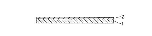
- an insulating transparent substrate 1 on which a transparent conductive film 2 is formed is prepared.
- the p-type semiconductor layer 31 and the i-type silicon layer (amorphous silicon layer) of the first photoelectric conversion unit 3 are formed on the transparent conductive film 2 formed on the insulating transparent substrate 1.
- Layer) 32, the n-type semiconductor layer 33, and the p-type semiconductor layer 41 of the second photoelectric conversion unit 4 are formed.
- the plasma CVD reaction chambers for forming the p layer 31, the i layer 32, the n layer 33, and the p layer 41 are different. That is, on the n-type semiconductor layer 33 of the first photoelectric conversion unit 3, the photoelectric conversion device first intermediate product 10a provided with the p-type semiconductor layer 41 constituting the second photoelectric conversion unit 4 is formed.
- the p-type semiconductor layer 31 is formed by plasma CVD in an individual reaction chamber.
- the substrate temperature is 180 to 200 ° C.
- the power supply frequency is 13.56 MHz
- the reaction chamber pressure is 70 to 120 Pa
- the reaction gas flow rate is 300 sccm for monosilane (SiH 4 ), 2300 sccm for hydrogen (H 2 ), and hydrogen as a dilution gas
- the p-layer 31 of amorphous silicon (a-Si) can be formed under the conditions of 180 sccm for diborane (B 2 H 6 / H 2 ) and 500 sccm for methane (CH 4 ).
- the i-type silicon layer (amorphous silicon layer) 32 is formed by plasma CVD in a separate reaction chamber.
- the substrate temperature is 180 to 200 ° C.
- the power supply frequency is 13.56 MHz
- the pressure in the reaction chamber is 70 to 120 Pa
- the reaction gas flow rate is 1200 scc for monosilane (SiH 4 )
- the amorphous silicon (a-Si) i Layer 32 can be deposited.
- the n-type semiconductor layer 33 is formed by plasma CVD in a separate reaction chamber.
- the substrate temperature is 180 to 200 ° C.
- the power supply frequency is 13.56 MHz
- the pressure in the reaction chamber is 70 to 120 Pa
- the flow rate of the reaction gas is phosphine (PH 3 / H 2 ) using hydrogen as a diluent gas at 200 sccm.
- a-Si amorphous silicon
- the p-type semiconductor layer 41 is formed by plasma CVD in a separate reaction chamber.
- the substrate temperature is 180 to 200 ° C.
- the power supply frequency is 13.56 MHz
- the reaction chamber pressure is 500 to 900 Pa
- the reaction gas flow rate is 100 sccm for monosilane (SiH 4 ), 25000 sccm for hydrogen (H 2 ), and hydrogen as a dilution gas
- the p-layer 41 of microcrystalline silicon ( ⁇ c-Si) can be formed under the condition that the diborane (B 2 H 6 / H 2 ) used as is 50 sccm.
- the second photoelectric conversion unit 4 is formed on the p-type semiconductor layer 41 exposed to the atmosphere.
- An i-type silicon layer (crystalline silicon layer) 42 and an n-type semiconductor layer (amorphous silicon layer) 43 are formed in the same plasma CVD reaction chamber. That is, the second intermediate product 10 b of the photoelectric conversion device in which the second photoelectric conversion unit 4 is provided is formed on the first photoelectric conversion unit 3.
- the i-type silicon layer (crystalline silicon layer) 42 is formed by a plasma CVD method in the same reaction chamber as the reaction chamber in which the n-type semiconductor layer 43 is formed.
- the substrate temperature is 180 to 200 ° C.
- the power supply frequency is 13.56 MHz
- the pressure in the reaction chamber is 500 to 900 Pa
- the reaction gas flow rate is 180 sccm for monosilane (SiH 4 ) and 27000 sccm for hydrogen (H 2 )
- An i-layer of microcrystalline silicon ( ⁇ c-Si) can be formed.
- the n-type semiconductor layer 43 is formed by plasma CVD in the same reaction chamber as the reaction chamber in which the i-type silicon layer (crystalline silicon layer) 42 is formed.
- the substrate temperature is 180 to 200 ° C.
- the power supply frequency is 13.56 MHz
- the pressure in the reaction chamber is 70 to 120 Pa
- the flow rate of the reaction gas is phosphine (PH 3 / H 2 ) using hydrogen as a diluent gas at 200 sccm.
- a-Si amorphous silicon
- the photoelectric conversion apparatus 10A (10) as shown in FIG. 1 is obtained by forming the back surface electrode 5 on the n-type semiconductor layer 43 of the second photoelectric conversion unit 4.
- the back electrode 5 should just be comprised by electroconductive light reflection films, such as Ag (silver) or Al (aluminum).
- the back electrode 5 can be formed, for example, by sputtering or vapor deposition.
- the manufacturing system of the photoelectric conversion device 10 includes a so-called in-line type first film forming device, an exposure device that exposes the p-layer of the second photoelectric conversion unit 4 to the atmosphere, and a so-called batch type second component.
- the membrane device is arranged in order.
- the in-line type first film forming apparatus has a configuration in which a plurality of film forming reaction chambers called chambers are arranged in a straight line.
- the p-type semiconductor layer 31, the i-type silicon layer (amorphous silicon layer) 32, the n-type semiconductor layer 33, and the second photoelectric conversion unit 4 in the first photoelectric conversion unit 3 are used.
- Each layer of the type semiconductor layer 41 is formed separately.
- each of the i-type silicon layer (crystalline silicon layer) 42 and the n-type semiconductor layer (amorphous silicon layer) 43 in the second photoelectric conversion unit 4 is simultaneously applied to a plurality of substrates. Are formed in the same film formation reaction chamber.
- a manufacturing system of the photoelectric conversion device 10 is shown in FIG. As shown in FIG. 3, the manufacturing system exposes the first film forming apparatus 60, the second film forming apparatus 70, and the substrate processed by the first film forming apparatus 60 to the second film forming apparatus 70. And a moving exposure device 80.
- the first film forming apparatus 60 in the manufacturing system is provided with a load chamber (L: Load) 61 in which the substrate is first carried and the internal pressure is reduced. Note that a heating chamber for heating the substrate temperature to a certain temperature may be provided in the subsequent stage of the load chamber (L: Load) 61 in accordance with the film forming process.
- An n-layer film formation reaction chamber 64 for forming the layer 33 and a p-layer film formation reaction chamber 65 for forming the p-type semiconductor layer 41 of the second photoelectric conversion unit 4 are continuously arranged in a straight line.
- an unload chamber (UL: UnLoad, unloading device) 66 for returning the reduced-pressure atmosphere to the atmospheric atmosphere and unloading the substrate is connected to the p-layer film formation reaction chamber 65.
- an insulating transparent substrate 1 on which the transparent conductive film 2 is formed is prepared.
- the p-type semiconductor layer 31 of the first photoelectric conversion unit 3 is formed on the transparent conductive film 2 formed on the insulating transparent substrate 1, as shown in FIG. 2B.
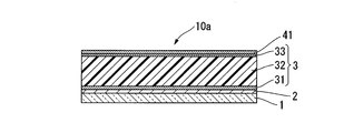
- the first intermediate product 10a of the photoelectric conversion device provided with the i-type silicon layer (amorphous silicon layer) 32, the n-type semiconductor layer 33, and the p-type semiconductor layer 41 of the second photoelectric conversion unit 4 is formed.
- the second film forming apparatus 70 in the manufacturing system includes a load / unload chamber (L / UL) 71 and an in-layer film forming reaction chamber 72.
- the load / unload chamber (L / UL) 71 carries in the first intermediate product 10a of the photoelectric conversion device processed by the first film forming device 60, and reduces the internal pressure after the substrate is carried in, The reduced-pressure atmosphere is returned to the air atmosphere when unloading.
- the in-layer deposition reaction chamber 72 is connected to the load / unload chamber (L / UL) 71.
- the i-type silicon layer (crystalline silicon layer) 42 and the n-type semiconductor layer (non-layer) of the second photoelectric conversion unit 4 are formed on the p-type semiconductor layer 41 of the second photoelectric conversion unit 4.
- a crystalline silicon layer) 43 is sequentially formed in the same reaction chamber. Further, this film forming process is performed simultaneously on a plurality of substrates. At this time, the second intermediate product 10b of the photoelectric conversion device in which the second photoelectric conversion unit 4 is provided is formed on the first photoelectric conversion unit 3, as shown in FIG. .
- the i-layer film forming reaction chamber 63 includes four reaction chambers 63a and 63b. , 63c, 63d.
- the batch-type second film forming apparatus 70 is configured to process six substrates simultaneously.
- the photoelectric conversion device is a crystalline photoelectric conversion device on the p layer 31, the i layer 32, and the n layer 33 of the first photoelectric conversion unit 3 that is an amorphous photoelectric conversion device.
- the p layer 41 of the second photoelectric conversion unit 4 is formed.
- the i layer 42 and the n layer 43 of the second photoelectric conversion unit 4 are formed. Thereby, it is possible to easily control the crystallization rate distribution of the i layer 42 of the second photoelectric conversion unit 4.
- the i-type silicon layer (crystalline silicon layer) 42 and the n-type semiconductor layer 43 constituting the second photoelectric conversion unit 4 are formed on the p-type semiconductor layer 41 exposed in the atmosphere.
- the p layer, i layer, and n of the first photoelectric conversion unit 3 are formed on the transparent metal oxide electrode of the glass substrate 1 with the transparent metal oxide electrode (transparent conductive film 2) in a separate film formation chamber.
- the OH radical-containing plasma processing chamber is used. Thereafter, the i-type silicon layer (crystalline silicon layer) 42 and the n-type semiconductor layer 43 constituting the second photoelectric conversion unit 4 may be formed in separate film formation chambers or in the same processing chamber. The i layer 42 and the n layer 43 of the second photoelectric conversion unit 4 may be laminated continuously with the radical-containing plasma treatment.
- the film formation chamber is treated with the OH radical-containing plasma for each treatment. Apply. This enables decomposition and removal of the residual impurity gas PH 3. Therefore, even if the film formation of the i layer 42 and the n layer 43 of the second photoelectric conversion unit 4 is repeated in the same processing chamber, a good impurity profile can be obtained, and the laminated thin film photoelectric conversion device 10 with good power generation efficiency can be obtained. Can do.
- CO 2 , CH 2 O 2 or a mixture of H 2 O and H 2 is used as a process gas. It is desirable to use gas. That is, for the generation of OH radical-containing plasma, (CO 2 + H 2 ), (CH 2 O 2 + H 2 ), or (H 2 O + H 2 ) is allowed to flow in the film formation chamber between the electrodes, for example, 13. It can be effectively generated by applying a high frequency such as 5 MHz, 27 MHz, or 40 MHz.
- alcohols such as (HCOOCH 2 + H 2 ) and (CH 2 OH + H 2 ), and oxygen-containing hydrocarbons such as formate esters may be used.
- oxygen-containing hydrocarbons such as formate esters
- H 2 When CO 2 is used as the plasma generation gas in the generation of this OH radical-containing plasma, the presence of H 2 is necessary in the system, but in addition to (CH 2 O 2 + H 2 ) and (H 2 O + H 2 ), When oxygen-containing hydrocarbons such as alcohols such as (HCOOCH 3 + H 2 ) and (CH 3 OH + H 2 ) and formate esters are used, the presence of H 2 is not necessarily required in the system.
- the reaction is milder than that of the O radical and the lower layer is not damaged, and the p layer 31, i layer 32, and n layer 33 of the first photoelectric conversion unit 3 are not damaged.
- This is effective for the surface activity of the p layer 41 of the formed second photoelectric conversion unit 4. Therefore, the surface activation of the p layer 41 of the second photoelectric conversion unit 4 becomes possible. It effectively works for crystal formation of the i layer 42 of the second photoelectric conversion unit 4 laminated thereon, and a uniform crystallization rate distribution can be obtained even on a large-area substrate. Even if the hydrogen plasma treatment is performed instead of the OH radical-containing plasma treatment, the same effect as the OH radical-containing plasma treatment can be obtained.
- the p layer 41 of the second photoelectric conversion unit 4 formed on the amorphous p layer 31, i layer 32, and n layer 33 of the first photoelectric conversion unit 3 in an individual film formation chamber is amorphous.
- amorphous amorphous oxidation is required. It is preferable to employ a film in which microcrystalline silicon ( ⁇ c-Si) is dispersed in the silicon (a-SiO) layer.
- a film in which microcrystalline silicon ( ⁇ c-Si) is dispersed in an amorphous amorphous silicon oxide (a-SiO) layer has a lower refractive index than an amorphous silicon (a-Si) semiconductor layer. It is possible to adjust as follows. Therefore, it is possible to improve the conversion efficiency by making this layer function as a wavelength selective reflection film and confining short wavelength light on the top cell side. Regardless of the effect of confining light, a film in which microcrystalline silicon ( ⁇ c-Si) is dispersed in an amorphous amorphous silicon oxide (a-SiO) layer is subjected to OH radical-containing plasma treatment. It is effective for generating crystal growth nuclei of the i-layer 42 and the n-layer 43 of the two photoelectric conversion unit 4, and a uniform crystallization rate distribution can be obtained even on a large-area substrate.
- a crystalline silicon-based thin film may be formed as the n layer 33 constituting the first photoelectric conversion unit 3. That is, the crystalline n layer 33 and the p layer 41 of the crystalline second photoelectric conversion unit 4 are formed on the p layer 31 and the i layer 32 of the amorphous first photoelectric conversion unit 3.
- the substrate on which the n layer 33 and the p layer 41 of the second photoelectric conversion unit 4 are formed is subjected to OH radical-containing plasma treatment in an individual reaction chamber or the same film formation chamber, and the surface is activated to produce crystals.
- a laminated thin film photoelectric conversion device 10A (10 having a uniform crystallization rate distribution over a large area and good power generation efficiency. ) Can be obtained.
- FIG. 4 is a cross-sectional view illustrating a layer configuration of the photoelectric conversion device according to the present embodiment.
- the tandem structure photoelectric conversion device has been described.
- the present invention is not limited to the tandem structure, and can be applied to a single structure photoelectric conversion device.
- this photoelectric conversion device 10B a substrate with a transparent conductive film is used, a p-type semiconductor layer (p layer, third p-type semiconductor layer) 81, a substantially intrinsic i-type semiconductor layer (i layer, A pin type third photoelectric conversion unit 8 in which a third i-type semiconductor layer) 82 and an n-type semiconductor layer (n-layer, third n-type semiconductor layer) 83 are stacked, and the back electrode 5 include the transparent conductive material.
- the film 2 is formed on the film 2 in order.
- the p layer 81 and the i layer 82 constituting the third photoelectric conversion unit 8 are formed of a crystalline silicon-based thin film, and the third photoelectric conversion unit 8 is configured.
- the n layer 83 disposed between the i layer 82 and the back electrode 5 and constituting the third photoelectric conversion unit 8 is formed of an amorphous silicon-based thin film.
- the p layer 81 and i layer 82 constituting the third photoelectric conversion unit 8 are formed of a crystalline silicon thin film, and the i layer 82 constituting the third photoelectric conversion unit 8.
- an n-layer 83 disposed between the back electrode 5 and the third photoelectric conversion unit 8 is formed of an amorphous silicon-based thin film, thereby forming an i-layer 82 formed of a crystalline silicon-based thin film,
- the mismatch at the interface of the back electrode 5 can be alleviated.
- the function of the i layer 82 formed of a crystalline silicon-based thin film can be effectively utilized, and the open circuit voltage (Voc) is improved.
- the photoelectric conversion efficiency of the photoelectric conversion device 10B (10) is improved.
- the manufacturing method of the photoelectric conversion apparatus 10B (10) of this invention forms the p layer 81 and the i layer 82 of the 3rd photoelectric conversion unit 8 in order, and forms the n layer 83 of the 3rd photoelectric conversion unit 8.
- the p layer 81, i layer 82, and n layer 83 constituting the third photoelectric conversion unit 8 are all the p layer 41, i layer 42, and the second photoelectric conversion unit 4 in the first embodiment described above.
- the n layer 43 can be formed in the same manner.
- the open circuit voltage (Voc) is improved, and the photoelectric conversion efficiency is improved.
- the manufacturing method of the present invention it is possible to easily manufacture the photoelectric conversion device 10B (10) with improved photoelectric conversion efficiency.
- the photoelectric conversion device is manufactured using a substrate having a size of 1100 mm ⁇ 1400 mm.
- the first photoelectric conversion unit is formed of a p-layer made of an amorphous amorphous silicon (a-Si) thin film, a buffer layer, and an amorphous amorphous silicon (a-Si) thin film on the substrate.
- a-Si amorphous amorphous silicon
- a buffer layer a buffer layer
- a-Si amorphous amorphous silicon
- An i layer, an n layer composed of an amorphous silicon (a-Si) thin film, and a p layer containing microcrystalline silicon ( ⁇ c-Si) constituting the second photoelectric conversion unit were formed. These layers are successively formed in separate film formation chambers.
- the p layer of the second photoelectric conversion unit was exposed to the atmosphere, and hydrogen plasma treatment was performed on the p layer of the second photoelectric conversion unit using hydrogen (H 2 ) as a process gas. Thereafter, an i layer made of microcrystalline silicon ( ⁇ c-Si), an n layer made of an amorphous silicon (a-Si) thin film, and a back electrode constituting the second photoelectric conversion unit were formed.
- ⁇ c-Si microcrystalline silicon
- a-Si amorphous silicon
- Example 1 the p layer, i layer, and n layer of the first photoelectric conversion unit and the p layer of the second photoelectric conversion unit were formed by plasma CVD in individual reaction chambers. On the other hand, the i layer and the n layer of the second photoelectric conversion unit were formed by plasma CVD in the same film formation chamber.
- the p layer of the first photoelectric conversion unit has a substrate temperature of 170 ° C., an applied RF power of 40 W, a reaction chamber pressure of 80 Pa, and a reaction gas flow rate of 150 cc for monosilane (SiH 4 ), 470 sccm for hydrogen (H 2 ), hydrogen As a diluent gas, a film was formed to a thickness of 80 mm under conditions of 45 sccm for diborane (B 2 H 6 / H 2 ) and 300 sccm for methane (CH 4 ). The deposition rate at this time was 116 ⁇ / min.
- the buffer layer has a substrate temperature of 170 ° C., an applied RF power of 40 W, a reaction chamber pressure of 60 Pa, a reaction gas flow rate of 150 sccm for monosilane (SiH 4 ), 1500 sccm for hydrogen (H 2 ), and methane (CH 4 ).
- SiH 4 monosilane
- SiH 2 1500 sccm for hydrogen
- CH 4 methane
- the i layer of the first photoelectric conversion unit has a substrate temperature of 170 ° C., an applied RF power of 40 W, a reaction chamber pressure of 40 Pa, and a reaction gas flow rate of 2000 ⁇ with monosilane (SiH 4 ) of 300 sccm. A film was formed. The film formation rate at this time was 131 kg / min. Furthermore, the n layer of the first photoelectric conversion unit has a substrate temperature of 170 ° C., an applied RF power of 1000 W, a reaction chamber pressure of 800 Pa, and a reaction gas flow rate of 150 cc for monosilane (SiH 4 ) and 550 sccm for hydrogen (H 2 ).
- the film was formed to a thickness of 20 mm under the condition of 60 sccm of phosphine (PH 3 / H 2 ) using hydrogen as a diluent gas. At this time, the deposition rate was 158 ⁇ / min.
- the substrate temperature is 170 ° C.
- the applied RF power is 750 W
- the reaction chamber pressure is 1200 Pa
- the reaction gas flow rate is 30 sccm for monosilane (SiH 4 )
- the reaction gas flow rate is 30 sccm for monosilane (SiH 4 )
- the film was formed to a thickness of 150 mm under conditions of 9000 sccm and diborane (B 2 H 6 / H 2 ) using hydrogen as a diluent gas at 12 sccm.
- the film formation rate at this time was 174 ⁇ / min.
- the p layer of the second photoelectric conversion unit was exposed to the atmosphere.
- the p layer was subjected to plasma treatment under the conditions of a substrate temperature of 190 ° C., a power supply frequency of 13.56 MHz, a reaction chamber pressure of 700 Pa, and H 2 as a process gas of 1000 sccm.
- the i layer of the second photoelectric conversion unit has a substrate temperature of 170 ° C., an applied RF power of 550 W, a reaction chamber pressure of 1200 Pa, and a reaction gas flow rate of 45 sccm for monosilane (SiH 4 ) and 3150 sccm for hydrogen (H 2 ).
- a film having a thickness of 15000 mm was formed. At this time, the film formation rate was 361 L / min.
- the n layer of the second photoelectric conversion unit has a substrate temperature of 170 ° C., an applied RF power of 100 W, a reaction chamber pressure of 80 Pa, and a reaction gas flow rate of 150 sccm for monosilane (SiH 4 ) and 550 sccm for hydrogen (H 2 ).
- the film was formed to a thickness of 20 mm under the condition of 60 sccm of phosphine (PH 3 / H 2 ) using hydrogen as a diluent gas. At this time, the deposition rate was 158 ⁇ / min.
- zinc oxide (ZnO) was formed to a thickness of 800 mm on the n layer of the second photoelectric conversion unit by sputtering. Further, silver (Ag) was formed thereon to a film thickness of 2000 mm to form a back electrode.
- Example 2 to Example 6 The thickness of the n layer constituting the second photoelectric conversion unit is changed to 20 mm, 50 mm (Example 2), 100 mm (Example 3), 150 mm (Example 4), 200 mm (Example 5), 400 mm (implemented)
- a tandem photoelectric conversion device was produced in the same manner as in Example 1 except that Example 6) was used.
- n layer constituting the second photoelectric conversion unit was an n layer made of microcrystalline silicon ( ⁇ c-Si).
- the n layer of the second photoelectric conversion unit has a substrate temperature of 170 ° C., an applied RF power of 1000 W, a reaction chamber pressure of 800 Pa, a reaction gas flow rate of 20 sccm for monosilane (SiH 4 ), 2000 sccm for hydrogen (H 2 ), hydrogen was used to form a film having a thickness of 100 mm under the condition of 15 sccm of phosphine (PH 3 / H 2 ) using as a diluent gas.
- the film formation rate at this time was 174 ⁇ / min.
- the conventional photoelectric conversion device (comparative example) Compared to the above, it showed good characteristics, and in particular, the photoelectric conversion efficiency could be improved by about 0.5% (contrast of Example 3 and Comparative Example).
- FIGS. 5 and 6 show the photoelectric conversion efficiency ( ⁇ ) and the open-circuit voltage (Voc) obtained when the thickness of the n layer of the second photoelectric conversion unit was changed for the photoelectric conversion devices of Examples 1 to 6. ) Shows the measurement results. That is, FIGS. 5 and 6 are graphs in which ⁇ and Voc (vertical axis) are plotted with respect to the thickness (horizontal axis) of the n layer. As shown in Table 1, FIG. 5, and FIG. 6, when the thickness (film thickness) of the n layer is in the range of 20 to 400 mm, the open circuit voltage (Voc) increases and the photoelectric conversion efficiency ⁇ increases. It is done.
- the film thickness of the n layer constituting the second light conversion unit is preferably in the range of 20 to 400 mm, and more preferably in the range of 100 to 200 mm.
- the present invention is widely applicable to photoelectric conversion devices and methods for manufacturing photoelectric conversion devices.
- first photoelectric conversion unit second photoelectric conversion unit 5 back electrode 10A, 10B (10) photoelectric conversion device 31 p-type semiconductor layer (first p-type semiconductor layer) 32 i-type silicon layer (amorphous silicon layer, first i-type semiconductor layer) 33 n-type semiconductor layer (first n-type semiconductor layer) 41 p-type semiconductor layer (second p-type semiconductor layer) 42 i-type silicon layer (crystalline silicon layer, second i-type semiconductor layer) 43 n-type semiconductor layer (second n-type semiconductor layer) 8 First photoelectric conversion unit 81 p-type semiconductor layer (third p-type semiconductor layer) 82 i-type silicon layer (crystalline silicon layer, third i-type semiconductor layer) 83 n-type semiconductor layer (third n-type semiconductor layer) 60 First film formation apparatus 61 Load chamber 62 P layer film formation reaction chamber 63 (63a, 63b, 63c, 63d) i layer film formation reaction chamber 64 n
Landscapes
- Photovoltaic Devices (AREA)
Abstract
この光電変換装置は、透明導電膜が形成された基板と;前記透明導電膜の上に、アモルファスのシリコン系薄膜からなる、第1のp型半導体層と、第1の実質的に真性なi型半導体層と、第1のn型半導体層とを順に積層して形成されたpin型の第一光電変換ユニットと;前記第一光電変換ユニットの上に、結晶質のシリコン系薄膜からなる第2のp型半導体層と第2の実質的に真性なi型半導体層と、アモルファスのシリコン系薄膜からなる第2のn型半導体層とを順に積層して形成されたpin型の第二光電変換ユニットと;前記第二光電変換ユニットの上に形成された裏面電極と;を備える。
Description
本発明は、光電変換装置及び光電変換装置の製造方法に関する。
本願は、2010年4月2日に、日本に出願された特願2010-086181号に基づき優先権を主張し、その内容をここに援用する。
本願は、2010年4月2日に、日本に出願された特願2010-086181号に基づき優先権を主張し、その内容をここに援用する。
近年、光電変換装置は、太陽電池又は光センサなどに一般的に利用されており、とりわけ太陽電池においては、エネルギーの効率的な利用の観点から広く普及を始めている。特に、単結晶シリコンを利用した光電変換装置は、単位面積当たりのエネルギー変換効率に優れている。しかし、一方で単結晶シリコンを利用した光電変換装置は、単結晶シリコンインゴットをスライスしたシリコンウエハを用いるため、インゴットの製造に大量のエネルギーが費やされ、製造コストが高い。例えば、屋外などに設置される大面積の光電変換装置を、シリコン単結晶を利用して製造すると、現状では相当にコストが掛かる。そこで、より安価に製造可能なアモルファス(非晶質)シリコン薄膜(以下、「a-Si薄膜」とも表記する)を利用した光電変換装置が、ローコストな光電変換装置として普及している。
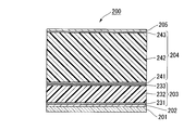
ところが、このアモルファス(非晶質)シリコン薄膜を利用した光電変換装置の変換効率は、単結晶シリコン又は多結晶シリコン等を利用した結晶型の光電変換装置の変換効率に比べて低い。そこで、光電変換装置の変換効率を向上させる構造として、2つの光電変換ユニットが積層されたタンデム型の構造が提案されている。たとえば、図7に示すようなタンデム型の光電変換装置200が知られている。このタンデム型の光電変換装置200においては、透明導電膜202が配された絶縁性の透明基板201が用いられている。透明導電膜202上には、p型半導体層231、i型シリコン層(非晶質シリコン層)232、n型半導体層233、を順次積層して得られたpin型の第一光電変換ユニット203が形成されている。第一光電変換ユニット203上には、p型半導体層241、i型シリコン層(結晶質シリコン層)242、n型半導体層243、を順次積層して得られたpin型の第二光電変換ユニット204が形成されている。さらに、第二光電変換ユニット204上には、裏面電極205が形成されている。このようなタンデム型の光電変換装置を製造する方法としては、例えば、特許文献1に開示された製造方法が知られている。
このようなタンデム構造の光電変換装置において、非晶質のシリコン系薄膜からなるpin型の第一光電変換ユニットと、結晶質のシリコン系薄膜からなるpin型の第二光電変換ユニットについて、波長と発電効率との関係を図8に示す。
図8に示されるように、結晶質のシリコン系薄膜からなるpin型の第二光電変換ユニットは、長波長領域における発電効率が低く、装置全体としての光電変換効率を向上させることが困難であった。
図8に示されるように、結晶質のシリコン系薄膜からなるpin型の第二光電変換ユニットは、長波長領域における発電効率が低く、装置全体としての光電変換効率を向上させることが困難であった。
本発明は上記事情に鑑みてなされたもので、タンデム構造の光電変換装置において、結晶質のシリコン系薄膜からなるpin型の第二光電変換ユニットにおける長波長領域の発電効率を改善し、光電変換効率を向上させたタンデム構造の光電変換装置を提供することを第一の目的とする。
また、本発明は、光電変換効率を向上させたタンデム構造の光電変換装置を簡便な方法で製造することが可能な光電変換装置の製造方法を提供することを第二の目的とする。
また、本発明は、結晶質のシリコン系薄膜からなるpin型の光電変換ユニットを備えたシングル構造の光電変換装置において、長波長領域の発電効率を改善し、光電変換効率を向上させた光電変換装置を提供することを第三の目的とする。
さらに、本発明は、光電変換効率を向上させたシングル構造の光電変換装置を簡便な方法で製造することが可能な光電変換装置の製造方法を提供することを第四の目的とする。
また、本発明は、光電変換効率を向上させたタンデム構造の光電変換装置を簡便な方法で製造することが可能な光電変換装置の製造方法を提供することを第二の目的とする。
また、本発明は、結晶質のシリコン系薄膜からなるpin型の光電変換ユニットを備えたシングル構造の光電変換装置において、長波長領域の発電効率を改善し、光電変換効率を向上させた光電変換装置を提供することを第三の目的とする。
さらに、本発明は、光電変換効率を向上させたシングル構造の光電変換装置を簡便な方法で製造することが可能な光電変換装置の製造方法を提供することを第四の目的とする。
本発明の第1態様の光電変換装置は、透明導電膜が形成された基板と;前記透明導電膜の上に、アモルファスのシリコン系薄膜からなる、第1のp型半導体層と、第1の実質的に真性なi型半導体層と、第1のn型半導体層とを順に積層して形成されたpin型の第一光電変換ユニットと;前記第一光電変換ユニットの上に、結晶質のシリコン系薄膜からなる第2のp型半導体層と第2の実質的に真性なi型半導体層と、アモルファスのシリコン系薄膜からなる第2のn型半導体層とを順に積層して形成されたpin型の第二光電変換ユニットと;前記第二光電変換ユニットの上に形成された裏面電極と;を備える。
本発明の第1態様の光電変換装置においては、前記第2のn型半導体層の厚みが、20~400Åであることが好ましい。
本発明の第2態様の光電変換装置の製造方法は、基板に形成された透明導電膜の上に、アモルファスのシリコン系薄膜からなりpin型の第一光電変換ユニットを構成する、第1のp型半導体層と、第1の実質的に真性なi型半導体層と、第1のn型半導体層とを順に形成し;前記第1のn型半導体層の上に、結晶質のシリコン系薄膜からなりpin型の第二光電変換ユニットを構成する、第2のp型半導体層と、第2の実質的に真性なi型半導体層とを順に形成し;前記第2のi型半導体層の上に、アモルファスのシリコン系薄膜からなり前記第二光電変換ユニットを構成する、第2のn型半導体層を形成し;前記第2のn型半導体層の上に、裏面電極を形成する。
本発明の第3態様の光電変換装置は、透明導電膜が形成された基板と;前記透明導電膜の上に、結晶質のシリコン系薄膜からなる第3のp型半導体層と第3の実質的に真性なi型半導体層と、アモルファスのシリコン系薄膜からなる第3のn型半導体層とを順に積層して形成されたpin型の第三光電変換ユニットと;前記第三光電変換ユニットの上に形成された裏面電極と;を備える。
本発明の第3態様の光電変換装置においては、前記第3のn型半導体層の厚みが、20~400Åであることが好ましい。
本発明の第4態様の光電変換装置の製造方法は、基板に形成された透明導電膜の上に、結晶質のシリコン系薄膜からなりpin型の第三光電変換ユニットを構成する、第3のp型半導体層と、第3の実質的に真性なi型半導体層とを順に形成し;前記第3のi型半導体層の上に、アモルファスのシリコン系薄膜からなり前記第三光電変換ユニットを構成する、第3のn型半導体層を形成し;前記第3のn型半導体層の上に、裏面電極を形成する。
本発明の第1態様の光電変換装置においては、前記第2のn型半導体層の厚みが、20~400Åであることが好ましい。
本発明の第2態様の光電変換装置の製造方法は、基板に形成された透明導電膜の上に、アモルファスのシリコン系薄膜からなりpin型の第一光電変換ユニットを構成する、第1のp型半導体層と、第1の実質的に真性なi型半導体層と、第1のn型半導体層とを順に形成し;前記第1のn型半導体層の上に、結晶質のシリコン系薄膜からなりpin型の第二光電変換ユニットを構成する、第2のp型半導体層と、第2の実質的に真性なi型半導体層とを順に形成し;前記第2のi型半導体層の上に、アモルファスのシリコン系薄膜からなり前記第二光電変換ユニットを構成する、第2のn型半導体層を形成し;前記第2のn型半導体層の上に、裏面電極を形成する。
本発明の第3態様の光電変換装置は、透明導電膜が形成された基板と;前記透明導電膜の上に、結晶質のシリコン系薄膜からなる第3のp型半導体層と第3の実質的に真性なi型半導体層と、アモルファスのシリコン系薄膜からなる第3のn型半導体層とを順に積層して形成されたpin型の第三光電変換ユニットと;前記第三光電変換ユニットの上に形成された裏面電極と;を備える。
本発明の第3態様の光電変換装置においては、前記第3のn型半導体層の厚みが、20~400Åであることが好ましい。
本発明の第4態様の光電変換装置の製造方法は、基板に形成された透明導電膜の上に、結晶質のシリコン系薄膜からなりpin型の第三光電変換ユニットを構成する、第3のp型半導体層と、第3の実質的に真性なi型半導体層とを順に形成し;前記第3のi型半導体層の上に、アモルファスのシリコン系薄膜からなり前記第三光電変換ユニットを構成する、第3のn型半導体層を形成し;前記第3のn型半導体層の上に、裏面電極を形成する。
本発明の光電変換装置(以下、「装置A」とも呼ぶ)では、前記第二光電変換ユニットを構成するp層、i層が結晶質のシリコン系薄膜からなり、前記第二光電変換ユニットを構成するi層と前記裏面電極との間に配され、前記第二光電変換ユニットを構成するn層がアモルファスのシリコン系薄膜からなる。これにより、結晶質のシリコン系薄膜からなるi層と、裏面電極との界面における不整合を緩和することができる。これにより、第一光電変換ユニットにおいて結晶質のシリコン系薄膜からなるi層の働きを有効に活用することができ、このi層と、裏面電極との界面の格子整合を得るとともに、第二光電変換ユニット側の開放電圧(Voc)を向上することができる。このため、第二光電変換ユニットの発電効率を向上させ、装置全体としての光電変換効率を向上させることができる。その結果、本発明によれば、光電変換効率が向上したタンデム構造の光電変換装置を提供することが可能である。
また、本発明の光電変換装置の製造方法(以下、「装置Aの製法」とも呼ぶ)では、前記第一光電変換ユニットのp層、i層、n層を順に形成するステップ、前記第一光電変換ユニットのn層上に、前記第二光電変換ユニットを構成するp層、i層を順に形成するステップ、前記第二光電変換ユニットのi層上に、前記第二光電変換ユニットを構成するn層を形成するステップ、前記第二光電変換ユニットを構成するn層上に、前記裏面電極を形成するステップ、を少なくとも順に備えているので、得られる光電変換装置は、第二光電変換ユニット側の開放電圧(Voc)を向上することができる。このため、第二光電変換ユニットの発電効率を向上させ、装置全体としての光電変換効率を向上させることができる。その結果、本発明によれば、光電変換効率が向上したタンデム構造の光電変換装置を簡便に製造できる光電変換装置の製造方法を提供することが可能である。
また、本発明の光電変換装置の製造方法(以下、「装置Aの製法」とも呼ぶ)では、前記第一光電変換ユニットのp層、i層、n層を順に形成するステップ、前記第一光電変換ユニットのn層上に、前記第二光電変換ユニットを構成するp層、i層を順に形成するステップ、前記第二光電変換ユニットのi層上に、前記第二光電変換ユニットを構成するn層を形成するステップ、前記第二光電変換ユニットを構成するn層上に、前記裏面電極を形成するステップ、を少なくとも順に備えているので、得られる光電変換装置は、第二光電変換ユニット側の開放電圧(Voc)を向上することができる。このため、第二光電変換ユニットの発電効率を向上させ、装置全体としての光電変換効率を向上させることができる。その結果、本発明によれば、光電変換効率が向上したタンデム構造の光電変換装置を簡便に製造できる光電変換装置の製造方法を提供することが可能である。
また、本発明の光電変換装置(以下、「装置B」とも呼ぶ)では、前記第三光電変換ユニットを構成するp層、i層が結晶質のシリコン系薄膜からなり、前記第三光電変換ユニットを構成するi層と前記裏面電極との間に配され、前記第三光電変換ユニットを構成するn層がアモルファスのシリコン系薄膜からなる。これにより、結晶質のシリコン系薄膜からなるi層と、裏面電極の界面における不整合を緩和することができる。これにより、結晶質のシリコン系薄膜からなるi層の働きを有効に活用することができ、開放電圧(Voc)を向上させることができる。その結果、本発明によれば、光電変換効率が向上したシングル構造の光電変換装置を提供することが可能である。
また、本発明の光電変換装置の製造方法(以下、「装置Bの製法」とも呼ぶ)では、前記第三光電変換ユニットのp層、i層を順に形成するステップ、前記第三光電変換ユニットのn層を形成するステップ、前記第三光電変換ユニットを構成するn層上に、前記裏面電極を形成するステップ、を少なくとも順に備えている。これにより、得られる光電変換装置では、開放電圧(Voc)が向上する。その結果、本発明によれば、光電変換効率が向上したシングル構造の光電変換装置を簡便に製造できる光電変換装置の製造方法を提供することが可能である。
また、本発明の光電変換装置の製造方法(以下、「装置Bの製法」とも呼ぶ)では、前記第三光電変換ユニットのp層、i層を順に形成するステップ、前記第三光電変換ユニットのn層を形成するステップ、前記第三光電変換ユニットを構成するn層上に、前記裏面電極を形成するステップ、を少なくとも順に備えている。これにより、得られる光電変換装置では、開放電圧(Voc)が向上する。その結果、本発明によれば、光電変換効率が向上したシングル構造の光電変換装置を簡便に製造できる光電変換装置の製造方法を提供することが可能である。
以下では、本発明に係る光電変換装置及びその製造方法の実施形態を図面に基づいて説明する。
<第一実施形態>
以下の実施形態においては、アモルファスシリコン型の光電変換装置である第一光電変換ユニットと、微結晶シリコン型の光電変換装置である第二光電変換ユニット4とが積層して構成されたタンデム構造の光電変換装置について述べる。
図1は、本発明の光電変換装置の層構成を示す断面図である。
本発明の光電変換装置10A(10)においては、透明導電膜付き基板の第1面1a上に、p型半導体層(p層)、実質的に真性なi型半導体層(i層)、n型半導体層(n層)を積層したpin型の第一光電変換ユニット3と、第二光電変換ユニット4とが、前記透明導電膜2に順に重ねて設けられている。さらに、第二光電変換ユニット4の上に、裏面電極5が重ねて形成されている。
以下の実施形態においては、アモルファスシリコン型の光電変換装置である第一光電変換ユニットと、微結晶シリコン型の光電変換装置である第二光電変換ユニット4とが積層して構成されたタンデム構造の光電変換装置について述べる。
図1は、本発明の光電変換装置の層構成を示す断面図である。
本発明の光電変換装置10A(10)においては、透明導電膜付き基板の第1面1a上に、p型半導体層(p層)、実質的に真性なi型半導体層(i層)、n型半導体層(n層)を積層したpin型の第一光電変換ユニット3と、第二光電変換ユニット4とが、前記透明導電膜2に順に重ねて設けられている。さらに、第二光電変換ユニット4の上に、裏面電極5が重ねて形成されている。
基板1は、例えば、ガラス,透明樹脂等、太陽光の透過性に優れ、かつ、耐久性のある絶縁材料からなる。この基板1は、透明導電膜2を備えている。透明導電膜2としては、例えばITO(indium Tin Oxide)、SnO2、ZnO等の光透過性を有する金属酸化物が挙げられる。透明導電膜2は、真空蒸着法又はスパッタ法によって基板1上に形成される。
この光電変換装置10A(10)においては、図1において白抜き矢印で示すように、基板1の第2面1bに太陽光Sが入射する。
この光電変換装置10A(10)においては、図1において白抜き矢印で示すように、基板1の第2面1bに太陽光Sが入射する。
また、第一光電変換ユニット3は、p型半導体層(p層、第1のp型半導体層)31、実質的に真性なi型半導体層(i層、第1のi型半導体層)32、n型半導体層(n層、第1のn型半導体層)33とが積層されたpin構造を有している。すなわち、p層31、i層32、n層33を、この順に積層することにより第一光電変換ユニット3は形成されている。
この第一光電変換ユニット3は、アモルファス(非晶質)シリコン系材料によって構成されている。第一光電変換ユニット3においては、p層31の厚さが例えば80Å、i層32の厚さが例えば1800Å、n層33の厚さが例えば100Åである。
第一光電変換ユニット3のp層31、i層32、n層43を形成するプラズマCVD反応室は、各々異なる。
この第一光電変換ユニット3は、アモルファス(非晶質)シリコン系材料によって構成されている。第一光電変換ユニット3においては、p層31の厚さが例えば80Å、i層32の厚さが例えば1800Å、n層33の厚さが例えば100Åである。
第一光電変換ユニット3のp層31、i層32、n層43を形成するプラズマCVD反応室は、各々異なる。
第二光電変換ユニット4は、p型半導体層(p層、第2のp型半導体層)41、実質的に真性なi型半導体層(i層、第2のi型半導体層)42、n型半導体層(n層、第2のn型半導体層)43とが積層されたpin構造を有している。すなわち、p層41、i層42、n層43を、この順に積層することにより第二光電変換ユニット4は形成されている。
そして、本発明の光電変換装置10A(10)においては、第二光電変換ユニット4を構成するp型半導体層(p層)41、i型半導体層(i層)42を結晶質のシリコン系薄膜で形成し、前記第二光電変換ユニット4を構成するi層42と前記裏面電極5との間に配され、前記第二光電変換ユニット4を構成するn型半導体層(n層)43をアモルファスのシリコン系薄膜で形成する。
前記第二光電変換ユニット4を構成するi層と前記裏面電極との間に配された、前記第二光電変換ユニット4を構成するn層43を、アモルファスのシリコン系薄膜で形成することにより、結晶質のシリコン系薄膜からなるi層42と、裏面電極5との界面における不整合を緩和することができる。これにより、第二光電変換ユニット4において結晶質のシリコン系薄膜からなるi層42の働きを有効に活用することができ、このi層42と、裏面電極5との界面の格子整合を得るとともに、第二光電変換ユニット4側の開放電圧(Voc)を向上することができる。これにより、第二光電変換ユニット4の発電効率を向上させ、装置全体としての光電変換効率を向上させることができる。その結果、本発明によれば、光電変換効率が向上したタンデム構造の光電変換装置を提供することが可能である。
このアモルファスのシリコン系薄膜からなるn層43は、例えば、レーザーラマン顕微鏡で観測されたアモルファスn層43に、結晶質のシリコン系薄膜に起因するラマン散乱光の強度(ic):520nm付近のピークが観測されない。
また、このn層43は、導電率が例えば1.0×10⁻⁴~1.0×10⁻²S/cmである。
また、このn層43は、導電率が例えば1.0×10⁻⁴~1.0×10⁻²S/cmである。
第二光電変換ユニット4においては、p型半導体層(p層)41の厚さが例えば150Å、i型半導体層(i層)42の厚さが例えば15000Åである。
n型半導体層(n層)43の厚さは、例えば20~400Åの範囲であることが好ましく、例えば50Åとすることができる。n層43の厚さが20~400Åの範囲において、曲線因子(FF)と開放電圧(Voc)が増大し、光電変換効率が増大する効果が認められる。n層43の厚さが400Å以上の範囲においては、JscとVocが低下してしまう。これは、n層43が光を吸収してしまい結晶質のシリコン系薄膜からなるi層42側のJscが低下したためと推察される。
n型半導体層(n層)43の厚さは、例えば20~400Åの範囲であることが好ましく、例えば50Åとすることができる。n層43の厚さが20~400Åの範囲において、曲線因子(FF)と開放電圧(Voc)が増大し、光電変換効率が増大する効果が認められる。n層43の厚さが400Å以上の範囲においては、JscとVocが低下してしまう。これは、n層43が光を吸収してしまい結晶質のシリコン系薄膜からなるi層42側のJscが低下したためと推察される。
裏面電極5は、Ag(銀)やAl(アルミニウム)など導電性の光反射膜によって構成されていれば良い。この裏面電極5は、例えばスパッタ法又は蒸着法により形成することができる。
また、裏面電極5としては、第二光電変換ユニット4のn型半導体層(n層)43と裏面電極5との間に、ITO,SnO2,ZnO等の導電性酸化物からなる層が形成された積層構造を採用してもよい。
また、裏面電極5としては、第二光電変換ユニット4のn型半導体層(n層)43と裏面電極5との間に、ITO,SnO2,ZnO等の導電性酸化物からなる層が形成された積層構造を採用してもよい。
次に、上記構成を有する光電変換装置10A(10)を製造するための製造方法を説明する。
本発明の光電変換装置の製造方法は、前記第一光電変換ユニット3のp層31、i層32、n層33を順に形成するステップ、前記第一光電変換ユニット3のn層33上に、前記第二光電変換ユニット4を構成するp層41、i層42を順に形成するステップ、前記第二光電変換ユニット4のi層42上に、前記第二光電変換ユニット4を構成するn層43を形成するステップ、前記第二光電変換ユニット4を構成するn層43上に、前記裏面電極5を形成するステップ、を少なくとも順に備える。
本発明の光電変換装置の製造方法は、前記第一光電変換ユニット3のp層31、i層32、n層33を順に形成するステップ、前記第一光電変換ユニット3のn層33上に、前記第二光電変換ユニット4を構成するp層41、i層42を順に形成するステップ、前記第二光電変換ユニット4のi層42上に、前記第二光電変換ユニット4を構成するn層43を形成するステップ、前記第二光電変換ユニット4を構成するn層43上に、前記裏面電極5を形成するステップ、を少なくとも順に備える。
本発明の光電変換装置の製造方法では、前記第一光電変換ユニット3のp層31、i層32、n層33を順に形成するステップ、前記第一光電変換ユニット3のn層33上に、前記第二光電変換ユニット4を構成するp層41、i層42を順に形成するステップ、前記第二光電変換ユニット4のi層42上に、前記第二光電変換ユニット4を構成するn層43を形成するステップ、前記第二光電変換ユニット4を構成するn層43上に、前記裏面電極5を形成するステップ、を少なくとも順に備えているので、得られる光電変換装置10は、第二光電変換ユニット4側の開放電圧(Voc)を向上することができる。このため、第二光電変換ユニット4の発電効率を向上させ、装置全体としての光電変換効率を向上させることができる。その結果、本発明によれば、光電変換効率が向上したタンデム構造の光電変換装置を簡便に製造することが可能である。
以下、工程順に説明する。
以下、工程順に説明する。
まず、図2Aに示すように、透明導電膜2が成膜された絶縁性透明基板1を準備する。
次いで、図2Bに示すように、絶縁性透明基板1の上に成膜された透明導電膜2上に、第一光電変換ユニット3のp型半導体層31、i型シリコン層(非晶質シリコン層)32、n型半導体層33と、第二光電変換ユニット4のp型半導体層41を形成する。ここで、p層31、i層32、n層33、及びp層41を形成するプラズマCVD反応室は、各々異なる。すなわち、第一光電変換ユニット3のn型半導体層33上に、第二光電変換ユニット4を構成するp型半導体層41が設けられた光電変換装置第一中間品10aが形成される。
次いで、図2Bに示すように、絶縁性透明基板1の上に成膜された透明導電膜2上に、第一光電変換ユニット3のp型半導体層31、i型シリコン層(非晶質シリコン層)32、n型半導体層33と、第二光電変換ユニット4のp型半導体層41を形成する。ここで、p層31、i層32、n層33、及びp層41を形成するプラズマCVD反応室は、各々異なる。すなわち、第一光電変換ユニット3のn型半導体層33上に、第二光電変換ユニット4を構成するp型半導体層41が設けられた光電変換装置第一中間品10aが形成される。
p型半導体層31は、個別の反応室内においてプラズマCVD法により形成される。例えば、基板温度が180~200℃、電源周波数が13.56MHz、反応室内圧力が70~120Pa、反応ガス流量は、モノシラン(SiH4)が300sccm、水素(H2)が2300sccm、水素を希釈ガスとして用いたジボラン(B2H6/H2)が180sccm、メタン(CH4)が500sccmの条件で、アモルファスシリコン(a-Si)のp層31を成膜することができる。
また、i型シリコン層(非晶質シリコン層)32は、個別の反応室内においてプラズマCVD法により形成される。例えば、基板温度が180~200℃、電源周波数が13.56MHz、反応室内圧力が70~120Pa、反応ガス流量は、モノシラン(SiH4)が1200sccmの条件で、アモルファスシリコン(a-Si)のi層32を成膜することができる。
また、i型シリコン層(非晶質シリコン層)32は、個別の反応室内においてプラズマCVD法により形成される。例えば、基板温度が180~200℃、電源周波数が13.56MHz、反応室内圧力が70~120Pa、反応ガス流量は、モノシラン(SiH4)が1200sccmの条件で、アモルファスシリコン(a-Si)のi層32を成膜することができる。
さらに、n型半導体層33は、個別の反応室内においてプラズマCVD法により形成される。例えば、基板温度が180~200℃、電源周波数が13.56MHz、反応室内圧力が70~120Pa、反応ガスの流量は、水素を希釈ガスとして用いたホスフィン(PH3/H2)が200sccmの条件で、アモルファスシリコン(a-Si)のn層43を成膜することができる。
p型半導体層41は、個別の反応室内においてプラズマCVD法により形成される。例えば、基板温度が180~200℃、電源周波数が13.56MHz、反応室内圧力が500~900Pa、反応ガス流量は、モノシラン(SiH4)が100sccm、水素(H2)が25000sccm、水素を希釈ガスとして用いたジボラン(B2H6/H2)が50sccmの条件で、微結晶シリコン(μc-Si)のp層41を成膜することができる。
p型半導体層41は、個別の反応室内においてプラズマCVD法により形成される。例えば、基板温度が180~200℃、電源周波数が13.56MHz、反応室内圧力が500~900Pa、反応ガス流量は、モノシラン(SiH4)が100sccm、水素(H2)が25000sccm、水素を希釈ガスとして用いたジボラン(B2H6/H2)が50sccmの条件で、微結晶シリコン(μc-Si)のp層41を成膜することができる。
引き続き、第二光電変換ユニット4のp型半導体層41を大気中に露呈させた後、図2Cに示すように、大気中に露呈されたp型半導体層41上に、第二光電変換ユニット4を構成するi型シリコン層(結晶質シリコン層)42、n型半導体層(アモルファスシリコン層)43、を同じプラズマCVD反応室内で形成する。すなわち、第一光電変換ユニット3上に、第二光電変換ユニット4が設けられた光電変換装置の第二中間品10bが形成される。
i型シリコン層(結晶質シリコン層)42は、n型半導体層43を形成する反応室と同じ反応室内においてプラズマCVD法により形成される。例えば、基板温度が180~200℃、電源周波数が13.56MHz、反応室内圧力が500~900Pa、反応ガス流量は、モノシラン(SiH4)が180sccm、水素(H2)が27000sccm、の条件で、微結晶シリコン(μc-Si)のi層を成膜することができる。
n型半導体層43は、i型シリコン層(結晶質シリコン層)42を形成する反応室と同じ反応室内においてプラズマCVD法により形成される。例えば、基板温度が180~200℃、電源周波数が13.56MHz、反応室内圧力が70~120Pa、反応ガスの流量は、水素を希釈ガスとして用いたホスフィン(PH3/H2)が200sccmの条件で、アモルファスシリコン(a-Si)のn層43を成膜することができる。
n型半導体層43は、i型シリコン層(結晶質シリコン層)42を形成する反応室と同じ反応室内においてプラズマCVD法により形成される。例えば、基板温度が180~200℃、電源周波数が13.56MHz、反応室内圧力が70~120Pa、反応ガスの流量は、水素を希釈ガスとして用いたホスフィン(PH3/H2)が200sccmの条件で、アモルファスシリコン(a-Si)のn層43を成膜することができる。
そして、第二光電変換ユニット4のn型半導体層43上に、裏面電極5を形成することにより、図1に示すような光電変換装置10A(10)が得られる。
裏面電極5は、Ag(銀)又はAl(アルミニウム)など導電性の光反射膜により構成されていればよい。この裏面電極5は、例えばスパッタ法又は蒸着法により形成することができる。
裏面電極5は、Ag(銀)又はAl(アルミニウム)など導電性の光反射膜により構成されていればよい。この裏面電極5は、例えばスパッタ法又は蒸着法により形成することができる。
次に、この光電変換装置10A(10)の製造システムを図面に基づいて説明する。
本発明に係る光電変換装置10の製造システムは、いわゆるインライン型の第一成膜装置と、第二光電変換ユニット4のp層を大気中に露呈させる暴露装置と、いわゆるバッチ型の第二成膜装置とが順に配置された構成を有する。インライン型の第一成膜装置は、チャンバと呼ばれる成膜反応室が複数直線状に連結して配置された構成を有する。この第一成膜装置においては、第一光電変換ユニット3におけるp型半導体層31、i型シリコン層(非晶質シリコン層)32、n型半導体層33、及び第二光電変換ユニット4のp型半導体層41の各層が別々に形成される。第二成膜装置においては、第二光電変換ユニット4におけるi型シリコン層(結晶質シリコン層)42及びn型半導体層(非晶質シリコン層)43の各層が、複数の基板に対して同時に、同じ成膜反応室内で形成される。
本発明に係る光電変換装置10の製造システムは、いわゆるインライン型の第一成膜装置と、第二光電変換ユニット4のp層を大気中に露呈させる暴露装置と、いわゆるバッチ型の第二成膜装置とが順に配置された構成を有する。インライン型の第一成膜装置は、チャンバと呼ばれる成膜反応室が複数直線状に連結して配置された構成を有する。この第一成膜装置においては、第一光電変換ユニット3におけるp型半導体層31、i型シリコン層(非晶質シリコン層)32、n型半導体層33、及び第二光電変換ユニット4のp型半導体層41の各層が別々に形成される。第二成膜装置においては、第二光電変換ユニット4におけるi型シリコン層(結晶質シリコン層)42及びn型半導体層(非晶質シリコン層)43の各層が、複数の基板に対して同時に、同じ成膜反応室内で形成される。
この光電変換装置10の製造システムを図3に示す。
製造システムは、図3に示すように、第一成膜装置60と、第二成膜装置70と、第一成膜装置60で処理した基板を大気に曝した後に第二成膜装置70へ移動する暴露装置80とから構成される。
製造システムにおける第一成膜装置60には、基板が最初に搬入され、内部圧力を減圧するロード室(L:Load)61が配置されている。なお、ロード室(L:Load)61の後段に、成膜プロセスに応じて、基板温度を一定温度まで加熱する加熱チャンバを設けても良い。引き続き第一光電変換ユニット3のp型半導体層31を形成するp層成膜反応室62、i型シリコン層(非晶質シリコン層)32を形成するi層成膜反応室63、n型半導体層33を形成するn層成膜反応室64、第二光電変換ユニット4のp型半導体層41を形成するp層成膜反応室65が連続して直線状に配置されている。最後に、減圧雰囲気を大気雰囲気に戻して基板を搬出するアンロード室(UL:UnLoad、搬出装置)66がp層成膜反応室65に接続されている。
この際、図3に示すA地点においては、図2Aに示すように、透明導電膜2が成膜された絶縁性透明基板1が準備される。また、図3に示すB地点においては、図2Bに示すように、絶縁性透明基板1の上に成膜された透明導電膜2上に、第一光電変換ユニット3のp型半導体層31、i型シリコン層(非晶質シリコン層)32、n型半導体層33と、第二光電変換ユニット4のp型半導体層41の各層が設けられた光電変換装置の第一中間品10aが形成される。
製造システムは、図3に示すように、第一成膜装置60と、第二成膜装置70と、第一成膜装置60で処理した基板を大気に曝した後に第二成膜装置70へ移動する暴露装置80とから構成される。
製造システムにおける第一成膜装置60には、基板が最初に搬入され、内部圧力を減圧するロード室(L:Load)61が配置されている。なお、ロード室(L:Load)61の後段に、成膜プロセスに応じて、基板温度を一定温度まで加熱する加熱チャンバを設けても良い。引き続き第一光電変換ユニット3のp型半導体層31を形成するp層成膜反応室62、i型シリコン層(非晶質シリコン層)32を形成するi層成膜反応室63、n型半導体層33を形成するn層成膜反応室64、第二光電変換ユニット4のp型半導体層41を形成するp層成膜反応室65が連続して直線状に配置されている。最後に、減圧雰囲気を大気雰囲気に戻して基板を搬出するアンロード室(UL:UnLoad、搬出装置)66がp層成膜反応室65に接続されている。
この際、図3に示すA地点においては、図2Aに示すように、透明導電膜2が成膜された絶縁性透明基板1が準備される。また、図3に示すB地点においては、図2Bに示すように、絶縁性透明基板1の上に成膜された透明導電膜2上に、第一光電変換ユニット3のp型半導体層31、i型シリコン層(非晶質シリコン層)32、n型半導体層33と、第二光電変換ユニット4のp型半導体層41の各層が設けられた光電変換装置の第一中間品10aが形成される。
また、製造システムにおける第二成膜装置70は、ロード・アンロード室(L/UL)71とin層成膜反応室72とを有する。ロード・アンロード室(L/UL)71は、第一成膜装置60で処理された光電変換装置の第一中間品10aを搬入し、基板が搬入された後に内部圧力を減圧したり、基板を搬出する際に減圧雰囲気を大気雰囲気に戻したりする。in層成膜反応室72は、ロード・アンロード室(L/UL)71に続いて接続されている。in層成膜反応室72においては、第二光電変換ユニット4のp型半導体層41上に、第二光電変換ユニット4のi型シリコン層(結晶質シリコン層)42及びn型半導体層(非晶質シリコン層)43が順次に同じ反応室内で形成される。また、この成膜処理は複数の基板に対して同時に行われる。
この際、図3に示すC地点において、図2Cに示すように、第一光電変換ユニット3上に、第二光電変換ユニット4が設けられた光電変換装置の第二中間品10bが形成される。
この際、図3に示すC地点において、図2Cに示すように、第一光電変換ユニット3上に、第二光電変換ユニット4が設けられた光電変換装置の第二中間品10bが形成される。
また、図3に示すように、インライン型の第一成膜装置60においては、2つの基板に対して同時に成膜処理が行われ、i層成膜反応室63は4つの反応室63a,63b,63c,63dによって構成されている。また、図3において、バッチ型の第二成膜装置70は、6つの基板を同時に処理するように構成されている。
以上のような光電変換装置の製造方法によれば、非晶質光電変換装置である第一光電変換ユニット3のp層31、i層32、n層33の上に結晶質光電変換装置である第二光電変換ユニット4のp層41を形成する。その上に、第二光電変換ユニット4のi層42、n層43を形成する。これによって、第二光電変換ユニット4のi層42の結晶化率分布のコントロールを容易にすることができる。
また、本発明においては、大気中に露呈されたp型半導体層41上に、第二光電変換ユニット4を構成するi型シリコン層(結晶質シリコン層)42、n型半導体層43を形成する際、このi層42を形成する前に、大気中に露呈された第二光電変換ユニット4のp層41に対して、OHラジカル含有プラズマ処理あるいは水素プラズマ処理を施すことが望ましい。
OHラジカル含有プラズマ処理は、個別の成膜室で透明金属酸化物電極(透明導電膜2)付きガラス基板1の透明金属酸化物電極上に第一光電変換ユニット3のp層、i層、n層33及び第二光電変換ユニット4のp層41を形成した後、OHラジカル含有プラズマ処理室にて行う。その後、第二光電変換ユニット4を構成するi型シリコン層(結晶質シリコン層)42、n型半導体層43を個別の成膜室で成膜しても良いし、同一の処理室にてOHラジカル含有プラズマ処理と連続して第二光電変換ユニット4のi層42、n層43、を積層しても良い。
OHラジカル含有プラズマ処理は、個別の成膜室で透明金属酸化物電極(透明導電膜2)付きガラス基板1の透明金属酸化物電極上に第一光電変換ユニット3のp層、i層、n層33及び第二光電変換ユニット4のp層41を形成した後、OHラジカル含有プラズマ処理室にて行う。その後、第二光電変換ユニット4を構成するi型シリコン層(結晶質シリコン層)42、n型半導体層43を個別の成膜室で成膜しても良いし、同一の処理室にてOHラジカル含有プラズマ処理と連続して第二光電変換ユニット4のi層42、n層43、を積層しても良い。
ここで、同一処理室にて第二光電変換ユニット4のi層42、n層43、をOHラジカル含有プラズマ処理と連続して形成する場合、処理ごとに成膜室をOHラジカル含有プラズマで処理を施す。これにより、残留不純物ガスPH3 の分解除去が可能である。したがって、同一処理室で第二光電変換ユニット4のi層42、n層43、の成膜を繰り返しても良好な不純物プロファイルが得られ、良好な発電効率の積層薄膜光電変換装置10を得ることができる。
また、本発明においては、第二光電変換ユニット4のp層41に対して施すOHラジカル含有プラズマ処理において、プロセスガスとして、CO2、CH2O2又はH2OとH2とからなる混合ガスを用いると望ましい。すなわち、OHラジカル含有プラズマの生成には、成膜室に(CO2+H2)、(CH2O2+H2)または(H2O+H2)を流した状態で、電極間に、たとえば13.5MHz、27MHz、40MHz等の高周波を印加することにより有効に生成することができる。このOHラジカル含有プラズマの生成において、(HCOOCH2+H2)、(CH2OH+H2)等のアルコール類、ギ酸エステル類等の酸素含有炭化水素類を用いても良い。ただし、C不純物量の増加が問題となる系では、(CO2+H2)、(CH2O2+H2)または(H2O+H2)を使用することが好ましい。
このOHラジカル含有プラズマの生成でプラズマ生成ガスにCO2を用いる際には、系にH2の存在が必要であるが、(CH2O2+H2)、(H2O+H2)の他、(HCOOCH3+H2)、(CH3OH+H2)等のアルコール類、ギ酸エステル類等の酸素含有炭化水素類を使用する際は、必ずしも系にH2の存在は必要でない。
このようにOHラジカル含有プラズマ処理を施すと、Oラジカルに比して反応が穏やかで下層にダメージを与えずに、第一光電変換ユニット3のp層31、i層32、n層33上に形成した第二光電変換ユニット4のp層41の表面活性に効果がある。したがって、第二光電変換ユニット4のp層41の表面活性化が可能となる。その上に積層する第二光電変換ユニット4のi層42の結晶生成に有効に働き、大面積の基板においても均一な結晶化率分布を得ることが可能となる。
OHラジカル含有プラズマ処理の代わりに、水素プラズマ処理を行ってもOHラジカル含有プラズマ処理と同様の効果を得ることができる。
OHラジカル含有プラズマ処理の代わりに、水素プラズマ処理を行ってもOHラジカル含有プラズマ処理と同様の効果を得ることができる。
また、個別の成膜室で第一光電変換ユニット3の非晶質のp層31、i層32、n層33上に形成する、第二光電変換ユニット4のp層41は、非晶質のアモルファスシリコン(a-Si)層に微結晶シリコン(μc-Si)の分散した膜でも、非晶質のアモルファス酸化シリコン(a-SiO)層に微結晶シリコン(μc-Si)の分散した膜でも良い。しかし、基板の大面積化の際に必要とされる結晶質光電変換層のi層とn層の結晶成長核の生成による均一な結晶化分布率を得るためには、非晶質のアモルファス酸化シリコン(a-SiO)層に微結晶シリコン(μc-Si)の分散した膜を採用することが好ましい。
このように、非晶質のアモルファス酸化シリコン(a-SiO)層に微結晶シリコン(μc-Si)が分散された膜は、アモルファスシリコン(a-Si)半導体層よりも低屈折率が得られるように調整することが可能である。そこで、この層を波長選択反射膜として機能させ、短波長光をトップセル側に閉じ込めることによって変換効率を向上させることが可能である。
また、この光を閉じ込める効果の有無に拠らず、非晶質のアモルファス酸化シリコン(a-SiO)層に微結晶シリコン(μc-Si)が分散された膜は、OHラジカル含有プラズマ処理によって第二光電変換ユニット4のi層42とn層43の結晶成長核の生成に有効に働かせ、大面積の基板においても均一な結晶化率分布を得ることが可能となる。
また、この光を閉じ込める効果の有無に拠らず、非晶質のアモルファス酸化シリコン(a-SiO)層に微結晶シリコン(μc-Si)が分散された膜は、OHラジカル含有プラズマ処理によって第二光電変換ユニット4のi層42とn層43の結晶成長核の生成に有効に働かせ、大面積の基板においても均一な結晶化率分布を得ることが可能となる。
また、本発明においては、第一光電変換ユニット3を構成するn層33として、結晶質のシリコン系薄膜を形成してもよい。すなわち、非晶質の第一光電変換ユニット3のp層31、i層32の上に、結晶質のn層33及び、結晶質の第二光電変換ユニット4のp層41を形成する。
このように、n層33、及び第二光電変換ユニット4のp層41を形成した基板を、個別の反応室又は同じ成膜室においてOHラジカル含有プラズマ処理を行い、表面を活性化させて結晶核を生成し、引き続いて結晶質の第二光電変換ユニット4のi層42を積層することにより、大面積に均一な結晶化率分布を持ち良好な発電効率の積層薄膜光電変換装置10A(10)を得ることができる。
<第二実施形態>
次に、本発明の第二実施形態について説明する。
なお、以下の説明においては、上述した第一実施形態と異なる部分について主に説明し、第一実施形態と同様の部分については、その説明を省略する。
図4は、本実施形態にかかる光電変換装置の層構成を示す断面図である。
次に、本発明の第二実施形態について説明する。
なお、以下の説明においては、上述した第一実施形態と異なる部分について主に説明し、第一実施形態と同様の部分については、その説明を省略する。
図4は、本実施形態にかかる光電変換装置の層構成を示す断面図である。
上述した第一実施形態では、タンデム構造の光電変換装置について説明したが、本発明は、タンデム構造のみに限定されず、シングル構造の光電変換装置についても適用可能である。
この光電変換装置10B(10)においては、透明導電膜付き基板を用い、p型半導体層(p層、第3のp型半導体層)81、実質的に真性なi型半導体層(i層、第3のi型半導体層)82、n型半導体層(n層、第3のn型半導体層)83を積層したpin型の第三光電変換ユニット8と、裏面電極5とが、前記透明導電膜2の上に順に重ねて形成されている。
この光電変換装置10B(10)においては、透明導電膜付き基板を用い、p型半導体層(p層、第3のp型半導体層)81、実質的に真性なi型半導体層(i層、第3のi型半導体層)82、n型半導体層(n層、第3のn型半導体層)83を積層したpin型の第三光電変換ユニット8と、裏面電極5とが、前記透明導電膜2の上に順に重ねて形成されている。
そして、本発明の光電変換装置10B(10)においては、第三光電変換ユニット8を構成するp層81、i層82が結晶質のシリコン系薄膜で形成され、第三光電変換ユニット8を構成するi層82と裏面電極5との間に配され、第三光電変換ユニット8を構成するn層83がアモルファスのシリコン系薄膜で形成される。
この光電変換装置10B(10)においても、第三光電変換ユニット8を構成するp層81、i層82が結晶質のシリコン系薄膜で形成され、第三光電変換ユニット8を構成するi層82と裏面電極5との間に配され、第三光電変換ユニット8を構成するn層83がアモルファスのシリコン系薄膜で形成されることにより、結晶質のシリコン系薄膜で形成されるi層82と、裏面電極5の界面における不整合を緩和することができる。これにより、結晶質のシリコン系薄膜で形成されるi層82の働きを有効に活用することができ、開放電圧(Voc)が向上する。その結果、光電変換装置10B(10)の光電変換効率が向上する。
そして、本発明の光電変換装置10B(10)の製造方法は、第三光電変換ユニット8のp層81、i層82を順に形成するステップ、第三光電変換ユニット8のn層83を形成するステップ、第三光電変換ユニット8を構成するn層83上に、裏面電極5を形成するステップ、を少なくとも順に備える。
第三光電変換ユニット8を構成するp層81、i層82、n層83は、いずれも、上述した第一実施形態における、第二光電変換ユニット4を構成するp層41、i層42、n層43と同様にして形成することができる。
第三光電変換ユニット8を構成するp層81、i層82、n層83は、いずれも、上述した第一実施形態における、第二光電変換ユニット4を構成するp層41、i層42、n層43と同様にして形成することができる。
このようにして得られる光電変換装置10B(10)においては、開放電圧(Voc)が向上し、光電変換効率が向上する。その結果、本発明の製造方法では、光電変換効率が向上した光電変換装置10B(10)を簡便に製造することが可能である。
次に、本発明に係る光電変換装置について、以下のような実験を行なった。各実施例及び比較例により製造したタンデム構造の光電変換装置、及びその製造条件は、次のとおりである。
以下に述べる何れの実施例においては、1100mm×1400mmの大きさを有する基板を用いて、光電変換装置は製造されている。
以下に述べる何れの実施例においては、1100mm×1400mmの大きさを有する基板を用いて、光電変換装置は製造されている。
<実施例1>
実施例1においては、基板上に第一光電変換ユニットとして非晶質のアモルファスシリコン(a-Si)系薄膜からなるp層、バッファ層、非晶質のアモルファスシリコン(a-Si)系薄膜からなるi層、非晶質のアモルファスシリコン(a-Si)系薄膜からなるn層と、第二光電変換ユニットを構成する微結晶シリコン(μc-Si)を含んだp層を形成した。これらの層は、各々別々の成膜室にて連続して形成される。その後、第二光電変換ユニットのp層を大気中に暴露すると共に、第二光電変換ユニットのp層に対してプロセスガスとして水素(H2 )を用いて水素プラズマ処理を施した。その後、第二光電変換ユニットを構成する微結晶シリコン(μc-Si)からなるi層、非晶質のアモルファスシリコン(a-Si)系薄膜からなるn層、裏面電極を形成した。
実施例1においては、基板上に第一光電変換ユニットとして非晶質のアモルファスシリコン(a-Si)系薄膜からなるp層、バッファ層、非晶質のアモルファスシリコン(a-Si)系薄膜からなるi層、非晶質のアモルファスシリコン(a-Si)系薄膜からなるn層と、第二光電変換ユニットを構成する微結晶シリコン(μc-Si)を含んだp層を形成した。これらの層は、各々別々の成膜室にて連続して形成される。その後、第二光電変換ユニットのp層を大気中に暴露すると共に、第二光電変換ユニットのp層に対してプロセスガスとして水素(H2 )を用いて水素プラズマ処理を施した。その後、第二光電変換ユニットを構成する微結晶シリコン(μc-Si)からなるi層、非晶質のアモルファスシリコン(a-Si)系薄膜からなるn層、裏面電極を形成した。
実施例1において、第一光電変換ユニットのp層、i層、n層、及び第二光電変換ユニットのp層は、個別の反応室内においてプラズマCVD法により成膜した。一方、第二光電変換ユニットのi層、n層は、同一成膜室内においてプラズマCVD法により成膜した。
第一光電変換ユニットのp層を、基板温度が170℃、印加RF電力が40W、反応室内圧力が80Pa、反応ガス流量は、モノシラン(SiH4)が150sccm、水素(H2)が470sccm、水素を希釈ガスとして用いたジボラン(B2H6/H2)が45sccm、メタン(CH4)が300sccmの条件で、80Åの膜厚に成膜した。このときの成膜速度は、116Å/分であった。
また、バッファ層を、基板温度が170℃、印加RF電力が40W、反応室内圧力が60Pa、反応ガス流量は、モノシラン(SiH4) が150sccm、水素(H2)が1500sccm、メタン(CH4)が200sccmの条件で、60Åの膜厚に成膜した。このときの成膜速度は、66Å/分であった。
第一光電変換ユニットのp層を、基板温度が170℃、印加RF電力が40W、反応室内圧力が80Pa、反応ガス流量は、モノシラン(SiH4)が150sccm、水素(H2)が470sccm、水素を希釈ガスとして用いたジボラン(B2H6/H2)が45sccm、メタン(CH4)が300sccmの条件で、80Åの膜厚に成膜した。このときの成膜速度は、116Å/分であった。
また、バッファ層を、基板温度が170℃、印加RF電力が40W、反応室内圧力が60Pa、反応ガス流量は、モノシラン(SiH4) が150sccm、水素(H2)が1500sccm、メタン(CH4)が200sccmの条件で、60Åの膜厚に成膜した。このときの成膜速度は、66Å/分であった。
また、第一光電変換ユニットのi層を、基板温度が170℃、印加RF電力が40W、反応室内圧力が40Pa、反応ガス流量は、モノシラン(SiH4)が300sccmの条件で、2000Åの膜厚に成膜した。このときの成膜速度は、131Å/分であった。
さらに、第一光電変換ユニットのn層を、基板温度が170℃、印加RF電力が1000W、反応室内圧力が800Pa、反応ガス流量は、モノシラン(SiH4 )が150sccm、水素(H2)が550sccm、水素を希釈ガスとして用いたホスフィン(PH3/H2)が60sccmの条件で、20Åの膜厚に成膜した。このときの成膜速度は、158Å/分であった。
さらに、第一光電変換ユニットのn層を、基板温度が170℃、印加RF電力が1000W、反応室内圧力が800Pa、反応ガス流量は、モノシラン(SiH4 )が150sccm、水素(H2)が550sccm、水素を希釈ガスとして用いたホスフィン(PH3/H2)が60sccmの条件で、20Åの膜厚に成膜した。このときの成膜速度は、158Å/分であった。
次に、第二光電変換ユニットのp層を、基板温度が170℃、印加RF電力が750W、反応室内圧力が1200Pa、反応ガス流量は、モノシラン(SiH4 )が30sccm、水素(H2)が9000sccm、水素を希釈ガスとして用いたジボラン(B2H6/H2)が12sccmの条件で、150Åの膜厚に成膜した。このときの成膜速度は、174Å/分であった。
ここで、第二光電変換ユニットのp層を大気中に露呈させた。このp層に対して、基板温度が190℃、電源周波数が13.56MHz、反応室内圧力が700Pa、プロセスガスとしてH2が1000sccmの条件で、プラズマ処理を施した。
ここで、第二光電変換ユニットのp層を大気中に露呈させた。このp層に対して、基板温度が190℃、電源周波数が13.56MHz、反応室内圧力が700Pa、プロセスガスとしてH2が1000sccmの条件で、プラズマ処理を施した。
引き続き、第二光電変換ユニットのi層を、基板温度が170℃、印加RF電力が550W、反応室内圧力が1200Pa、反応ガス流量は、モノシラン(SiH4)が45sccm、水素(H2)が3150sccmの条件で、15000Åの膜厚に成膜した。このときの成膜速度は、361Å/分であった。
また、第二光電変換ユニットのn層を、基板温度が170℃、印加RF電力が100W、反応室内圧力が80Pa、反応ガス流量は、モノシラン(SiH4)が150sccm、水素(H2)が550sccm、水素を希釈ガスとして用いたホスフィン(PH3/H2)が60sccmの条件で、20Åの膜厚に成膜した。このときの成膜速度は、158Å/分であった。
また、第二光電変換ユニットのn層を、基板温度が170℃、印加RF電力が100W、反応室内圧力が80Pa、反応ガス流量は、モノシラン(SiH4)が150sccm、水素(H2)が550sccm、水素を希釈ガスとして用いたホスフィン(PH3/H2)が60sccmの条件で、20Åの膜厚に成膜した。このときの成膜速度は、158Å/分であった。
最後に、前記第二光電変換ユニットのn層上に、スパッタ法を用いて、酸化亜鉛(ZnO)を800Åの膜厚に成膜した。さらに、その上に銀(Ag)を2000Åの膜厚に成膜して裏面電極を形成した。
<実施例2~実施例6>
第二光電変換ユニットを構成するn層の厚みを、20Åに代えて、50Å(実施例2)、100Å(実施例3)、150Å(実施例4)、200Å(実施例5)、400Å(実施例6)としたこと以外は、実施例1と同様にしてタンデム構造の光電変換装置を作製した。
第二光電変換ユニットを構成するn層の厚みを、20Åに代えて、50Å(実施例2)、100Å(実施例3)、150Å(実施例4)、200Å(実施例5)、400Å(実施例6)としたこと以外は、実施例1と同様にしてタンデム構造の光電変換装置を作製した。
<比較例>
第二光電変換ユニットを構成するn層を、微結晶シリコン(μc-Si)からなるn層としたこと以外は、実施例1と同様にしてタンデム構造の光電変換装置を作製した。
第二光電変換ユニットのn層を、基板温度が170℃、印加RF電力が1000W、反応室内圧力が800Pa、反応ガス流量は、モノシラン(SiH4) が20sccm、水素(H2 )が2000sccm、水素を希釈ガスとして用いたホスフィン(PH3/H2)が15sccmの条件で、100Åの膜厚に成膜した。このときの成膜速度は、174Å/分であった。
第二光電変換ユニットを構成するn層を、微結晶シリコン(μc-Si)からなるn層としたこと以外は、実施例1と同様にしてタンデム構造の光電変換装置を作製した。
第二光電変換ユニットのn層を、基板温度が170℃、印加RF電力が1000W、反応室内圧力が800Pa、反応ガス流量は、モノシラン(SiH4) が20sccm、水素(H2 )が2000sccm、水素を希釈ガスとして用いたホスフィン(PH3/H2)が15sccmの条件で、100Åの膜厚に成膜した。このときの成膜速度は、174Å/分であった。
以上のようにして作製された実施例1~5及び比較例の光電変換装置に、AM1.5の光を100mW/cm2 の光量で照射して25℃で出力特性として光電変換効率(η)、開放電圧(Voc)を測定した。その結果を表1に示す。

表1に示されるように、第二光電変換ユニットにおいて、n層をアモルファスのシリコン系薄膜から構成した本発明の光電変換装置(実施例1~6)では、従来の光電変換装置(比較例)に比べて、良好な特性を示しており、特に光電変換効率を0.5%程度、向上することができた(実施例3と比較例の対比)。
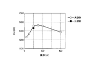
また、図5、図6は、実施例1~6の光電変換装置について、第二光電変換ユニットのn層の厚みを変えた際に得られた、光電変換効率(η)と開放電圧(Voc)の測定結果を示す。つまり、図5、図6は、各々、n層の厚み(横軸)に対して、η、Voc(縦軸)をプロットしたグラフである。
表1および図5、図6に示されるように、n層の厚さ(膜厚)が20~400Åの範囲において、開放電圧(Voc)が増大し、光電変換効率ηが増大する効果が認められる。特に、n層の厚さが100~200Åの範囲では、光電変換効率ηと開放電圧Vocの両方が、従来(比較例)の値を越える。なお、n層の厚さが400Å以上では、Vocが低下してしまう。これは、n層が光を吸収してしまい結晶質のシリコン系薄膜からなるi層側のJscが低下したためと推察される。その結果、光電変換効率ηも減少したと考えられる。したがって、第二光線変換ユニットを構成するn層の膜厚は、20~400Åの範囲が好適であり、100~200Åの範囲がより好ましい。
表1および図5、図6に示されるように、n層の厚さ(膜厚)が20~400Åの範囲において、開放電圧(Voc)が増大し、光電変換効率ηが増大する効果が認められる。特に、n層の厚さが100~200Åの範囲では、光電変換効率ηと開放電圧Vocの両方が、従来(比較例)の値を越える。なお、n層の厚さが400Å以上では、Vocが低下してしまう。これは、n層が光を吸収してしまい結晶質のシリコン系薄膜からなるi層側のJscが低下したためと推察される。その結果、光電変換効率ηも減少したと考えられる。したがって、第二光線変換ユニットを構成するn層の膜厚は、20~400Åの範囲が好適であり、100~200Åの範囲がより好ましい。
以上、本発明の光電変換装置及び光電変換装置の製造方法について説明してきたが、本発明はこれに限定されるものではなく、発明の趣旨を逸脱しない範囲で、適宜変更が可能である。
本発明は、光電変換装置及び光電変換装置の製造方法に広く適用可能である。
1 透明基板(基板)
2 透明導電膜
3 第一光電変換ユニット
4 第二光電変換ユニット
5 裏面電極
10A,10B(10) 光電変換装置
31 p型半導体層(第1のp型半導体層)
32 i型シリコン層(非晶質シリコン層、第1のi型半導体層)
33 n型半導体層(第1のn型半導体層)
41 p型半導体層(第2のp型半導体層)
42 i型シリコン層(結晶質シリコン層、第2のi型半導体層)
43 n型半導体層(第2のn型半導体層)
8 第一光電変換ユニット
81 p型半導体層(第3のp型半導体層)
82 i型シリコン層(結晶質シリコン層、第3のi型半導体層)
83 n型半導体層(第3のn型半導体層)
60 第一成膜装置
61 ロード室
62 p層成膜反応室
63(63a,63b,63c,63d) i層成膜反応室
64 n層成膜反応室
65 p層成膜反応室
66 アンロード室
70 第二成膜装置
71 ロード・アンロード室
72 in層成膜反応室
80 暴露装置
2 透明導電膜
3 第一光電変換ユニット
4 第二光電変換ユニット
5 裏面電極
10A,10B(10) 光電変換装置
31 p型半導体層(第1のp型半導体層)
32 i型シリコン層(非晶質シリコン層、第1のi型半導体層)
33 n型半導体層(第1のn型半導体層)
41 p型半導体層(第2のp型半導体層)
42 i型シリコン層(結晶質シリコン層、第2のi型半導体層)
43 n型半導体層(第2のn型半導体層)
8 第一光電変換ユニット
81 p型半導体層(第3のp型半導体層)
82 i型シリコン層(結晶質シリコン層、第3のi型半導体層)
83 n型半導体層(第3のn型半導体層)
60 第一成膜装置
61 ロード室
62 p層成膜反応室
63(63a,63b,63c,63d) i層成膜反応室
64 n層成膜反応室
65 p層成膜反応室
66 アンロード室
70 第二成膜装置
71 ロード・アンロード室
72 in層成膜反応室
80 暴露装置
Claims (6)
- 透明導電膜が形成された基板と;
前記透明導電膜の上に、アモルファスのシリコン系薄膜からなる、第1のp型半導体層と、第1の実質的に真性なi型半導体層と、第1のn型半導体層とを順に積層して形成されたpin型の第一光電変換ユニットと;
前記第一光電変換ユニットの上に、結晶質のシリコン系薄膜からなる第2のp型半導体層と第2の実質的に真性なi型半導体層と、アモルファスのシリコン系薄膜からなる第2のn型半導体層とを順に積層して形成されたpin型の第二光電変換ユニットと;
前記第二光電変換ユニットの上に形成された裏面電極と;
を備えることを特徴とする光電変換装置。 - 前記第2のn型半導体層の厚みが、20~400Åであることを特徴とする請求項1に記載の光電変換装置。
- 基板に形成された透明導電膜の上に、アモルファスのシリコン系薄膜からなりpin型の第一光電変換ユニットを構成する、第1のp型半導体層と、第1の実質的に真性なi型半導体層と、第1のn型半導体層とを順に形成し;
前記第1のn型半導体層の上に、結晶質のシリコン系薄膜からなりpin型の第二光電変換ユニットを構成する、第2のp型半導体層と、第2の実質的に真性なi型半導体層とを順に形成し;
前記第2のi型半導体層の上に、アモルファスのシリコン系薄膜からなり前記第二光電変換ユニットを構成する、第2のn型半導体層を形成し;
前記第2のn型半導体層の上に、裏面電極を形成する;
ことを特徴とする光電変換装置の製造方法。 - 透明導電膜が形成された基板と;
前記透明導電膜の上に、結晶質のシリコン系薄膜からなる第3のp型半導体層と第3の実質的に真性なi型半導体層と、アモルファスのシリコン系薄膜からなる第3のn型半導体層とを順に積層して形成されたpin型の第三光電変換ユニットと;
前記第三光電変換ユニットの上に形成された裏面電極と;
を備えることを特徴とする光電変換装置。 - 前記第3のn型半導体層の厚みが、20~400Åであることを特徴とする請求項4に記載の光電変換装置。
- 基板に形成された透明導電膜の上に、結晶質のシリコン系薄膜からなりpin型の第三光電変換ユニットを構成する、第3のp型半導体層と、第3の実質的に真性なi型半導体層とを順に形成し;
前記第3のi型半導体層の上に、アモルファスのシリコン系薄膜からなり前記第三光電変換ユニットを構成する、第3のn型半導体層を形成し;
前記第3のn型半導体層の上に、裏面電極を形成する;
ことを特徴とする光電変換装置の製造方法。
Priority Applications (1)
| Application Number | Priority Date | Filing Date | Title |
|---|---|---|---|
| JP2012509593A JPWO2011125878A1 (ja) | 2010-04-02 | 2011-03-31 | 光電変換装置及び光電変換装置の製造方法 |
Applications Claiming Priority (2)
| Application Number | Priority Date | Filing Date | Title |
|---|---|---|---|
| JP2010086181 | 2010-04-02 | ||
| JP2010-086181 | 2010-04-02 |
Publications (1)
| Publication Number | Publication Date |
|---|---|
| WO2011125878A1 true WO2011125878A1 (ja) | 2011-10-13 |
Family
ID=44762816
Family Applications (1)
| Application Number | Title | Priority Date | Filing Date |
|---|---|---|---|
| PCT/JP2011/058289 Ceased WO2011125878A1 (ja) | 2010-04-02 | 2011-03-31 | 光電変換装置及び光電変換装置の製造方法 |
Country Status (3)
| Country | Link |
|---|---|
| JP (1) | JPWO2011125878A1 (ja) |
| TW (1) | TW201145541A (ja) |
| WO (1) | WO2011125878A1 (ja) |
Citations (4)
| Publication number | Priority date | Publication date | Assignee | Title |
|---|---|---|---|---|
| JPH04192373A (ja) * | 1990-11-26 | 1992-07-10 | Canon Inc | 光起電力素子 |
| JP2000068533A (ja) * | 1998-08-25 | 2000-03-03 | Sharp Corp | 微結晶シリコン薄膜太陽電池及びその製造方法 |
| JP2006120745A (ja) * | 2004-10-20 | 2006-05-11 | Mitsubishi Heavy Ind Ltd | 薄膜シリコン積層型太陽電池 |
| WO2009069544A1 (ja) * | 2007-11-30 | 2009-06-04 | Kaneka Corporation | シリコン系薄膜光電変換装置 |
-
2011
- 2011-03-31 WO PCT/JP2011/058289 patent/WO2011125878A1/ja not_active Ceased
- 2011-03-31 JP JP2012509593A patent/JPWO2011125878A1/ja active Pending
- 2011-03-31 TW TW100111400A patent/TW201145541A/zh unknown
Patent Citations (4)
| Publication number | Priority date | Publication date | Assignee | Title |
|---|---|---|---|---|
| JPH04192373A (ja) * | 1990-11-26 | 1992-07-10 | Canon Inc | 光起電力素子 |
| JP2000068533A (ja) * | 1998-08-25 | 2000-03-03 | Sharp Corp | 微結晶シリコン薄膜太陽電池及びその製造方法 |
| JP2006120745A (ja) * | 2004-10-20 | 2006-05-11 | Mitsubishi Heavy Ind Ltd | 薄膜シリコン積層型太陽電池 |
| WO2009069544A1 (ja) * | 2007-11-30 | 2009-06-04 | Kaneka Corporation | シリコン系薄膜光電変換装置 |
Also Published As
| Publication number | Publication date |
|---|---|
| TW201145541A (en) | 2011-12-16 |
| JPWO2011125878A1 (ja) | 2013-07-11 |
Similar Documents
| Publication | Publication Date | Title |
|---|---|---|
| JP4940290B2 (ja) | 光電変換装置及びその製造方法 | |
| TWI722078B (zh) | 光電轉換裝置之製造方法 | |
| JP2011135053A (ja) | 光電変換装置及びその製造方法 | |
| JP2009038064A (ja) | 光電変換装置及びその製造方法 | |
| CN101779294B (zh) | 光电转换装置 | |
| KR101280036B1 (ko) | 광전 변환 장치의 제조 방법, 광전 변환 장치 및 광전 변환 장치의 제조 시스템 | |
| US20120015473A1 (en) | Photoelectric conversion device manufacturing method, photoelectric conversion device, photoelectric conversion device manufacturing system, and method for using photoelectric conversion device manufacturing system | |
| WO2010050035A1 (ja) | 光電変換装置の製造方法 | |
| JP4764469B2 (ja) | 光電変換装置及び光電変換装置の製造方法 | |
| WO2013168515A1 (ja) | 光電変換装置およびその製造方法 | |
| JP2008283075A (ja) | 光電変換装置の製造方法 | |
| TWI790245B (zh) | 光電轉換裝置之製造方法 | |
| WO2011125878A1 (ja) | 光電変換装置及び光電変換装置の製造方法 | |
| JP2011066213A (ja) | 光電変換装置及びその製造方法 | |
| JP4875566B2 (ja) | 光電変換装置の製造方法 | |
| WO2010146846A1 (ja) | 光電変換装置及び光電変換装置の製造方法 | |
| JP2007287926A (ja) | 集積化薄膜光電変換装置の製造方法および、その製造方法で得られうる集積化薄膜光電変換装置。 | |
| CN1310340C (zh) | 叠层型光电元件 | |
| JP5373045B2 (ja) | 光電変換装置 | |
| WO2011068197A1 (ja) | 光電変換装置及び光電変換装置の製造方法 | |
| JP2010283162A (ja) | 太陽電池及びその製造方法 | |
| WO2012057201A1 (ja) | 光電変換装置及び光電変換装置の製造方法 | |
| JP2010177582A (ja) | 光電変換装置の製造方法と光電変換装置、及び光電変換装置の製造システム | |
| JP2004071715A (ja) | 光起電力素子の製造方法及び光起電力素子 | |
| WO2010023948A1 (ja) | 光電変換装置の製造方法、光電変換装置、及び光電変換装置の製造システム |
Legal Events
| Date | Code | Title | Description |
|---|---|---|---|
| 121 | Ep: the epo has been informed by wipo that ep was designated in this application |
Ref document number: 11765778 Country of ref document: EP Kind code of ref document: A1 |
|
| WWE | Wipo information: entry into national phase |
Ref document number: 2012509593 Country of ref document: JP |
|
| NENP | Non-entry into the national phase |
Ref country code: DE |
|
| 122 | Ep: pct application non-entry in european phase |
Ref document number: 11765778 Country of ref document: EP Kind code of ref document: A1 |