WO2011125802A1 - 配線構造、表示装置、および半導体装置 - Google Patents
配線構造、表示装置、および半導体装置 Download PDFInfo
- Publication number
- WO2011125802A1 WO2011125802A1 PCT/JP2011/058141 JP2011058141W WO2011125802A1 WO 2011125802 A1 WO2011125802 A1 WO 2011125802A1 JP 2011058141 W JP2011058141 W JP 2011058141W WO 2011125802 A1 WO2011125802 A1 WO 2011125802A1
- Authority
- WO
- WIPO (PCT)
- Prior art keywords
- layer
- alloy
- semiconductor layer
- wiring structure
- amorphous silicon
- Prior art date
- Legal status (The legal status is an assumption and is not a legal conclusion. Google has not performed a legal analysis and makes no representation as to the accuracy of the status listed.)
- Ceased
Links
Images





Classifications
-
- H—ELECTRICITY
- H10—SEMICONDUCTOR DEVICES; ELECTRIC SOLID-STATE DEVICES NOT OTHERWISE PROVIDED FOR
- H10D—INORGANIC ELECTRIC SEMICONDUCTOR DEVICES
- H10D64/00—Electrodes of devices having potential barriers
- H10D64/01—Manufacture or treatment
- H10D64/011—Manufacture or treatment of electrodes ohmically coupled to a semiconductor
-
- H—ELECTRICITY
- H10—SEMICONDUCTOR DEVICES; ELECTRIC SOLID-STATE DEVICES NOT OTHERWISE PROVIDED FOR
- H10W—GENERIC PACKAGES, INTERCONNECTIONS, CONNECTORS OR OTHER CONSTRUCTIONAL DETAILS OF DEVICES COVERED BY CLASS H10
- H10W20/00—Interconnections in chips, wafers or substrates
- H10W20/40—Interconnections external to wafers or substrates, e.g. back-end-of-line [BEOL] metallisations or vias connecting to gate electrodes
- H10W20/41—Interconnections external to wafers or substrates, e.g. back-end-of-line [BEOL] metallisations or vias connecting to gate electrodes characterised by their conductive parts
- H10W20/425—Barrier, adhesion or liner layers
-
- H—ELECTRICITY
- H10—SEMICONDUCTOR DEVICES; ELECTRIC SOLID-STATE DEVICES NOT OTHERWISE PROVIDED FOR
- H10D—INORGANIC ELECTRIC SEMICONDUCTOR DEVICES
- H10D30/00—Field-effect transistors [FET]
- H10D30/60—Insulated-gate field-effect transistors [IGFET]
- H10D30/601—Insulated-gate field-effect transistors [IGFET] having lightly-doped drain or source extensions, e.g. LDD IGFETs or DDD IGFETs
-
- H—ELECTRICITY
- H10—SEMICONDUCTOR DEVICES; ELECTRIC SOLID-STATE DEVICES NOT OTHERWISE PROVIDED FOR
- H10D—INORGANIC ELECTRIC SEMICONDUCTOR DEVICES
- H10D30/00—Field-effect transistors [FET]
- H10D30/60—Insulated-gate field-effect transistors [IGFET]
- H10D30/67—Thin-film transistors [TFT]
- H10D30/6729—Thin-film transistors [TFT] characterised by the electrodes
- H10D30/6737—Thin-film transistors [TFT] characterised by the electrodes characterised by the electrode materials
-
- H—ELECTRICITY
- H10—SEMICONDUCTOR DEVICES; ELECTRIC SOLID-STATE DEVICES NOT OTHERWISE PROVIDED FOR
- H10D—INORGANIC ELECTRIC SEMICONDUCTOR DEVICES
- H10D30/00—Field-effect transistors [FET]
- H10D30/60—Insulated-gate field-effect transistors [IGFET]
- H10D30/67—Thin-film transistors [TFT]
- H10D30/674—Thin-film transistors [TFT] characterised by the active materials
- H10D30/6741—Group IV materials, e.g. germanium or silicon carbide
- H10D30/6743—Silicon
-
- H—ELECTRICITY
- H10—SEMICONDUCTOR DEVICES; ELECTRIC SOLID-STATE DEVICES NOT OTHERWISE PROVIDED FOR
- H10D—INORGANIC ELECTRIC SEMICONDUCTOR DEVICES
- H10D64/00—Electrodes of devices having potential barriers
- H10D64/01—Manufacture or treatment
- H10D64/011—Manufacture or treatment of electrodes ohmically coupled to a semiconductor
- H10D64/0111—Manufacture or treatment of electrodes ohmically coupled to a semiconductor to Group IV semiconductors
- H10D64/0112—Manufacture or treatment of electrodes ohmically coupled to a semiconductor to Group IV semiconductors using conductive layers comprising silicides
-
- H—ELECTRICITY
- H10—SEMICONDUCTOR DEVICES; ELECTRIC SOLID-STATE DEVICES NOT OTHERWISE PROVIDED FOR
- H10D—INORGANIC ELECTRIC SEMICONDUCTOR DEVICES
- H10D64/00—Electrodes of devices having potential barriers
- H10D64/60—Electrodes characterised by their materials
- H10D64/66—Electrodes having a conductor capacitively coupled to a semiconductor by an insulator, e.g. MIS electrodes
- H10D64/665—Electrodes having a conductor capacitively coupled to a semiconductor by an insulator, e.g. MIS electrodes the conductor comprising a layer of elemental metal contacting the insulator, e.g. tungsten or molybdenum
- H10D64/666—Electrodes having a conductor capacitively coupled to a semiconductor by an insulator, e.g. MIS electrodes the conductor comprising a layer of elemental metal contacting the insulator, e.g. tungsten or molybdenum the conductor further comprising additional layers
-
- H—ELECTRICITY
- H10—SEMICONDUCTOR DEVICES; ELECTRIC SOLID-STATE DEVICES NOT OTHERWISE PROVIDED FOR
- H10P—GENERIC PROCESSES OR APPARATUS FOR THE MANUFACTURE OR TREATMENT OF DEVICES COVERED BY CLASS H10
- H10P14/00—Formation of materials, e.g. in the shape of layers or pillars
- H10P14/40—Formation of materials, e.g. in the shape of layers or pillars of conductive or resistive materials
- H10P14/42—Formation of materials, e.g. in the shape of layers or pillars of conductive or resistive materials using a gas or vapour
- H10P14/43—Chemical deposition, e.g. chemical vapour deposition [CVD]
-
- H—ELECTRICITY
- H10—SEMICONDUCTOR DEVICES; ELECTRIC SOLID-STATE DEVICES NOT OTHERWISE PROVIDED FOR
- H10P—GENERIC PROCESSES OR APPARATUS FOR THE MANUFACTURE OR TREATMENT OF DEVICES COVERED BY CLASS H10
- H10P14/00—Formation of materials, e.g. in the shape of layers or pillars
- H10P14/60—Formation of materials, e.g. in the shape of layers or pillars of insulating materials
- H10P14/63—Formation of materials, e.g. in the shape of layers or pillars of insulating materials characterised by the formation processes
- H10P14/6302—Non-deposition formation processes
- H10P14/6316—Formation by nitridation, e.g. nitridation of the substrate
-
- H—ELECTRICITY
- H10—SEMICONDUCTOR DEVICES; ELECTRIC SOLID-STATE DEVICES NOT OTHERWISE PROVIDED FOR
- H10P—GENERIC PROCESSES OR APPARATUS FOR THE MANUFACTURE OR TREATMENT OF DEVICES COVERED BY CLASS H10
- H10P58/00—Singulating wafers or substrates into multiple chips, i.e. dicing
-
- H—ELECTRICITY
- H10—SEMICONDUCTOR DEVICES; ELECTRIC SOLID-STATE DEVICES NOT OTHERWISE PROVIDED FOR
- H10W—GENERIC PACKAGES, INTERCONNECTIONS, CONNECTORS OR OTHER CONSTRUCTIONAL DETAILS OF DEVICES COVERED BY CLASS H10
- H10W20/00—Interconnections in chips, wafers or substrates
- H10W20/01—Manufacture or treatment
-
- H—ELECTRICITY
- H10—SEMICONDUCTOR DEVICES; ELECTRIC SOLID-STATE DEVICES NOT OTHERWISE PROVIDED FOR
- H10W—GENERIC PACKAGES, INTERCONNECTIONS, CONNECTORS OR OTHER CONSTRUCTIONAL DETAILS OF DEVICES COVERED BY CLASS H10
- H10W20/00—Interconnections in chips, wafers or substrates
- H10W20/01—Manufacture or treatment
- H10W20/031—Manufacture or treatment of conductive parts of the interconnections
- H10W20/032—Manufacture or treatment of conductive parts of the interconnections of conductive barrier, adhesion or liner layers
- H10W20/055—Manufacture or treatment of conductive parts of the interconnections of conductive barrier, adhesion or liner layers by formation methods other than physical vapour deposition [PVD], chemical vapour deposition [CVD] or liquid deposition
-
- H—ELECTRICITY
- H10—SEMICONDUCTOR DEVICES; ELECTRIC SOLID-STATE DEVICES NOT OTHERWISE PROVIDED FOR
- H10D—INORGANIC ELECTRIC SEMICONDUCTOR DEVICES
- H10D30/00—Field-effect transistors [FET]
- H10D30/01—Manufacture or treatment
- H10D30/021—Manufacture or treatment of FETs having insulated gates [IGFET]
- H10D30/0223—Manufacture or treatment of FETs having insulated gates [IGFET] having source and drain regions or source and drain extensions self-aligned to sides of the gate
- H10D30/0227—Manufacture or treatment of FETs having insulated gates [IGFET] having source and drain regions or source and drain extensions self-aligned to sides of the gate having both lightly-doped source and drain extensions and source and drain regions self-aligned to the sides of the gate, e.g. lightly-doped drain [LDD] MOSFET or double-diffused drain [DDD] MOSFET
-
- H—ELECTRICITY
- H10—SEMICONDUCTOR DEVICES; ELECTRIC SOLID-STATE DEVICES NOT OTHERWISE PROVIDED FOR
- H10D—INORGANIC ELECTRIC SEMICONDUCTOR DEVICES
- H10D86/00—Integrated devices formed in or on insulating or conducting substrates, e.g. formed in silicon-on-insulator [SOI] substrates or on stainless steel or glass substrates
- H10D86/40—Integrated devices formed in or on insulating or conducting substrates, e.g. formed in silicon-on-insulator [SOI] substrates or on stainless steel or glass substrates characterised by multiple TFTs
- H10D86/441—Interconnections, e.g. scanning lines
-
- H—ELECTRICITY
- H10—SEMICONDUCTOR DEVICES; ELECTRIC SOLID-STATE DEVICES NOT OTHERWISE PROVIDED FOR
- H10D—INORGANIC ELECTRIC SEMICONDUCTOR DEVICES
- H10D86/00—Integrated devices formed in or on insulating or conducting substrates, e.g. formed in silicon-on-insulator [SOI] substrates or on stainless steel or glass substrates
- H10D86/40—Integrated devices formed in or on insulating or conducting substrates, e.g. formed in silicon-on-insulator [SOI] substrates or on stainless steel or glass substrates characterised by multiple TFTs
- H10D86/60—Integrated devices formed in or on insulating or conducting substrates, e.g. formed in silicon-on-insulator [SOI] substrates or on stainless steel or glass substrates characterised by multiple TFTs wherein the TFTs are in active matrices
Definitions
- the present invention relates to a flat panel display (display device) such as a liquid crystal display or an organic EL display; a semiconductor device such as a ULSI (Ultra Large Scale Integrated Circuit), an ASIC (Application Specific Integrated Circuit), a FET (Field Effect Transistor), or a diode;
- a wiring structure including a Cu alloy film as a wiring material In the following description, the wiring in the thin film transistor of the liquid crystal display device will be described as an example, but the present invention is not limited to this.
- An active matrix liquid crystal display device such as a liquid crystal display uses a thin film transistor (hereinafter referred to as a TFT) as a switching element, a transparent pixel electrode, a wiring portion such as a gate wiring and source / drain wiring, and amorphous silicon.
- a TFT substrate having a semiconductor layer such as (a-Si) or polycrystalline silicon (p-Si); a counter substrate having a common electrode disposed opposite to the TFT substrate at a predetermined interval; and a TFT substrate. And a liquid crystal layer filled between the counter substrate and the counter substrate.
- an aluminum (Al) alloy film has been used as a wiring material such as a gate wiring and a source / drain wiring.
- Al aluminum
- Cu copper
- a Cu-based alloy When pure Cu or a Cu alloy (hereinafter collectively referred to as a Cu-based alloy) is used as a wiring material, it is usually between Patent Documents 1 to 7 between the Cu-based alloy wiring film and the TFT semiconductor layer. As described in the above, a barrier metal layer made of a refractory metal such as Mo, Cr, Ti, or W is provided. There are two main reasons for this.
- a subsequent process for example, a film forming process of an insulating layer formed on the TFT, sintering, Cu in the Cu-based alloy wiring film diffuses into the semiconductor layer due to the thermal history in the thermal process (such as annealing), and the TFT characteristics are degraded, or the contact resistance between the Cu-based alloy wiring film and the semiconductor layer is increased.
- a subsequent process for example, a film forming process of an insulating layer formed on the TFT, sintering, Cu in the Cu-based alloy wiring film diffuses into the semiconductor layer due to the thermal history in the thermal process (such as annealing), and the TFT characteristics are degraded, or the contact resistance between the Cu-based alloy wiring film and the semiconductor layer is increased.
- a film forming apparatus for forming a barrier metal in addition to a film forming apparatus for forming a Cu-based alloy wiring film, a film forming apparatus for forming a barrier metal is separately required. Specifically, a film forming apparatus (typically a cluster tool in which a plurality of film forming chambers are connected to a transfer chamber) each equipped with an extra film forming chamber for forming a barrier metal layer must be used. This causes an increase in manufacturing cost and a decrease in productivity.
- Patent Document 8 is cited as a technique in which the barrier metal layer as described above is omitted.
- Patent Document 8 as a direct contact technique between a Cu-based alloy film and a semiconductor layer, a material comprising a nitrogen-containing layer or an oxygen-nitrogen-containing layer and a Cu-based alloy film, wherein N (nitrogen) of the nitrogen-containing layer, or A wiring structure in which nitrogen or oxygen in the oxygen-nitrogen containing layer is bonded to Si in the semiconductor layer is disclosed.
- the present invention has been made in view of the above circumstances, and its purpose is to achieve excellent low contact resistance even if a barrier metal layer normally provided between a Cu-based alloy wiring film and a semiconductor layer is omitted. And providing a wiring structure having excellent adhesion between the Cu-based alloy wiring film and the semiconductor layer.
- a wiring structure comprising a semiconductor layer and a Cu alloy layer on a substrate in order from the substrate side, (N, C, F, O) layer containing at least one element selected from the group consisting of nitrogen, carbon, fluorine, and oxygen in order from the substrate side between the semiconductor layer and the Cu alloy layer And a Cu—Si diffusion layer containing Cu and Si, and any element of nitrogen, carbon, fluorine and oxygen constituting the (N, C, F, O) layer is Bonded to Si of the semiconductor layer;
- the Cu alloy layer is a Cu—X alloy layer containing at least one alloy component X selected from the group consisting of Zn, Ni, Ti, Al, Mg, Ca, W, Nb and Mn in this order from the substrate side.
- Wiring structure [2] The wiring structure according to [1], wherein the X content in the first layer which is the Cu—X alloy layer is 0.5 to 20 atomic%. [3] The wiring structure according to [1] or [2], wherein the film thickness of the first layer which is the Cu—X alloy layer is 5 to 150 nm and is 50% or less with respect to the total film thickness of the Cu alloy layer. .
- the film thickness x (nm) of the first layer, which is the Cu—X alloy layer, and the X content y (atomic%) satisfy the relationship of the following formula (1) [1] to [3] Wiring structure as described in any one of these. y ⁇ ⁇ 0.085x + 8.0 (1)
- the Cu—Si diffusion layer is obtained by forming the (N, C, F, O) layer, the semiconductor layer, and the Cu alloy layer in this order, and then applying a thermal history.
- the present invention is a direct contact technology capable of directly contacting a Cu alloy layer with a semiconductor layer, and not only has excellent contact resistance between the Cu alloy layer and the semiconductor layer, but also has good productivity.
- it is possible to provide a technique with a further increased process margin. Specifically, it is difficult to be affected by variations in various process conditions (variation in equipment performance, instability, unexpected contamination, contamination that is difficult to control, etc.), and it is not necessary to manage extremely strict conditions. It is possible to provide technology that is not easily restricted.
- the first layer of the Cu alloy layer is Cu— containing X (X is at least one selected from the group consisting of Zn, Ni, Ti, Al, Mg, Ca, W, Nb and Mn) as an alloy component.
- the X alloy layer (first layer) and the second layer are pure Cu or a Cu alloy containing Cu as a main component and having a lower electrical resistivity than the first layer, the semiconductor While improving the adhesiveness with a layer and low contact resistance, the raise of the electrical resistivity as the whole Cu alloy layer can be suppressed.
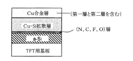
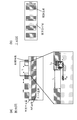
- FIG. 1A is a schematic cross-sectional explanatory diagram showing a configuration of a TFT according to the first embodiment of the present invention.
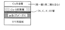
- FIG. 1B is a schematic cross-sectional explanatory diagram showing the configuration of the TFT according to the first embodiment of the present invention.
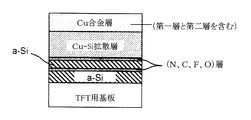
- FIG. 1C is a schematic cross-sectional explanatory diagram showing the configuration of the TFT according to the first embodiment of the present invention.
- FIG. 2 is a schematic cross-sectional explanatory view showing a configuration of a TFT according to the second embodiment of the present invention.
- FIG. 3 is a schematic process diagram for explaining the process of the wiring structure of the present invention.
- FIG. 4 is a schematic cross-sectional explanatory view showing the structure of a MOSFET according to the third embodiment of the present invention.
- FIG. 5 is a process diagram illustrating each process of the wiring structure according to the third embodiment of the present invention.
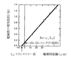
- FIG. 6 is a graph showing the relationship between the distance between electrodes and the electrical resistance.
- FIGS. 7A and 7B are diagrams for explaining the principle of contact resistance measurement by the TLM element.
- 8A to 8K are process diagrams for explaining a MOSFET manufacturing process.
- FIG. 9 is a graph showing the results of the adhesion evaluation test and the relationship between the film thickness of the first layer and the Mn content in the first layer.
- FIG. 10 is a graph showing the relationship between the thickness of the second semiconductor layer and the electrical resistivity of the entire Cu alloy layer (first layer + second layer).
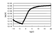
- FIG. 11 is a graph showing Ids-Vg characteristics of a TFT to which the wiring structure of the present invention is applied.
- the present invention relates to a direct contact technique capable of directly contacting a Cu-based alloy film and a semiconductor layer. Specifically, the invention is completed as a result of repeated studies mainly from the viewpoints of productivity and adhesion, based on Patent Document 8 described above. Note that the contents of Patent Document 8 are incorporated herein by reference.
- Patent Document 8 the invention of Patent Document 8 was found to cause the following problems.
- a plasma CVD apparatus under vacuum
- a semiconductor layer and a nitrogen-containing layer or an oxygen-nitrogen-containing layer are formed in a semiconductor layer forming chamber, and then transferred to a dedicated chamber (under vacuum) to form a Cu-based alloy film by sputtering or the like. It is necessary.
- the wiring structure in the present invention is a Cu— containing Cu and Si on the (N, C, F, O) layer as shown in FIG. 1A and the like. It has a great feature in that it has a laminated structure in which a Si diffusion layer is formed.
- the Cu—Si diffusion layer is formed by sequentially forming a (N, C, F, O) layer represented by a nitrogen-containing layer and the like, followed by a semiconductor layer and a Cu alloy layer.
- the formation of the Cu-based alloy film is preferably further promoted by a thermal history applied in the TFT manufacturing process, and is generally heat treated at 150 ° C. or higher (preferably 180 ° C. or higher).
- the Cu inside is obtained by diffusing into Si in the semiconductor layer.
- the Cu—Si diffusion layer thus obtained is composed of Cu in the Cu alloy layer and Si of the semiconductor layer, and acts as a cover layer that protects the (N, C, F, O) layer from the atmosphere.
- the Cu—Si diffusion layer may be directly formed on the (N, C, F, O) layer as shown in FIG. 1A, but is not limited thereto.
- the method for manufacturing the wiring structure according to the present invention does not directly form a Cu alloy layer on the nitrogen-containing layer as in Patent Document 8, but as shown in the schematic process diagram of FIG.
- a semiconductor layer is further formed on the (N, C, F, O) layer continuously in the same chamber.
- the Cu-based alloy film is transferred to a Cu alloy film-dedicated chamber, and then a TFT is manufactured by a known method.
- the thermal history changes to a Cu—Si diffusion layer, and the problems of degradation of TFT characteristics and contact resistance due to contamination of the (N, C, F, O) layer, or variations thereof are resolved.
- an (N, C, F, O) layer is disclosed as a barrier layer having a function of preventing mutual diffusion between the Cu alloy layer and the semiconductor layer directly formed on the TFT substrate.
- a nitrogen-containing layer and an oxygen-nitrogen-containing layer are disclosed as the barrier layer.
- the above-described action can be achieved by a layer containing carbon or fluorine.
- the (N, C, F, O) layers containing at least one element selected from the group consisting of nitrogen, carbon, fluorine, and oxygen are all nitrogen-containing layers and oxygen-nitrogen-containing layers. Experiments have confirmed that substantially similar results are obtained.
- the technique of Patent Document 8 is further developed in that the (N, C, F, O) layer is used as a barrier layer.
- the Cu alloy layer in the present invention has a laminated structure including a first layer and a second layer, and the first layer has an alloy component X (X is Zn, Ni, Ti, Al, Mg, Ca, W) , At least one selected from the group consisting of Nb and Mn).
- the first layer that is in direct contact with the semiconductor layer is made of a Cu alloy containing an alloy element that contributes to improving the adhesion, thereby improving the adhesion with the semiconductor layer. These X elements do not increase the contact resistance between the Cu alloy layer and the semiconductor layer.
- the second layer laminated on the first layer is composed of an element having a low electrical resistivity (pure Cu or a Cu alloy having a low electrical resistivity comparable to that of pure Cu).
- the electrical resistivity of the entire Cu alloy layer is reduced. That is, by using the laminated structure defined in the present invention, it is possible to effectively maximize the original characteristics of Cu that the electrical resistivity is lower than that of Al, and also with the semiconductor layer that was a defect of Cu. Low adhesion can also be eliminated.
- the present invention is a technique that is further improved on the basis of the technique of Patent Document 8, and Patent Document 8 may be referred to for a method of forming a nitrogen-containing layer and the like.
- Patent Document 8 differences from Patent Document 8 will be mainly described.
- the wiring structure of the present invention is a wiring structure including a semiconductor layer and a Cu alloy layer on a substrate in order from the substrate side, and a nitrogen layer in order from the substrate side between the semiconductor layer and the Cu alloy layer.
- Such a laminated structure may be provided at least between the semiconductor layer and the Cu alloy layer. For example, as shown in FIGS.
- the above laminated structure is provided directly on the semiconductor layer. Also good. Further, as shown in FIG. 2, a plurality of (N, C, F, O) layers may be provided, and in order from the substrate side, a semiconductor layer, an (N, C, F, O) layer, and a semiconductor layer are provided. In addition, embodiments having the above laminated structure are also included in the scope of the present invention. The present invention is not limited to these embodiments.
- the wiring structure of the present invention can be used for source / drain electrodes, TAB connection electrodes, and the like, and can also be applied to display devices such as liquid crystal displays and organic EL displays, and semiconductor devices such as ULSIs, ASICs, FETs, and diodes. is there.
- TFT embodiments 1 and 2 will be described as a representative example of a display device to which the wiring structure of the present invention is applied
- MOSFET embodiment 3 will be described as a representative example of a semiconductor layer.
- the type of the semiconductor layer may be any of hydrogenated amorphous silicon, amorphous silicon, microcrystalline silicon, polycrystalline silicon, or single crystal silicon.
- a semiconductor layer formed on the (N, C, F, O) layer, and the (N, C, F, O) layer is finally protected from the atmosphere by the subsequent thermal history.
- a semiconductor layer that can be changed to a Cu—Si diffusion layer to be obtained is called a “second semiconductor layer”, and a semiconductor layer formed directly on the TFT substrate is called a “first semiconductor layer”.
- FIG. 1A A first embodiment of a TFT according to the present invention is shown in FIG. 1A.
- FIG. 1A has a first semiconductor layer on a TFT substrate, and has a two-layer laminated structure including an (N, C, F, O) layer and a Cu—Si diffusion layer directly on the first semiconductor layer. And a Cu alloy layer (including a first layer and a second layer) is directly formed thereon.
- a second semiconductor layer and then a Cu alloy layer (laminated structure) are formed, and then a thermal history of about 150 ° C. or higher is applied. Can be obtained.
- the (N, C, F, O) layer contains at least one element of nitrogen, carbon, fluorine, and oxygen. Since the (N, C, F, O) layer is formed so as to substantially cover the entire surface of the semiconductor layer, interdiffusion of Cu and Si at the interface between the Cu alloy layer and the first semiconductor layer is prevented. It works effectively as a barrier.
- a nitrogen-containing layer is preferable. Specifically, nitrogen, carbon, fluorine and oxygen constituting the above layer are bonded to Si of the first semiconductor layer and mainly contain Si nitride, Si carbide, Si fluoride, and Si oxide. Yes.
- the Si nitride, the Si carbide, and the Si fluoride may further contain oxygen.
- the Si nitride may include a compound compound of Si oxynitride that further contains oxygen.
- the oxygen-containing composite compound such as Si oxynitride is obtained by combining with oxygen (O) that is inevitably introduced in the formation process of the nitrogen-containing layer, for example.
- the total area density of nitrogen atoms, carbon atoms, fluorine atoms, and oxygen atoms contained in the (N, C, F, O) layer is the effective bond of the first semiconductor layer material (typically Si). It is preferable that the surface density is equal to or higher than the surface density of the effective bond.
- the surface density is equal to or higher than the surface density of the effective bond.
- an (N, C, F, O) layer such as a nitrogen-containing layer.
- dangling bonds existing on the surface of the semiconductor layer are preferably bonded to each element constituting the layer.
- Effective bond means a bond that can be arranged on the surface of the semiconductor layer in consideration of steric hindrance of nitrogen atom, carbon atom, fluorine atom, oxygen atom, and “effective bond area density”
- the surface density when the entire surface of the semiconductor layer is covered with an (N, C, F, O) layer is meant.
- the surface density of the effective bond varies depending on the type of semiconductor material, but in the case of silicon, for example, it varies slightly depending on the crystal plane orientation, but is generally in the range of 10 14 cm ⁇ 2 to 2 ⁇ 10 16 cm ⁇ 2 . Is in.
- the nitrogen of the nitrogen-containing layer preferably has an area density (N1) of 10 14 cm ⁇ 2 or more and 2 ⁇ 10 16 cm ⁇ 2 or less at the interface in contact with the first semiconductor layer.
- N1 area density
- the lower limit of the surface density of nitrogen is more preferably 2 ⁇ 10 14 cm -2, even more preferred 4 ⁇ 10 14 cm -2.
- the carbon of the carbon-containing layer at the interface in contact with the semiconductor layer preferably has a 10 14 cm -2 or more 2 ⁇ 10 16 cm -2 or less of the surface density (C1), 2 ⁇ 10 14 cm -2 or more, and even more preferred 4 ⁇ 10 14 cm -2 or more.
- the fluorine of the fluorine-containing layer has an area density (F1) of 10 14 cm ⁇ 2 or more and 2 ⁇ 10 16 cm ⁇ 2 or less at the interface in contact with the first semiconductor layer. Is preferably 2 ⁇ 10 14 cm ⁇ 2 or more, more preferably 4 ⁇ 10 14 cm ⁇ 2 or more.
- the oxygen of the oxygen-containing layer also has an areal density (O1) of 10 14 cm ⁇ 2 or more and 2 ⁇ 10 16 cm ⁇ 2 or less at the interface in contact with the first semiconductor layer, as described above. It is preferably 2 ⁇ 10 14 cm ⁇ 2 or more, more preferably 4 ⁇ 10 14 cm ⁇ 2 or more.
- the (N, C, F, O) layer may have at least one layer including a Si—N bond, a Si—C bond, a Si—F bond, and a Si—O bond.
- the distance (atomic spacing) between Si and N in the Si—N bond is about 0.18 nm, substantially preferably 0.2 nm or more, and more preferably 0.3 nm or more.
- the surface density (N1) of nitrogen in the nitrogen-containing layer becomes too high, the insulating Si nitride contained in the nitrogen-containing layer also increases, which may increase the electrical resistance and degrade the TFT performance.
- the upper limit of the surface density of nitrogen in the nitrogen-containing layer is more preferably 1 ⁇ 10 16 cm ⁇ 2 .
- the distance (atomic spacing) between Si and C of Si—C bond is about 0.19 nm, substantially preferably 0.2 mm or more, and more preferably 0.3 nm or more.
- the upper limit of the surface density of carbon in the carbon-containing layer is more preferably 1 ⁇ 10 16 cm ⁇ 2 .
- the distance (atomic spacing) between Si and F in the Si—F bond is about 0.16 nm, substantially preferably 0.18 nm or more, and more preferably 0.25 nm or more.
- the upper limit of the surface density of fluorine in the fluorine-containing layer is more preferably 1 ⁇ 10 16 cm ⁇ 2 .
- the distance (atomic spacing) between Si and O in the Si—O bond is about 0.13 nm, substantially preferably 0.15 nm or more, and more preferably 0.2 nm or more.
- the upper limit of the surface density of oxygen in the oxygen-containing layer is more preferably 1 ⁇ 10 16 cm ⁇ 2 .
- N1, carbon surface density (C1), fluorine surface density (F1), and oxygen surface density (O1) of the (N, C, F, O) layer are, for example, RBS (Rutherford Backscattering (spectrometry, Rutherford backscattering spectroscopy)).
- the (N, C, F, O) layer is an (N, C, F) layer excluding O and contains an oxygen-containing compound such as Si oxynitride (for example, Si nitride)
- Si oxynitride for example, Si nitride
- the total area density of each element constituting the layer satisfies the above requirements and the area density of each element (N1, C1, F1).
- the surface density of oxygen (O1) (N1 + C1 + F1) / O1 is preferably 1.0 or more, which further enhances the TFT characteristics.
- Nitrogen-containing compounds such as Si nitride and oxygen-containing compounds such as Si oxynitride are inherently insulators, but the thickness of the (N, C, F, O) layer is as described later. In general, the electrical resistance can be kept low because the thickness is as thin as 0.18 nm to 5 nm.
- the TFT characteristics are affected by the ratio (N1 + C1 + F1) / O1, and in order to obtain more excellent TFT characteristics, the ratio (N1 + C1 + F1) / O1 is increased to 1.0 or more. It turned out to be good.
- the ratio of (N1 + C1 + F1) / O1 is preferably as large as possible.
- the ratio is more preferably 1.05 or more, and further preferably 1.1 or more.
- the ratio of (N1 + C1 + F1) / O1 is adjusted, for example, by appropriately controlling plasma generation conditions such as plasma gas pressure, gas composition, and processing temperature when forming a nitrogen-containing layer using plasma nitriding. Can do.
- the thickness of the (N, C, F, O) layer is generally in the range of 0.18 nm to 5 nm.
- the (N, C, F, O) layer is useful as a barrier layer for preventing mutual diffusion of Cu and Si at the interface between the Cu alloy layer and the first semiconductor layer. Since the (N, C, F, O) layer tends to be an insulator, if it is too thick, the electrical resistance becomes extremely high and the TFT performance deteriorates.
- the thickness of the (N, C, F, O) layer within the above range, the increase in electrical resistance due to the formation of the (N, C, F, O) layer does not adversely affect the TFT performance. It is suppressed in.
- the thickness of the (N, C, F, O) layer is generally more preferably 3 nm or less, further preferably 2 nm or less, and even more preferably 1 nm or less.
- the thickness of the (N, C, F, O) layer can be determined by various physical analysis techniques. For example, in addition to the RBS method described above, XPS (X-ray photoelectron spectroscopy) method, SIMS (secondary ion) Mass spectrometry) method, GD-OES (High Frequency Glow Discharge Optical Emission Spectroscopy) method and the like can be used.
- the upper limit and the lower limit of the thickness of the (N, C, F, O) layer can be arbitrarily combined to make the range.
- the maximum value of the ratio of the number of atoms of each element constituting the (N, C, F, O) layer to the number of Si atoms ((N, C, F, O) / Si) is 0.5 or more and 1.5 It is preferable to be within the following range. Thereby, the barrier action by the (N, C, F, O) layer can be effectively exhibited without deteriorating the TFT characteristics.
- the maximum value of the ratio is more preferably 0.6 or more, and further preferably 0.7 or more. The above ratio can be adjusted, for example, by controlling the plasma irradiation time within a range of about 5 seconds to 10 minutes.
- the above ratio is calculated by analyzing elements (N, C, F, O and Si) in the depth direction of the (N, C, F, O) layer by the RBS method.
- the upper limit and the lower limit of the maximum value of the ratio can be arbitrarily combined to make the range.
- the nitrogen-containing layer may be formed using a thermal nitridation method or an amination method.
- a gas containing at least one of nitrogen, carbon, fluorine, and oxygen can be used.
- gases include nitrogen-containing gases such as N 2 , NH 3 , N 2 O, and NO; nitrogen and fluorine-containing gases such as NF 3 ; CO, CO 2 , and hydrocarbon-based gases (for example, CH 4 , C 2 Carbon-containing gases such as H 4 and C 2 H 2 ; carbon-fluorine containing gases such as fluorine-containing gases (for example, CF 4 and C 4 F 8 ) and CHF 3 ; oxygen (O 2 ), oxygen An oxygen-containing gas such as an oxidizing gas containing atoms (for example, O 3 ) can be used. These gases can be used alone or as a mixed gas.
- a method for supplying at least one of nitrogen, carbon, fluorine, and oxygen from the plasma source containing the gas to the surface of the semiconductor layer for example, a method in which a semiconductor layer is installed in the vicinity of the plasma source can be given. It is done.
- the distance between the plasma source and the semiconductor layer may be appropriately set according to various parameters such as plasma type, plasma generation power, pressure, temperature, etc., but generally several cm from the state of contact with the plasma. A distance of up to 10 cm can be used.
- In the vicinity of such plasma there are atoms with high energy.
- nitrogen, carbon, fluorine, oxygen, etc. to the surface of the semiconductor layer by this high energy, nitride, carbide, fluorine are supplied to the semiconductor surface. Compounds, oxides, etc. can be formed.
- an ion implantation method may be used.
- ions are accelerated by an electric field and can be moved over a long distance, so that the distance between the plasma source and the semiconductor layer can be arbitrarily set.
- This method can be realized by using a dedicated ion implantation apparatus, but a plasma ion implantation method is preferably used.
- the plasma ion implantation method is a technique for uniformly performing ion implantation by applying a negative high voltage pulse to a semiconductor layer installed in the vicinity of plasma.
- oxygen in addition to the above method, when UV irradiation is performed on the surface of the semiconductor layer, highly reactive ozone is generated to oxidize the semiconductor surface, so that oxygen can be supplied to the semiconductor layer. Further, oxygen can be supplied even if the semiconductor surface is subjected to an acid immersion treatment such as hydrogen peroxide or nitric acid.
- the apparatus, chamber, temperature, and gas composition used for forming the layer are as follows. It is preferable to carry out such control.
- the apparatus is preferably performed in the same apparatus as the semiconductor layer forming apparatus, and more preferably in the same chamber of the same apparatus. This eliminates the need for extra work to be processed between devices or between devices.
- the temperature it is preferable to carry out at substantially the same temperature as the semiconductor layer deposition temperature (which may include a range of about ⁇ 10 ° C.), whereby the adjustment time associated with temperature fluctuations can be omitted.
- a gas containing at least one element selected from the group consisting of nitrogen, carbon, fluorine, and oxygen (the aforementioned nitrogen-containing gas, carbon-containing gas, fluorine-containing gas, oxygen-containing gas) (N, C, F, O) layer may be formed using a gas or the like, or (ii) containing at least one element selected from the group consisting of nitrogen, carbon, fluorine, and oxygen A (N, C, F, O) layer may be formed using a mixed gas of a gas and a source gas used for forming the semiconductor layer, or (iii) made of nitrogen, carbon, fluorine, and oxygen
- the (N, C, F, O) layer may be formed using a mixed gas of a gas containing at least one element selected from the group and a reducing gas.
- a nitrogen-containing layer when forming a nitrogen-containing layer, it may be performed using only a nitrogen-containing gas (N 2 , NH 3 , NF 3, etc.) containing at least nitrogen as in (i) above, but the above (ii) As described above, a mixed gas of a nitrogen-containing gas and a raw material gas (SiH 4 ) used for forming the semiconductor layer is preferable.
- a nitrogen-containing layer is formed using only a nitrogen-containing gas, it is necessary to temporarily remove all the semiconductor layer forming gas used in order to purge the inside of the chamber after the formation of the semiconductor layer. If it is performed under the condition of gas, it is not necessary to eliminate the gas, so that the processing time can be shortened.
- a gas containing at least one element selected from the group consisting of nitrogen, carbon, fluorine, and oxygen hereinafter abbreviated as “(N, C, F, O) gas”, particularly containing nitrogen) Gas
- a raw material gas used for forming the semiconductor layer hereinafter referred to as “semiconductor raw material gas”
- semiconductor raw material gas preferably has a flow rate ratio ((N, C, F, O) gas / semiconductor raw material gas) of 0.10. It is preferable to control the value to 15 or less. This effectively exhibits the effect of shortening the processing time, increases the insulating properties of the barrier layer, reduces TFT characteristics (on-current / off-current), and reduces contact resistance. Can be prevented.
- a more preferable flow rate ratio of ((N, C, F, O) gas / semiconductor raw material gas) is 0.3 or more and 10 or less, and a more preferable flow rate ratio is 0.5 or more and 7 or less.
- the upper limit and the lower limit of the flow rate ratio can be arbitrarily combined to make the range.
- the gas composition is preferably a mixed gas of the above-described nitrogen-containing gas and reducing element-containing gas as described in (iii) above, whereby oxidation of the semiconductor layer can be more effectively suppressed.
- the reducing element include NH 3 and H 2 .
- NH 3 not only has a reducing action, but also acts as a nitrogen-containing gas, so it can be used alone or in combination with H 2 .
- the Cu—Si diffusion layer is obtained at the time when the Cu alloy layer is formed, and preferably the formation thereof is further promoted by the thermal history applied thereafter in the TFT manufacturing process. It is obtained by diffusing Cu inside to Si in the second semiconductor layer.
- the Cu—Si diffusion layer has an action of protecting the (N, C, F, O) layer from contamination by the atmosphere.
- the thickness of the Cu—Si diffusion layer is preferably adjusted as appropriate according to required TFT characteristics, and is preferably 0.2 nm or more and 200 nm or less. Specifically, the thickness is preferably larger than the thickness corresponding to one Cu—Si atom (about 0.2 nm), and is preferably 200 nm or less from the viewpoint of being as thin as possible from the viewpoint of TFT manufacturing.
- the second semiconductor layer has a function of protecting the (N, C, F, O) layer from contamination by the atmosphere by diffusing Cu in the Cu alloy layer to form a Cu—Si diffusion layer.
- the electrical resistivity of the entire Cu alloy layer may increase.
- the thickness of the second semiconductor layer is preferably 45 nm or less.
- the Cu alloy layer of the present invention has a laminated structure including a first layer and a second layer in order from the substrate side.
- the first layer is Cu—X containing X (X is at least one selected from the group consisting of Zn, Ni, Ti, Al, Mg, Ca, W, Nb and Mn) as an alloy component. Alloy layer.
- X is at least one selected from the group consisting of Zn, Ni, Ti, Al, Mg, Ca, W, Nb and Mn
- Alloy layer Such a first layer is intended to include a semiconductor layer (including a semiconductor layer that changes to a Cu—Si diffusion layer without a barrier metal layer interposed therebetween, and thus the first semiconductor layer and the second semiconductor layer.
- the adhesiveness between the Cu alloy layer and the semiconductor layer in the present invention is the same), and the low contact resistance with the semiconductor layer can be achieved.
- These X elements are selected as elements that dissolve in the Cu metal but do not dissolve in the Cu oxide film.
- these elements When a Cu alloy in which these elements are dissolved is oxidized by heat treatment during the film formation process, the elements diffuse and concentrate at the grain boundaries and interfaces, and the adhesion to the semiconductor layer is improved by the concentrated layer. I think that. Further, these elements can exhibit the above-mentioned adhesion without inhibiting the usefulness when Cu is used (the low electrical resistance and low contact resistance of Cu itself).
- Mn and Ni are preferable, and Mn is more preferable.
- Mn is excellent in adhesion.
- Mn is an element in which the concentration phenomenon at the interface described above is very strongly expressed.
- Manufacturing of a display device such as a heat treatment during Cu alloy film formation or after film formation (for example, a process of forming an insulating film of a SiN film) Move from the inside to the outside of the membrane. The movement of Mn to the interface is further accelerated by the driving force of Mn oxide generated by oxidation by heat treatment. As a result, the adhesion with the semiconductor layer is improved.
- the X content in the Cu—X alloy layer (first layer) is preferably 0.5 to 20 atomic%.
- the single amount only needs to satisfy the above range, and when two or more elements are contained, the total amount may satisfy the above range. If the X content is less than 0.5 atomic%, adhesion to the semiconductor layer and low contact resistance may not be realized. On the other hand, if the X content exceeds 20 atomic%, the electrical resistance of the Cu—X alloy film increases, and as a result, the contact resistance may increase.
- a preferred range for the X content is 5 to 15 atomic%.
- the upper limit and the lower limit of the X content can be arbitrarily combined to make the range.
- the film thickness of the Cu—X alloy layer (first layer) is preferably 5 to 150 nm, and preferably 50% or less with respect to the total film thickness of the Cu alloy layer. If the film thickness is less than 5 nm, Cu atoms in the second layer, which will be described later, easily pass through the Cu—X alloy layer (first layer) and reach the semiconductor layer during the heat treatment in the TFT manufacturing process. As a result, the film thickness of the Cu—Si diffusion layer becomes too thick and the contact resistance may increase. Moreover, there exists a possibility that adhesiveness cannot be ensured as a film thickness is less than 5 nm.
- the film thickness exceeds 150 nm or the ratio to the total film thickness of the Cu alloy layer exceeds 50%, the electrical resistance of the entire Cu alloy layer (first layer + second layer) increases, and heat generation from the wiring occurs. The problem may be serious.
- the preferred film thickness of the Cu—X alloy layer (first layer) is 20 to 100 nm, and the more preferred film thickness is 20 to 60 nm.
- the upper limit and the lower limit of the film thickness of the Cu—X alloy layer can be arbitrarily combined to make the range.
- the adhesion to the semiconductor layer is closely related to the total amount of X elements present in the first layer. That is, when the content of X element is small, it is preferable to increase the film thickness, and when the film thickness is thin, it is preferable to increase the content of X element.
- the X content y (atomic%) of the Cu—X alloy layer (first layer) and the film thickness x (nm) of the Cu—X alloy layer (first layer) are as follows: It is preferable to satisfy the relationship of the formula 1). y ⁇ ⁇ 0.085x + 8.0 (1) When the relationship of the above formula (1) is not satisfied, the adhesion may be insufficient. Speaking of adhesion, the thicker the film, the better as long as the above formula (1) is satisfied. However, as described above, if the film thickness becomes too thick, the electrical resistance of the entire Cu alloy layer may be increased. It is preferable to appropriately control the film thickness in consideration of the balance of electrical resistance.
- the Cu-X alloy constituting the Cu-X alloy layer (first layer) further contains 0.02 to 1.0 atomic% of Fe and / or Co in total (in the case of a single substance). As a result, a low electrical resistivity is achieved and adhesion to the semiconductor layer is improved.
- the preferred content is 0.05 atomic percent or more and 0.8 atomic percent or less, and more preferably 0.1 atomic percent or more and 0.5 atomic percent or less.
- the upper limit and lower limit of the content of Fe and / or Co can be arbitrarily combined to make the range.
- the second layer is formed on (directly above) the first layer, and is pure Cu or a Cu alloy containing Cu as a main component, Is also made of a Cu alloy having a low electrical resistivity.
- Cu as a main component means that Cu is contained most in the elements contained in the Cu alloy.
- the Cu content in the Cu alloy varies depending on the alloy element applied as described later, and cannot be generally stated. For example, it is 60 atomic% or more (preferably 70 atomic%) and less than 100 atomic% (preferably 99 0.9 atomic% or less).
- the Cu alloy having a lower electrical resistivity than the first layer means the kind of alloy element and the alloy element so that the electrical resistivity is lower than that of the first layer composed of the Cu-X alloy containing the X element.
- the content may be controlled appropriately.
- Elements with low electrical resistivity generally, elements as low as pure Cu alloys
- the electrical resistivity can be reduced if the content is reduced (generally about 0.05 to 1 atomic%). It is not limited to elements with low electrical resistivity.
- Cu-0.5 atomic% Ni, Cu-0.5 atomic% Zn, Cu-0.3 atomic% Mn and the like are preferably used.
- the alloy applicable to the second layer may include a gas component such as oxygen gas or nitrogen gas, and for example, Cu—O or Cu—N can be used.
- the total thickness of the Cu alloy layer (first layer + second layer) can be appropriately set according to the required TFT characteristics, but is preferably about 10 nm to 1 ⁇ m, more preferably 30 nm to 800 nm, More preferably, it is 50 nm to 600 nm.
- the upper limit and the lower limit of the thickness of the entire Cu alloy layer can be arbitrarily combined to make the range.
- the Cu alloy layer used in the present invention includes the above-described elements in both the first layer and the second layer, and the balance is Cu and inevitable impurities.
- the Cu alloy layer of the present invention having the above laminated structure is preferably formed by a sputtering method. Specifically, after the material constituting the first layer is formed by a sputtering method, the material constituting the second layer is formed thereon by the sputtering method to form a stacked structure. After forming the Cu alloy laminated film in this way, it is preferable to perform a predetermined patterning and then process the cross-sectional shape into a taper shape with a taper angle of preferably about 45 to 60 ° from the viewpoint of coverage.
- the composition of the Cu alloy layer can be adjusted by adjusting the composition of the sputtering target.
- the composition of the sputtering target may be adjusted by using a Cu alloy target having a different composition, or may be adjusted by chip-oning an alloy element metal on a pure Cu target.
- a slight deviation may occur between the composition of the deposited Cu alloy layer and the composition of the sputtering target.
- the deviation is within a few atomic percent. Therefore, if the composition of the sputtering target is controlled within a range of ⁇ 10 atomic% at the maximum, a Cu alloy layer having a desired composition can be formed.
- the substrate used in the present invention is not particularly limited, and examples thereof include alkali-free glass, high strain point glass, and soda lime glass.
- the first layer is formed between the (N, C, F, O) layer constituting the two-layer laminated structure in the first embodiment and the TFT substrate.
- This is an example having a semiconductor layer, an (N, C, F, O) layer, and a first semiconductor layer.
- the first semiconductor layer, the (N, C, F, O) layer, and the first semiconductor layer are provided on the TFT substrate, and (N , C, F, O) layer and a Cu—Si diffusion layer, and a structure in which a Cu alloy layer is directly formed thereon.
- FIG. 4 shows a first embodiment of a MOSFET according to the present invention.
- FIG. 4 has a two-layered structure composed of an (N, C, F, O) layer and a Cu—Si diffusion layer directly on a single crystal Si, and a Cu alloy layer directly on it.
- Such a structure is formed by the process shown in FIG. That is, for example, nitrogen among N, C, F, and O is implanted into a single crystal Si substrate by an ion implantation method or the like. At this time, the implanted nitrogen has a Gaussian distribution in the depth direction centered on a certain depth (called a range). A part of Si becomes amorphous due to damage of the implanted nitrogen.
- a Cu alloy layer is formed by sputtering and plating, and then subjected to a heat treatment such as annealing to form a Cu alloy layer (including the first layer and the second layer) / Cu—Si diffusion layer / nitrogen-containing layer / single crystal A Si structure is formed.
- the above embodiment has the same wiring structure as the first embodiment of the TFT described above.
- the embodiment of the MOSFET is not limited to the above, and for example, substantially the same structure as that of the first and second embodiments of the TFT described above can be adopted.
- a manufacturing method of a MOSFET Metal-oxide-semiconductor-field-effect-transistor
- MOSFET Metal-oxide-semiconductor-field-effect-transistor
- LCOS local oxidation
- a gate insulating film is formed on a single crystal p-type Si substrate by thermal oxidation or the like (FIG. 8A).
- a P-doped polysilicon film is formed by CVD or the like (FIG. 8B).
- the resist is patterned by lithography (FIG. 8C).
- the polysilicon is etched by dry etching (FIG. 8D).
- As is implanted into the substrate by ion implantation or the like, and activation annealing is performed to form a source-drain region (FIG. 8E).
- an interlayer insulating film is formed by CVD or the like (FIG. 8F).
- a Cu-based alloy film is formed by sputtering and plating (FIG. 8 (j)), and processed into a wiring pattern by performing CMP (Chemical Mechanical Polishing). Finally, annealing is performed to obtain a MOSFET having a Cu—Si diffusion layer (FIG. 8 (k)).
- Example 1 Evaluation of Adhesiveness samples in which the composition of the first layer of the Cu alloy layer was changed were prepared as follows, and the adhesiveness between the Cu alloy layer and the semiconductor layer was evaluated.
- a low-resistance amorphous silicon film (na-Si: H layer) having a thickness of 200 nm doped with an impurity (P) was formed on a glass substrate by plasma CVD.
- This low-resistance amorphous silicon film (na-Si: H layer) was formed by performing plasma CVD using SiH 4 and PH 3 as raw materials.
- the film formation temperature of plasma CVD was 320 ° C.
- a low-resistance amorphous silicon film doped with an impurity (P) having a thickness of 10 nm was continuously formed without being taken out from the CVD apparatus.
- a Cu—Mn alloy film was randomly formed under various conditions (Mn content and film thickness) by sputtering as shown in FIG. 9, and a pure Cu film was further formed thereon with a thickness of 500 nm.
- the film formation temperature for sputtering was room temperature.
- the resist was patterned by photolithography, and the Cu alloy film was etched using the resist as a mask to form a pattern for an adhesion test.
- the Cu—Si diffusion layer in the present invention is formed at the time when the Cu alloy film is formed as described above, an adhesion evaluation test is performed in this example after the Cu alloy film is formed. ing. If the heat treatment is performed after the Cu alloy film is formed, the formation of the Cu—Si diffusion layer is further promoted, so that the adhesiveness equal to or higher than that after the Cu alloy film is formed can be realized.
- Adhesion evaluation was evaluated by a peel test using a tape. More specifically, a grid-like cut at intervals of 1 mm was made on the surface of the Cu alloy film with a cutter knife. Next, a black polyester tape (product number 8422B) manufactured by Sumitomo 3M Co., Ltd. is firmly attached onto the Cu alloy film, and the tape is peeled off at once while holding the tape at a peeling angle of 60 °. The number of sections of the grids peeled by the tape was counted, and the ratio (film peeling rate) to all the sections was obtained. The measurement was performed three times, and the average value of the three times was taken as the film peeling rate of each sample.
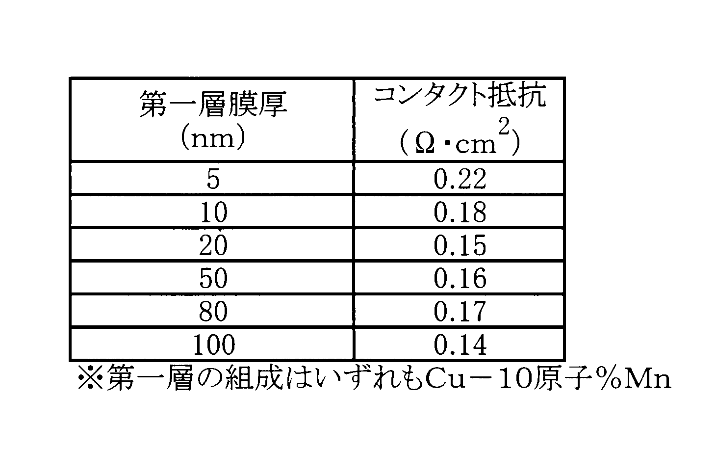
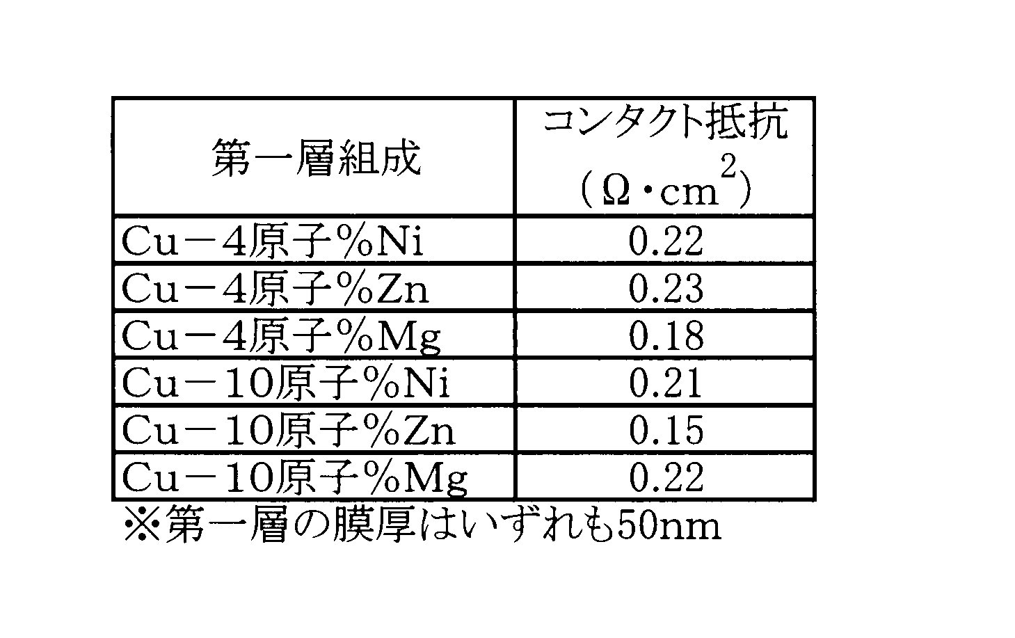
- Example 2 Measurement of contact resistance Cu alloy layers shown in Tables 1 to 3 (in these tables, only the composition / film thickness of the first layer is described, and the second layer is pure Cu), a semiconductor layer, In order to investigate the contact resistance, a TLM element was formed by the TLM method (Transfer Length Method).
- a low resistance amorphous silicon film (na-Si: H layer) doped with an impurity (P) having a thickness of about 200 nm was formed on a glass substrate by plasma CVD.
- an impurity P
- the RF power density applied to the plasma was 0.3 W / cm 2 for baking, the deposition temperature was 320 ° C., and the gas pressure was 67 Pa.
- a low-resistance amorphous silicon film doped with impurities (P) was continuously formed again without removing it from the CVD apparatus (film thickness: 10 nm).
- a Cu—X alloy was sputter-deposited on the conditions shown in Tables 1 to 3 (composition of the first layer, film thickness of the first layer), and a pure Cu film having a film thickness of 300 nm was further formed.
- the film formation temperature for sputtering was room temperature.
- a TLM evaluation element was created.
- a heat treatment was performed at 300 ° C. for 30 minutes to form a Cu—Si diffusion layer.
- FIG. 7A is a cross-sectional view schematically showing a wiring structure after the Cu—Si diffusion layer is formed as described above, and FIG. 7B is a top view thereof. In FIG. 7A, the Cu—Si diffusion layer is omitted.
- Table 1 also shows the results when pure Cu is used as the first layer for comparison.
- each of the examples in Tables 1 to 3 (except for pure Cu in Table 1) has a wiring structure that satisfies the requirements of the present invention, and the contact resistance with the semiconductor layer measured using a TLM evaluation element is 0.1 to 0. .3 ⁇ ⁇ cm 2 . That is, the contact resistance between the wiring structure of the present invention and the semiconductor layer is about the same as or lower than that of pure Cu, indicating a practical low contact resistance.
- the first layer shown in Table 2 satisfies the preferable relational expression defined by the present invention in terms of Mn content and the film thickness of the first layer, and keeps not only adhesion but also contact resistance with the semiconductor layer low. It has been.
- Table 3 shows an example in which Ni, Zn, and Mg are used as the X element, and low contact resistance is realized.
- Example 3 Measurement of electrical resistivity
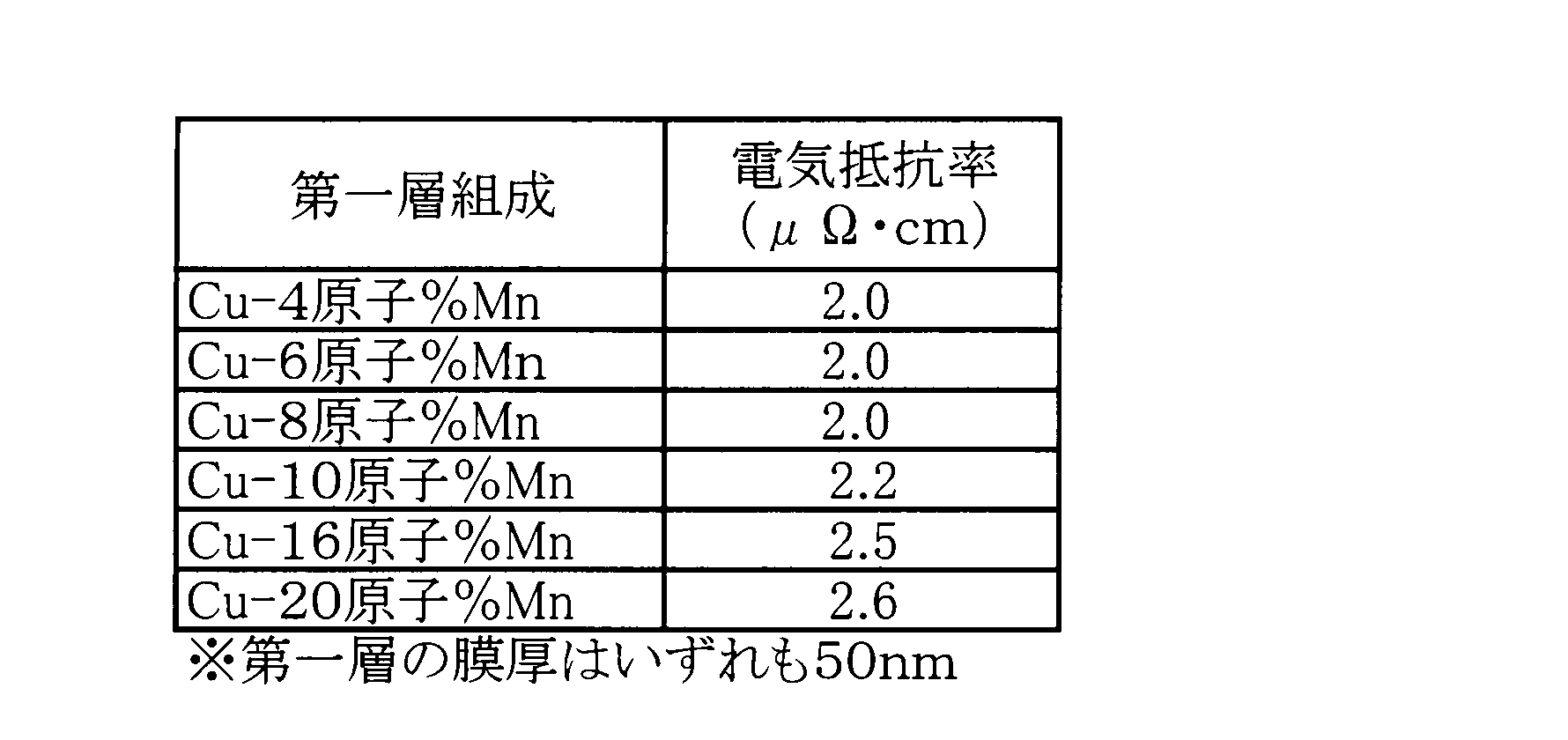
- the relationship between the film thickness of the first layer and the electrical resistivity of the entire Cu alloy layer (first layer + second layer), and the inclusion of the X element in the first layer The relationship between the amount and the electrical resistivity of the entire Cu alloy layer (first layer + second layer) was examined.
- a Cu—Mn alloy film was formed as the first layer under various conditions (first layer thickness, Mn content) shown in Tables 4 and 5. Furthermore, a pure Cu film was formed thereon (the film thickness of the entire Cu alloy layer was 300 nm).
- the substrate was heated and subjected to a heat treatment at 350 ° C. for 30 minutes, and the electric resistance after the heat treatment was measured at room temperature by a DC four-probe method.
- the electrical resistivity of the entire Cu alloy layer tends to increase as the film thickness of the first layer increases, and as shown in Table 5, the Mn content in the first layer There was a tendency that the electrical resistivity of the entire Cu alloy layer increased with the increase. However, in any of the examples shown in Tables 4 and 5, the electrical resistivity of the entire Cu alloy layer shows a practical low electrical resistivity.
- Example 4 Examination of the relationship between the thickness of the second semiconductor layer and the electrical resistivity In this example, the relationship between the thickness of the second semiconductor layer and the electrical resistivity of the entire Cu alloy layer (first layer + second layer) investigated.
- a low resistance amorphous silicon film (na-Si: H layer) doped with an impurity (P) having a thickness of about 200 nm was formed on a glass substrate by plasma CVD.
- an impurity P
- the RF power density applied to this plasma was about 0.3 W / cm 2
- the film formation temperature was 320 ° C.
- the gas pressure was 67 Pa.
- a low-resistance amorphous silicon film doped again with impurities (P) was continuously formed as a second semiconductor layer without being taken out from the CVD apparatus.
- the thickness of the second semiconductor layer at this time was set to 0 nm to 50 nm.
- a Cu-10 atomic% Mn film was formed thereon as a first layer, and a pure Cu film was formed thereon as a sputter film.
- the total film thickness of the Cu alloy layer was set to 300 nm.
- the film formation temperature of sputtering was room temperature.
- the same pattern as in Example 3 was processed by photolithography, wet etching, and dry etching.
- FIG. 10 shows that the electrical resistivity of the entire Cu alloy layer increases as the thickness of the second semiconductor layer increases.
- the electric resistance of the wiring film is desirably kept lower than the electric resistivity of 5.0 ⁇ cm when an existing technique such as an Al—Nd / Mo laminated structure is heat-treated at 300 ° C. for 30 minutes. From the above results, when the heat treatment is performed at 300 ° C. for 30 minutes, the thickness of the second semiconductor layer is preferably 45 nm or less. Further, the rate of increase in electrical resistance can be adjusted by adjusting the heat treatment temperature and time, but is generally preferably about 45 nm or less.
- Example 5 Measurement of TFT Characteristics
- the TFT characteristics when the wiring structure according to the present invention was adopted for the source / drain wiring were examined.
- a Cu alloy film was formed as a gate wiring on a glass substrate by DC magnetron sputtering.
- a gate insulating film SiN having a film thickness of about 200 nm was formed by plasma CVD.
- an a-Si semiconductor layer having a film thickness of about 200 nm is continuously formed without taking out from the CVD apparatus, and then a low-resistance amorphous silicon film doped with an impurity (P) (n + -a-Si layer) was deposited to 40 nm.
- P impurity
- the RF power density applied to this plasma was about 0.3 W / cm 2 , the film formation temperature was 320 ° C., and the gas pressure was 67 Pa.
- a low-resistance amorphous silicon film doped with impurities (P) again in the same plasma apparatus was formed as a second semiconductor layer.
- the thickness of the second semiconductor layer at this time was 5 nm.
- Cu-10 at% Mn was formed on the first layer as a source / drain wiring by a DC magnetron sputtering method, and a pure Cu film was formed thereon by sputtering, so that the film thickness of the entire Cu alloy layer was 300 nm.
- the substrate temperature for sputtering was room temperature.
- FIG. 11 shows the Id-Vg characteristics of the TFT formed by this process.
- the ratio of off-current to on-current is about 6 digits, and the source / drain wiring film has a conventional Cu / Mo laminated structure (a barrier such as Mo between the Cu-based alloy wiring film and the TFT semiconductor layer). It was found that the ratio of the off-current to the on-current of the TFT in the case of applying a laminated structure provided with a metal layer was comparable. Therefore, it was found that the TFT to which the present invention is applied operates without any problem.
- the present invention is a direct contact technology capable of directly contacting a Cu alloy layer with a semiconductor layer, and not only has excellent contact resistance between the Cu alloy layer and the semiconductor layer, but also has good productivity.
- it is possible to provide a technique with a further increased process margin. Specifically, it is difficult to be affected by variations in various process conditions (variation in equipment performance, instability, unexpected contamination, contamination that is difficult to control, etc.), and it is not necessary to manage extremely strict conditions. It is possible to provide technology that is not easily restricted.
- the first layer of the Cu alloy layer is Cu— containing X (X is at least one selected from the group consisting of Zn, Ni, Ti, Al, Mg, Ca, W, Nb and Mn) as an alloy component.
- the X alloy layer (first layer) and the second layer are pure Cu or a Cu alloy containing Cu as a main component and having a lower electrical resistivity than the first layer, the semiconductor While improving the adhesiveness with a layer and low contact resistance, the raise of the electrical resistivity as the whole Cu alloy layer can be suppressed.
Landscapes
- Thin Film Transistor (AREA)
- Internal Circuitry In Semiconductor Integrated Circuit Devices (AREA)
- Electrodes Of Semiconductors (AREA)
- Insulated Gate Type Field-Effect Transistor (AREA)
Abstract
Description
[1] 基板の上に、基板側から順に、半導体層と、Cu合金層とを備えた配線構造であって、
前記半導体層と前記Cu合金層との間に、基板側から順に、窒素、炭素、フッ素、及び酸素よりなる群から選択される少なくとも一種の元素を含有する(N、C、F、O)層と、CuおよびSiを含むCu-Si拡散層との積層構造を含んでおり、且つ、前記(N、C、F、O)層を構成する窒素、炭素、フッ素および酸素のいずれかの元素は前記半導体層のSiと結合しており、
前記Cu合金層は、基板側から順に、Zn、Ni、Ti、Al、Mg、Ca、W、NbおよびMnよりなる群から選択される少なくとも一種の合金成分Xを含有するCu-X合金層である第一層と、純Cu、またはCuを主成分とするCu合金であって前記第一層よりも電気抵抗率の低いCu合金からなる層である第二層、とを含む積層構造である配線構造。
[2] 前記Cu-X合金層である第一層におけるX含有量が0.5~20原子%である[1]に記載の配線構造。
[3] 前記Cu-X合金層である第一層の膜厚が5~150nmであり、Cu合金層全膜厚に対して50%以下である[1]または[2]に記載の配線構造。
[4] 前記Cu-X合金層である第一層の膜厚x(nm)と、Xの含有量y(原子%)が、下記(1)式の関係を満たす[1]~[3]のいずれか一つに記載の配線構造。
y≧-0.085x+8.0 ・・・(1)
[5] 前記Cu-Si拡散層は、前記(N、C、F、O)層、半導体層、および前記Cu合金層をこの順序で形成した後、熱履歴を加えることによって得られる[1]~[4]のいずれか一つに記載の配線構造。
[6] 前記半導体層は、水素化アモルファスシリコン、またはアモルファスシリコンである[1]~[5]のいずれか一つに記載の配線構造。
[7] [1]~[6]のいずれか一つに記載の配線構造を有する表示装置。
[8] [1]~[6]のいずれか一つに記載の配線構造を有する半導体装置。
本発明に係るTFTの第1の実施形態を図1Aに示す。図1Aは、TFT用基板の上に第1の半導体層を有し、その上に直接(N、C、F、O)層とCu-Si拡散層とからなる2層の積層構造を有しており、その上に直接Cu合金層(第一層と第二層を含む)が形成された構造を有している。図1Aの構造は、(N、C、F、O)層を形成した後、第2の半導体層、次いでCu合金層(積層構造)を形成し、その後に約150℃以上の熱履歴を加えることによって得られる。
第一層は、合金成分としてX(Xは、Zn、Ni、Ti、Al、Mg、Ca、W、NbおよびMnよりなる群から選択される少なくとも一種)を含有するCu-X合金層である。このような第一層とすることによってバリアメタル層を介在させなくても半導体層(Cu-Si拡散層に変化する半導体層も含む趣旨であり、よって第1の半導体層と第2の半導体層の両方を含む。以下、本発明におけるCu合金層と半導体層との密着性について述べる場合は同じ。)との密着性が向上できるとともに、半導体層との低接触抵抗を達成することができる。これらのX元素は、Cu金属には固溶するがCu酸化膜には固溶しない元素として選択したものである。これらの元素が固溶しているCu合金が成膜過程の熱処理によって酸化されると、上記元素は拡散して粒界や界面に濃化し、該濃化層によって半導体層との密着性が向上すると考えられる。またこれら元素は、Cuを用いた場合の有用性(Cu自体の低電気抵抗、および低接触抵抗)は何ら阻害することなく上記密着性を発揮できる。
y≧-0.085x+8.0 ・・・(1)
上記(1)式の関係を満たさない場合は、密着性が不十分となるおそれがある。密着性についていえば上記(1)式を満たす限り膜厚が厚いほど良いが、上記したように膜厚が厚くなりすぎるとCu合金層全体の電気抵抗が高くなるおそれがあるため、密着性と電気抵抗のバランスを考慮して膜厚を適切に制御することが好ましい。
本発明におけるCu合金層において、第二層は第一層の上(直上)に形成されており、純Cu、またはCuを主成分とするCu合金であって上記第一層よりも電気抵抗率の低いCu合金で構成されている。ここで、Cuを主成分とするとは、Cu合金中に含まれる元素の中で、Cuが最も多く含まれていることを意味する。Cu合金中のCuの含有量は、後述するように適用される合金元素によって異なるため一概には言えないが、例えば、60原子%以上(好ましくは70原子%)100原子%未満(好ましくは99.9原子%以下)であることが好ましい。このような第二層を設けることにより、Cu合金層全体の電気抵抗率を低く抑えることができる。ここで、第一層よりも電気抵抗率の低いCu合金とは、X元素を含むCu-X合金で構成されている第一層に比べて電気抵抗率が低くなるように合金元素の種類および/または含有量を適切に制御すれば良い。電気抵抗率が低い元素(おおむね、純Cu合金並みに低い元素)は、文献に記載の数値などを参照し、公知の元素から容易に選択することができる。ただし、電気抵抗率が高い元素であっても含有量を少なくすれば(おおむね、0.05~1原子%程度)電気抵抗率を低減できるため、第二層に適用可能な合金元素は、必ずしも電気抵抗率が低い元素に限定されない。具体的には、例えばCu-0.5原子%Ni、Cu-0.5原子%Zn、Cu-0.3原子%Mnなどが好ましく用いられる。また、第二層に適用可能な合金としては、酸素ガスや窒素ガスなどのガス成分を含むものであってもよく、例えばCu-OやCu-Nなどを用いることができる。
本発明に係るTFTの第2の実施形態は、上述した第1の実施形態における2層の積層構造を構成する(N、C、F、O)層と、TFT用基板の間に、第1の半導体層、(N、C、F、O)層、第1の半導体層を有している例である。詳細には、図2に示すように、TFT用基板の上に第1の半導体層、(N、C、F、O)層、第1の半導体層を有し、その上に直接、(N、C、F、O)層とCu-Si拡散層とからなる2層の積層構造を有しており、その上に直接、Cu合金層が形成された構造を有している。
本発明に係るMOSFETの第1の実施形態を図4に示す。図4は、単結晶Siの上に直接、(N、C、F、O)層とCu-Si拡散層とからなる2層の積層構造を有しており、その上に直接、Cu合金層が形成された構造を有している。このような構造は図5に示す工程により形成される。すなわち、イオン注入法などによりN、C、F、Oのうち例えば窒素を単結晶Si基板中に打ち込む。このとき、注入された窒素はある深さ(飛程と呼ばれる)を中心にほぼガウス分布の深さ方向分布を有する。注入された窒素のダメージによりSiの一部はアモルファス化する。次にCu合金層をスパッタとメッキにより成膜し、その後アニールなどの熱処理を施すことでCu合金層(第一層と第二層を含む)/Cu-Si拡散層/窒素含有層/単結晶Siの構造が形成される。
実施例1では以下の要領でCu合金層の第一層の組成を変化させた試料を作成し、Cu合金層と半導体層との密着性を評価した。
表1~3に示すCu合金層(これらの表には第一層の組成/膜厚のみを記載しており、第2層は純Cuである)と半導体層とのコンタクト抵抗を調べるため、TLM法(Transfer Length Method)によりTLM素子を形成した。
ρc=Rc×LT×Z
上式中、Zは図7(b)に示すように電極幅を示す。

本実施例では、第一層の膜厚とCu合金層全体(第一層+第二層)の電気抵抗率の関係、および第一層中のX元素の含有量とCu合金層全体(第一層+第二層)の電気抵抗率の関係を検討した。

本実施例では第2の半導体層の厚みとCu合金層全体(第一層+第二層)の電気抵抗率の関係を検討した。
本実施例では、本発明に係る配線構造をソース/ドレイン配線に採用した際のTFT特性について検討した。
本出願は、2010年4月2日出願の日本特許出願(特願2010-086485)に基づくものであり、その内容はここに参照として取り込まれる。
Claims (34)
- 基板の上に、基板側から順に、半導体層と、Cu合金層とを備えた配線構造であって、
前記半導体層と前記Cu合金層との間に、基板側から順に、窒素、炭素、フッ素、及び酸素よりなる群から選択される少なくとも一種の元素を含有する(N、C、F、O)層と、CuおよびSiを含むCu-Si拡散層との積層構造を含んでおり、且つ、前記(N、C、F、O)層を構成する窒素、炭素、フッ素および酸素のいずれかの元素は前記半導体層のSiと結合しており、
前記Cu合金層は、基板側から順に、Zn、Ni、Ti、Al、Mg、Ca、W、NbおよびMnよりなる群から選択される少なくとも一種の合金成分Xを含有するCu-X合金層である第一層と、純Cu、またはCuを主成分とするCu合金であって前記第一層よりも電気抵抗率の低いCu合金からなる層である第二層、とを含む積層構造である配線構造。 - 前記Cu-X合金層である第一層におけるX含有量が0.5~20原子%である請求項1に記載の配線構造。
- 前記Cu-X合金層である第一層の膜厚が5~150nmであり、Cu合金層全膜厚に対して50%以下である請求項1に記載の配線構造。
- 前記Cu-X合金層である第一層の膜厚が5~150nmであり、Cu合金層全膜厚に対して50%以下である請求項2に記載の配線構造。
- 前記Cu-X合金層である第一層の膜厚x(nm)と、Xの含有量y(原子%)が、下記(1)式の関係を満たす請求項1項に記載の配線構造。
y≧-0.085x+8.0 ・・・(1) - 前記Cu-X合金層である第一層の膜厚x(nm)と、Xの含有量y(原子%)が、下記(1)式の関係を満たす請求項2に記載の配線構造。
y≧-0.085x+8.0 ・・・(1) - 前記Cu-X合金層である第一層の膜厚x(nm)と、Xの含有量y(原子%)が、下記(1)式の関係を満たす請求項3に記載の配線構造。
y≧-0.085x+8.0 ・・・(1) - 前記Cu-X合金層である第一層の膜厚x(nm)と、Xの含有量y(原子%)が、下記(1)式の関係を満たす請求項4に記載の配線構造。
y≧-0.085x+8.0 ・・・(1) - 前記Cu-Si拡散層は、前記(N、C、F、O)層、半導体層、および前記Cu合金層をこの順序で形成した後、熱履歴を加えることによって得られる請求項1記載の配線構造。
- 前記Cu-Si拡散層は、前記(N、C、F、O)層、半導体層、および前記Cu合金層をこの順序で形成した後、熱履歴を加えることによって得られる請求項2に記載の配線構造。
- 前記Cu-Si拡散層は、前記(N、C、F、O)層、半導体層、および前記Cu合金層をこの順序で形成した後、熱履歴を加えることによって得られる請求項3に記載の配線構造。
- 前記Cu-Si拡散層は、前記(N、C、F、O)層、半導体層、および前記Cu合金層をこの順序で形成した後、熱履歴を加えることによって得られる請求項4に記載の配線構造。
- 前記Cu-Si拡散層は、前記(N、C、F、O)層、半導体層、および前記Cu合金層をこの順序で形成した後、熱履歴を加えることによって得られる請求項5に記載の配線構造。
- 前記Cu-Si拡散層は、前記(N、C、F、O)層、半導体層、および前記Cu合金層をこの順序で形成した後、熱履歴を加えることによって得られる請求項6に記載の配線構造。
- 前記Cu-Si拡散層は、前記(N、C、F、O)層、半導体層、および前記Cu合金層をこの順序で形成した後、熱履歴を加えることによって得られる請求項7に記載の配線構造。
- 前記Cu-Si拡散層は、前記(N、C、F、O)層、半導体層、および前記Cu合金層をこの順序で形成した後、熱履歴を加えることによって得られる請求項8に記載の配線構造。
- 前記半導体層は、水素化アモルファスシリコン、またはアモルファスシリコンである請求項1に記載の配線構造。
- 前記半導体層は、水素化アモルファスシリコン、またはアモルファスシリコンである請求項2に記載の配線構造。
- 前記半導体層は、水素化アモルファスシリコン、またはアモルファスシリコンである請求項3に記載の配線構造。
- 前記半導体層は、水素化アモルファスシリコン、またはアモルファスシリコンである請求項4に記載の配線構造。
- 前記半導体層は、水素化アモルファスシリコン、またはアモルファスシリコンである請求項5に記載の配線構造。
- 前記半導体層は、水素化アモルファスシリコン、またはアモルファスシリコンである請求項6に記載の配線構造。
- 前記半導体層は、水素化アモルファスシリコン、またはアモルファスシリコンである請求項7に記載の配線構造。
- 前記半導体層は、水素化アモルファスシリコン、またはアモルファスシリコンである請求項8に記載の配線構造。
- 前記半導体層は、水素化アモルファスシリコン、またはアモルファスシリコンである請求項9に記載の配線構造。
- 前記半導体層は、水素化アモルファスシリコン、またはアモルファスシリコンである請求項10に記載の配線構造。
- 前記半導体層は、水素化アモルファスシリコン、またはアモルファスシリコンである請求項11に記載の配線構造。
- 前記半導体層は、水素化アモルファスシリコン、またはアモルファスシリコンである請求項12に記載の配線構造。
- 前記半導体層は、水素化アモルファスシリコン、またはアモルファスシリコンである請求項13に記載の配線構造。
- 前記半導体層は、水素化アモルファスシリコン、またはアモルファスシリコンである請求項14に記載の配線構造。
- 前記半導体層は、水素化アモルファスシリコン、またはアモルファスシリコンである請求項15に記載の配線構造。
- 前記半導体層は、水素化アモルファスシリコン、またはアモルファスシリコンである請求項16に記載の配線構造。
- 請求項1~32のいずれか一項に記載の配線構造を有する表示装置。
- 請求項1~32のいずれか一項に記載の配線構造を有する半導体装置。
Priority Applications (3)
| Application Number | Priority Date | Filing Date | Title |
|---|---|---|---|
| CN201180016158.2A CN102822945B (zh) | 2010-04-02 | 2011-03-30 | 配线构造、显示装置和半导体装置 |
| KR1020127025711A KR20120134137A (ko) | 2010-04-02 | 2011-03-30 | 배선 구조, 표시 장치 및 반도체 장치 |
| US13/639,028 US8598580B2 (en) | 2010-04-02 | 2011-03-30 | Wiring structure, display apparatus, and semiconductor device |
Applications Claiming Priority (2)
| Application Number | Priority Date | Filing Date | Title |
|---|---|---|---|
| JP2010086485A JP2011222567A (ja) | 2010-04-02 | 2010-04-02 | 配線構造、表示装置、および半導体装置 |
| JP2010-086485 | 2010-04-02 |
Publications (1)
| Publication Number | Publication Date |
|---|---|
| WO2011125802A1 true WO2011125802A1 (ja) | 2011-10-13 |
Family
ID=44762741
Family Applications (1)
| Application Number | Title | Priority Date | Filing Date |
|---|---|---|---|
| PCT/JP2011/058141 Ceased WO2011125802A1 (ja) | 2010-04-02 | 2011-03-30 | 配線構造、表示装置、および半導体装置 |
Country Status (6)
| Country | Link |
|---|---|
| US (1) | US8598580B2 (ja) |
| JP (1) | JP2011222567A (ja) |
| KR (1) | KR20120134137A (ja) |
| CN (1) | CN102822945B (ja) |
| TW (1) | TWI449127B (ja) |
| WO (1) | WO2011125802A1 (ja) |
Families Citing this family (4)
| Publication number | Priority date | Publication date | Assignee | Title |
|---|---|---|---|---|
| JP5171990B2 (ja) | 2011-05-13 | 2013-03-27 | 株式会社神戸製鋼所 | Cu合金膜および表示装置 |
| CN104882488B (zh) * | 2015-06-15 | 2018-03-20 | 合肥鑫晟光电科技有限公司 | 薄膜晶体管、阵列基板及其制作方法、显示装置 |
| US9748281B1 (en) * | 2016-09-15 | 2017-08-29 | International Business Machines Corporation | Integrated gate driver |
| KR20240159006A (ko) * | 2018-03-28 | 2024-11-05 | 다이니폰 인사츠 가부시키가이샤 | 배선 기판 |
Citations (3)
| Publication number | Priority date | Publication date | Assignee | Title |
|---|---|---|---|---|
| JP2008124450A (ja) * | 2006-10-19 | 2008-05-29 | Ulvac Japan Ltd | ターゲット、成膜方法、薄膜トランジスタ、薄膜トランジスタ付パネル、薄膜トランジスタの製造方法、及び薄膜トランジスタ付パネルの製造方法 |
| WO2009131035A1 (ja) * | 2008-04-25 | 2009-10-29 | 株式会社アルバック | 薄膜トランジスタの製造方法、薄膜トランジスタ |
| WO2010001998A1 (ja) * | 2008-07-03 | 2010-01-07 | 株式会社神戸製鋼所 | 配線構造、薄膜トランジスタ基板およびその製造方法、並びに表示装置 |
Family Cites Families (12)
| Publication number | Priority date | Publication date | Assignee | Title |
|---|---|---|---|---|
| JP2733006B2 (ja) | 1993-07-27 | 1998-03-30 | 株式会社神戸製鋼所 | 半導体用電極及びその製造方法並びに半導体用電極膜形成用スパッタリングターゲット |
| JP3940385B2 (ja) | 2002-12-19 | 2007-07-04 | 株式会社神戸製鋼所 | 表示デバイスおよびその製法 |
| KR100904524B1 (ko) | 2002-12-31 | 2009-06-25 | 엘지디스플레이 주식회사 | 액정표시장치용 어레이기판 제조방법 |
| JP2005303003A (ja) | 2004-04-12 | 2005-10-27 | Kobe Steel Ltd | 表示デバイスおよびその製法 |
| JP4541787B2 (ja) | 2004-07-06 | 2010-09-08 | 株式会社神戸製鋼所 | 表示デバイス |
| JP4330517B2 (ja) | 2004-11-02 | 2009-09-16 | 株式会社神戸製鋼所 | Cu合金薄膜およびCu合金スパッタリングターゲット並びにフラットパネルディスプレイ |
| JP4117001B2 (ja) | 2005-02-17 | 2008-07-09 | 株式会社神戸製鋼所 | 薄膜トランジスタ基板、表示デバイス、および表示デバイス用のスパッタリングターゲット |
| US7683370B2 (en) | 2005-08-17 | 2010-03-23 | Kobe Steel, Ltd. | Source/drain electrodes, transistor substrates and manufacture methods, thereof, and display devices |
| US7411298B2 (en) | 2005-08-17 | 2008-08-12 | Kabushiki Kaisha Kobe Seiko Sho (Kobe Steel, Ltd.) | Source/drain electrodes, thin-film transistor substrates, manufacture methods thereof, and display devices |
| US7781767B2 (en) | 2006-05-31 | 2010-08-24 | Kobe Steel, Ltd. | Thin film transistor substrate and display device |
| JP5214858B2 (ja) | 2006-06-22 | 2013-06-19 | 三菱電機株式会社 | Tftアレイ基板及びその製造方法 |
| JP2008098611A (ja) * | 2006-09-15 | 2008-04-24 | Kobe Steel Ltd | 表示装置 |
-
2010
- 2010-04-02 JP JP2010086485A patent/JP2011222567A/ja active Pending
-
2011
- 2011-03-30 US US13/639,028 patent/US8598580B2/en not_active Expired - Fee Related
- 2011-03-30 CN CN201180016158.2A patent/CN102822945B/zh not_active Expired - Fee Related
- 2011-03-30 WO PCT/JP2011/058141 patent/WO2011125802A1/ja not_active Ceased
- 2011-03-30 KR KR1020127025711A patent/KR20120134137A/ko not_active Ceased
- 2011-04-01 TW TW100111651A patent/TWI449127B/zh not_active IP Right Cessation
Patent Citations (3)
| Publication number | Priority date | Publication date | Assignee | Title |
|---|---|---|---|---|
| JP2008124450A (ja) * | 2006-10-19 | 2008-05-29 | Ulvac Japan Ltd | ターゲット、成膜方法、薄膜トランジスタ、薄膜トランジスタ付パネル、薄膜トランジスタの製造方法、及び薄膜トランジスタ付パネルの製造方法 |
| WO2009131035A1 (ja) * | 2008-04-25 | 2009-10-29 | 株式会社アルバック | 薄膜トランジスタの製造方法、薄膜トランジスタ |
| WO2010001998A1 (ja) * | 2008-07-03 | 2010-01-07 | 株式会社神戸製鋼所 | 配線構造、薄膜トランジスタ基板およびその製造方法、並びに表示装置 |
Also Published As
| Publication number | Publication date |
|---|---|
| US8598580B2 (en) | 2013-12-03 |
| CN102822945B (zh) | 2016-04-27 |
| CN102822945A (zh) | 2012-12-12 |
| KR20120134137A (ko) | 2012-12-11 |
| TW201214623A (en) | 2012-04-01 |
| TWI449127B (zh) | 2014-08-11 |
| US20130026470A1 (en) | 2013-01-31 |
| JP2011222567A (ja) | 2011-11-04 |
Similar Documents
| Publication | Publication Date | Title |
|---|---|---|
| JP5584436B2 (ja) | 薄膜トランジスタ基板の製造方法 | |
| JP5475260B2 (ja) | 配線構造、薄膜トランジスタ基板およびその製造方法、並びに表示装置 | |
| CN103003860B (zh) | 显示装置用Cu合金膜和显示装置 | |
| TWI496197B (zh) | Wiring structure | |
| CN101330102A (zh) | 薄膜晶体管基板和显示器件 | |
| WO2012043806A1 (ja) | 配線構造および表示装置 | |
| CN102804352A (zh) | 布线层结构及其制造方法 | |
| JP5580619B2 (ja) | 薄膜トランジスタ基板および表示デバイス | |
| JP5685125B2 (ja) | 配線構造、表示装置、および半導体装置 | |
| CN102822945B (zh) | 配线构造、显示装置和半导体装置 | |
| JP2008010801A (ja) | ソース−ドレイン電極、薄膜トランジスタ基板およびその製造方法、並びに表示デバイス | |
| JP2012109465A (ja) | 表示装置用金属配線膜 | |
| JP2009016862A (ja) | ソース−ドレイン電極、薄膜トランジスタ基板およびその製造方法、並びに表示デバイス | |
| WO2018181296A1 (ja) | チャネルエッチ型薄膜トランジスタの製造方法 |
Legal Events
| Date | Code | Title | Description |
|---|---|---|---|
| WWE | Wipo information: entry into national phase |
Ref document number: 201180016158.2 Country of ref document: CN |
|
| 121 | Ep: the epo has been informed by wipo that ep was designated in this application |
Ref document number: 11765702 Country of ref document: EP Kind code of ref document: A1 |
|
| ENP | Entry into the national phase |
Ref document number: 20127025711 Country of ref document: KR Kind code of ref document: A |
|
| NENP | Non-entry into the national phase |
Ref country code: DE |
|
| WWE | Wipo information: entry into national phase |
Ref document number: 13639028 Country of ref document: US |
|
| 122 | Ep: pct application non-entry in european phase |
Ref document number: 11765702 Country of ref document: EP Kind code of ref document: A1 |