WO2011125707A1 - アンテナ装置及びこれを用いた無線通信機 - Google Patents
アンテナ装置及びこれを用いた無線通信機 Download PDFInfo
- Publication number
- WO2011125707A1 WO2011125707A1 PCT/JP2011/057961 JP2011057961W WO2011125707A1 WO 2011125707 A1 WO2011125707 A1 WO 2011125707A1 JP 2011057961 W JP2011057961 W JP 2011057961W WO 2011125707 A1 WO2011125707 A1 WO 2011125707A1
- Authority
- WO
- WIPO (PCT)
- Prior art keywords
- antenna
- circuit board
- antenna device
- printed circuit
- edge
- Prior art date
- Legal status (The legal status is an assumption and is not a legal conclusion. Google has not performed a legal analysis and makes no representation as to the accuracy of the status listed.)
- Ceased
Links
Images










Classifications
-
- H—ELECTRICITY
- H01—ELECTRIC ELEMENTS
- H01Q—ANTENNAS, i.e. RADIO AERIALS
- H01Q1/00—Details of, or arrangements associated with, antennas
- H01Q1/36—Structural form of radiating elements, e.g. cone, spiral, umbrella; Particular materials used therewith
- H01Q1/38—Structural form of radiating elements, e.g. cone, spiral, umbrella; Particular materials used therewith formed by a conductive layer on an insulating support
-
- H—ELECTRICITY
- H05—ELECTRIC TECHNIQUES NOT OTHERWISE PROVIDED FOR
- H05K—PRINTED CIRCUITS; CASINGS OR CONSTRUCTIONAL DETAILS OF ELECTRIC APPARATUS; MANUFACTURE OF ASSEMBLAGES OF ELECTRICAL COMPONENTS
- H05K1/00—Printed circuits
- H05K1/02—Details
- H05K1/0213—Electrical arrangements not otherwise provided for
- H05K1/0237—High frequency adaptations
- H05K1/0243—Printed circuits associated with mounted high frequency components
-
- H—ELECTRICITY
- H05—ELECTRIC TECHNIQUES NOT OTHERWISE PROVIDED FOR
- H05K—PRINTED CIRCUITS; CASINGS OR CONSTRUCTIONAL DETAILS OF ELECTRIC APPARATUS; MANUFACTURE OF ASSEMBLAGES OF ELECTRICAL COMPONENTS
- H05K2201/00—Indexing scheme relating to printed circuits covered by H05K1/00
- H05K2201/10—Details of components or other objects attached to or integrated in a printed circuit board
- H05K2201/10007—Types of components
- H05K2201/10098—Components for radio transmission, e.g. radio frequency identification [RFID] tag, printed or non-printed antennas
Definitions
- the present invention relates to an antenna device and a wireless communication device using the antenna device, and more particularly to a technique for adjusting antenna characteristics.
- Bluetooth (registered trademark) and GPS chip antennas are built in small mobile terminals such as mobile phones.
- This type of chip antenna is required to be small in size and to be easily adjusted in resonance frequency and impedance matching.
- the resonant frequency and input impedance of a chip antenna change due to the effects of the structure of the printed circuit board, various electronic components mounted around it, and the housing, and it is necessary to adjust the resonant frequency and input impedance for each model. It is.
- Patent Document 1 As a method for adjusting the resonance frequency and the input impedance, for example, as described in Patent Document 1, a method using a chip component such as a chip capacitor or a chip inductor is known. Patent Documents 2 and 3 propose a frequency variable circuit using a varicap diode as a method for adjusting the resonance frequency.
- the present invention has been completed in view of the above problems, and a main object thereof is to realize an antenna device that can easily adjust the resonance frequency of the antenna and can be easily manufactured. Moreover, the objective of this invention is providing the radio
- an antenna device includes an antenna element and a printed board on which the antenna element is mounted.
- the antenna element includes a base made of a dielectric and at least one surface of the base.
- the printed circuit board includes a substantially rectangular ground clearance region in which one side is in contact with an edge of the printed circuit board and the other three sides are surrounded by an edge line of a ground pattern, and the ground
- the wireless communication device includes a communication circuit unit and the antenna device according to the present invention, and the communication circuit unit is mounted on the printed board.
- the edge line of the ground pattern is opposite to the first edge line orthogonal to the edge of the printed circuit board, the second edge line facing the edge of the printed circuit board, and the first edge line.
- the distance from the frequency adjustment element to the second edge line is shorter than the distance from the frequency adjustment element to the antenna mounting region.
- the position of the frequency adjusting element in the ground clearance region is biased toward the first edge line side or the third edge line side. According to this configuration, the rate of change of the resonance frequency with respect to the change of the frequency adjustment element can be made moderate as compared with the case where the frequency adjustment element is provided in the center in the width direction within the ground clearance region.
- one end and the other end of the frequency adjusting element are respectively connected to any of the first to third edge lines. According to this configuration, the rate of change of the resonance frequency with respect to the change of the frequency adjusting element can be made slower than when the frequency adjusting element is grounded via the terminal electrode.
- one end of the frequency adjustment element is connected to the first edge line via a first wiring pattern, and the other end of the frequency adjustment element is connected to the first edge line via a second wiring pattern. It is preferable to be connected to the second edge line. According to this configuration, since the connection pattern of the frequency adjusting elements is L-shaped, the change rate of the resonance frequency can be further reduced.
- the antenna device further includes first and second electrode patterns sandwiched between the bottom surface of the base and the printed board, the first electrode pattern being connected to the ground pattern,
- the electrode pattern is preferably connected to a power supply line.
- the first and second electrode patterns may be terminal electrodes on the antenna element side, land patterns on the printed circuit board side, or both of them. More preferably, it includes a terminal electrode on the element side. It is possible to omit the electrode pattern on the bottom surface of the base of the antenna element and form the electrode pattern only on the printed circuit board. However, if the first and second terminal electrodes are formed on the bottom of the base, It is possible to reduce the characteristic variation due to the positional deviation of the substrate placed on the substrate.
- the printed circuit board further includes first and second lands provided in the antenna mounting region corresponding to the first and second terminal electrodes, and the first terminal electrode It is preferable that the first land is connected to the ground pattern, and the second terminal electrode is connected to the power supply line on the printed circuit board via the second land.
- the antenna element can be solder-mounted, and the first land and the first terminal electrode, and the second terminal electrode and the feed line can be reliably connected.
- the antenna element further includes a third terminal electrode formed on a bottom surface of the base, and the printed circuit board is provided in the antenna mounting area corresponding to the third terminal electrode.
- a third land is further provided, and the third terminal electrode is connected to the ground pattern through the third land.
- at least one of the third terminal electrode and the third land has an L shape with an open end (tip) facing the edge side of the printed circuit board.
- the conductor pattern formed on the surface of the base of the antenna element is preferably symmetrical with respect to a center line extending in the longitudinal direction of the base. According to this configuration, even if the orientation of the antenna element is rotated 180 degrees with respect to the axis (Z axis) perpendicular to the upper and lower surfaces of the base, the shape of the conductor pattern of the antenna element viewed from the edge side of the printed circuit board is substantially Therefore, the antenna characteristics do not change greatly depending on the orientation of the antenna element. Therefore, antenna design can be facilitated.
- the present invention it is possible to provide an antenna device in which fine adjustment of the resonance frequency is easy even when a commercially available chip component is used.
- FIG. 1 is a schematic perspective view showing a configuration of an antenna device 100 according to the first embodiment of the present invention.
- FIG. 2 is a development view of the antenna element 10.
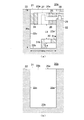
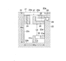
- 3A is a schematic plan view showing a pattern layout of the front surface 20a of the printed circuit board 20 on which the antenna element 10 is mounted
- FIG. 3B is a schematic view of the back surface 20b of the printed circuit board 20 on which the antenna element 10 is mounted. It is a schematic plan view showing a pattern layout.
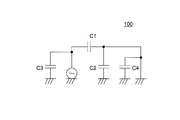
- FIG. 4 is an equivalent circuit diagram of the antenna device 100.
- FIG. 5 is a schematic perspective view showing the configuration of the antenna device 100A according to the second embodiment of the present invention.
- FIG. 6 is a schematic perspective view showing the configuration of an antenna device 200A according to the third embodiment of the present invention.
- FIG. 7 is a schematic perspective view showing the configuration of an antenna device 200B according to the fourth embodiment of the present invention.
- FIG. 8 is a schematic perspective view showing the configuration of an antenna device 300A according to the fifth embodiment of the present invention.
- FIG. 9 is a schematic perspective view showing the configuration of an antenna device 300B according to the sixth embodiment of the present invention.
- FIG. 10 is a schematic perspective view showing the configuration of an antenna device 400A according to the seventh embodiment of the present invention.
- FIG. 11 is a schematic perspective view showing the configuration of an antenna device 400B according to the seventh embodiment of the present invention.
- FIG. 12 is a schematic perspective view showing the configuration of an antenna device 500A according to the eighth embodiment of the present invention.
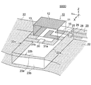
- FIG. 13 is a schematic perspective view showing the configuration of an antenna device 500B according to the ninth embodiment of the present invention.
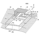
- FIG. 14 is a schematic perspective view showing the configuration of an antenna device 500C according to the tenth embodiment of the present invention.
- FIG. 15 is a schematic perspective view showing the configuration of an antenna device 500D according to the eleventh embodiment of the present invention.
- FIG. 16 is a schematic perspective view showing the configuration of the antenna device 600 according to the twelfth embodiment of the present invention.
- FIG. 17 is a graph showing frequency characteristics of the antenna device.
- FIG. 18 is a graph showing the frequency characteristics of the antenna device.
- FIG. 19 is a schematic perspective view showing the configuration of the antenna device 700 according to the thirteenth embodiment of the present invention.
- FIG. 20 is a development view of the antenna element 10.
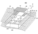
- FIG. 21 is a schematic perspective view showing the configuration of the antenna device 800 according to the fourteenth embodiment of the present invention.
- FIG. 22 is a development view of the antenna element 10.
- FIG. 23 is a schematic plan view showing a modification of the land pattern, which is the configuration of the antenna apparatus according to the fifteenth embodiment of the present invention.
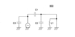
- FIG. 24 is an equivalent circuit diagram of an antenna apparatus 900 according to the sixteenth embodiment of the present invention.
- FIG. 25 is a graph showing frequency characteristics of the antenna device 900 according to the sixteenth embodiment of the present invention.
- FIG. 26 is a block diagram showing an example of the configuration of a wireless communication device using the antenna device according to the present invention.
- FIG. 1 is a schematic perspective view showing a configuration of an antenna device 100 according to a first embodiment of the present invention.
- FIG. 2 is a development view of the antenna element 10.
- the antenna device 100 includes an antenna element 10 and a printed board 20 on which the antenna element 10 is mounted.
- the antenna element 10 includes a base 11 made of a dielectric and a plurality of conductor patterns formed on the base 11.
- the base 11 has a rectangular parallelepiped shape with the Y direction as the longitudinal direction.
- the upper surface 11a, the bottom surface 11b, and the two side surfaces 11c and 11d of the base body 11 are surfaces parallel to the Y direction
- the side surfaces 11e and 11f are surfaces orthogonal to the Y direction
- the bottom surface 11b is mounted on the printed circuit board 20.
- the vertical direction of the antenna element 10 is defined with the surface of the printed circuit board 20 as a reference plane.
- the size of the substrate 11 is preferably as small as possible within a range in which a desired radiation efficiency can be ensured, and for example, a substrate having a size of 2.0 ⁇ 1.25 ⁇ 0.8 (mm) can be used.
- the material of the substrate 11 is not particularly limited, but a Ba—Nd—Ti-based material (relative permittivity of 80 to 120), an Nd—Al—Ca—Ti based material (relative permittivity of 43 to 46), Li—Al—Sr—Ti (relative permittivity 38 to 41), Ba—Ti based material (relative permittivity 34 to 36), Ba—Mg—W based material (relative permittivity 20 to 22), Mg—Ca— Ti-based materials (relative permittivity 19 to 21), sapphire (relative permittivity 9 to 10), alumina ceramics (relative permittivity 9 to 10), cordierite ceramics (relative permittivity 4 to 6), etc. can be used.
- the relative permittivity ⁇ r the greater the wavelength shortening effect is obtained, so that the length of the radiating conductor can be shortened, but the radiation efficiency is lowered, so that the relative permittivity ⁇ r is necessarily large. Rather, there is an appropriate value. Therefore, for example, when the target frequency is 2.4 GHz, it is preferable to use a material having a relative dielectric constant ⁇ r of about 5 to 100. According to this, it is possible to reduce the size of the base while ensuring sufficient radiation efficiency.
- Preferred examples of the material having a relative dielectric constant ⁇ r of about 5 to 100 include Mg—Ca—Ti based dielectric ceramics. As the Mg—Ca—Ti dielectric ceramic, it is particularly preferable to use an Mg—Ca—Ti dielectric ceramic containing TiO 2 , MgO, CaO, MnO, and SiO 2 .
- the conductor pattern of the antenna element 10 includes an upper surface conductor pattern 12 formed on the upper surface 11 a of the base body 11, a side conductor pattern 13 formed on the side surface 11 e of the base body 11, and a bottom surface 11 b of the base body 11.
- the first to third terminal electrodes 14 to 16 are formed.
- These conductor patterns can be formed by applying an electrode paste material by a method such as screen printing or transfer and then baking under a predetermined temperature condition.
- the electrode paste material silver, silver-palladium, silver-platinum, copper or the like can be used.
- the conductor pattern can also be formed by plating or sputtering.
- the upper surface conductor pattern 12 is a portion that contributes most to radio wave radiation, and is formed on the entire upper surface 11a of the base 11. Although not necessarily formed on the entire surface, the radiation efficiency can be increased as the area of the upper conductor pattern 12 is larger.
- One end of the upper surface conductor pattern 12 in the longitudinal direction is an open end, but is substantially capacitively coupled to the second and third terminal electrodes 15 and 16.
- the other end in the longitudinal direction of the top conductor pattern 12 is connected to the first terminal electrode 14 via the side conductor pattern 13, and the top conductor pattern 12, the side conductor pattern 13, and the first terminal electrode 14 are It constitutes one continuous radiating conductor.
- the radiation conductor is formed over a plurality of surfaces of the base body 11, a desired electrical length can be ensured even if the base body 11 itself is downsized.
- the first to third terminal electrodes 14 to 16 are electrodes for electrically and mechanically connecting the antenna element 10 to the printed circuit board 20.
- the first terminal electrode 14 is a ground electrode connected to the ground pattern 22 via the land 24 on the printed circuit board 20.
- the second terminal electrode 15 is a power supply electrode connected to the power supply line 28 via the land 25 on the printed circuit board 20, and the third terminal electrode 16 is connected to the land 26 on the printed circuit board 20.
- the first terminal electrode 14 is formed on one end side in the Y direction of the bottom surface 11 b and is connected to the lower end of the side conductor pattern 13.
- the second and third terminal electrodes 15 and 16 are formed on the other end side in the Y direction of the bottom surface 11b.
- the first terminal electrode 14 is formed over the entire width direction of the bottom surface 11b, and the terminal electrodes 15 and 16 are formed in the width direction (X direction) of the bottom surface 11b with a predetermined interval therebetween. That is, the width of the terminal electrodes 15 and 16 is less than 1 ⁇ 2 of the width of the bottom surface 11b.
- the gap between the upper surface conductor pattern 12 and the second terminal electrode 15 constitutes a capacitance C1, and the upper surface conductor pattern 12 is connected to the feeder line 28 via the capacitance C1.
- the gap between the upper surface conductor pattern 12 and the third terminal electrode 16 forms a capacitance C2, and the upper surface conductor pattern 12 is connected to the ground pattern 22 via the capacitance C2.
- the third terminal electrode 16 is L-shaped, and one end (open end) closer to the first terminal electrode 14 is bent at a right angle and extends in a direction approaching the second terminal electrode 15. Yes.
- the open end of the third terminal electrode 16 faces the edge side of the printed circuit board 20, so that electromagnetic coupling with the ground pattern can be weakened. , Radiation efficiency can be improved. Further, since the third terminal electrode 16 has a larger area than the second terminal electrode 15, the capacitance C2 can be made larger than the capacitance C1, and an appropriate capacitance is set in accordance with its function. be able to.
- FIG. 3 is a schematic plan view showing a pattern layout on the printed circuit board 20 on which the antenna element 10 is mounted.
- FIG. 3A is a layout of the front surface 20a of the printed circuit board 20
- FIG. 3B is a layout of the back surface 20b of the printed circuit board. It is.
- (b) shows the layout of the back surface 20b transparently from the front surface 20a side.
- the printed circuit board 20 is a circuit board on which a communication circuit unit for configuring a wireless communication device is mounted.
- the printed circuit board 20 includes an insulating substrate 21 and conductor patterns formed on the front and back surfaces of the insulating substrate 21. have.
- the surface 20 a of the printed circuit board 20 is provided with a ground clearance region 23 a in which one side is in contact with the edge 20 e of the printed circuit board 20 and the other three sides are defined by the ground pattern 22.
- the ground clearance area 23a is a mounting component, a conductor pattern, or an excluded insulating area, and is surrounded by the first edge line 22a, the second edge line 22b, and the third edge line 22c of the ground pattern 22. .
- Such an insulating region is also provided on the back surface 20b side of the printed circuit board 20, and a ground clearance region 23b is provided in a region overlapping the ground clearance region 23a in plan view. In the case of a multilayer substrate, such an insulating region is provided in all inner layers.
- the ground clearance area 23 a is an elongated rectangular area having a short side that coincides with the edge 20 e of the printed circuit board 20.
- Wa the length of the long side of the ground clearance region 23a
- Wb the length of the short side
- Wa / Wb 1.5.
- the short side Wb 3 mm and the long side Wa ⁇ 4.5 mm or more may be set. If the aspect ratio of the antenna mounting area 27 is 1.5 or more, the current flowing to the center side of the printed circuit board 20 can be increased, so that the radiation efficiency of the antenna can be increased, and particularly the radiation efficiency of 50% or more Can be secured.
- the antenna mounting area 27 on which the antenna element 10 is mounted is provided close to the edge 20e of the printed circuit board 20 in the ground clearance area 23a.
- the antenna mounting area 27 is provided on the edge 20e of the printed circuit board 20, about half of the space when viewed from the antenna element 10 is a free space in which no substrate material (conductor pattern) is present. Can be increased.
- the area of the antenna mounting area 27 is substantially equal to the area of the bottom surface 11b of the antenna element 10, and three lands 24 to 26 are provided in the antenna mounting area 27.
- the lands 24 to 26 correspond to the terminal electrodes 14 to 16 of the antenna element 10, respectively, and have the same width as the corresponding terminal electrodes.
- the land 25 is located closer to the edge 20 e of the printed circuit board 20 than the land 26, and is connected to the power supply line 28.
- the power supply line 28 is disposed in parallel with the edge 20e, and is drawn into the ground clearance region 23a from the first edge line 22a side of the ground pattern 22.
- the land 26 is connected to the edge line 22a of the adjacent ground pattern, and the land 24 is connected to the edge line 22c of the adjacent ground pattern.
- the terminal electrode 14 is connected to the ground pattern 22 via the land 24.
- the terminal electrode 15 is connected to a power supply line (strip line) 28 via a land 25, and the terminal electrode 16 is connected to the ground pattern 22 via a land 26.
- the antenna element 10 is mounted so as to straddle the ground clearance region 23a in the Y direction and short-circuit between the grounds that define the two opposite sides 22a and 22c of the ground clearance region 23a.
- An impedance adjusting element 29 is provided between the power supply line 28 and the ground pattern 22 near the boundary of the ground clearance area 23a (near the power supply point).
- the impedance adjustment element 29 is, for example, a chip capacitor, and one end is connected to the power supply line 28 and the other end is connected to the ground pattern 22.
- the impedance adjusting element 29 may be provided in series with the power supply line 28.
- a chip inductor is used as the impedance adjustment element 29, a mounting gap is provided on the power supply line 28, one end of the chip inductor is connected to the second land 25 side, and the other end is connected to the power supply line 28 side.
- the input impedance can be finely adjusted by changing the inductance value.
- impedance matching methods can be selected according to the state of the input impedance, and can be applied to each embodiment of the present invention.
- a frequency adjusting element 30 is provided in the ground clearance area 23a.
- the frequency adjusting element 30 according to the present embodiment is, for example, a chip capacitor, and one end is connected to the edge line 22a of the ground pattern via a linear wiring pattern 31a, and the other end is connected via a linear wiring pattern 31b. It is connected to the edge line 22b of the ground pattern.
- the ground clearance area 23a is widened behind the antenna mounting area 27 when viewed from the edge 20e, and the frequency adjustment element 30 is connected to the ground clearance area. 23a is provided.
- the frequency adjusting element 30 according to the present embodiment is provided at a position as far as possible from the antenna mounting area 27 in the ground clearance area 23a.
- the frequency adjustment element 30 When the distance La from the frequency adjusting element 30 to the edge line 22b and the distance Lb from the frequency adjusting element 30 to the antenna mounting area 27 are set, it is preferable that La ⁇ Lb.
- the frequency adjustment element 30 When the frequency adjustment element 30 is provided near the antenna element 10, the resonance frequency of the antenna becomes very sensitive to changes in the value of the frequency adjustment element 30, and fine adjustment of the resonance frequency is very difficult. There's a problem.
- the frequency adjustment element 30 when the frequency adjustment element 30 is provided as far as possible from the antenna mounting region 27, the resonance frequency becomes insensitive to the change in the value of the frequency adjustment element 30, so that fine adjustment of the resonance frequency is easy. is there.
- the current contributing to the radiation of the antenna device is strongly distributed not only in the antenna element 10 but also around the boundary between the ground clearance region 23a of the printed circuit board 20 and the ground pattern 22. Therefore, if the current propagation path from the feeding portion of the antenna element 10 to the frequency adjustment element 30 can be lengthened, it can be estimated that the rate of change of the resonance frequency fc can be reduced.
- the connection pattern of the frequency adjusting element 30a according to the present embodiment is L-shaped, and the other end of the frequency adjusting element 30b is connected to the edge line 22b via the wiring pattern 30b, so that the current propagation path can be lengthened. The rate of change of the resonance frequency can be reduced.
- FIG. 4 is an equivalent circuit diagram of the antenna device 100.
- the antenna device 100 includes capacitances C1 to C4.
- the capacitance C ⁇ b> 1 is constituted by a gap between the upper surface conductor pattern 12 and the second terminal electrode 15, and the capacitance C ⁇ b> 2 is between the upper surface conductor pattern 12 and the third terminal electrode 16. It is formed by a gap.
- the capacitance C3 is an impedance adjustment element 29, which is provided in parallel with the feeding point (feed line), and the capacitance C4 formed by the frequency adjustment element 30 is provided in parallel with the capacitance C2.
- the input impedance of the antenna device 100 can be adjusted by changing the value of the capacitance C3 which is the impedance adjustment element 29.
- the change of the impedance adjustment element 29 can be determined by selecting an element value of a commercially available chip component. In some cases, a short pattern may be used as the impedance adjustment element, or an open state may be set so as not to be connected to the ground pattern.
- the resonance frequency of the antenna device 100 can be adjusted by changing the value of the capacitance C4 which is the frequency adjusting element 30. For example, if the value of the capacitance C4 is increased, the resonance frequency is decreased, and if the value of the capacitance C4 is decreased, the resonance frequency is increased.
- the frequency adjusting element 30 since the frequency adjusting element 30 is provided as far as possible from the antenna element 10, the electromagnetic coupling between the two can be weakened, and the resonance frequency of the antenna becomes sensitive to changes in the capacitance C4. This can be suppressed. Therefore, even if a commercially available chip component is used for the frequency adjusting element 30, the resonance frequency can be finely adjusted.
- the antenna device 100 according to the present embodiment is provided with the frequency adjusting element 30 in the ground clearance region 23a, the resonance frequency of the antenna can be easily adjusted.
- the frequency adjustment element is provided at a position far from the antenna element, electromagnetic coupling with the antenna element can be suppressed, and fine adjustment of the resonance frequency is easy.
- the connection pattern of the frequency adjusting element 30 is L-shaped, the change rate of the resonance frequency can be further reduced.
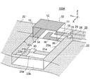
- FIG. 5 is a schematic perspective view showing the configuration of the antenna device according to the second embodiment of the present invention.
- the frequency adjusting element 30 is located at the center in the width direction (Y direction) in the ground clearance region 23a and the length of one wiring pattern 31a. Is characterized by a long period. There is no change in the position of the frequency adjusting element 30 in the X direction, and the position in the Y direction is simply shifted. In this configuration, the sensitivity of the resonance frequency is slightly higher than that of the antenna device 100, but the resonance frequency can be finely adjusted even when a commercially available chip capacitor is used.
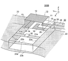
- FIG. 6 is a schematic perspective view showing the configuration of the antenna device according to the third embodiment of the present invention.
- the antenna device 200 ⁇ / b> A according to the third embodiment has a symmetrical arrangement of the frequency adjustment elements 30 compared to the antenna device 100 according to the first embodiment, and one end of the frequency adjustment element 30 is It is connected to the edge line 22c of the ground pattern.
- the frequency adjusting element 30 in the first embodiment, is biased toward the edge line 22a, whereas in the third embodiment, the frequency adjusting element 30 is biased toward the edge line 22c. It is characterized by being. In this configuration, the same characteristics as those of the antenna device 100 can be obtained, and fine adjustment of the resonance frequency using a commercially available chip capacitor is easy.
- FIG. 7 is a schematic perspective view showing the configuration of the antenna device according to the fourth embodiment of the present invention.
- the frequency adjustment element 30 is provided in the ground clearance region 23b on the back surface side of the printed circuit board 20 as compared with the antenna device 200A according to the third embodiment. It is characterized by being. One end of the frequency adjusting element 30 is connected to the edge line 22c of the ground pattern, and the other end is connected to the edge line 22b. That is, it has a shape that overlaps with the frequency adjustment element 30 in the antenna device 200A in plan view. Even with such a configuration, the same characteristics as those of the antenna devices 100A and 200A can be obtained, and the resonance frequency can be finely adjusted using a commercially available chip capacitor.
- FIG. 8 is a schematic perspective view showing the configuration of the antenna device according to the fifth embodiment of the present invention.
- one end of the wiring pattern 31b is connected to the edge line 22c instead of the edge line 22b of the ground pattern. It is characterized by forming a linear pattern as a whole. Even with such a configuration, characteristics similar to those of the antenna device 100A can be obtained, and the resonance frequency can be finely adjusted using a commercially available chip capacitor.
- the current propagation path from the feeding portion of the antenna element 10 to the frequency adjustment element 30 is slightly shorter, so the rate of change of the resonance frequency fc is slightly higher.
- the current contributing to the radiation of the antenna device is strongly distributed not only in the antenna element 10 but also around the boundary between the ground clearance region 23a of the printed circuit board 20 and the ground pattern 22. Therefore, if the current propagation path from the feeding portion of the antenna element 10 to the frequency adjustment element 30 can be lengthened, it can be estimated that the rate of change of the resonance frequency fc can be reduced.
- FIG. 9 is a schematic perspective view showing the configuration of the antenna device according to the sixth embodiment of the present invention.
- the position of the frequency adjusting element 30 in the X direction is slightly closer to the antenna element 10 side than the antenna device 300A according to the fifth embodiment. It is characterized by this. Therefore, in this configuration, the sensitivity of the resonance frequency is slightly higher than that of the antenna device 300A, but the resonance frequency can be finely adjusted using a commercially available chip capacitor.
- FIG. 10 is a schematic perspective view showing the configuration of the antenna device according to the seventh embodiment of the present invention.
- the frequency adjusting element 30 is provided near the edge line 22a of the ground pattern, and both ends of the frequency adjusting element 30 are connected to the wiring patterns 31a and 31b. It is characterized by being connected to the edge line 22a. Even with such a configuration, fine adjustment of the resonance frequency using a commercially available chip capacitor is possible.
- FIG. 11 is a schematic perspective view showing the configuration of the antenna device according to the seventh embodiment of the present invention.
- the antenna device 400B according to the seventh embodiment has a bilaterally symmetric relationship with the antenna device 400A, and the frequency adjustment element 30 is provided near the edge line 22c of the ground pattern. Both ends are connected to the edge line 22c through wiring patterns 31a and 31b. Even with such a configuration, fine adjustment of the resonance frequency using a commercially available chip capacitor is possible.
- FIG. 12 is a schematic perspective view showing the configuration of the antenna device according to the eighth embodiment of the present invention.
- the antenna device 500A according to the eighth embodiment is characterized in that the frequency adjustment element 30 is arranged closer to the antenna element 10 than the antenna device 300A according to the fifth embodiment. It is said. Both ends of the frequency adjusting element 30 are connected to the edge line 22b of the ground pattern via the wiring patterns 31a and 31b.
- the frequency adjusting element 30 according to the present embodiment does not satisfy La ⁇ Lb, and is resonant.
- the sensitivity of the frequency is relatively high, fine adjustment of the resonance frequency using a commercially available chip capacitor is possible even with such a configuration.
- FIG. 13 is a schematic perspective view showing the configuration of the antenna device according to the ninth embodiment of the present invention.
- both ends of the frequency adjusting element 30 are both connected to the lands in the antenna mounting area 23a as compared with the antenna device 500A according to the eighth embodiment. It is characterized by being. Specifically, one end of the frequency adjusting element 30 is connected to the ground pattern 22 via the wiring pattern 31 a and the third land 26, and the other end is grounded via the wiring pattern 31 b and the first land 24. Connected to the pattern 22. As described above, in the antenna device 500B according to the present embodiment, each terminal of the frequency adjusting element 30 is not directly connected to the ground pattern. Even in such a configuration, a commercially available chip capacitor is used as in the antenna device 500A. It is possible to finely adjust the resonance frequency using.
- FIG. 14 is a schematic perspective view showing the configuration of the antenna device according to the tenth embodiment of the present invention.
- the frequency adjustment element 30 is connected to the land in the antenna mounting area 23a, compared to the antenna device 500B according to the ninth embodiment. It is characterized by being. Specifically, one end of the frequency adjusting element 30 is connected to the edge line 22a of the ground pattern 22 via the wiring pattern 31a, and the other end is connected to the ground pattern 22 via the wiring pattern 31b and the first land 24. It is connected. Even with such a configuration, the resonance frequency can be finely adjusted using a commercially available chip capacitor in the same manner as the antenna devices 500A and 500B.
- FIG. 15 is a schematic perspective view showing the configuration of the antenna device according to the eleventh embodiment of the present invention.
- the antenna device 500D according to the eleventh embodiment has a bilaterally symmetric relationship with the antenna device 500C, and only one end of the frequency adjustment element 30 is compared with the antenna device 500B according to the ninth embodiment. Is connected to a land in the antenna mounting area 23a. Specifically, one end of the frequency adjusting element 30 is connected to the edge line 22c of the ground pattern 22 via the wiring pattern 31b, and the other end is connected to the ground pattern 22 via the wiring pattern 31a and the third land 26. It is connected. Even with such a configuration, the resonance frequency can be finely adjusted using a commercially available chip capacitor as in the antenna devices 500A to 500C. Since antenna device 500A has the longest current propagation path among antenna devices 500A to 500D, the rate of change in resonance frequency fc of antenna device 500A is the smallest (dull).
- FIG. 16 is a schematic perspective view showing the configuration of the antenna device according to the twelfth embodiment of the present invention.
- the antenna device 600 according to the thirteenth embodiment includes a plurality of frequency adjustment elements, and the frequency adjustment element 30 of the antenna device 100 according to the first embodiment and the fourth embodiment. Is combined with the frequency adjusting element 30 of the antenna device 300B. According to this configuration, it is possible to arbitrarily select the change rate of the resonance frequency. In addition, various variations can be taken as a combination of two or more frequency adjusting elements.
- the antenna devices according to the first to twelfth embodiments have slightly different sensitivities to the resonance frequency fc depending on the layout of the frequency adjustment element 30, but the resonance frequency fc is changed by changing the element value of the frequency adjustment element.
- the resonance frequency can be easily fine-tuned using a commercially available chip component.
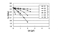
- FIG. 17 is a graph showing the simulation results of the frequency characteristics of each antenna device, in which the horizontal axis indicates the value of the capacitance C4 by the frequency adjustment element, and the vertical axis indicates the resonance frequency fc.
- Graphs G1 to G6 in FIG. 17 show the characteristics of the antenna devices 100, 100A, 300A, 300B, 500A, and 500B, respectively.
- the resonance frequency fc of each antenna device decreases as the capacitance C4 by the frequency adjustment element 30 increases.
- the rate of change of the resonance frequency fc increases as the frequency adjustment element 30 is closer to the antenna element 10.
- the resonance frequency fc remains so much even when the capacitance C ⁇ b> 4 is changed.
- the antenna device 500B as shown in the graph G6, the resonance frequency changes greatly only by changing the capacitance C4 slightly.
- the rate of change of the resonance frequency fc relative to the frequency adjustment element 30 varies depending on the position of the frequency adjustment element 30 and its pattern shape, and the sensitivity of the resonance frequency fc becomes less sensitive as the distance from the antenna element 10 increases.
- the current contributing to the radiation of the antenna device is strongly distributed not only in the antenna element 10 but also around the boundary between the ground clearance region 23a of the printed circuit board 20 and the ground pattern 22. Therefore, if the current propagation path from the feeding portion of the antenna element 10 to the frequency adjustment element 30 can be lengthened, it can be estimated that the rate of change of the resonance frequency fc can be reduced.
- FIG. 18 is a graph showing the simulation results of the frequency characteristics of each antenna device, and graphs G1, G7, and G8 show the characteristics of the antenna devices 100, 200A, and 200B, respectively.
- the rate of change of the resonance frequency fc with respect to the capacitance C4 is substantially the same for the antenna devices 100, 200A, and 200B.
- the resonance frequency characteristics hardly change even if the position of the frequency adjusting element 30 in the Y direction is reversed left and right or the positions of the front and back surfaces are reversed. I understand that.
- FIG. 19 is a schematic perspective view showing the configuration of the antenna device according to the thirteenth embodiment of the present invention.
- FIG. 20 is a development view of the antenna element.
- the terminal electrode 16 of the antenna element 10 is not L-shaped but rectangular, and has the same shape as the terminal electrode 15. Therefore, the conductor pattern formed on each surface of the base 11 of the antenna element 10 has a symmetrical shape with respect to the center line extending in the longitudinal direction of the base 11. Further, although not particularly limited, the positions of the terminal electrodes 15 and 16 according to the present embodiment are slightly closer to the center and do not contact the long side of the bottom surface 11b. Since other configurations are the same as those of the antenna device 100 according to the first embodiment, the same components are denoted by the same reference numerals, and detailed description thereof is omitted.
- the conductor patterns formed on each surface of the base body 11 are bilaterally symmetric. Therefore, the antenna device 700 is based on an axis (Z axis) perpendicular to the upper and lower surfaces of the base body 11. Even if the orientation of the element 10 is rotated by 180 degrees, the conductor pattern shape of the antenna element 10 viewed from the edge side of the printed circuit board 20 is substantially the same. Therefore, the antenna characteristics do not change greatly depending on the orientation of the antenna element 10, and the antenna design can be facilitated.
- FIG. 21 is a schematic perspective view showing the configuration of the antenna device according to the fourteenth embodiment of the present invention.
- FIG. 22 is a development view of the antenna element.
- the terminal electrode 16 of the antenna element 10 is omitted, and instead, the terminal electrode 15 has the same shape as the terminal electrode 14. That is, the second terminal electrode 15 is formed over the entire width direction of the bottom surface 11 b, similarly to the first terminal electrode 14. Also in this case, the conductor pattern of the antenna element 10 has a symmetrical shape. Since the terminal electrode 16 is omitted, there is no capacitance C2 formed by the gap between the upper conductor pattern 12 and the terminal electrode 16. Since other configurations are the same as those of the antenna device 100 according to the first embodiment, the same components are denoted by the same reference numerals, and detailed description thereof is omitted.
- the conductor patterns formed on the respective surfaces of the base body 11 of the antenna device 800 according to the present embodiment are symmetrical with respect to the center line extending in the longitudinal direction of the base body 11. Even if the orientation of the antenna element 10 is rotated 180 degrees with respect to the axis perpendicular to the Z axis (Z axis), the conductor pattern shape of the antenna element 10 viewed from the edge side of the printed circuit board 20 is substantially the same. Therefore, the antenna characteristics do not change greatly depending on the orientation of the antenna element 10, and the antenna design can be facilitated.
- FIG. 23 is an antenna device according to the fifteenth embodiment of the present invention, and is a schematic plan view showing a modification of the land pattern.
- the antenna device is characterized in that the land 26 in the antenna mounting area 27 is not rectangular but L-shaped.
- the terminal electrode 16 on the antenna element 10 side may be L-shaped as shown in FIG. 2 or may be rectangular as shown in FIG.
- the pattern formed between the antenna element 10 and the printed circuit board 20 is L-shaped, so that electromagnetic coupling with the ground pattern can be weakened, and radiation Efficiency can be improved.
- an electrode pattern is formed between the substrate 11 and the printed board 20 with terminal electrodes or lands, the effect is the same. Note that it is preferable to form the terminal electrode on the bottom surface of the substrate 11 because variation in characteristics due to positional deviation of the substrate 11 when the substrate 11 is placed on the printed circuit board 20 can be reduced.
- a chip capacitor is used as the frequency adjusting element, but a chip inductor may be used instead of the chip capacitor.
- the resonance frequency fc can be adjusted to the high frequency side. Further, the resonance frequency fc increases as the inductance value decreases.
- the fc adjustment method toward the high frequency side can be adjusted by using a capacitance to resonate in a higher order mode (harmonic), and by using both methods, fc adjustment can be performed continuously over a wide band. .
- FIG. 24 is an equivalent circuit diagram of the antenna device according to the sixteenth embodiment of the present invention.
- the antenna device 900 uses a chip inductor as the frequency adjusting element 30.
- a chip inductor As shown in FIG. 24, the antenna device 900 according to the present embodiment uses a chip inductor as the frequency adjusting element 30.
- this equivalent circuit is obtained.
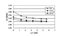
- FIG. 25 is a graph showing the frequency characteristics of the antenna device.
- Graphs G9 to G11 show the frequencies of the antenna device 100 shown in FIG. 1, the antenna device 100A shown in FIG. 5, and the antenna device 300A shown in FIG.
- the change rate of the resonance frequency fc when the capacitance C4 as the adjustment element 30 is replaced with the inductance L1 is shown.
- the resonance frequency decreases as the inductance L1 increases.
- the rate of change of the resonance frequency fc increases as the frequency adjustment element 30 approaches the antenna element 10.
- the resonance frequency fc does not change so much even if the inductance L1 is changed.
- the resonance frequency fc changes greatly only by slightly increasing the inductance L1.
- the rate of change of the resonance frequency fc varies greatly depending on the inductance of the frequency adjustment element 30.
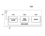
- FIG. 26 is a block diagram showing an example of the configuration of a wireless communication device using the antenna device according to the present invention.
- the wireless communication device 1000 includes an antenna element 10, a matching circuit 1001 that adjusts the input impedance of the antenna element 10, a wireless circuit unit 1002 that outputs a radio frequency signal, a matching circuit unit 1001, and a wireless circuit. And a control unit 1003 for controlling the circuit unit 1002.
- the matching circuit 1001, the radio circuit unit 1002, and the control unit 1003 constitute one communication circuit unit, and are mounted on the printed circuit board 20 together with the antenna element 10.
- the base 11 of the antenna element 10 is a rectangular parallelepiped, but it is not necessary to be a strict rectangular parallelepiped, and may be roughly a rectangular parallelepiped. Therefore, it may have a partial notch, a penetrating or non-penetrating hole, and the like.
- the ground clearance region 23a is rectangular has been described as an example.
- the ground clearance region 23a is not necessarily a strict rectangle, and may be roughly a rectangle. Since the ground pattern around the ground clearance area 23a actually has a complicated shape depending on the layout of various components mounted on the printed circuit board 20, each side of the ground clearance area 23a needs to be a complete straight line. There may be some uneven portions.
- the ground clearance region 23a is formed as a flat insulating region. However, it is also effective to lower the dielectric constant by providing a recess or a through hole in the ground clearance region 23a. It can be used in combination with each embodiment.
- the terminal electrodes 14 to 16 are provided on the bottom surface 11b of the base 11 of the antenna element 10, and the antenna element 10 is solder-mounted on the lands 24 to 26 on the printed circuit board 20.
- the invention is not limited to such a configuration, and the terminal electrodes 14 to 16 on the bottom surface 11b of the substrate 11 may be omitted.
- the electrode pattern sandwiched between the bottom surface of the base 11 of the antenna element 10 and the printed board consists of only the land patterns 14 to 16, but can function as an antenna device according to the present invention.
- the antenna element 10 can be fixed with an adhesive, for example.
Landscapes
- Engineering & Computer Science (AREA)
- Microelectronics & Electronic Packaging (AREA)
- Details Of Aerials (AREA)
- Support Of Aerials (AREA)
- Waveguide Aerials (AREA)
Abstract
Description
11 基体
11a 基体の上面
11b 基体の底面
11c,11d,11e,11f 基体の側面
12 上面導体パターン
13 側面導体パターン
14,15,16 端子電極
20 プリント基板
20a プリント基板の表面
20b プリント基板の裏面
20e プリント基板のエッジ
21 絶縁基板
22 グランドパターン
22a,22b,22c グランドパターンのエッジライン
23a,23b グランドクリアランス領域
24,25,26 ランド
27 アンテナ実装領域
28 給電ライン
29 インピーダンス調整素子
30 周波数調整素子
31a 配線パターン
31b 配線パターン
100,100A アンテナ装置
200,200A,200B アンテナ装置
300A,300B アンテナ装置
400A,400B アンテナ装置
500A,500B,500C,500D アンテナ装置
600 アンテナ装置
700 アンテナ装置
800 アンテナ装置
900 アンテナ装置
1000 無線通信機
1001 マッチング回路
1002 無線回路部
1003 制御部
C1~C4 キャパシタンス
L1 インダクタンス
Claims (12)
- アンテナ素子と、前記アンテナ素子が実装されたプリント基板とを備え、
前記アンテナ素子は、
誘電体からなる基体と、
前記基体の少なくとも一つの面に形成された放射導体とを備え、
前記プリント基板は、
一辺が当該プリント基板のエッジに接し、他の三辺がグランドパターンのエッジラインに囲まれた略矩形状のグランドクリアランス領域と、
前記グランドクリアランス領域内に設けられたアンテナ実装領域と、
前記グランドクリアランス領域内に設けられた少なくとも一つの周波数調整素子とを備え、
前記周波数調整素子は、前記プリント基板のエッジから見て前記アンテナ実装領域よりも遠くに設けられたキャパシタ又はインダクタのチップ部品を含むことを特徴とするアンテナ装置。 - 前記グランドパターンのエッジラインは、
前記プリント基板のエッジと直交する第1のエッジラインと、
前記プリント基板のエッジと対向する第2のエッジラインと、
前記第1のエッジラインと対向する第3のエッジラインを有し、
前記周波数調整素子から前記第2のエッジラインまでの距離は、前記前記周波数調整素子から前記アンテナ実装領域までの距離よりも短いことを特徴とする請求項1に記載のアンテナ装置。 - 前記グランドクリアランス領域内における前記周波数調整素子の位置は、前記第1のエッジライン側又は前記第3のエッジライン側に偏っていることを特徴とする請求項2に記載のアンテナ装置。
- 前記周波数調整素子の一端及び他端は、それぞれ前記第1乃至第3のエッジラインのいずれかに接続されていることを特徴とする請求項2に記載のアンテナ装置。
- 前記周波数調整素子の一端は、第1の配線パターンを介して前記第1のエッジラインに接続されており、
前記周波数調整素子の他端は、第2の配線パターンを介して前記第2のエッジラインに接続されていることを特徴とする請求項4に記載のアンテナ装置。 - 前記基体の底面と前記プリント基板に挟まれた第1及び第2の電極パターンをさらに備え、
前記第1の電極パターンは前記グランドパターンに接続されており、
前記第2の電極パターンは給電ラインに接続されていることを特徴とする請求項1に記載のアンテナ装置。 - 前記第1及び第2の電極パターンは、前記アンテナ素子の前記基体の底面に形成された第1及び第2の端子電極であることを特徴とする請求項6に記載のアンテナ装置。
- 前記プリント基板は、前記第1及び第2の端子電極に対応して前記アンテナ実装領域内に設けられた第1及び第2のランドをさらに備え、
前記第1の端子電極は前記第1のランドを介して前記グランドパターンに接続されており、
前記第2の端子電極は前記第2のランドを介して給電ラインに接続されていることを特徴とする請求項7に記載のアンテナ装置。 - 前記アンテナ素子は、前記基体の底面に形成された第3の端子電極をさらに備え、
前記プリント基板は、前記第3の端子電極に対応して前記アンテナ実装領域内に設けられた第3のランドをさらに備え、
前記第3の端子電極は前記第3のランドを介して前記グランドパターンに接続されていることを特徴とする請求項8に記載のアンテナ装置。 - 前記第3の端子電極及び前記第3のランドの少なくとも一方はL字形であり、開放端が前記プリント基板の前記エッジ側を向いていることを特徴とする請求項9に記載のアンテナ装置。
- 前記アンテナ素子の前記基体の表面に形成された導体パターンは、前記基体の長手方向に延びる中心線を基準として左右対称であることを特徴とする請求項9に記載のアンテナ装置。
- 通信回路部と、
前記通信回路部に接続されたアンテナ素子と、
前記通信回路部及び前記アンテナ素子が実装されたプリント基板とを備え、
前記アンテナ素子は、
誘電体からなる基体と、
前記基体の少なくとも一つの面に形成された放射導体とを備え、
前記プリント基板は、
一辺が当該プリント基板のエッジに接し、他の三辺がグランドパターンのエッジラインに囲まれた略矩形状のグランドクリアランス領域と、
前記グランドクリアランス領域内に設けられたアンテナ実装領域と、
前記グランドクリアランス領域内に設けられた少なくとも一つの周波数調整素子とを備え、
前記周波数調整素子は、前記プリント基板のエッジから見て前記アンテナ実装領域よりも遠くに設けられたキャパシタ又はインダクタのチップ部品を含むことを特徴とする無線通信機。
Priority Applications (2)
| Application Number | Priority Date | Filing Date | Title |
|---|---|---|---|
| US13/637,836 US9225057B2 (en) | 2010-04-01 | 2011-03-30 | Antenna apparatus and wireless communication device using same |
| CN201180017958.6A CN102834967B (zh) | 2010-04-01 | 2011-03-30 | 天线装置以及使用其的无线通信机 |
Applications Claiming Priority (2)
| Application Number | Priority Date | Filing Date | Title |
|---|---|---|---|
| JP2010-085543 | 2010-04-01 | ||
| JP2010085543A JP5375719B2 (ja) | 2010-04-01 | 2010-04-01 | アンテナ装置及びこれを用いた無線通信機 |
Publications (1)
| Publication Number | Publication Date |
|---|---|
| WO2011125707A1 true WO2011125707A1 (ja) | 2011-10-13 |
Family
ID=44762650
Family Applications (1)
| Application Number | Title | Priority Date | Filing Date |
|---|---|---|---|
| PCT/JP2011/057961 Ceased WO2011125707A1 (ja) | 2010-04-01 | 2011-03-30 | アンテナ装置及びこれを用いた無線通信機 |
Country Status (4)
| Country | Link |
|---|---|
| US (1) | US9225057B2 (ja) |
| JP (1) | JP5375719B2 (ja) |
| CN (1) | CN102834967B (ja) |
| WO (1) | WO2011125707A1 (ja) |
Families Citing this family (12)
| Publication number | Priority date | Publication date | Assignee | Title |
|---|---|---|---|---|
| JP5711318B2 (ja) * | 2013-08-05 | 2015-04-30 | Tdk株式会社 | アンテナ装置及びこれを用いた無線通信機器 |
| EP3499641B1 (en) | 2014-02-12 | 2022-01-26 | Huawei Device Co., Ltd. | Antenna and mobile terminal |
| JP6453453B2 (ja) * | 2014-10-03 | 2019-01-16 | テレフオンアクチーボラゲット エルエム エリクソン(パブル) | D2d動作のための送信機及び/又は受信機の決定 |
| WO2018101104A1 (ja) * | 2016-11-29 | 2018-06-07 | 株式会社村田製作所 | アンテナ装置 |
| US10516207B2 (en) * | 2017-05-17 | 2019-12-24 | Nxp B.V. | High frequency system, communication link |
| CN107706500B (zh) * | 2017-11-22 | 2020-04-10 | 深圳市盛路物联通讯技术有限公司 | 天线装置 |
| EP3624263A1 (en) * | 2018-09-12 | 2020-03-18 | u-blox AG | A multiband patch antenna |
| CN112582794B (zh) * | 2019-09-27 | 2024-07-02 | 昌泽科技有限公司 | 一种结构改良的芯片型天线 |
| TWI714300B (zh) | 2019-10-07 | 2020-12-21 | 美律實業股份有限公司 | 迴路天線 |
| CN115426764B (zh) * | 2022-06-24 | 2025-07-22 | 上海移为通信技术股份有限公司 | 一种电子设备 |
| JP2024080801A (ja) * | 2022-12-05 | 2024-06-17 | Tdk株式会社 | アンテナ装置 |
| US20260066544A1 (en) * | 2024-08-27 | 2026-03-05 | Silicon Laboratories Inc. | Dual Band Tapered Slot and Loop Ground Edge Radiating Antenna Structure |
Citations (7)
| Publication number | Priority date | Publication date | Assignee | Title |
|---|---|---|---|---|
| JP2004194211A (ja) * | 2002-12-13 | 2004-07-08 | Kyocera Corp | 表面実装型アンテナおよびアンテナ装置 |
| JP2004282109A (ja) * | 2003-01-23 | 2004-10-07 | Sony Chem Corp | 電子機器及びアンテナ実装プリント配線基板 |
| JP2004304783A (ja) * | 2003-03-20 | 2004-10-28 | Hitachi Metals Ltd | 表面実装型チップアンテナ及びアンテナ装置、並びにこれらを搭載した通信機器 |
| JP2005236534A (ja) * | 2004-02-18 | 2005-09-02 | Fdk Corp | アンテナ |
| WO2006120763A1 (ja) * | 2005-05-13 | 2006-11-16 | Murata Manufacturing Co., Ltd. | アンテナ構造およびそれを備えた無線通信機 |
| JP2008252158A (ja) * | 2007-03-29 | 2008-10-16 | Tdk Corp | アンテナブロック、アンテナ装置及び無線通信機器 |
| WO2009081803A1 (ja) * | 2007-12-21 | 2009-07-02 | Tdk Corporation | アンテナ装置及びこれを用いた無線通信機 |
Family Cites Families (8)
| Publication number | Priority date | Publication date | Assignee | Title |
|---|---|---|---|---|
| EP1460715A1 (en) | 2003-03-20 | 2004-09-22 | Hitachi Metals, Ltd. | Surface mount type chip antenna and communication equipment using the same |
| JP4941202B2 (ja) * | 2007-09-26 | 2012-05-30 | Tdk株式会社 | アンテナ装置及びその特性調整方法 |
| CN101836329B (zh) * | 2007-10-26 | 2012-12-19 | Tdk株式会社 | 天线装置及使用该天线装置的无线通信机 |
| JP4924399B2 (ja) * | 2007-12-13 | 2012-04-25 | Tdk株式会社 | アンテナ装置及びこれを用いた無線通信機 |
| JP4784636B2 (ja) * | 2008-10-28 | 2011-10-05 | Tdk株式会社 | 表面実装型アンテナ及びこれを用いるアンテナ装置並びに無線通信機 |
| JP4645729B2 (ja) * | 2008-11-26 | 2011-03-09 | Tdk株式会社 | アンテナ装置、無線通信機、表面実装型アンテナ、プリント基板、並びに表面実装型アンテナ及びプリント基板の製造方法 |
| JP4788791B2 (ja) * | 2009-02-27 | 2011-10-05 | Tdk株式会社 | アンテナ装置 |
| JP5251610B2 (ja) * | 2009-03-03 | 2013-07-31 | Tdk株式会社 | アンテナ装置及びこれに用いるアンテナ素子 |
-
2010
- 2010-04-01 JP JP2010085543A patent/JP5375719B2/ja not_active Expired - Fee Related
-
2011
- 2011-03-30 US US13/637,836 patent/US9225057B2/en not_active Expired - Fee Related
- 2011-03-30 WO PCT/JP2011/057961 patent/WO2011125707A1/ja not_active Ceased
- 2011-03-30 CN CN201180017958.6A patent/CN102834967B/zh not_active Expired - Fee Related
Patent Citations (7)
| Publication number | Priority date | Publication date | Assignee | Title |
|---|---|---|---|---|
| JP2004194211A (ja) * | 2002-12-13 | 2004-07-08 | Kyocera Corp | 表面実装型アンテナおよびアンテナ装置 |
| JP2004282109A (ja) * | 2003-01-23 | 2004-10-07 | Sony Chem Corp | 電子機器及びアンテナ実装プリント配線基板 |
| JP2004304783A (ja) * | 2003-03-20 | 2004-10-28 | Hitachi Metals Ltd | 表面実装型チップアンテナ及びアンテナ装置、並びにこれらを搭載した通信機器 |
| JP2005236534A (ja) * | 2004-02-18 | 2005-09-02 | Fdk Corp | アンテナ |
| WO2006120763A1 (ja) * | 2005-05-13 | 2006-11-16 | Murata Manufacturing Co., Ltd. | アンテナ構造およびそれを備えた無線通信機 |
| JP2008252158A (ja) * | 2007-03-29 | 2008-10-16 | Tdk Corp | アンテナブロック、アンテナ装置及び無線通信機器 |
| WO2009081803A1 (ja) * | 2007-12-21 | 2009-07-02 | Tdk Corporation | アンテナ装置及びこれを用いた無線通信機 |
Also Published As
| Publication number | Publication date |
|---|---|
| US9225057B2 (en) | 2015-12-29 |
| JP2011217288A (ja) | 2011-10-27 |
| US20130088398A1 (en) | 2013-04-11 |
| CN102834967A (zh) | 2012-12-19 |
| CN102834967B (zh) | 2016-04-13 |
| JP5375719B2 (ja) | 2013-12-25 |
Similar Documents
| Publication | Publication Date | Title |
|---|---|---|
| JP5375719B2 (ja) | アンテナ装置及びこれを用いた無線通信機 | |
| US8421679B2 (en) | Antenna device and antenna element used therefor | |
| JP5333235B2 (ja) | アンテナ装置及びこれを用いた無線通信機 | |
| JP4788791B2 (ja) | アンテナ装置 | |
| US9190721B2 (en) | Antenna device | |
| JP5711318B2 (ja) | アンテナ装置及びこれを用いた無線通信機器 | |
| JP5726983B2 (ja) | チップ状アンテナ装置及び送受信用通信回路基板 | |
| CN102714358A (zh) | 天线及无线通信装置 | |
| KR101003014B1 (ko) | 칩 안테나를 위한 pcb 레이아웃 구조 및 이를 이용한 칩 안테나 장치 | |
| JP5251965B2 (ja) | アンテナ装置及びその周波数調整方法 | |
| JP2011061638A (ja) | アンテナ装置 | |
| TWI524589B (zh) | 低阻抗槽饋入天線 | |
| JP4924399B2 (ja) | アンテナ装置及びこれを用いた無線通信機 | |
| JP4132063B2 (ja) | 表面実装型アンテナおよびアンテナ装置ならびに共振周波数の調整方法 | |
| JP4766137B2 (ja) | アンテナ装置 | |
| JP2008252155A (ja) | アンテナ装置及びこれを用いた無線通信機器 | |
| JP4656158B2 (ja) | アンテナ装置 | |
| JP2009065565A (ja) | アンテナ | |
| JP2005191882A (ja) | アンテナ装置 |
Legal Events
| Date | Code | Title | Description |
|---|---|---|---|
| WWE | Wipo information: entry into national phase |
Ref document number: 201180017958.6 Country of ref document: CN |
|
| 121 | Ep: the epo has been informed by wipo that ep was designated in this application |
Ref document number: 11765607 Country of ref document: EP Kind code of ref document: A1 |
|
| NENP | Non-entry into the national phase |
Ref country code: DE |
|
| WWE | Wipo information: entry into national phase |
Ref document number: 13637836 Country of ref document: US |
|
| 122 | Ep: pct application non-entry in european phase |
Ref document number: 11765607 Country of ref document: EP Kind code of ref document: A1 |