WO2011122060A1 - 照明装置および表示装置 - Google Patents
照明装置および表示装置 Download PDFInfo
- Publication number
- WO2011122060A1 WO2011122060A1 PCT/JP2011/050413 JP2011050413W WO2011122060A1 WO 2011122060 A1 WO2011122060 A1 WO 2011122060A1 JP 2011050413 W JP2011050413 W JP 2011050413W WO 2011122060 A1 WO2011122060 A1 WO 2011122060A1
- Authority
- WO
- WIPO (PCT)
- Prior art keywords
- light
- guide plate
- light guide
- cross
- engaging portion
- Prior art date
- Legal status (The legal status is an assumption and is not a legal conclusion. Google has not performed a legal analysis and makes no representation as to the accuracy of the status listed.)
- Ceased
Links
Images




Classifications
-
- G—PHYSICS
- G02—OPTICS
- G02B—OPTICAL ELEMENTS, SYSTEMS OR APPARATUS
- G02B6/00—Light guides; Structural details of arrangements comprising light guides and other optical elements, e.g. couplings
- G02B6/0001—Light guides; Structural details of arrangements comprising light guides and other optical elements, e.g. couplings specially adapted for lighting devices or systems
- G02B6/0011—Light guides; Structural details of arrangements comprising light guides and other optical elements, e.g. couplings specially adapted for lighting devices or systems the light guides being planar or of plate-like form
- G02B6/0081—Mechanical or electrical aspects of the light guide and light source in the lighting device peculiar to the adaptation to planar light guides, e.g. concerning packaging
- G02B6/0086—Positioning aspects
- G02B6/0091—Positioning aspects of the light source relative to the light guide
-
- G—PHYSICS
- G02—OPTICS
- G02B—OPTICAL ELEMENTS, SYSTEMS OR APPARATUS
- G02B6/00—Light guides; Structural details of arrangements comprising light guides and other optical elements, e.g. couplings
- G02B6/0001—Light guides; Structural details of arrangements comprising light guides and other optical elements, e.g. couplings specially adapted for lighting devices or systems
- G02B6/0011—Light guides; Structural details of arrangements comprising light guides and other optical elements, e.g. couplings specially adapted for lighting devices or systems the light guides being planar or of plate-like form
- G02B6/0081—Mechanical or electrical aspects of the light guide and light source in the lighting device peculiar to the adaptation to planar light guides, e.g. concerning packaging
- G02B6/0086—Positioning aspects
- G02B6/0088—Positioning aspects of the light guide or other optical sheets in the package
Definitions
- the present invention relates to an illumination device such as a backlight unit and a display device (liquid crystal display device or the like) on which the illumination device is mounted.
- an illumination device such as a backlight unit and a display device (liquid crystal display device or the like) on which the illumination device is mounted.
- a backlight unit for supplying light to the liquid crystal display panel.
- the backlight unit desirably generates planar light that spreads over the entire area of the planar liquid crystal display panel.
- the backlight unit may include a light guide plate for mixing light of a built-in light source (for example, a light emitting element such as an LED) to a high degree.
- the light emitting surface 132L of the LED 132 of the LED module mj faces the light receiving surface 111Sa of the light guide plate 111 and faces the light receiving surface 111Sa.
- the light guide plate 111 causes multiple reflections of light inside and emits planar light from the top surface 111U.
- the axis pl formed on the light receiving surface 111Sa of the light guide plate 111 fits into the opening 131H formed in the mounting substrate 131. Thereby, the LED module mj does not shift along the thickness direction of the light guide plate 111 and the longitudinal direction of the light receiving surface 111Sa.
- the axis pl of the light guide plate 111 is along the light emission direction of the LED 132. Therefore, the LED module mj may fluctuate along this axial direction and the emission direction of the LED 132. That is, the distance between the light emitting surface 132L of the LED 132 and the light receiving surface 111Sa of the light guide plate 111 may change.
- the light emitted from the light guide plate 111 is unlikely to be an appropriate planar light that is assumed in design. For example, it becomes planar light including unevenness in the amount of light.
- the present invention has been made in view of the above situation. And the objective of this invention is providing the illuminating device which does not raise
- the illuminating device has a light source, a mounting substrate on which the light source is mounted, a light receiving surface facing the light emitting direction of the light source, receiving light through the light receiving surface, and extending in a direction intersecting the light emitting direction.
- a stator that contacts the overlapping mounting substrate and the light guide plate and fixes the mounting substrate and the light guide plate is included.
- the stator crosses the light emission direction from the light source, the mounting substrate and the light guide plate fixed by the stator do not move along the emission direction. Then, the distance between the light emitting surface of the light source mounted on the mounting substrate and the light receiving surface of the light guide plate does not change. Therefore, the light emitted from the light guide plate is likely to be an appropriate surface light assumed in design.
- the stator is, for example, a shaft connected to the mounting substrate, and the light guide plate is formed with an engaging portion that engages with the shaft.
- the lighting device includes a housing that accommodates the light source, the mounting substrate, the light guide plate, and the stator
- the stator is an axis that is continuous with the housing, and the light guide plate and the mounting substrate have the axis on the axis. It is desirable that engaging portions are formed.
- the lighting device preferably satisfies the following expression. RL ⁇ GL / 4
- RL the shortest distance from the light receiving surface to the engaging portion GL: the total length of the light guide plate in the direction along the light emitting direction of the light source.
- the light guide plate is thermally expanded by receiving light (heat) from the light source.
- thermal expansion is likely to occur with reference to the engaging portion in the light guide plate.
- Formula (1) is satisfy
- the engaging portion is not particularly limited, but is preferably a depression, a notch, or an opening.
- the cross-sectional shape of the engaging portion in the cross-sectional direction in the same plane direction as the light output surface of the light guide plate has a short side along the light output direction of the light source, and has a length orthogonal to the light output direction of the light source.
- the cross-sectional shape of the shaft has a width that closely contacts the interval between the long inner walls of the engaging portion.
- the distance between the light receiving surface of the light guide plate and the light source is not easily changed, but there is a margin between the engaging portion and the shaft in the direction orthogonal to the light emitting direction of the light source. Therefore, it is easy to attach the stator to the light guide plate.
- the light source supplies light to two opposite side surfaces of the light guide plate, and when these two side surfaces are light receiving surfaces, in order to ensure the ease of attaching the stator to the light guide plate, the following It may be like this.
- the cross-sectional shape of the engaging portion close to one light receiving surface side has a short side along the light emitting direction of the light source and the light of the light source
- the cross-sectional shape of the shaft that has a length perpendicular to the emission direction and fits in the engaging portion close to one light receiving surface side has a width that closely contacts the interval between the long inner walls of the engaging portion.
- the cross-sectional shape of the engaging portion close to the other light receiving surface side has a long side along the light emitting direction of the light source and a short side perpendicular to the light emitting direction of the light source, and the other light receiving surface side It is desirable that the cross-sectional shape of the shaft that fits in the engaging portion close to is a width that closely contacts the interval between the long inner walls of the engaging portion.
- the cross-sectional shape of the engaging portion in the cross-sectional direction in the same plane direction as the light exit surface of the light guide plate is an elliptical shape having a short axis along the short side of the engaging portion, a long axis along the long side of the engaging portion, or
- the tongue shape including an ellipse is desirable, and the cross-sectional shape of the shaft is desirably a perfect circle that is in close contact with the interval between the long inner walls of the engaging portion.
- one cross-sectional shape of the engaging portion in the cross-sectional direction in the same plane direction as the light emitting surface of the light guide plate is the length along the light emitting direction of the light source, and the light source
- the cross-sectional shape of the shaft that fits in the engagement portion of the perfect circle is a perfect circle that is in close contact with the interval between the long inner walls of the engagement portion. Desirable.
- a display device including the above lighting device and a display panel that receives light from the light device can be said to be the present invention.
- the overlapping mounting substrate and light guide plate are stationary.
- the light guide plate does not vary with respect to the mounting board along the light emission direction of the light source mounted on the mounting board. For this reason, the distance between the light emitting surface of the light source mounted on the mounting substrate and the light receiving surface of the light guide plate does not change, and the light emitted from the light guide plate is likely to be the appropriate planar light assumed in design.
- FIG. 3 is an exploded perspective view of a liquid crystal display device.
- FIG. 2 is a two-view drawing in which a sectional view and a plan view of the backlight unit are shown.
- FIG. 3 is an exploded perspective view of a liquid crystal display device.
- FIG. 2 is a two-view drawing in which a sectional view and a plan view of the backlight unit are shown.
- These are top views of a light guide plate and an LED module.
- FIG. 6 is an exploded perspective view of a conventional backlight unit.
- FIG. 1 is an exploded perspective view of the liquid crystal display device 69 (for convenience, a reflection sheet 41 described later is omitted in FIG. 1 and is shown in a sectional view of FIG. 2 described later).
- the liquid crystal display device 69 includes a liquid crystal display panel 59 and a backlight unit 49 (note that the liquid crystal display panel 59 is protected by a frame-shaped bezel BZ).
- an active matrix substrate 51 including a switching element such as a TFT (Thin Film Transistor) and a counter substrate 52 facing the active matrix substrate 51 are bonded together with a sealant (not shown). Then, liquid crystal (not shown) is injected into the gap between the substrates 51 and 52.
- a switching element such as a TFT (Thin Film Transistor)
- a counter substrate 52 facing the active matrix substrate 51 are bonded together with a sealant (not shown). Then, liquid crystal (not shown) is injected into the gap between the substrates 51 and 52.
- a polarizing film 53 is attached to the light receiving surface side of the active matrix substrate 51 and the emission side of the counter substrate 52.
- the liquid crystal display panel 59 as described above displays an image using the change in transmittance caused by the inclination of the liquid crystal molecules.
- the backlight unit 49 includes an LED module [light source module] MJ, a light guide plate 11, a reflection sheet 41 (see FIG. 2), a backlight chassis 42, a diffusion plate 43, a prism sheet 44, and a lens sheet 45.
- the LED module MJ is a module that emits light, and includes a mounting board 31 and an LED (Light Emitting Diode) 32 mounted on the board surface of the mounting board 31.
- LED Light Emitting Diode
- the mounting substrate 31 is a plate-like and rectangular substrate, and a plurality of electrodes (not shown) are arranged on the mounting surface 31U. Then, the LED 32 is mounted on the electrodes arranged in a row.
- the backlight unit 49 is mounted with a single mounting substrate 31, and the extending direction of the mounting substrate 31 intersects the X direction (this is orthogonal to the X direction), and also in the emission direction of the LED 32.
- a direction that intersects (perpendicular to, etc.) a certain direction with the Y direction, the X direction, and the Y direction is defined as a Z direction.
- the LED 32 is mounted on an electrode (not shown) formed on the mounting surface of the mounting substrate 31 so as to receive light and emit light (the light emitting surface 32L of the LED 32 is in the direction of the substrate surface of the mounting substrate 31).
- the light emission direction of the LED 32 is along the substrate surface direction).
- a plurality of LEDs (light emitting elements, point light sources) 32 are mounted on the mounting substrate 31 in order to secure the light quantity.
- only a part of the LEDs 32 are shown for convenience.
- the light guide plate 11 is a plate-like member having a side surface 11S and a top surface 11U and a bottom surface 11B positioned so as to sandwich the side surface 11S. And one surface (light-receiving surface 11Sa) of the side surface 11S receives the light from the LED 32 by facing the light-emitting surface 32L of the LED 32. The received light is multiple-reflected inside the light guide plate 11 and is emitted outward from the top surface (exit surface) 11U as planar light.
- the reflection sheet 41 (see FIG. 2) is a sheet covered with the bottom surface 11B of the light guide plate 11, and the reflection surface of the sheet faces the bottom surface 11B of the light guide plate 11. Then, if there is leaked light from the bottom surface 11B of the light guide plate 11, the light is reflected back to the light guide plate 11 to prevent light loss.
- the backlight chassis (container) 42 is, for example, a box-shaped member that houses the reflection sheet 41, the light guide plate 11, and the LED module MJ, as well as the diffusion plate 43, the prism sheet 44, and the lens sheet. 45 is also accommodated.
- the diffusion plate 43 is an optical member that overlaps the top surface 11U of the light guide plate 11, and diffuses the light emitted from the light guide plate 11. That is, the diffusion plate 43 diffuses the planar light formed by the light guide plate 11 and spreads the light throughout the liquid crystal display panel 59.
- the prism sheet 44 is an optical member that overlaps the diffusion plate 43.
- the prism sheet 44 arranges, for example, triangular prisms extending in one direction (linear) in a direction intersecting with one direction in the sheet surface. Thereby, the prism sheet 44 deflects the radiation characteristic of the light from the diffusion plate 43.
- the lens sheet 45 is an optical member that overlaps the prism sheet 44.
- the lens sheet 45 disperses the fine particles that refract and scatter light inside. Thereby, the lens sheet 45 suppresses the light / dark difference (light quantity unevenness) without locally condensing the light from the prism sheet 44.
- the backlight unit 49 as described above converts the light from the plurality of LED modules MJ into planar light by the light guide plate 11 and passes the planar light through the plurality of optical members 43 to 45 to display the liquid crystal display. Supply to panel 59. Thereby, the non-light-emitting liquid crystal display panel 59 receives the light (backlight light) from the backlight unit 49 and improves the display function.
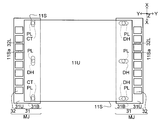
- FIG. 1 and FIG. 2 is a two-plane view showing a partial cross-sectional view and a plan view of the backlight unit 49 (the cross-sectional view is a cross-sectional view taken along the line AA ′ in FIG.
- the plan view mainly shows the light guide plate 11 and the LED module MJ for convenience).
- the light guide plate 11 is formed with a cutout CT and a recess DH. More specifically, the notch (engagement portion) CT is formed by the progress of the defect from the bottom surface 11B of the light guide plate 11 toward the top surface 11U, and the defect reaches the side surface 11S of the light guide plate 11. (However, the defect does not reach the top surface 11U).
- the depression (engagement portion) DH is formed by the progress of the defect from the bottom surface 11B of the light guide plate 11 toward the top surface 11U (however, the defect forming the depression DH is not the same as the notch CT. It does not reach the top surface 11U).
- the reflection sheet 41 is covered with the bottom surface of the light guide plate 11. Therefore, in the reflection sheet 41, a sheet opening 41H is formed at a location overlapping the notch CT and the depression DH in the light guide plate 11 (note that the size of the sheet opening 41H is the outer circumference and the depression of the notch CT. Larger than the outer circumference of DH). That is, the cutout CT and the recess DH in the light guide plate 11 are exposed without being blocked by the reflection sheet 41.
- a shaft (stator) PL protruding from the mounting surface 31U of the mounting substrate 31 is formed.
- the axis PL connected to the mounting substrate 31 corresponds to the notch CT and the recess DH in the light guide plate 11 (in essence, facing each other).
- the circumference (outer circumference) of the axis PL is smaller than the inner circumference of the notch CT and the inner circumference of the recess DH in the light guide plate 11. Therefore, when this axis PL fits into (is engaged with) the notch CT and the recess DH, the LED module MJ is immovable with respect to the light guide plate 11.
- the backlight chassis 42 includes a step 42P that can accommodate the mounting substrate 31 on the bottom surface 42B. More specifically, the backlight chassis 42 includes a step 42 ⁇ / b> P having a slightly larger area than the outer periphery of the mounting substrate 31. Then, when the mounting board 31 is fitted in the region of the step 42P that has dropped from the bottom surface 42B (the recessed step 42P), the mounting board 31 may move in the in-plane direction of the bottom surface 42B, and the side wall of the backlight chassis 42 42S and the wall 42Ps of the step 42P come into contact with each other and become immobile (the depth of the step 42P is slightly longer than the thickness of the mounting substrate 31).
- the backlight unit 49 includes the reflection sheet 41, the LED module MJ, and the backlight chassis 42, the backlight unit 49 is assembled as follows.
- the mounting substrate 31 in the LED module MJ is placed in the step 42P formed on the bottom surface 42B of the backlight chassis 42 with the non-mounting surface 31B (the back surface 31B of the mounting surface 31U) facing (the backlight chassis 42 and
- the mounting substrate 31 may be fixed with a double-sided tape or may be fixed with a screw. Then, the axis PL of the mounting substrate 31 rises with respect to the bottom surface 42B of the backlight chassis 42.
- the reflection sheet 41 covers the bottom surface 42B of the backlight chassis 42 so that the sheet opening 41H communicates with the shaft PL. Then, the axis PL is exposed through the sheet opening 41H of the reflection sheet 41.
- the light guide plate 11 is placed so that the notch CT and the recess DH fit into the axis PL.
- the light receiving surface 11Sa of the light guide plate 11 is designed to be at an appropriate distance without being in contact with the light emitting surface 32L of the LED 32 in a state where the axis PL is engaged with the notch CT and the recess DH. Yes.
- the axis PL is the light emitting direction from the LED 32.
- the mounting substrate 31 and the light guide plate 11 fixed by the axis PL do not move along the emission direction. Then, the distance between the light emitting surface 32L of the LED 32 mounted on the mounting substrate 31 and the light receiving surface 11Sa of the light guide plate 11 does not change. Therefore, the light emitted from the light guide plate 11 is likely to be an appropriate surface light assumed in design.
- the LED module MJ and the light guide plate 11 can be assembled while the positional relationship between the light receiving surface 11Sa and the light emitting surface 32L of the LED 32 is set to a predetermined position simply by fitting the light guide plate 11 to the axis PL.
- the light unit 49 can be easily assembled. In particular, when there are a plurality of shafts PL, the light guide plate 11 fitted to the shafts PL does not rotate.
- the widths of the cutout CT and the recess DH along the Y direction that is perpendicular to (intersects with) the light receiving surface 11Sa are the widths of the axis PL whose cross section (cross section perpendicular to the axial direction) is a perfect circle.
- the length is about the same as the diameter. Otherwise, even if the axis PL fits into the notch CT and the recess DH, the light guide plate 11 fluctuates with respect to the mounting substrate 31 in the Y direction, and the light receiving surface 11Sa and the light emitting surface 32L of the LED 32 This is because the distance changes.
- the width of the notch CT and the recess DH along the X direction which is the longitudinal direction of the light receiving surface 11Sa may be longer than the diameter of the axis PL. This is because, even if the axis PL fits into the notch CT and the recess DH, the light guide plate 11 varies with respect to the mounting substrate 31 in the Y direction, and the distance between the light receiving surface 11Sa and the light emitting surface 32L of the LED 32 does not change. It is. Moreover, it is also because the assembly of the LED module MJ and the light guide plate 11 becomes troublesome if there is no margin (space) between the axis PL and the cutout CT and the recess DH.
- the cross-sectional shapes of the cutout CT and the recess DH (specifically, the shape in the cross-sectional direction along the same plane direction as the top surface 11U of the light guide plate 11) have short sides along the light emitting direction of the LED 32, and the LED 32.
- a longitudinal axis perpendicular to the light emission direction of the light beam (for example, an elliptical shape having a short axis along the short side, an elliptical shape having a long axis extending along the longitudinal direction, or a tongue-shaped cross-sectional shape including the elliptical shape), and a transverse axis of the axis PL
- the surface shape may have a width (for example, a perfect circular cross-sectional shape) in close contact with the interval between the long inner walls of the notch CT and the recess DH.
- the width of the recess DH along the Y direction and the X direction may be equal to the diameter of the axis. This is because the light guide plate 11 does not fluctuate in the in-plane direction of the mounting substrate 31 (XY plane direction).
- the number of the axes PL may be one. This is because the movement of the light guide plate 11 in the XY plane direction relative to the mounting substrate 31 can be prevented even with one axis PL.
- the number of combinations of the engaging portion such as the notch CT or the recess DH and the shaft PL fitted thereto is not particularly limited.
- the position of the axis PL is not limited to the mounting surface 31U of the mounting substrate 31.
- the axis PL is not the mounting substrate 31 but the step 42P on the bottom surface 42B of the backlight chassis 42.
- the mounting substrate 31 must be provided with a substrate opening (engagement portion) 31H through the axis PL connected to the step 42P of the backlight chassis 42 ⁇ .
- the backlight chassis 42 not only accommodates the LED module MJ and the light guide plate 11, but also accommodates the shaft PL by connecting it to the step 42P of the bottom surface 42B.
- the shaft PL is engaged with the notch CT and the recess DH in the light guide plate 11 and the substrate opening 31H of the mounting substrate 31 to fix the overlapping mounting substrate 31 and light guide plate 11.
- the backlight unit 49 preferably satisfies the following expression (1).
- RL the shortest distance from the light receiving surface 11Sa of the light guide plate 11 to the cutout CT, or the shortest distance from the light receiving surface 11Sa of the light guide plate 11 to the recess DH GL: the light emitting direction of the LED 32 at the light guide plate 11
- the total length in the direction along (for example, the Y direction).
- the light guide plate 11 is made of resin, the light guide plate 11 is thermally expanded by receiving light (heat) from the LED 32.
- thermal expansion is likely to occur with reference to the notch CT and the recess DH in the light guide plate 11. Therefore, in order to ensure the quality of the planar light from the light guide plate 11, for example, it is desirable that thermal expansion does not occur in the vicinity of the center of the light guide plate 11 corresponding to the vicinity of the center of the planar light. Therefore, it is preferable that the above expression (1) is satisfied.
- the notch CT and the depression DH are formed near the end of the light guide plate 11 having little influence on the quality of the planar light, the surface is caused by the notch CT and the depression DH. The quality of the light is difficult to deteriorate.
- the cutout CT and the recess DH shown in FIGS. 1 and 2 may have a shape penetrating from the bottom surface 11B to the top surface 11U of the light guide plate 11 (for example, even if the recess DH is an opening). It doesn't matter) Further, out of the three openings 31H shown in FIGS. 3 and 4, the outer two openings 31H may be notches that are continuous with the short side of the mounting substrate 31.
- the mounting substrate 31 that is one member on the side close to the axis PL reaches the light guide plate 11 that is the other member. Therefore, it is sufficient that the hole 31H or the notch penetrates from the non-mounting surface 31B to the mounting surface 31U.
- the light guide plate 11 may be engaged with the approaching axis PL, it may be a notch CT, a recess DH, or an opening.
- the axis PL is not limited to a rod shape having a perfect circular or polygonal cross section, but is a cone shape (conical shape, pyramid shape, etc.), or a truncated cone shape (conical shape, truncated pyramid shape, etc.). It may be a protrusion.
- one indentation DH for example, an engaging portion at the center of three engaging portions arranged in parallel.
- Is a perfect circle in which the length along the light emission direction of the LED 32 and the length orthogonal to the light emission direction of the LED 32 are the same, and the cross-sectional shape of the axis PL that fits into the hollow DH of the perfect circle May be a perfect circle that is in close contact with the interval between the inner walls facing each other in the depression DH.
- the recess DH having a perfect circular cross section and the axis PL having a perfect circular cross section are in close contact with each other, so that the reference position is obtained.
- the remaining two cutouts CT are not in close contact with the axis PL in the X direction (in short, there is a margin between the cutout CT and the axis PL). Therefore, even if the recess DH serving as the reference position and the axis PL are fitted, the two cutouts CT and the axis PL are easily fitted. Therefore, the assembly of the LED module MJ and the light guide plate 11 does not become troublesome, and the light guide plate 11 does not vary in the in-plane direction (XY plane direction) of the mounting substrate 31.
- the LED module MJ is disposed on one side surface 11S of the light guide plate 11.
- the present invention is not limited to this.
- the LED module MJ may be disposed on two opposing side surfaces 11S. That is, the two side surfaces 11S facing each other at the light guide plate 11 may function as the light receiving surface 11Sa.
- the backlight unit 49 as shown in FIG. That is, of the two light receiving surfaces 11Sa, the cross-sectional shape of the engaging portion (the depression DH and the notch CT) close to the one light receiving surface 11Sa side has a short side along the light emitting direction of the LED 32, and the light of the LED 32 (For example, a short axis along the short side, an ellipse having a long axis along the long side, or a tongue-like cross-sectional shape including an ellipse), and a cross-sectional shape of the axis PL May have a width (for example, a perfect circular cross-sectional shape) that is in close contact with the interval between the longitudinal inner walls of the notch CT and the recess DH.
- a width for example, a perfect circular cross-sectional shape
- the shape of the engaging portion (dent DH) close to the other light receiving surface 11Sa side has a length along the light emitting direction of the LED 32 and is orthogonal to the light emitting direction of the LED 32.
- the cross-sectional shape of the axis PL is in close contact with the distance between the long inner walls in the recess DH. It is preferable to have a width (for example, a perfect circular cross-sectional shape).
- the light guide plate 11 is immovable with respect to the mounting substrate 31 in the Y direction by fitting the axis PL into the notch CT and the recess DH (that is, The distance between the light receiving surface 11Sa and the light emitting surface 32L of the LED 32 is constant).
- the extension is not excessively restricted (for example, due to the thermal expansion of the light guide plate 11).
- the axis PL does not break).
- the LED module MJ and the light guide plate 11 can be easily assembled because there is some margin between the axis PL and the recess DH.
- the number of LED modules MJ may be four as shown in FIG. That is, as shown in FIG. 7, the LED module MJ is arranged on the other two opposite side surfaces 11 ⁇ / b> S in addition to the two opposite side surfaces 11 ⁇ / b> S as shown in FIG. 6. May be. That is, all the side surfaces 11S in the light guide plate 11 may function as the light receiving surface 11Sa.
- the cross-sectional shape of the engaging portion (dent DH) close to one light receiving surface 11Sa side of the other two light receiving surfaces 11Sa is short along the light emitting direction of the LED 32. And has a length perpendicular to the light emission direction of the LED 32 (for example, an elliptical cross-sectional shape having a short axis along the short side and a long axis along the long side), and on one light receiving surface 11Sa side.
- the cross-sectional shape of the shaft PL that fits in the close engaging portion has a width that closely contacts the interval between the long inner walls of the recess DH (for example, a perfect circular cross-sectional shape).
- the cross-sectional shape of the engaging portion (indentation DH) close to the other light receiving surface 11Sa side has a length along the light emitting direction of the LED 32, and the light of the LED 32
- a shaft that has a short side perpendicular to the emission direction for example, an elliptical cross-sectional shape having a short axis along the short side and a long axis along the long side
- the cross-sectional shape of the PL has a width that closely adheres to the interval between the long inner walls in the recess DH (for example, a perfect circular cross-sectional shape).
Landscapes
- Physics & Mathematics (AREA)
- General Physics & Mathematics (AREA)
- Optics & Photonics (AREA)
- Planar Illumination Modules (AREA)
Abstract
導光板の受光面と光源との距離に変化を起こさせない照明装置、および、その照明装置を搭載する表示装置を提供する。光の出射方向に、受光面(11Sa)を向け、その受光面(11Sa)を介して光を受ける導光板(11)を搭載するバックライトユニット(49)では、軸(PL)は、LED(32)からの出射方向に対する交差方向に延びることで、重なり合う実装基板(31)および導光板(11)に対して接触し、その実装基板(31)と導光板(11)とを固定する。
Description
本発明は、例えば、バックライトユニットのような照明装置、および、その照明装置を搭載する表示装置(液晶表示装置等)に関する。
従来、非発光型の液晶表示パネル(表示パネル)を搭載する液晶表示装置では、その液晶表示パネルに対して光を供給するバックライトユニットも搭載される。バックライトユニットは、面状の液晶表示パネル全域に対して行き渡るような面状光を生成すると望ましい。そのために、バックライトユニットは、内蔵する光源(例えば、LEDのような発光素子)の光を高い度合いで混ぜ合わせるための導光板を含むことがある。
例えば、図8に示すように、特許文献1に開示されるバックライトユニット149では、LEDモジュールmjのLED132の発光面132Lは、導光板111の受光面111Saに向き、この受光面111Saに向けて光を供給する。そして、導光板111は、内部で光を多重反射させ、天面111Uから面状光を出射させる。
ところで、特許文献1でのバックライトユニット149では、導光板111の受光面111Saに形成された軸plが、実装基板131に形成された開孔131Hに嵌る。これにより、LEDモジュールmjは、導光板111の厚み方向および受光面111Saの長手方向に沿ってずれない。
しかしながら、導光板111の軸plは、LED132の光の出射方向に沿う。そのため、この軸方向およびLED132の出射方向に沿って、LEDモジュールmjは、変動するおそれがある。つまり、LED132の発光面132Lと導光板111の受光面111Saとの距離が変化するおそれがある。
そして、LED132の発光面132Lと導光板111の受光面111Saとの距離が所定の距離からずれてしまうと、導光板111から出射する光が、設計上、想定した適切な面状光になりにくく、例えば、光量ムラを含んだ面状光になってしまう。
本発明は、上記の状況を鑑みてなされたものである。そして、本発明の目的は、導光板の受光面と光源との距離に変化を起こさせない照明装置、および、その照明装置を搭載する表示装置を提供することにある。
照明装置は、光源、その光源を実装した実装基板、光源の光の出射方向に、受光面を向け、その受光面を介して光を受ける導光板、および、光の出射方向に対する交差方向に延びることで、重なり合う実装基板および導光板に対して接触し、実装基板と導光板とを固定する固定子、を含む。
このようになっていると、固定子が光源からの光の出射方向に交差していることから、その固定子によって固定される実装基板と導光板とは、出射方向に沿っては動かない。すると、実装基板に実装された光源の発光面と、導光板の受光面との距離は変化しない。したがって、導光板から出射する光が、設計上、想定した適切な面状光になりやすい。
なお、固定子は、例えば、実装基板に連なった軸であり、導光板には、その軸に係り合う係合部が形成される。
また、照明装置が、光源、実装基板、導光板、および固定子を収容する収容体を含む場合、固定子は、収容体に連なった軸であり、導光板および実装基板には、その軸に係り合う係合部が形成されると望ましい。
なお、照明装置は、以下の式を満たすと望ましい。
RL≦GL/4
ただし、
RL:受光面から係合部までの最短距離
GL:導光板にて、光源の光の出射方向に沿う方向での全長
である。
RL≦GL/4
ただし、
RL:受光面から係合部までの最短距離
GL:導光板にて、光源の光の出射方向に沿う方向での全長
である。
通常、導光板は、光源の光(熱)を受けることで熱膨張する。特に、導光板における係合部を基準にして、熱膨張が起きやすい。しかしながら、式(1)が満たされる場合、係合部は導光板の受光面近くに位置することになる。そのため、導光板が熱膨張して変形したとしても、面状光の中心付近に与える影響は少ない。したがって、照明装置は、高品質面状光を供給できる。
なお、係合部は、特に限定されるものではないが、窪み、切欠、または開孔であると望ましい。
また、導光板の光出射面と同面方向の断面方向における係合部の断面形状は、光源の光の出射方向に沿う短手を有するとともに、光源の光の出射方向に直交する長手を有し、軸の横断面形状は、係合部における長手の内壁同士の間隔に密着する幅を有すると望ましい。
このようになっていると、導光板の受光面と光源との距離は、変化しにくい一方で、光源の光の出射方向に対する直交方向では、係合部と軸との間に余裕ができる。そのため、導光板に対して固定子が取り付けやすい。
また、光源は、導光板における対向する2つの側面に光を供給することで、それら2つの側面が受光面となっている場合、導光板に対する固定子の取り付けやすさを確保すべく、以下のようになっていてもよい。
すなわち、導光板の光出射面と同面方向の断面方向において、一方の受光面側に近い係合部の断面形状は、光源の光の出射方向に沿う短手を有するとともに、光源の光の出射方向に直交する長手を有し、一方の受光面側に近い係合部に嵌る軸の横断面形状は、係合部における長手の内壁同士の間隔に密着する幅を有する。さらに、他方の受光面側に近い係合部の断面形状は、光源の光の出射方向に沿う長手を有するとともに、光源の光の出射方向に直交する短手を有し、他方の受光面側に近い係合部に嵌る軸の横断面形状は、係合部における長手の内壁同士の間隔に密着する幅を有する、と望ましい。
なお、導光板の光出射面と同面方向の断面方向における係合部の断面形状は、係合部の短手に沿う短軸、係合部の長手に沿う長軸を有する楕円形、または、楕円形を包含する舌形であると望ましく、さらには、軸の横断面形状は、係合部における長手の内壁同士の間隔に密着する真円であると望ましい。
また、複数の係合部が形成されている場合、導光板の光出射面と同面方向の断面方向における係合部の1つの断面形状は、光源の光の出射方向に沿う長さと、光源の光の出射方向に直交する長さとを同一にした真円であり、真円の係合部に嵌る軸の横断面形状は、係合部における長手の内壁同士の間隔に密着する真円であると望ましい。
このようになっていると、嵌り合う係合部と軸とが基準となるので、他の嵌り合う係合部と軸との間に余裕があってもよい。そのため、導光板に対して固定子が取り付けやすくなる。
また、以上の照明装置と、その明装置からの光を受光する表示パネルと、を含む表示装置も本発明といえる。
本発明によると、重なり合った実装基板と導光板とが不動になる。特に、実装基板に実装された光源の光の出射方向に沿って、導光板は実装基板に対して変動しない。そのため、実装基板に実装された光源の発光面と、導光板の受光面との距離は変化せず、導光板から出射する光が、設計上、想定した適切な面状光になりやすい。
[実施の形態1]
実施の一形態について、図面に基づいて説明すれば、以下の通りである。なお、便宜上、ハッチングや部材符号等を省略する場合もあるが、かかる場合、他の図面を参照するものとする。また、図面上での黒丸は紙面に対し垂直方向を意味する。
実施の一形態について、図面に基づいて説明すれば、以下の通りである。なお、便宜上、ハッチングや部材符号等を省略する場合もあるが、かかる場合、他の図面を参照するものとする。また、図面上での黒丸は紙面に対し垂直方向を意味する。
図1は液晶表示装置69の分解斜視図である(便宜上、後述する反射シート41は、図1で省略され、後述の図2の断面図に示される)。この図1に示すように、液晶表示装置69は、液晶表示パネル59とバックライトユニット49とを含む(なお、液晶表示パネル59は、枠状のベゼルBZによって保護される)。
液晶表示パネル59は、TFT(Thin Film Transistor)等のスイッチング素子を含むアクティブマトリックス基板51と、このアクティブマトリックス基板51に対向する対向基板52とをシール材(不図示)で貼り合わせる。そして、両基板51・52の隙間に液晶(不図示)が注入される。
なお、アクティブマトリックス基板51の受光面側、対向基板52の出射側には、偏光フィルム53が取り付けられる。そして、以上のような液晶表示パネル59は、液晶分子の傾きに起因する透過率の変化を利用して、画像を表示する。
次に、液晶表示パネル59の直下に位置するバックライトユニット49について説明する。バックライトユニット49は、LEDモジュール[光源モジュール]MJ、導光板11、反射シート41(図2参照)、バックライトシャーシ42、拡散板43、プリズムシート44、および、レンズシート45を含む。
LEDモジュールMJは光を発するモジュールであり、実装基板31と、この実装基板31の基板面上に実装されるLED(Light Emitting Diode)32と、を含む。
実装基板31は、板状かつ矩形状の基板であり、実装面31U上に、複数の電極(不図示)を並べる。そして、これらの列状に並ぶ電極上に、LED32が取り付けられる。なお、バックライトユニット49には、1本の実装基板31が搭載されており、その実装基板31の延び方向をX方向、このX方向に交差(直交等)し、かつ、LED32の出射方向でもある方向をY方向、X方向およびY方向に交差する(直交等)する方向をZ方向とする。
LED32は、実装基板31における実装面に形成された電極(不図示)に実装されることで電流の供給を受けて光を発する(なお、LED32の発光面32Lが、実装基板31の基板面方向に対して交差することで、LED32の光の出射方向は基板面方向に沿う)。また、光量確保のために、複数のLED(発光素子、点状光源)32が、実装基板31に実装されると望ましい。ただし、図面では便宜上、一部のLED32のみが示されているにすぎない。
導光板11は、側面11Sと、この側面11Sを挟持するように位置する天面11Uおよび底面11Bとを有する板状部材である。そして、側面11Sの一面(受光面11Sa)は、LED32の発光面32Lに面することで、LED32からの光を受光する。受光された光は、導光板11の内部で多重反射し、面状光として天面(出射面)11Uから外部に向けて出射する。
反射シート41(図2参照)は、導光板11における底面11Bにて覆われるシートで、シートにおける反射面は、導光板11の底面11Bに面する。そして、導光板11の底面11Bから、漏れだした光があれば、その光を導光板11に戻すように反射させ、光の損失を防ぐ。
バックライトシャーシ(収容体)42は、図1に示すように、例えば箱状の部材で、反射シート41、導光板11、LEDモジュールMJを収容するとともに、拡散板43、プリズムシート44、レンズシート45も収容する。
拡散板43は、導光板11の天面11Uに重なる光学部材であり、導光板11からの出射光を拡散させる。すなわち、拡散板43は、導光板11によって形成される面状光を拡散させて、液晶表示パネル59全域に光をいきわたらせる。
プリズムシート44は、拡散板43に重なる光学部材である。そして、このプリズムシート44は、一方向(線状)に延びる例えば三角プリズムを、シート面内にて、一方向に交差する方向に並べる。これにより、プリズムシート44は、拡散板43からの光の放射特性を偏向させる。
レンズシート45は、プリズムシート44に重なる光学部材である。そして、このレンズシート45は、光を屈折散乱させる微粒子を内部に分散させる。これにより、レンズシート45は、プリズムシート44からの光を、局所的に集光させることなく、明暗差(光量ムラ)を抑える。
そして、以上のようなバックライトユニット49は、複数のLEDモジュールMJの光を導光板11で面状光にし、その面状光を、複数枚の光学部材43~45に通過させて、液晶表示パネル59に供給する。これにより、非発光型の液晶表示パネル59は、バックライトユニット49からの光(バックライト光)を受光して表示機能を向上させる。
ここで、導光板11、反射シート41、LEDモジュールMJ、および、バックライトシャーシ42について、図1および図2を用いて詳説する。なお、図2は、バックライトユニット49の部分断面図と平面図とを示す2面図である(なお、断面図は、図1におけるA-A’先矢視断面方向の断面図であり、平面図は、便宜上、導光板11とLEDモジュールMJとを主として図示する)。
導光板11には、図1および図2に示すように、切欠CTおよび窪みDHが形成される。詳説すると、切欠(係合部)CTは、導光板11の底面11Bから天面11Uに向かって、欠損が進行するとともに、その欠損が導光板11の側面11Sにまで到達することで、形成される(ただし、欠損は天面11Uにまでは到達しない)。一方、窪み(係合部)DHは、導光板11の底面11Bから天面11Uに向かって、欠損が進行することで、形成される(ただし、切欠CT同様に、窪みDHを形成する欠損は天面11Uにまでは到達しない)。
反射シート41は、導光板11の底面に覆われる。そこで、この反射シート41には、導光板11における切欠CTと窪みDHとに重なる箇所に、シート開孔41Hが形成される(なお、シート開孔41Hの大きさは、切欠CTの外周および窪みDHの外周よりも大きい)。すなわち、導光板11における切欠CTおよび窪みDHは、反射シート41に遮られることなく、露出する。
LEDモジュールMJには、実装基板31の実装面31Uから突出する軸(固定子)PLが形成される。この実装基板31に連なった軸PLは、導光板11における切欠CTおよび窪みDHに対応する(要は、向かい合う)。さらに、この軸PLの軸周り(外周)は、導光板11における切欠CTの内周および窪みDHの内周よりも小さい。そのため、この軸PLが、切欠CTおよび窪みDHに嵌ると(係り合うと)、LEDモジュールMJは、導光板11に対して不動になる。
バックライトシャーシ42は、底面42Bに、実装基板31を収容可能な段差42Pを含む。詳説すると、実装基板31の外周よりも若干広い面積の段差42Pが、バックライトシャーシ42に含まれる。そして、底面42Bから落ち込んだこの段差42Pの領域(窪んだ段差42P)に、実装基板31が嵌ると、実装基板31は、底面42Bの面内方向に移動しようとしても、バックライトシャーシ42の側壁42Sおよび段差42Pの壁42Psに接触し、不動になる(なお、段差42Pの深さは、実装基板31の厚みよりも若干長い)。
これら反射シート41、LEDモジュールMJ、および、バックライトシャーシ42を含むバックライトユニット49であれば、そのバックライトユニット49は、以下のようにして、組み立てられる。
すなわち、バックライトシャーシ42の底面42Bに形成される段差42Pに、LEDモジュールMJにおける実装基板31が、非実装面31B(実装面31Uの裏面31B)を向けて収まる(なお、バックライトシャーシ42と実装基板31とは、例えば、両面テープで固定されてもよいし、ビス止めで固定されてもよい)。すると、バックライトシャーシ42の底面42Bに対して、実装基板31の軸PLが立ち上がる。
そして、この軸PLに、シート開孔41Hが通じるように、反射シート41が、バックライトシャーシ42の底面42Bを覆う。すると、軸PLが反射シート41のシート開孔41Hを通じて露出する。
さらに、この軸PLに、切欠CTおよび窪みDHが嵌るように、導光板11が置かれる。なお、このように、軸PLが切欠CTおよび窪みDHに係り合った状態で、導光板11の受光面11Saは、LED32の発光面32Lに接することなく、適切な距離になるように設計されている。
以上を踏まえると、LED32の光の出射方向に、受光面11Saを向け、その受光面11Saを介して光を受ける導光板11を搭載するバックライトユニット49では、軸PLは、LED32からの出射方向に対する交差方向に延びることで、重なり合う実装基板31および導光板11に対して接触し、その実装基板31と導光板11とを固定する。
このようになっていると、軸PLがLED32の出射方向に交差していることから、その軸PLによって固定される実装基板31と導光板11とは、出射方向に沿って動かない。すると、実装基板31に実装されたLED32の発光面32Lと、導光板11の受光面11Saとの距離は変化しない。したがって、導光板11から出射する光が、設計上、想定した適切な面状光になりやすい。
また、軸PLに対して、導光板11を嵌めるだけで、受光面11SaとLED32の発光面32Lとの位置関係を所定位置にしつつ、LEDモジュールMJと導光板11との組み立てができるので、バックライトユニット49の組み立てが容易である。特に、軸PLが複数有ると、それらの軸PLに嵌る導光板11は、回転することもない。
なお、受光面11Saに対して直交(交差)する方向であるY方向に沿う、切欠CTおよび窪みDHにおける幅は、横断面(軸方向に対して直交な断面)を真円とする軸PLの直径と同程度の長さである。このようになっていないと、軸PLが切欠CTおよび窪みDHに嵌ったとしても、Y方向にて、導光板11が実装基板31に対して変動し、受光面11SaとLED32の発光面32Lとの距離が変化してしまうためである。
ただし、受光面11Saの長手方向であるX方向に沿う、切欠CTおよび窪みDHにおける幅は、軸PLの直径よりも長くてかまわない。なぜなら、軸PLが切欠CTおよび窪みDHに嵌ったとしても、Y方向にて、導光板11が実装基板31に対して変動し、受光面11SaとLED32の発光面32Lとの距離が変化しないためである。また、軸PLと切欠CTおよび窪みDHとの間で、多少の余裕(空間)が無いと、LEDモジュールMJと導光板11との組み立てが煩わしくなってしまうためでもある。
すなわち、切欠CTおよび窪みDHの断面形状(詳説すると、導光板11における天面11Uと同面方向に沿う断面方向での形状)は、LED32の光の出射方向に沿う短手を有するとともに、LED32の光の出射方向に直交する長手を有し(例えば、短手に沿う短軸、長手に沿う長軸を有する楕円形、または、楕円形を包含する舌形の断面形状)、軸PLの横断面形状は、切欠CTおよび窪みDHにおける長手の内壁同士の間隔に密着する幅(例えば、真円の断面形状)を有するとよい。このようになっていれば、受光面11SaとLED32の発光面32Lとの距離が変化せずに、LEDモジュールMJと導光板11との組み立てが簡単になる。
しかし、全ての軸PLが真円の横断面を有する場合、Y方向およびX方向に沿う窪みDHの幅は、軸の直径と同程度であってもかまわない。このようになっていれば、導光板11が実装基板31の面内方向(XY面方向)において、変動しないためである。
なお、軸PLが真円の横断面ではなく多角形状の横断面を有し、その軸PLが窪みDHに隙間無く嵌る場合、軸PLの本数は1本であってもかまわない。1本の軸PLでも、実装基板31に対する導光板11のXY面方向の動きを防げるためである。要は、切欠CT、または窪みDHのような係合部と、それに嵌る軸PLとの組み合わせの数は、特に限定されない。
また、軸PLの位置は、実装基板31の実装面31Uに限定されるわけではない。例えば、図3分解斜視図および図4の2面図(図2と同様の図示の仕方)に示すように、軸PLが、実装基板31ではなく、バックライトシャーシ42の底面42Bにおける段差42Pに形成されてもよい{ただし、実装基板31には、バックライトシャーシ42の段差42Pに連なった軸PLを通じさせる基板開孔(係合部)31Hが形成されなくてはならない}。
すなわち、バックライトシャーシ42は、LEDモジュールMJおよび導光板11を収容するだけでなく、軸PLを底面42Bの段差42Pに連ねることで収容する。そして、この軸PLは、導光板11における切欠CTおよび窪みDH、並びに、実装基板31の基板開孔31Hに、係り合うことで、重なり合う実装基板31および導光板11を固定する。
また、図2および図4に示すように、バックライトユニット49では、以下の式(1)を満たすと望ましい。
RL≦GL/4 … 式(1)
ただし、
RL:導光板11の受光面11Saから切欠CTまでの最短距離、ま
たは、導光板11の受光面11Saから窪みDHまでの最短距
離
GL:導光板11にて、LED32の光の出射方向(例えば、Y方向
)に沿う方向での全長
である。
RL≦GL/4 … 式(1)
ただし、
RL:導光板11の受光面11Saから切欠CTまでの最短距離、ま
たは、導光板11の受光面11Saから窪みDHまでの最短距
離
GL:導光板11にて、LED32の光の出射方向(例えば、Y方向
)に沿う方向での全長
である。
通常、導光板11は樹脂製であるために、LED32の光(熱)を受けることで、熱膨張する。特に、導光板11における切欠CTおよび窪みDHを基準にして、熱膨張が起きやすい。そのため、導光板11からの面状光の品質を確保するためには、例えば、面状光の中心付近に相当する導光板11の中心付近で、熱膨張が起きないようにすると望ましい。そこで、上記の式(1)が満たされるとよい。このようになっていると、面状光の品質に対して影響の少ない導光板11の端付近に、切欠CTおよび窪みDHが形成されるので、それら切欠CTおよび窪みDHに起因して、面状光の品質が劣化しにくい。
[その他の実施の形態]
なお、本発明は上記の実施の形態に限定されず、本発明の趣旨を逸脱しない範囲で、種々の変更が可能である。
なお、本発明は上記の実施の形態に限定されず、本発明の趣旨を逸脱しない範囲で、種々の変更が可能である。
例えば、図1および図2に示される切欠CTおよび窪みDHは、導光板11における底面11Bから天面11Uまでを貫いた形状であってもかまわない(例えば、窪みDHが開孔であってもかまわない)。また、図3および図4に示される3つの開孔31Hのうち、外側の2つの開孔31Hは、実装基板31の短手に連なった切欠であってもかまわない。
要は、重なり合った実装基板31と導光板11とを不動にする場合、軸PLに近い側の一方の部材である実装基板31は、その軸PLを、他方の部材である導光板11に到達させるため、非実装面31Bから実装面31Uまでを貫いた開孔31Hまたは切欠であればよい。また、導光板11は、近づいてきた軸PLに係り合えばよいので、切欠CT、窪みDH、または開孔であればよい。
また、軸PLは、真円または多角形の横断面を有する棒状に限らず、錐体状(円錐状、角錐状等)、または、錐体台状(円錐台状、角錐台状等)の突起であってもかまわない。
また、複数の係合部(窪みDHおよび切欠CT)が形成されている場合、図5に示すように、1つの窪みDH(例えば、並列する3個の係合部の中心の係合部)の断面形状は、LED32の光の出射方向に沿う長さと、LED32の光の出射方向に直交する長さとを同一にした真円であり、その真円の窪みDHに嵌る軸PLの横断面形状は、窪みDHにて対向する内壁同士の間隔に密着する真円であってもよい。
このようになっていると、真円の断面を有する窪みDHと真円の断面を有する軸PLとが密着するので、基準位置になる。一方で、残り2つの切欠CTは、軸PLとX方向においては密着しない(要は、切欠CTと軸PLとの間に余裕がある)。そのため、基準位置となる窪みDHと軸PLとが嵌り合ったとしても、2つの切欠CTと軸PLとの嵌り合いが容易になされる。したがって、LEDモジュールMJと導光板11との組み立てが煩わしくならない上、導光板11が実装基板31の面内方向(XY面方向)において、変動しない。
また、以上では、導光板11における1つの側面11Sに対して、LEDモジュールMJが配置されていたが、これに限定されるものではない。例えば、図6に示すように、LEDモジュールMJが、対向する2つの側面11Sに配置されてもよい。すなわち、導光板11にて対向する2つの側面11Sが、受光面11Saとして機能してもよい。
そして、図6に示すようなバックライトユニット49では、以下のようになっていると望ましい。すなわち、2つの受光面11Saのうち、一方の受光面11Sa側に近い係合部(窪みDHおよび切欠CT)の断面形状は、LED32の光の出射方向に沿う短手を有するとともに、LED32の光の出射方向に直交する長手を有し(例えば、短手に沿う短軸、長手に沿う長軸を有する楕円形、または、楕円形を包含する舌形の断面形状)、軸PLの横断面形状は、切欠CTおよび窪みDHにおける長手の内壁同士の間隔に密着する幅(例えば、真円の断面形状)を有するとよい。
さらに、2つの受光面11Saのうち、他方の受光面11Sa側に近い係合部(窪みDH)の形状は、LED32の光の出射方向に沿う長手を有するとともに、LED32の光の出射方向に直交する短手を有し(例えば、短手に沿う短軸、長手に沿う長軸を有する楕円形の断面形状)、軸PLの横断面形状は、窪みDHにおける長手の内壁同士の間隔に密着する幅(例えば、真円の断面形状)を有するとよい。
このようになっていると、一方の受光面11Sa側では、軸PLが切欠CTおよび窪みDHに嵌ることで、Y方向にて、導光板11が実装基板31に対して不動になる(すなわち、受光面11SaとLED32の発光面32Lとの距離が一定になる)。一方、他方の受光面11Sa側では、導光板11がLED32の光で熱膨張し、X方向に延びたとしても、その延びを過度に規制しない(例えば、導光板11の熱膨張に起因して、軸PLが折れたりしない)。その上、軸PLと窪みDHとの間で、多少の余裕があるために、LEDモジュールMJと導光板11との組み立てが簡単でもある。
また、LEDモジュールMJの数は、図7に示すように4個であってもかまわない。すなわち、図7に示すように、LEDモジュールMJが、図6に示されるような対向する2つの側面11Sに対応して配置される他に、もう1つの対向する2つの側面11Sにも配置されてもよい。すなわち、導光板11における全ての側面11Sが、受光面11Saとして機能してもよい。
なお、図7に示すように、もう1つの2つの受光面11Saのうち、一方の受光面11Sa側に近い係合部(窪みDH)の断面形状は、LED32の光の出射方向に沿う短手を有するとともに、LED32の光の出射方向に直交する長手を有し(例えば、短手に沿う短軸、長手に沿う長軸を有する楕円形の断面形状)、かつ、一方の受光面11Sa側に近い係合部に嵌る軸PLの横断面形状は、窪みDHにおける長手の内壁同士の間隔に密着する幅を有する(例えば、真円の断面形状)。
さらに、もう1つの2つの受光面11Saのうち、他方の受光面11Sa側に近い係合部(窪みDH)の断面形状は、LED32の光の出射方向に沿う長手を有するとともに、LED32の光の出射方向に直交する短手を有し(例えば、短手に沿う短軸、長手に沿う長軸を有する楕円形の断面形状)、かつ、一方の受光面11Sa側に近い係合部に嵌る軸PLの横断面形状は、窪みDHにおける長手の内壁同士の間隔に密着する幅を有する(例えば、真円の断面形状)。
PL 軸(固定子)
CT 切欠(係合部)
DH 窪み(係合部)
HL 開孔(係合部)
11 導光板
11U 導光板の天面
11B 導光板の底面
11S 導光板の側面
11Sa 導光板の受光面
MJ LEDモジュール
31 実装基板
31U 実装面
31B 非実装面
31H 実装基板の開孔(係合部)
32 LED(光源)
32L LEDの発光面
41 反射シート
42 バックライトシャーシ(収容体)
42B バックライトシャーシの底面
42P バックライトシャーシの底面における段差
42Ps 段差の壁
42S バックライトシャーシの側壁
43 拡散板
44 プリズムシート
45 レンズシート
49 バックライトユニット(照明装置)
59 液晶表示パネル(表示パネル)
69 液晶表示装置(表示装置)
CT 切欠(係合部)
DH 窪み(係合部)
HL 開孔(係合部)
11 導光板
11U 導光板の天面
11B 導光板の底面
11S 導光板の側面
11Sa 導光板の受光面
MJ LEDモジュール
31 実装基板
31U 実装面
31B 非実装面
31H 実装基板の開孔(係合部)
32 LED(光源)
32L LEDの発光面
41 反射シート
42 バックライトシャーシ(収容体)
42B バックライトシャーシの底面
42P バックライトシャーシの底面における段差
42Ps 段差の壁
42S バックライトシャーシの側壁
43 拡散板
44 プリズムシート
45 レンズシート
49 バックライトユニット(照明装置)
59 液晶表示パネル(表示パネル)
69 液晶表示装置(表示装置)
Claims (10)
- 光源、
上記光源を実装した実装基板、
上記光源の光の出射方向に、受光面を向け、その受光面を介して光を受ける導光板、
および、
上記出射方向に対する交差方向に延びることで、重なり合う上記実装基板および上記導光板に対して接触し、上記実装基板と上記導光板とを固定する固定子、
を含む照明装置。 - 上記固定子は、上記実装基板に連なった軸であり、
上記導光板には、上記軸に係り合う係合部が形成される請求項1に記載の照明装置。 - 上記光源、上記実装基板、上記導光板、および上記固定子を収容する収容体が含まれており、
上記固定子は、上記収容体に連なった軸であり、
上記導光板および上記実装基板には、上記軸に係り合う係合部が形成される請求項1に記載の照明装置。 - 以下の式を満たす請求項2または3に記載の照明装置
RL≦GL/4
ただし、
RL:上記受光面から上記係合部までの最短距離
GL:上記導光板にて、上記光源の光の出射方向に沿う方向で
の全長
である。 - 上記係合部は、窪み、切欠、または開孔である請求項2~4のいずれか1項に記載の照明装置。
- 上記導光板の光出射面と同面方向の断面方向における上記係合部の断面形状は、上記光源の光の出射方向に沿う短手を有するとともに、上記光源の光の出射方向に直交する長手を有し、
上記軸の横断面形状は、上記係合部における上記長手の内壁同士の間隔に密着する幅を有する請求項5に記載の照明装置。 - 上記光源は、上記導光板における対向する2つの側面に光を供給することで、それら2つの側面が上記受光面となっており、
上記導光板の光出射面と同面方向の断面方向において、一方の受光面側に近い係合部の断面形状は、上記光源の光の出射方向に沿う短手を有するとともに、上記光源の光の出射方向に直交する長手を有し、一方の受光面側に近い係合部に嵌る上記軸の横断面形状は、上記係合部における上記長手の内壁同士の間隔に密着する幅を有し、
他方の受光面側に近い係合部の断面形状は、上記光源の光の出射方向に沿う長手を有するとともに、上記光源の光の出射方向に直交する短手を有し、他方の受光面側に近い係合部に嵌る上記軸の横断面形状は、上記係合部における上記長手の内壁同士の間隔に密着する幅を有する、請求項5に記載の照明装置。 - 上記導光板の光出射面と同面方向の断面方向における上記係合部の断面形状は、上記短手に沿う短軸、上記長手に沿う長軸を有する楕円形、または、楕円形を包含する舌形であり、
上記軸の横断面形状は、上記係合部における上記長手の内壁同士の間隔に密着する真円である請求項6または7に記載の照明装置。 - 複数の上記係合部が形成されている場合、上記導光板の光出射面と同面方向の断面方向における上記係合部の1つの断面形状は、上記光源の光の出射方向に沿う長さと、上記光源の光の出射方向に直交する長さとを同一にした真円であり、
上記真円の上記係合部に嵌る上記軸の横断面形状は、上記係合部における上記長手の内壁同士の間隔に密着する真円である請求項5に記載の照明装置。 - 請求項1~9のいずれか1項に記載の照明装置と、
上記照明装置からの光を受光する表示パネルと、
を含む表示装置。
Priority Applications (1)
| Application Number | Priority Date | Filing Date | Title |
|---|---|---|---|
| US13/580,007 US8911136B2 (en) | 2010-03-31 | 2011-01-13 | Illumination apparatus and display device |
Applications Claiming Priority (2)
| Application Number | Priority Date | Filing Date | Title |
|---|---|---|---|
| JP2010-080450 | 2010-03-31 | ||
| JP2010080450 | 2010-03-31 |
Publications (1)
| Publication Number | Publication Date |
|---|---|
| WO2011122060A1 true WO2011122060A1 (ja) | 2011-10-06 |
Family
ID=44711814
Family Applications (1)
| Application Number | Title | Priority Date | Filing Date |
|---|---|---|---|
| PCT/JP2011/050413 Ceased WO2011122060A1 (ja) | 2010-03-31 | 2011-01-13 | 照明装置および表示装置 |
Country Status (2)
| Country | Link |
|---|---|
| US (1) | US8911136B2 (ja) |
| WO (1) | WO2011122060A1 (ja) |
Cited By (6)
| Publication number | Priority date | Publication date | Assignee | Title |
|---|---|---|---|---|
| CN102635813A (zh) * | 2011-12-30 | 2012-08-15 | 友达光电股份有限公司 | 背光模块及制作具有对位图案的电路板的方法 |
| WO2013054732A1 (ja) * | 2011-10-11 | 2013-04-18 | シャープ株式会社 | 照明装置、表示装置、及びテレビ受信装置 |
| US20130135895A1 (en) * | 2011-11-30 | 2013-05-30 | Panasonic Liquid Crystal Display Co., Ltd. | Surface light source device |
| US20130258717A1 (en) * | 2012-03-28 | 2013-10-03 | Samsung Electronics Co., Ltd. | Backlight unit and image display apparatus having the same |
| WO2014021304A1 (ja) * | 2012-08-03 | 2014-02-06 | シャープ株式会社 | 照明装置、表示装置、及びテレビ受信装置 |
| JP2014170079A (ja) * | 2013-03-01 | 2014-09-18 | Funai Electric Co Ltd | 表示装置 |
Families Citing this family (8)
| Publication number | Priority date | Publication date | Assignee | Title |
|---|---|---|---|---|
| KR102096400B1 (ko) * | 2012-10-17 | 2020-04-06 | 삼성전자주식회사 | 액정표시장치 |
| WO2014141340A1 (ja) * | 2013-03-11 | 2014-09-18 | パナソニック株式会社 | 照明装置及び表示装置 |
| US9851498B2 (en) * | 2013-06-28 | 2017-12-26 | Sakai Display Products Corporation | Light source device and display apparatus |
| JP6772866B2 (ja) * | 2017-01-31 | 2020-10-21 | 三菱電機株式会社 | 面状光源装置および表示装置 |
| CN206479671U (zh) * | 2017-03-01 | 2017-09-08 | 合肥京东方光电科技有限公司 | 一种导光板、背光源及显示装置 |
| DE112018003300T5 (de) * | 2017-06-28 | 2020-03-19 | Mitsubishi Electric Corporation | Lichtleiterkörper und bildlesevorrichtung |
| JP2021193403A (ja) * | 2018-09-12 | 2021-12-23 | ソニーグループ株式会社 | 導光型表示装置及び導光板の位置決め方法 |
| WO2021211768A1 (en) * | 2020-04-15 | 2021-10-21 | Shanghai Yanfeng Jinqiao Automotive Trim Systems Co. Ltd. | Vehicle interior component |
Citations (4)
| Publication number | Priority date | Publication date | Assignee | Title |
|---|---|---|---|---|
| JPH0520032U (ja) * | 1991-03-06 | 1993-03-12 | 三洋電機株式会社 | 面照明装置 |
| JP2004184493A (ja) * | 2002-11-29 | 2004-07-02 | Seiko Epson Corp | 電気光学装置、電気光学装置の製造方法、および電子機器 |
| JP2008004491A (ja) * | 2006-06-26 | 2008-01-10 | Tokai Rika Co Ltd | 面状光源装置 |
| JP2009277641A (ja) * | 2007-12-27 | 2009-11-26 | Fujifilm Corp | 面状照明装置 |
Family Cites Families (7)
| Publication number | Priority date | Publication date | Assignee | Title |
|---|---|---|---|---|
| KR100965183B1 (ko) * | 2003-12-30 | 2010-06-24 | 삼성전자주식회사 | 백라이트 어셈블리 및 이를 갖는 평판표시장치 |
| JP4244942B2 (ja) * | 2005-03-08 | 2009-03-25 | セイコーエプソン株式会社 | 液晶装置、照明装置、および電子機器 |
| KR101284031B1 (ko) * | 2006-03-17 | 2013-07-09 | 삼성디스플레이 주식회사 | 백라이트 어셈블리 및 이를 갖는 액정표시장치 |
| JP5403579B2 (ja) | 2008-05-02 | 2014-01-29 | シチズン電子株式会社 | 面状光源及び液晶表示装置 |
| KR101698816B1 (ko) * | 2009-11-30 | 2017-01-24 | 삼성디스플레이 주식회사 | 백라이트 어셈블리 |
| KR101354223B1 (ko) * | 2009-12-14 | 2014-01-22 | 엘지디스플레이 주식회사 | 액정표시장치 |
| US8579454B2 (en) * | 2010-06-30 | 2013-11-12 | Sharp Kabushiki Kaisha | Lighting device, display device and television device |
-
2011
- 2011-01-13 WO PCT/JP2011/050413 patent/WO2011122060A1/ja not_active Ceased
- 2011-01-13 US US13/580,007 patent/US8911136B2/en not_active Expired - Fee Related
Patent Citations (4)
| Publication number | Priority date | Publication date | Assignee | Title |
|---|---|---|---|---|
| JPH0520032U (ja) * | 1991-03-06 | 1993-03-12 | 三洋電機株式会社 | 面照明装置 |
| JP2004184493A (ja) * | 2002-11-29 | 2004-07-02 | Seiko Epson Corp | 電気光学装置、電気光学装置の製造方法、および電子機器 |
| JP2008004491A (ja) * | 2006-06-26 | 2008-01-10 | Tokai Rika Co Ltd | 面状光源装置 |
| JP2009277641A (ja) * | 2007-12-27 | 2009-11-26 | Fujifilm Corp | 面状照明装置 |
Cited By (7)
| Publication number | Priority date | Publication date | Assignee | Title |
|---|---|---|---|---|
| WO2013054732A1 (ja) * | 2011-10-11 | 2013-04-18 | シャープ株式会社 | 照明装置、表示装置、及びテレビ受信装置 |
| US20130135895A1 (en) * | 2011-11-30 | 2013-05-30 | Panasonic Liquid Crystal Display Co., Ltd. | Surface light source device |
| CN102635813A (zh) * | 2011-12-30 | 2012-08-15 | 友达光电股份有限公司 | 背光模块及制作具有对位图案的电路板的方法 |
| US20130258717A1 (en) * | 2012-03-28 | 2013-10-03 | Samsung Electronics Co., Ltd. | Backlight unit and image display apparatus having the same |
| WO2014021304A1 (ja) * | 2012-08-03 | 2014-02-06 | シャープ株式会社 | 照明装置、表示装置、及びテレビ受信装置 |
| CN104508355A (zh) * | 2012-08-03 | 2015-04-08 | 夏普株式会社 | 照明装置、显示装置以及电视接收装置 |
| JP2014170079A (ja) * | 2013-03-01 | 2014-09-18 | Funai Electric Co Ltd | 表示装置 |
Also Published As
| Publication number | Publication date |
|---|---|
| US20120320630A1 (en) | 2012-12-20 |
| US8911136B2 (en) | 2014-12-16 |
Similar Documents
| Publication | Publication Date | Title |
|---|---|---|
| WO2011122060A1 (ja) | 照明装置および表示装置 | |
| JP5228109B2 (ja) | レンズユニット、発光モジュール、照明装置、表示装置、およびテレビ受像装置 | |
| KR101529579B1 (ko) | 백라이트 어셈블리, 그를 포함하는 표시 장치 및 표시 장치의 제조 방법 | |
| TWI479233B (zh) | 發光二極體印刷電路板、背光總成與其製造方法及液晶顯示器 | |
| JP5288527B2 (ja) | バックライトアセンブリ及びこれを有する液晶表示装置 | |
| US7896536B2 (en) | Planer light source device | |
| US8734001B2 (en) | Backlight assembly including a light source cover including a sidewall cover portion which contacts with an exterior surface of a sidewall of a receiving container and a light source cover portion which covers a light source and a portion of the exiting surface of a light guide plate, display device having the same and method of assembling the display device | |
| JP5073831B2 (ja) | 照明装置、表示装置、及びテレビ受信装置 | |
| WO2009118942A1 (ja) | バックライトユニットおよび液晶表示装置 | |
| WO2010146904A1 (ja) | 発光モジュール、照明装置、表示装置、およびテレビ受像装置 | |
| WO2010146902A1 (ja) | 発光モジュール、照明装置、表示装置、およびテレビ受像装置 | |
| WO2010016322A1 (ja) | 照明装置およびそれを備えた液晶表示装置 | |
| WO2011111444A1 (ja) | 照明装置、表示装置、及びテレビ受信装置 | |
| WO2011004642A1 (ja) | レンズ、発光素子パッケージ、発光モジュール、照明装置、表示装置、およびテレビ受像装置 | |
| JP7468165B2 (ja) | 発光装置および表示装置 | |
| JP4155310B2 (ja) | バックライト装置と液晶表示装置および液晶表示装置を使用した電子機器 | |
| US8646962B2 (en) | Light guiding plate, lighting apparatus, and display apparatus | |
| KR101472140B1 (ko) | 액정표시장치 | |
| WO2010041499A1 (ja) | 照明装置、表示装置、及びテレビ受信装置 | |
| JP5347025B2 (ja) | 照明装置、表示装置、およびテレビ受像装置 | |
| JP7306129B2 (ja) | 照明装置および表示装置 | |
| CN102187146B (zh) | 照明装置、显示装置和电视接收装置 | |
| WO2010038521A1 (ja) | 照明装置、表示装置、及びテレビ受信装置 | |
| KR102421777B1 (ko) | 디스플레이 장치 | |
| CN103984150B (zh) | 散射板的固定装置和具有该固定装置的显示设备 |
Legal Events
| Date | Code | Title | Description |
|---|---|---|---|
| 121 | Ep: the epo has been informed by wipo that ep was designated in this application |
Ref document number: 11762301 Country of ref document: EP Kind code of ref document: A1 |
|
| WWE | Wipo information: entry into national phase |
Ref document number: 13580007 Country of ref document: US |
|
| NENP | Non-entry into the national phase |
Ref country code: DE |
|
| 122 | Ep: pct application non-entry in european phase |
Ref document number: 11762301 Country of ref document: EP Kind code of ref document: A1 |
|
| NENP | Non-entry into the national phase |
Ref country code: JP |