WO2011111444A1 - 照明装置、表示装置、及びテレビ受信装置 - Google Patents
照明装置、表示装置、及びテレビ受信装置 Download PDFInfo
- Publication number
- WO2011111444A1 WO2011111444A1 PCT/JP2011/052211 JP2011052211W WO2011111444A1 WO 2011111444 A1 WO2011111444 A1 WO 2011111444A1 JP 2011052211 W JP2011052211 W JP 2011052211W WO 2011111444 A1 WO2011111444 A1 WO 2011111444A1
- Authority
- WO
- WIPO (PCT)
- Prior art keywords
- insertion recess
- guide member
- light guide
- light
- led
- Prior art date
Links
Images


Classifications
-
- G—PHYSICS
- G02—OPTICS
- G02F—OPTICAL DEVICES OR ARRANGEMENTS FOR THE CONTROL OF LIGHT BY MODIFICATION OF THE OPTICAL PROPERTIES OF THE MEDIA OF THE ELEMENTS INVOLVED THEREIN; NON-LINEAR OPTICS; FREQUENCY-CHANGING OF LIGHT; OPTICAL LOGIC ELEMENTS; OPTICAL ANALOGUE/DIGITAL CONVERTERS
- G02F1/00—Devices or arrangements for the control of the intensity, colour, phase, polarisation or direction of light arriving from an independent light source, e.g. switching, gating or modulating; Non-linear optics
- G02F1/01—Devices or arrangements for the control of the intensity, colour, phase, polarisation or direction of light arriving from an independent light source, e.g. switching, gating or modulating; Non-linear optics for the control of the intensity, phase, polarisation or colour
- G02F1/13—Devices or arrangements for the control of the intensity, colour, phase, polarisation or direction of light arriving from an independent light source, e.g. switching, gating or modulating; Non-linear optics for the control of the intensity, phase, polarisation or colour based on liquid crystals, e.g. single liquid crystal display cells
- G02F1/133—Constructional arrangements; Operation of liquid crystal cells; Circuit arrangements
- G02F1/1333—Constructional arrangements; Manufacturing methods
- G02F1/1335—Structural association of cells with optical devices, e.g. polarisers or reflectors
- G02F1/1336—Illuminating devices
- G02F1/133615—Edge-illuminating devices, i.e. illuminating from the side
-
- G—PHYSICS
- G02—OPTICS
- G02B—OPTICAL ELEMENTS, SYSTEMS OR APPARATUS
- G02B6/00—Light guides; Structural details of arrangements comprising light guides and other optical elements, e.g. couplings
- G02B6/0001—Light guides; Structural details of arrangements comprising light guides and other optical elements, e.g. couplings specially adapted for lighting devices or systems
- G02B6/0011—Light guides; Structural details of arrangements comprising light guides and other optical elements, e.g. couplings specially adapted for lighting devices or systems the light guides being planar or of plate-like form
- G02B6/0081—Mechanical or electrical aspects of the light guide and light source in the lighting device peculiar to the adaptation to planar light guides, e.g. concerning packaging
- G02B6/0086—Positioning aspects
- G02B6/0088—Positioning aspects of the light guide or other optical sheets in the package
-
- G—PHYSICS
- G02—OPTICS
- G02B—OPTICAL ELEMENTS, SYSTEMS OR APPARATUS
- G02B6/00—Light guides; Structural details of arrangements comprising light guides and other optical elements, e.g. couplings
- G02B6/0001—Light guides; Structural details of arrangements comprising light guides and other optical elements, e.g. couplings specially adapted for lighting devices or systems
- G02B6/0011—Light guides; Structural details of arrangements comprising light guides and other optical elements, e.g. couplings specially adapted for lighting devices or systems the light guides being planar or of plate-like form
- G02B6/0081—Mechanical or electrical aspects of the light guide and light source in the lighting device peculiar to the adaptation to planar light guides, e.g. concerning packaging
- G02B6/0086—Positioning aspects
- G02B6/0091—Positioning aspects of the light source relative to the light guide
-
- G—PHYSICS
- G02—OPTICS
- G02F—OPTICAL DEVICES OR ARRANGEMENTS FOR THE CONTROL OF LIGHT BY MODIFICATION OF THE OPTICAL PROPERTIES OF THE MEDIA OF THE ELEMENTS INVOLVED THEREIN; NON-LINEAR OPTICS; FREQUENCY-CHANGING OF LIGHT; OPTICAL LOGIC ELEMENTS; OPTICAL ANALOGUE/DIGITAL CONVERTERS
- G02F1/00—Devices or arrangements for the control of the intensity, colour, phase, polarisation or direction of light arriving from an independent light source, e.g. switching, gating or modulating; Non-linear optics
- G02F1/01—Devices or arrangements for the control of the intensity, colour, phase, polarisation or direction of light arriving from an independent light source, e.g. switching, gating or modulating; Non-linear optics for the control of the intensity, phase, polarisation or colour
- G02F1/13—Devices or arrangements for the control of the intensity, colour, phase, polarisation or direction of light arriving from an independent light source, e.g. switching, gating or modulating; Non-linear optics for the control of the intensity, phase, polarisation or colour based on liquid crystals, e.g. single liquid crystal display cells
- G02F1/133—Constructional arrangements; Operation of liquid crystal cells; Circuit arrangements
- G02F1/1333—Constructional arrangements; Manufacturing methods
- G02F1/133308—Support structures for LCD panels, e.g. frames or bezels
- G02F1/133322—Mechanical guidance or alignment of LCD panel support components
Definitions
- the present invention relates to a lighting device, a display device, and a television receiver.
- a liquid crystal panel used in a liquid crystal display device such as a liquid crystal television does not emit light, and thus requires a separate backlight device as an illumination device.
- the backlight device is installed on the back side of the liquid crystal panel (the side opposite to the display surface).
- the chassis has an open surface on the liquid crystal panel side, a light source accommodated in the chassis, And an optical member (such as a diffusion sheet) that is disposed in the opening and efficiently emits light emitted from the light source toward the liquid crystal panel.
- an optical member such as a diffusion sheet
- Patent Document 1 one described in Patent Document 1 below is known as an example in which the optical member is positioned in the surface direction.
- a positioning pin is provided on a receiving member that receives the optical member, and the positioning of the optical member in the surface direction is achieved by inserting the positioning pin through an insertion hole formed in the optical member.
- Patent Document 1 relates to a so-called direct-type backlight device in which a light source is disposed directly below an optical member, and includes a light guide member and a light source disposed at an end thereof.
- edge-light type backlight device the fact that the structure is taken into consideration has not been sufficiently studied.
- the present invention has been completed based on the above situation, and an object thereof is to suppress luminance unevenness.
- the illuminating device of the present invention includes a light source, a light guide member in which the light source is disposed to face an end portion, and a positioning unit capable of positioning the light guide member in a surface direction thereof, An insertion recess for inserting the positioning portion is formed at an end of the member on the light source side, and the insertion recess is tapered toward a direction away from the light source.
- a light guide member can be positioned about the surface direction by inserting a positioning part in an insertion crevice formed in a light guide member.
- the positional relationship between the light guide member and the light source can be kept constant, so that the incident efficiency of light incident on the light guide member from the light source can be stabilized, and thus suitable for suppressing uneven brightness. It becomes.
- the insertion recess formed at the light source side end of the light guide member is tapered toward the direction away from the light source, so if the insertion recess has a constant width. In comparison, it is difficult for light incident on the end of the light guide member from the light source to enter the insertion recess.
- the light incident on the end of the light guide member from the light source goes into the insertion recess, it is reflected (including total reflection) or refracted at the interface of the insertion recess, and thus propagates through the light guide member.
- the light distribution is uneven and non-uniform. For example, a part of the light guide member locally becomes a dark part with a small amount of light, and as a result, there is a risk of uneven brightness.
- the light incident on the end portion of the light guide member from the light source is less likely to enter the insertion recess, so that the distribution of light propagating in the light guide member is less likely to be biased. It is possible to prevent dark portions, that is, uneven brightness from occurring in the light guide member.
- a plurality of the light sources are intermittently arranged in parallel along an end portion of the light guide member, and the positioning portion and the insertion recess are separated from the light source in the parallel direction of the light sources. Arranged in position. If it does in this way, the light from the light source with which multiple will be intermittently arranged in parallel along the edge part in the edge part of a light guide member will inject efficiently. Since the positioning portion and the insertion recess are arranged at positions away from the light source in the parallel direction of the light source, it becomes difficult for light from the light source to enter the insertion recess, thereby suitably suppressing luminance unevenness. it can.
- the positioning portion and the insertion recess are arranged between the adjacent light sources.
- the positioning portion and the insertion recess are arranged between the adjacent light sources, for example, when a space for forming the insertion recess at the end of the light guide member in the parallel direction of the light sources cannot be secured.
- the insertion recess has a tapered shape, light from the light source is inserted into the insertion recess even if the interval between adjacent light sources is narrower than when the insertion recess has a constant width. The state where it is difficult to enter inside can be maintained. By reducing the interval between the light sources, the installation density of the light sources can be increased, so that it is possible to increase the brightness.
- the insertion recess has a line-symmetric shape with respect to a symmetry line passing through an intermediate position between the adjacent light sources. If it does in this way, the positional relationship of each adjacent light source with respect to the interface of an insertion recessed part will become equivalent by making an insertion recessed part into a line symmetrical shape. Thereby, it becomes more suitable for suppression of luminance unevenness.
- a plurality of the positioning portions and the insertion recesses are provided in pairs, and the interval between the adjacent positioning portions and the insertion recesses is greater than the interval between the adjacent light sources. It is supposed to be big. If it does in this way, positioning of a light guide member will become more reliable by providing a plurality of sets of a positioning part and an insertion crevice. In addition, since the insertion concave portion and the positioning portion that may cause a dark portion are arranged more sparsely than the light source, it is more suitable for suppressing luminance unevenness.
- the said insertion recessed part is distribute
- the insertion concave portion that can cause a dark portion is arranged on the end side in the parallel direction of the light source, the luminance unevenness is compared with the case where the insertion concave portion is arranged on the center side in the parallel direction of the light source. It becomes more suitable for suppression.
- the said insertion recessed part is each distribute
- the optical member which covers the light-projection surface in the said light guide member is provided,
- the 2nd insertion recessed part which penetrates the said positioning part while communicating with the said insertion recessed part is formed in the said optical member. If it does in this way, positioning can be aimed also about an optical member with a light guide member by inserting a positioning part in an insertion recessed part and a 2nd insertion recessed part.
- the second insertion recess has a hole shape penetrating the optical member in the plate thickness direction, and the edge of the hole can be supported in the vertical direction by the positioning portion. In this way, when the positioning portion is inserted into the second insertion recess, the hole edge of the second insertion recess is supported in the vertical direction by the positioning portion.
- the optical member can be suspended and supported by the positioning unit, for example, even when the optical member undergoes thermal expansion or thermal contraction, deformation such as wrinkles or deflection occurs due to the weight of the optical member itself. It is considered difficult. Accordingly, luminance unevenness can be more effectively suppressed.
- the second insertion recess is formed in an upper end portion of the optical member in the vertical direction.
- the optical member is less likely to be deformed, such as wrinkles or deflection, over the entire area in the vertical direction. This is more suitable for suppressing unevenness.
- the light source is disposed in an opposed manner to the upper end portion in the vertical direction and the lower end portion in the vertical direction of the light guide member. In this way, high luminance can be achieved by arranging the light sources so as to be opposed to the upper and lower ends in the vertical direction. In other words, even when the lighting device is enlarged, sufficient luminance can be obtained, which is suitable for enlargement.
- the insertion recess is configured to open toward the light source. If it does in this way, compared with the case where the insertion recessed part makes the hole shape closed over the perimeter, it will become easy to insert a positioning part with respect to an insertion recessed part, and it is excellent in assembly workability
- the insertion recess is configured such that the opening width toward the light source side becomes gradually smaller in a direction away from the light source. If it does in this way, it will become difficult for the light from a light source to approach into an insertion recessed part further.
- the insertion recess has a triangular shape when seen in a plane. If it does in this way, the interface from the insertion recessed part will incline with respect to the arrangement direction of a light source and a light guide member, and it will become difficult for the light from a light source to enter into an insertion recessed part.
- the insertion recess has an isosceles triangle shape when seen in a plane. In this way, since the insertion recess is symmetrical, it is suitable, for example, when two light sources are arranged at positions sandwiching the insertion recess.
- the insertion recess has a trapezoidal shape when seen in a plane.
- the interface of the insertion recess includes an inclined portion with respect to the direction in which the light source and the light guide member are arranged, so that light from the light source is less likely to enter the insertion recess.
- the insertion recess has a substantially semicircular shape when viewed in plan. If it does in this way, the interface from an insertion recessed part makes circular arc shape, and it becomes difficult for the light from a light source to approach into an insertion recessed part.
- the insertion recess has a substantially semi-elliptical shape when viewed in plan. If it does in this way, according to the positional relationship of a light source and an insertion recessed part, the shape of the interface of an insertion recessed part can be made appropriate appropriately.
- the insertion recess is configured to penetrate the light guide member in the plate thickness direction. If it does in this way, an insertion crevice can be easily formed in a light guide member, and it is excellent in manufacture of a light guide member.
- a chassis that houses the light source and the light guide member is provided, and the positioning portion is formed integrally with the chassis.
- the light guide member is positioned by the positioning portion formed integrally with the chassis that houses the light source and the light guide member, so that the positional relationship between the light source and the light guide member can be maintained in an appropriate state.
- a chassis that accommodates the light source and the light guide member, and a frame that is attached to the chassis and capable of pressing the light guide member from the light emitting side are provided, and the positioning unit includes: It is formed integrally with the frame.
- the light guide member is positioned by the positioning portion formed integrally with the frame that is attached to the chassis that houses the light source and the light guide member, so that the positional relationship between the light source and the light guide member is in an appropriate state. Can keep.
- the positioning portion has a cylindrical shape. If it does in this way, the operation
- a reflection member is provided that covers a surface of the light guide member opposite to the light emitting side, and the reflection member is formed with an insertion hole that communicates with the insertion recess and through the positioning portion. Has been. If it does in this way, the light which propagates the inside of a light guide member can be reflected toward the light-projection side by a reflection member, and light can be efficiently radiate
- the reflecting member By inserting the positioning portion into the insertion recess and the insertion hole, the reflecting member can be positioned together with the light guide member.
- a light source board on which a plurality of the light sources are mounted is provided. In this way, installation of the light source and wiring related to the light source can be simplified.
- the light source is an LED. In this way, high brightness and low power consumption can be achieved.
- a display device of the present invention includes the above-described illumination device and a display panel that performs display using light from the illumination device.
- the illumination device that supplies light to the display panel is less likely to cause luminance unevenness, it is possible to realize display with excellent display quality.
- a liquid crystal panel can be exemplified as the display panel.
- Such a display device can be applied as a liquid crystal display device to various uses such as a display of a television or a personal computer, and is particularly suitable for a large screen.
- FIG. 1 is an exploded perspective view showing a schematic configuration of a television receiver according to Embodiment 1 of the present invention.
- the exploded perspective view which shows schematic structure of the liquid crystal display device with which a television receiver is equipped
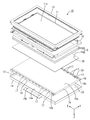
- FIG. 3 is an exploded perspective view showing a relationship among a chassis, a light guide member, and an optical member constituting a backlight device included in the liquid crystal display device.
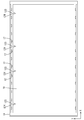
- the top view which shows the state which accommodated the light guide member and the LED board in the chassis which comprises a backlight apparatus.
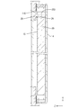
- V-v sectional view of FIG. Vi-vi cross-sectional view of FIG. Sectional view taken along line vii-vii in FIG.
- An enlarged plan view showing a detailed positional relationship among the LED, the light guide member (insertion recess), and the positioning portion.
- the enlarged plan view which shows detailed positional relationship with LED which concerns on the modification 1 of Embodiment 1, a light guide member (insertion recessed part), and a positioning part.
- the enlarged plan view which shows detailed positional relationship with LED which concerns on the modification 2 of Embodiment 1, a light guide member (insertion recessed part), and a positioning part.
- the enlarged plan view which shows detailed positional relationship with LED which concerns on the modification 3 of Embodiment 1, a light guide member (insertion recessed part), and a positioning part.
- the enlarged plan view which shows detailed positional relationship with LED which concerns on the modification 4 of Embodiment 1, light guide member (insertion recessed part), and a positioning part.
- the enlarged plan view which shows detailed positional relationship with LED which concerns on the modification 5 of Embodiment 1, a light guide member (insertion recessed part), and a positioning part.
- the top view which shows the state which accommodated the light guide member and the LED board in the chassis which comprises the backlight apparatus which concerns on Embodiment 2 of this invention.
- Sectional drawing which shows the cross-sectional structure along the short side direction of the liquid crystal display device which concerns on Embodiment 3 of this invention.
- the top view which shows the state which accommodated the light guide member and the LED board in the chassis which comprises the backlight apparatus which concerns on Embodiment 4 of this invention.
- the top view which shows the state which accommodated the light guide member and the LED board in the chassis which comprises the backlight apparatus which concerns on other embodiment (1) of this invention.
- Sectional drawing which shows the cross-sectional structure along the short side direction of the liquid crystal display device which concerns on other embodiment (2) of this invention.
- FIGS. 1 A first embodiment of the present invention will be described with reference to FIGS.
- the liquid crystal display device 10 is illustrated.
- a part of each drawing shows an X axis, a Y axis, and a Z axis
- each axis direction is drawn to be a direction shown in each drawing.
- the Y-axis direction coincides with the vertical direction
- the X-axis direction coincides with the horizontal direction.
- the vertical direction is used as a reference for upper and lower descriptions.
- the upper side shown in FIG. 2 be a front side
- the lower side of the figure be a back side.
- the television receiver TV includes a liquid crystal display device 10, front and back cabinets Ca and Cb that are accommodated so as to sandwich the liquid crystal display device 10, a power source P, a tuner T, And a stand S.
- the liquid crystal display device (display device) 10 has a horizontally long (longitudinal) rectangular shape (rectangular shape) as a whole, and is housed in a vertically placed state so that its display surface 11a is along the vertical direction (Y-axis direction).
- the liquid crystal display device 10 includes a liquid crystal panel 11 that is a display panel and a backlight device (illumination device) 12 that is an external light source, which are integrated by a frame-like bezel 13 or the like. Is supposed to be retained.
- the phrase “the display surface 11a of the liquid crystal panel 11 is along the vertical direction” as referred to in the present embodiment is not limited to an aspect in which the display surface 11a of the liquid crystal panel 11 is parallel to the vertical direction, but from a direction along the horizontal direction. Also, it means that it is installed in a direction relatively along the vertical direction, and includes, for example, those inclined by 0 ° to 45 °, preferably 0 ° to 30 ° with respect to the vertical direction.
- the liquid crystal panel 11 has a horizontally long (longitudinal) rectangular shape (rectangular shape) in a plan view, and a pair of glass substrates are bonded together with a predetermined gap therebetween, The liquid crystal is sealed between both glass substrates.
- One glass substrate is provided with a switching element (for example, TFT) connected to a source wiring and a gate wiring orthogonal to each other, a pixel electrode connected to the switching element, an alignment film, and the like.
- the substrate is provided with a color filter and counter electrodes in which colored portions such as R (red), G (green), and B (blue) are arranged in a predetermined arrangement, and an alignment film.
- a polarizing plate is disposed on the outside of both substrates.
- the backlight device 12 covers a substantially box-shaped chassis 14 having an opening that opens toward the light emission surface side (the liquid crystal panel 11 side), and covers the opening of the chassis 14.
- the optical member 15 group (diffusing plate (light diffusing member) 15a and a plurality of optical sheets 15b arranged between the diffusing plate 15a and the liquid crystal panel 11) is provided.
- an LED 17 Light Emitting Diode
- an LED substrate 18 on which the LED 17 is surface-mounted, and light from the LED 17 are guided to the optical member 15 (liquid crystal panel 11).
- a frame 16 capable of pressing the light guide member 19 from the front side.
- the backlight device 12 includes an LED board 18 having LEDs 17 at both upper and lower ends (long-side ends) in the vertical direction, and a vertical center between the LED boards 18. It is a so-called edge light type (side light type) in which the light guide member 19 is disposed. Below, each component of the backlight apparatus 12 is demonstrated in detail.
- the chassis 14 is made of metal, and as shown in FIGS. 2 and 3, a pair of a bottom plate 14a having a horizontally long rectangular shape as in the liquid crystal panel 11 and a pair of rising edges from both outer ends on the long side of the bottom plate 14a. It consists of a side plate 14b.
- the long side direction of the chassis 14 (bottom plate 14a) coincides with the X-axis direction (horizontal direction), and the short side direction coincides with the Y-axis direction (vertical direction).
- the frame 16 and the bezel 13 can be screwed to the side plate 14b.
- the optical member 15 has a horizontally long rectangular shape when viewed in a plane, like the liquid crystal panel 11 and the chassis 14.
- the optical member 15 is placed on the front side (light emitting side) of the light guide member 19 and is disposed between the liquid crystal panel 11 and the light guide member 19.
- the optical member 15 includes a diffusion plate 15a disposed on the back side (light guide member 19 side, opposite to the light emitting side) and an optical sheet 15b disposed on the front side (liquid crystal panel 11 side, light emitting side). Composed.
- the diffusing plate 15a has a structure in which a large number of diffusing particles are dispersed in a substantially transparent resin-made base material having a predetermined thickness, and has a function of diffusing transmitted light.
- the optical sheet 15b has a sheet shape that is thinner than the diffusion plate 15a, and three optical sheets are laminated.
- Specific types of the optical sheet 15b include, for example, a diffusion sheet, a lens sheet, a reflective polarizing sheet, and the like, which can be appropriately selected and used. 3 and 5 to 7, the illustration of the optical member 15 is simplified. Specifically, the optical member 15 composed of a plurality of (four) sheets is collectively shown as one sheet. .
- the frame 16 is formed in a frame shape (frame shape) extending along the outer peripheral end portion of the light guide member 19, and the outer peripheral end portion of the light guide member 19 extends over substantially the entire circumference. It can be pressed from the front side.
- the frame 16 is made of a synthetic resin and has a light shielding property by having a surface with, for example, a black color.
- first reflective sheets 20 that reflect light are respectively provided on the back side surfaces of both long side portions of the frame 16, that is, the surfaces facing the light guide member 19 and the LED substrate 18 (LED 17). It is attached.
- the first reflection sheet 20 has a size that extends over substantially the entire length of the long side portion of the frame 16, and is in direct contact with the end portion of the light guide member 19 on the LED 17 side and the light guide member 19.
- the end portion and the LED substrate 18 are collectively covered from the front side.
- the frame 16 can receive the outer peripheral end of the liquid crystal panel 11 from the back side.
- the LED 17 has a structure in which an LED chip is sealed with a resin material on a substrate portion fixed to the LED substrate 18, as shown in FIGS.
- the LED chip mounted on the substrate unit has one main emission wavelength, and specifically, one that emits blue light in a single color is used.
- the resin material that seals the LED chip is dispersed and blended with a phosphor that emits a predetermined color when excited by the blue light emitted from the LED chip, and generally emits white light as a whole. It is said.
- the phosphor for example, a yellow phosphor that emits yellow light, a green phosphor that emits green light, and a red phosphor that emits red light are used in appropriate combination, or any one of them is used.
- the LED 17 is a so-called top type in which a surface opposite to the mounting surface with respect to the LED substrate 18 is a light emitting surface.
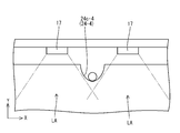
- the light emitted from the LED 17 spreads radially within a predetermined angular range around the optical axis A indicated by the two-dot chain line in FIG. 8, and the irradiation area LA sandwiches the optical axis A in FIG. It is set as the area
- the dashed-dotted line in FIG. 8 has shown the outermost position of irradiation area LA.
- the LED board 18 is made of synthetic resin (epoxy resin or the like) or ceramic, and as shown in FIGS. 2 and 4, the long side direction of the chassis 14 (the end of the light guide member 19 on the LED 17 side, the X-axis direction). , Extending in the horizontal direction), and having a main plate surface parallel to the X-axis direction and the Z-axis direction, that is, the liquid crystal panel 11 and the light guide member 19 (optical member 15). ) In a posture orthogonal to the plate surface.
- the LED board 18 has a posture in which the long side direction on the main plate surface coincides with the X-axis direction, the short side direction coincides with the Z-axis direction, and the plate thickness direction orthogonal to the main plate surface coincides with the Y-axis direction. It is said.
- the LED board 18 is disposed at both upper and lower ends in the vertical direction (Y-axis direction) so as to sandwich the light guide member 19 in the chassis 14. Are attached by screws or the like to the long side plate 14b.
- a plurality (13 in FIG. 2) of LEDs 17 are arranged in the long side direction of the LED substrate 18 (light guide member). 19 at the end of the LED 17 side, the X-axis direction, and the horizontal direction). The interval between the LEDs 17 adjacent to each other in the X-axis direction, that is, the arrangement pitch of the LEDs 17 is substantially equal.
- the pair of LED boards 18 arranged at the upper and lower ends in the vertical direction are housed in the chassis 14 with the mounting surfaces of the LEDs 17 facing each other, and thus the light emitting surfaces of the LEDs 17 mounted on the LED boards 18 respectively.
- the optical axis of each LED 17 substantially coincides with the vertical direction (Y-axis direction).
- the LEDs 17 mounted on the pair of LED substrates 18 are respectively arranged so as to be opposed to the vertical upper and lower end portions (long side end portions) of the light guide member 19.
- a raw material used for the LED board 18 it is also possible to set it as the structure which used metal materials, such as the same aluminum type material as the chassis 14, for example, and formed the wiring pattern on the surface through the insulating layer.
- the light guide member 19 is made of a synthetic resin material (for example, acrylic) having a refractive index higher than that of air and substantially transparent (excellent translucency). As shown in FIG. 2, the light guide member 19 is formed in a plate shape having a horizontally long rectangular shape when seen in a plan view like the liquid crystal panel 11 and the chassis 14, and the long side direction on the main plate surface is the X-axis direction. (Horizontal direction, LED 17 parallel direction) and the short side direction coincide with the Y-axis direction (vertical direction), respectively, and the plate thickness direction perpendicular to the main plate surface coincides with the Z-axis direction. As shown in FIG.
- the light guide member 19 is disposed in the chassis 14 immediately below the liquid crystal panel 11 and the optical member 15, and a pair of LED substrates disposed at both upper and lower ends in the vertical direction of the chassis 14. It is arranged in a form sandwiched between 18 in the vertical direction. Therefore, the alignment direction of the LED 17 (LED substrate 18) and the light guide member 19 matches the Y-axis direction (vertical direction), whereas the alignment direction of the optical member 15 (liquid crystal panel 11) and the light guide member 19 Is coincident with the Z-axis direction, and both alignment directions are orthogonal to each other.
- the light guide member 19 introduces light emitted from the LED 17 in the Y-axis direction, and rises and emits the light toward the optical member 15 side (Z-axis direction) while propagating the light inside. It has a function. Note that the light guide member 19 is substantially the same size as the optical member 15 described above in plan view, and the outer peripheral end thereof is indirectly pressed by the frame 16 from the front side via the optical member 15.
- the surface facing the front side (the surface covered by the optical member 15) emits light from the inside toward the optical member 15 and the liquid crystal panel 11 as shown in FIG. 3. It becomes the surface 19a.
- the optical member 15 is disposed between the light emitting surface 19 a of the light guide member 19 and the liquid crystal panel 11.
- the upper and lower end surfaces in the vertical direction are respectively LEDs 17 (LED substrates 18). And are opposed to each other at a predetermined interval, and these constitute a light incident surface 19b on which light emitted from the LED 17 is incident.
- the first reflection sheet 20 described above is arranged, whereas on the back side of the space, The second reflection sheet 21 is disposed so as to sandwich the same space with the first reflection sheet 20.
- Both reflection sheets 20 and 21 are arranged so as to sandwich the LED 17 side end portion of the light guide member 19 and the LED 17 in addition to the above space. Thereby, the light from LED17 can be made to inject efficiently with respect to the light-incidence surface 19b by repeatedly reflecting between both the reflective sheets 20 and 21.
- the light incident surface 19b is a surface parallel to the X-axis direction and the Z-axis direction (the main plate surface of the LED substrate 18), and is a surface substantially orthogonal to the light emitting surface 19a. Further, the alignment direction of the LED 17 and the light incident surface 19b coincides with the Y-axis direction (vertical direction) and is parallel to the light emitting surface 19a.
- a light guide reflection sheet 22 that can reflect the light in the light guide member 19 and rise up to the front side covers the entire area.
- the light guide reflection sheet 22 is disposed between the bottom plate 14 a of the chassis 14 and the light guide member 19.
- the light guide reflection sheet 22 has a reflecting portion (not shown) that reflects internal light or a scattering portion that scatters internal light (see FIG. (Not shown) is patterned so as to have a predetermined in-plane distribution, and thereby, the emitted light from the light emitting surface 19a is controlled to have a uniform distribution in the surface.
- a positioning portion 23 for positioning the light guide member 19 is provided in the chassis 14, and an insertion recess 24 through which the positioning portion 23 is inserted is provided in the light guide member 19.
- the light guide member 19 is positioned with respect to the chassis 14 and the LED 17 (LED board 18) fixed to the chassis 14 in the direction along the main plate surface (plane direction), that is, the X-axis direction and the Y-axis direction. It is possible to do.
- the light guide member 19 is formed by cutting out the insertion recess 24, there is a concern that the insertion recess 24 may adversely affect the light propagating in the light guide member 19.
- the insertion recess 24 is tapered toward the direction away from the LED 17.
- the insertion recess 24 and the positioning portion 23 will be described in detail in order.
- the insertion recess 24 is provided in the short side direction of the light guide member 19, that is, the upper end portion in the vertical direction (Y-axis direction) (the upper end portion in FIG. 4).
- a pair of insertion recesses 24 are arranged on both ends of the light guide member 19 in the long side direction (X-axis direction, LED 17 parallel direction).
- the distance (interval) between the pair of insertion recesses 24 is slightly smaller than the long side dimension of the light guide member 19, but is much larger than the interval between the LEDs 17 adjacent in the X-axis direction (arrangement pitch of the LEDs 17). It is supposed to be. That is, it can be said that the insertion recess 24 is arranged to be sparser than the LED 17.
- Each insertion recessed part 24 is distribute
- the insertion recess 24 is arranged at a position deviated (offset) in the X-axis direction (parallel direction of the LED 17) with respect to the LED 17, and is arranged in a non-facing arrangement, or in other words, in an obliquely arranged arrangement.
- the insertion recess 24 penetrates the light guide member 19 in the plate thickness direction (Z-axis direction) at the upper end portion in the vertical direction of the light guide member 19 and is located on the upper side in the vertical direction (Y-axis direction) ( 4 and FIG. 7), that is, the LED 17 is opened.
- the insertion recess 24 has a triangular shape in plan view, and the opening width to the LED 17 side (dimension in the X-axis direction) is the lower side in the vertical direction, that is, the direction away from the LED 17. It is set as the form which becomes small gradually continuously toward this.
- the insertion recess 24 is formed by partially cutting out the upper end portion (light incident surface 19b) in the vertical direction of the light guide member 19 into a V-shaped groove.
- the insertion recess 24 has an isosceles triangle shape when seen in a plan view, and has a line-symmetric shape with respect to a symmetry line along the Y-axis direction passing through an intermediate position between adjacent LEDs 17. Accordingly, the pair of side surfaces (interfaces) 24a included in the insertion recess 24 is inclined with respect to the Y-axis direction, that is, the optical axis A of the LED 17 (the alignment direction of the LED 17 and the light guide member 19). The angles are assumed to be equal to each other.
- a side surface 24a of the insertion recess 24 is an interface with an external air layer.
- the side surface 24a of the insertion recess 24 is arranged so as not to overlap with the irradiation area LA of each LED 17 adjacent to the insertion recess 24 (a chain line in FIG. 8).
- the insertion recess 24 is arranged so that the entire region thereof exists in the non-irradiation region NLA that is out of the irradiation region LA of the adjacent LEDs 17 across the insertion recess 24.
- the side surface 24a of the insertion recess 24 is inclined with respect to the optical axis A of the LED 17, and the inclination angle is such that the one-dot chain line indicating the outermost position of the irradiation area LA in FIG.
- the “non-irradiation region NLA of the LED 17” referred to here is a region deviated from any of the irradiation regions LA of the respective LEDs 17, and in FIG. 8, a pair of alternate long and short dashed lines (of the irradiation region LA) A substantially V-shaped region between the outermost positions).
- the angle range of the non-irradiation region NLA having a substantially V shape is wider than the angle range of the insertion recess 24 having a V shape.
- the positioning portion 23 is a position aligned with each insertion recess 24 of the light guide member 19 in the bottom plate 14 a of the chassis 14, that is, an upper end portion in the vertical direction and both ends in the X-axis direction. A pair is arranged at a position to be closer.
- the positioning portion 23 has a substantially columnar shape protruding from the bottom plate 14a toward the front side along the Z-axis direction, and the protruding dimension is equal to the plate thickness dimension of the light guide member 19 and the optical dimension as shown in FIG.
- the size of the member 15 is larger than the sum of the plate thickness dimensions. As shown in FIG.
- the positioning portion 23 is fixed to the chassis 14 and the chassis 14 in the X-axis direction and the Y-axis direction by being inserted into the insertion recess 24 and abutting against the side surface 24a.
- the light guide member 19 can be positioned with respect to the LED 17.
- the positioning portion 23 and the insertion recess 24 form a pair and are disposed at both ends in the long side direction of the light guide member 19, the light guide member 19 can be accurately positioned and the light guide member 19. It is also possible to prevent the rotation.
- the diameter of the positioning portion 23 is smaller than the maximum opening width of the insertion recess 24 toward the LED 17 (opening width at the upper end position in the vertical direction of the light guide member 19).
- the positioning portion 23 is integrally formed with the bottom plate 14 a of the chassis 14.
- the optical member 15 stacked on the light emitting side with respect to the light guide member 19 is connected to the above-described insertion recess 24 and the second insertion recess through which the positioning portion 23 is inserted. 25, so that the optical member 15 can be positioned with respect to the chassis 14 and the LED 17 together with the light guide member 19 in the direction along the main plate surface (plane direction), that is, in the X-axis direction and the Y-axis direction. It is said that.
- the second insertion recess 25 is paired at a position in the optical member 15 that is aligned with the two sets of insertion recesses 24 and the positioning portion 23, that is, at a position at the upper end in the vertical direction and closer to both ends in the X-axis direction. It is arranged.
- the second insertion recess 25 has a hole shape that penetrates the optical member 15 in the plate thickness direction (Z-axis direction), opens only in the Z-axis direction, and is in the X-axis direction and the Y-axis direction. It is set as the form which does not open in a direction.
- the second insertion recess 25 has a substantially circular shape in plan view following the outer shape of the positioning portion 23, and the diameter of the second insertion recess 25 is slightly larger than the diameter of the positioning portion 23. Insertion is possible.
- the hole edge of the second insertion recess 25 can be brought into contact with the outer surface of the positioning portion 23 as shown in FIG. 7. If the plate surface of the optical member 15 is in a posture along the vertical direction, the edge of the second insertion recess 25 can be supported by the positioning portion 23 in the vertical direction. In other words, since the optical member 15 can be supported in a suspended state in the vertical direction by the positioning portion 23, it is possible to prevent the optical member 15 from being deformed such as wrinkles or deflection due to its own weight.
- the second insertion recess 25 is formed at the upper end of the optical member 15 in the vertical direction, and the upper end can be supported by being suspended by the positioning portion 23.
- the second insertion recesses 25 described above are formed in all of the diffusion plate 15a and the optical sheet 15b included in the optical member 15, and the second insertion recesses 25 formed in the optical members 15 are mutually connected. Is matched (communication).
- the light guide reflection sheet 22 attached to the surface 19c of the light guide member 19 opposite to the light exit surface 19a protrudes from the bottom plate 14a toward the light guide member 19 as shown in FIG.
- An insertion hole 26 through which the positioning portion 23 is inserted is formed.
- a pair of insertion holes 26 are arranged at positions in the light guide reflection sheet 22 that are aligned with the pair of insertion recesses 24, that is, at positions that are upper end portions in the vertical direction and closer to both ends in the X-axis direction.
- the insertion hole 26 has a hole shape that penetrates the light guide reflection sheet 22 in the plate thickness direction (Z-axis direction), like the second insertion recess 25, and opens only in the Z-axis direction.
- the insertion hole 26 has a substantially circular shape in plan view, following the outer shape of the positioning portion 23, and its diameter is slightly larger than the diameter of the positioning portion 23.
- the positioning part 23 can be inserted.
- This embodiment has the structure as described above, and its operation will be described next.
- the separately manufactured liquid crystal panel 11, backlight device 12, bezel 13 and the like are assembled.
- a manufacturing procedure of the liquid crystal display device 10 will be described.
- the light guide reflection sheet 22 is integrally attached to the light guide member 19 in advance, and the insertion hole 26 and the insertion recess 24 are aligned with each other.
- the pair of insertion recesses 24 insertion holes 26
- the positioning portions 23 are inserted into the corresponding insertion holes 26 and the insertion recesses 24.
- the positioning portion 23 is in a state of penetrating the light guide member 19 and the front end portion protruding to the front side of the light guide member 19 (FIG. 7).
- an operation of stacking the optical member 15 on the light emitting surface 19a of the light guide member 19 is performed.
- the optical member 15 is laminated on the light emitting surface 19a of the light guide member 19 in the order of the diffusion plate 15a and the optical sheet 15b (diffusion sheet, lens sheet, reflective polarizing sheet).
- the second insertion recesses 25 formed in the optical members 15 are aligned with the pair of positioning portions 23. As the optical member 15 is stacked on the light guide member 19, each positioning portion 23 is inserted into each second insertion recess 25.
- the optical member 15 is positioned with respect to the light guide member 19 and the chassis 14 in the direction along the main plate surface (plane direction), that is, the X-axis direction and the Y-axis direction.
- the second insertion recess 25 is also aligned with the insertion recess 24 and the insertion hole 26.
- the frame 16 is attached to the chassis 14, and then the liquid crystal panel 11 and the bezel 13 are assembled in this order, whereby the liquid crystal display device 10 is obtained.
- the driving of the liquid crystal panel 11 is controlled by a control circuit (not shown), and the driving power from a power supply board (not shown) is supplied to each LED 17 on the LED board 18.
- the drive is controlled by being supplied to.
- the light from each LED 17 is guided by the light guide member 19, so that the liquid crystal panel 11 is irradiated through the optical member 15, and a predetermined image is displayed on the liquid crystal panel 11.
- the operation of the backlight device 12 will be described in detail.
- the space is optically closed by the first reflective sheet 20 on the front side and the second reflective sheet 21 on the back side. Therefore, the light from the LED 17 is repeatedly reflected by both the reflection sheets 20 and 21, so that it is efficiently incident on the light incident surface 19b without leaking to the outside.
- the incident efficiency of light from each LED 17 with respect to the light guide member 19 depends on the positional relationship between the LED 17 and the light incident surface 19b, and when the positional relationship changes, the incident efficiency may also change. Is done.
- the light guide member 19 is positioned with respect to the chassis 14 in the X-axis direction and the Y-axis direction by the positioning unit 23, and therefore, the light guide member 19 is an LED fixed to the chassis 14. It is also indirectly positioned with respect to each LED 17 on the substrate 18. As a result, the positional relationship between each LED 17 and the light incident surface 19b in the X-axis direction and the Y-axis direction is maintained constant, and the light incident efficiency from each LED 17 becomes stable, thereby suppressing luminance unevenness. Preferred.
- the insertion recess 24 formed in the light guide member 19 is tapered toward the direction away from the LED 17 as shown in FIG. It is arranged at a position that is out of the direction, that is, a position that is not directly facing.
- the insertion recess 24 has a whole area within the non-irradiation region NLA of the LED 17 and a shape following the non-irradiation region NLA having a substantially V shape, that is, a triangular shape in plan view.
- the insertion recess enters the irradiation area LA of the LED 17, so that the light from the LED 17 easily enters the insertion recess, thereby guiding the light.
- the distribution of light propagating in the member 19 is biased to cause a partial dark portion.
- the insertion recess is disposed at a position facing the LED 17, light from the LED 17 directly enters the insertion recess, so that the distribution of light propagating in the light guide member 19 is largely biased. May occur.
- the insertion recess 24 since the insertion recess 24 has the above-described configuration and arrangement, it is difficult for light from the LED 17 to enter the insertion recess 24, and thereby the distribution of light propagating in the light guide member 19. Bias is not likely to occur and is uniform. Therefore, it is possible to prevent a partial dark portion from being generated in the light guide member 19, and thus it is possible to suppress the occurrence of uneven brightness in the light emitted from the light exit surface 19a.
- the non-irradiation area NLA can be maintained as before, it is not necessary to widen the interval between the adjacent LEDs 17, whereby the installation density of the LEDs 17 can be kept high, which is suitable for increasing the brightness.
- the insertion recesses 24 that can cause dark portions are arranged on both ends of the light guide member 19 in the X-axis direction, luminance unevenness is less likely to occur compared to a case where the insertion recesses 24 are arranged on the center side.
- each LED 17 in the backlight device 12 is turned on or off, so that a change occurs in the internal temperature environment.
- Each component can expand or contract thermally.
- the positioning portion 23 is inserted into the second insertion recess 25 formed at the upper end of the optical member 15 in the vertical direction, and the hole edge of the second insertion recess 25 is supported in the vertical direction by the positioning portion 23.
- the optical member 15 since the optical member 15 is supported in a suspended state, even when the optical member 15 expands or contracts due to thermal expansion or thermal contraction, the optical member 15 itself has its own weight to substantially It is possible to prevent deformation such as wrinkling and bending over the entire area. Thereby, it is possible to prevent the occurrence of luminance unevenness due to the thermal expansion or contraction of the optical member 15 in advance.
- the backlight device 12 includes the LED 17 that is a light source, the light guide member 19 in which the LED 17 is arranged to face the end, and the light guide member 19 in the surface direction.
- the light guide member 19 can be positioned in the surface direction by inserting the positioning portion 23 into the insertion recess 24 formed in the light guide member 19.
- the positional relationship between the light guide member 19 and the LED 17 can be kept constant, so that the incident efficiency of light incident on the light guide member 19 from the LED 17 can be stabilized, thereby suppressing luminance unevenness. It becomes suitable for.
- the insertion recess 24 formed at the end of the light guide member 19 on the LED 17 side is tapered toward the direction away from the LED 17, so that the insertion recess has a constant width.
- the light which injected into the edge part of the light guide member 19 from LED17 becomes difficult to approach into the penetration recessed part 24.
- FIG. if the light incident on the end portion of the light guide member 19 from the LED 17 goes into the insertion recess 24, the light is reflected (including total reflection) or refracted at the interface of the insertion recess 24.
- the distribution of the light propagating in the light 19 is biased and becomes non-uniform. For example, a part of the light guide member 19 locally becomes a dark part with a small amount of light, and as a result, there is a risk of uneven brightness.
- the light incident on the end portion of the light guide member 19 from the LED 17 is difficult to enter the insertion recess 24, and thus the light distribution propagating in the light guide member 19 is biased. Therefore, it is possible to prevent dark portions, that is, uneven brightness from occurring in the light guide member 19.
- a plurality of LEDs 17 are intermittently arranged in parallel along the end of the light guide member 19, and the positioning portion 23 and the insertion recess 24 are arranged at a position away from the LED 17 in the parallel direction of the LEDs 17. ing. If it does in this way, the light from LED17 in which a plurality will be intermittently arranged in parallel along the edge part in the edge part of light guide member 19 will enter efficiently. Since the positioning portion 23 and the insertion recess 24 are arranged at a position deviated from the LED 17 in the parallel direction of the LED 17, it becomes difficult for light from the LED 17 to enter the insertion recess 24, thereby suitably suppressing luminance unevenness. can do.
- the positioning part 23 and the insertion recessed part 24 are distribute
- the positioning part 23 and the insertion recessed part 24 are arrange
- the insertion recess 24 is tapered, light from the LED 17 is inserted even if the interval between the adjacent LEDs 17 is narrower than when the insertion recess has a constant width. A state where it is difficult to enter the recess 24 can be maintained. Since the installation density of the LEDs 17 can be increased by narrowing the interval between the LEDs 17, it is possible to increase the brightness.
- the distances between the adjacent LEDs 17 and the positioning portion 23 and the insertion recess 24 arranged therebetween are equal. In this way, it becomes difficult for the light from the adjacent LEDs 17 to enter the insertion recesses 24 disposed between them, which is more suitable for suppressing luminance unevenness.
- the insertion recess 24 has a line-symmetric shape with respect to a symmetry line passing through an intermediate position between the adjacent LEDs 17. If it does in this way, the positional relationship of adjacent LED17 with respect to the interface of the insertion recessed part 24 will become equivalent by making the insertion recessed part 24 into a line symmetrical shape. Thereby, it becomes more suitable for suppression of luminance unevenness.
- a plurality of positioning portions 23 and insertion recesses 24 are provided in pairs, and the interval between adjacent positioning portions 23 and insertion recesses 24 is larger than the interval between adjacent LEDs 17. It is said. By doing so, the positioning of the light guide member 19 becomes more reliable by providing a plurality of sets of positioning portions 23 and insertion recesses 24.
- the insertion concave portion 24 and the positioning portion 23 that can cause a dark portion are arranged more sparsely than the LED 17, it is more suitable for suppressing luminance unevenness.
- the insertion recess 24 is arranged on the end side in the light guide member 19 in the parallel direction of the LEDs 17. In this way, since the insertion concave portion 24 that may cause a dark portion is arranged on the end side in the parallel direction of the LED 17, brightness unevenness is compared with the case where the insertion concave portion is arranged on the center side in the parallel direction of the LED 17. It becomes more suitable for suppression.
- the insertion recessed part 24 is each distribute
- an optical member 15 that covers the light emitting surface of the light guide member 19 is provided, and the optical member 15 is formed with a second insertion recess 25 that communicates with the insertion recess 24 and that passes through the positioning portion 23. .
- the positioning of the optical member 15 together with the light guide member 19 can be achieved by inserting the positioning portion 23 into the insertion recess 24 and the second insertion recess 25.
- the second insertion recess 25 has a hole shape penetrating the optical member 15 in the plate thickness direction, and the edge of the hole can be supported in the vertical direction by the positioning portion 23. In this way, when the positioning portion 23 is inserted into the second insertion recess 25, the hole edge of the second insertion recess 25 is supported in the vertical direction by the positioning portion 23. That is, since the optical member 15 can be suspended and supported by the positioning unit 23, for example, even when the optical member 15 undergoes thermal expansion or contraction, wrinkles or deflection due to the weight of the optical member 15 itself. It is assumed that the deformation of is difficult to occur. Accordingly, luminance unevenness can be more effectively suppressed.
- the second insertion recess 25 is formed at the upper end of the optical member 15 in the vertical direction. In this way, the upper end portion in the vertical direction of the optical member 15 can be suspended and supported by the positioning portion 23, so that the optical member 15 is unlikely to be deformed such as wrinkles or deflections in the entire vertical region. Therefore, it is more suitable for suppressing luminance unevenness.
- the LEDs 17 are arranged in opposed relation to the upper end portion in the vertical direction and the lower end portion in the vertical direction of the light guide member 19, respectively. In this way, high brightness can be achieved by arranging the LEDs 17 so as to be opposed to the upper and lower ends in the vertical direction. In other words, even when the backlight device 12 is enlarged, sufficient luminance can be obtained, which is suitable for enlargement.
- the insertion recess 24 is configured to open toward the LED 17 side. In this way, it is easier to insert the positioning portion 23 into the insertion recess 24 than in the case where the insertion recess has a hole shape that is closed over the entire circumference, so that the assembly workability is excellent.
- the insertion recess 24 is configured such that the opening width toward the LED 17 side becomes gradually smaller toward the direction away from the LED 17. In this way, the light from the LED 17 is more difficult to enter the insertion recess 24.
- the insertion recess 24 has a triangular shape as viewed in a plane. In this way, the interface of the insertion recess 24 is inclined with respect to the alignment direction of the LED 17 and the light guide member 19, so that the light from the LED 17 is less likely to enter the insertion recess 24.
- the insertion recess 24 has an isosceles triangle shape when viewed in a plane. In this way, the insertion recess 24 has a symmetrical shape, which is suitable when, for example, two LEDs 17 are arranged at a position sandwiching the insertion recess 24.
- the insertion recess 24 is configured to penetrate the light guide member 19 in the plate thickness direction. In this way, the insertion recess 24 can be easily formed in the light guide member 19, which is excellent in manufacturing the light guide member 19.
- a chassis 14 that houses the LEDs 17 and the light guide member 19 is provided, and the positioning portion 23 is formed integrally with the chassis 14. In this way, since the light guide member 19 is positioned by the positioning portion 23 formed integrally with the chassis 14 that houses the LED 17 and the light guide member 19, the positional relationship between the LED 17 and the light guide member 19 is in an appropriate state. Can be kept in.
- the positioning part 23 has a cylindrical shape. If it does in this way, the operation
- a light guide reflection sheet 22 that is a reflection member that covers a surface of the light guide member 19 opposite to the light emitting side is provided.
- the light guide reflection sheet 22 communicates with the insertion recess 24 and is positioned.
- An insertion hole 26 through which 23 is inserted is formed. In this way, the light propagating through the light guide member 19 can be reflected by the light guide reflection sheet 22 toward the light emitting side, and the light can be efficiently emitted from the light guide member 19.
- the light guide reflection sheet 22 can be positioned together with the light guide member 19.
- an LED substrate 18 on which a plurality of LEDs 17 are mounted is provided. If it does in this way, installation of LED17, wiring concerning LED17, etc. can be made simple.
- the light source is an LED 17. In this way, high brightness and low power consumption can be achieved.
- Embodiment 1 of this invention was shown, this invention is not restricted to the said embodiment, For example, the following modifications can also be included.
- members similar to those in the above embodiment are denoted by the same reference numerals as those in the above embodiment, and illustration and description thereof may be omitted.
- the insertion recess 24-1 has a triangular shape when seen in a plan view, and the side surface 24 a-1 indicates the outermost position of the irradiation area LA of the LED 17. Are substantially coincident and parallel to each other. Even with such a configuration, it is possible to make it difficult for light from the LED 17 to enter the insertion recess 24-1.
- the insertion recess 24-2 has a trapezoidal shape when seen in a plane.
- the insertion recess 24-2 connects a pair of side surfaces 24a-2 that are inclined with respect to both the Y-axis direction and the X-axis direction, and ends opposite to the LED 17 side of both side surfaces 24a-2 and the X-axis. And a side surface 24b parallel to the direction. Even with such a configuration, it is difficult for light from the LED 17 to enter the insertion recess 24-2.
- the insertion recess 24-2 has a trapezoidal shape when seen in a plane.
- the side surface 24a-2 (interface) of the insertion recess 24-2 includes a portion that is inclined with respect to the direction in which the LED 17 and the light guide member 19 are arranged, so that light from the LED 17 is inserted. It becomes difficult to enter into the recess 24-2.
- the insertion recess 24-3 has a semicircular shape when viewed in plan.
- the insertion recess 24-3 is formed in an arc shape in which the side surface 24c has a constant curvature over the entire region.
- the opening width to the LED 17 side in the insertion recess 24-3 is equal to the diameter of the circle forming the insertion recess 24-3. Even with such a configuration, it is difficult for light from the LED 17 to enter the insertion recess 24-3.
- the insertion recess 24-3 has a substantially semicircular shape when viewed in plan.
- the side surface 24c (interface) of the insertion recess 24-3 has an arc shape, so that the light from the LED 17 is less likely to enter the insertion recess 24-3.
- the insertion recess 24-4 has a semi-elliptical shape when viewed in plan.
- the insertion recess 24-4 has a configuration in which an ellipse in which the major axis direction coincides with the Y-axis direction and the minor axis direction coincides with the X-axis direction is divided in half along the minor axis direction.
- the opening width to the LED 17 side in the insertion recess 24-4 is equal to the minor axis dimension of the ellipse forming the insertion recess 24-4. Even with such a configuration, it is difficult for light from the LED 17 to enter the insertion recess 24-4.
- the shape of the side surface is optimized according to the positional relationship with the LED 17 (irradiation area LA) by appropriately changing at least one of the major axis dimension and the minor axis dimension of the ellipse forming the insertion recess 24-4. Can be.
- the insertion recess 24-4 has a substantially semi-elliptical shape when viewed in a plane. In this way, the shape of the side surface 24c-4 (interface) of the insertion recess 24-4 can be easily made appropriate in accordance with the positional relationship between the LED 17 and the insertion recess 24-4.
- Modification 5 of Embodiment 1 will be described with reference to FIG. Here, what changed the shape of the insertion recessed part 24-5 is shown.
- the insertion recess 24-5 includes a first part 24 ⁇ / b> A in which the opening width toward the LED 17 side is constant and a second part 24 ⁇ / b> B in which the opening width toward the LED 17 side changes.
- the first part 24A is disposed on the LED 17 side
- the second part 24B is disposed on the opposite side of the LED 17.
- the opening width to the LED 17 side in the first part 24 ⁇ / b> A is substantially the same as the diameter dimension of the positioning part 23.
- the second portion 24B is configured such that the opening width toward the LED 17 side becomes gradually smaller toward the direction away from the LED 17, and is an isosceles triangle shape in plan view. Even with such a configuration, it is difficult for light from the LED 17 to enter the insertion recess 24-5.
- Embodiment 2 A second embodiment of the present invention will be described with reference to FIG. In this Embodiment 2, what changed the installation number of the positioning part 123 and the insertion recessed part 124 is shown. In addition, the overlapping description about the same structure, effect
- the positioning portion 123 and the insertion recess 124 are arranged at positions at predetermined intervals in the X-axis direction at the upper end portion in the vertical direction of the chassis 14 and the light guide member 19. .
- Each positioning part 123 and each insertion recessed part 124 are all arranged at an intermediate position (in a non-irradiation region) between adjacent LEDs 17.
- the number of the positioning portions 123 and the insertion recesses 124 may be set to 5 or more in addition to the illustration, and may be 3 sets.
- Embodiment 3 of the present invention will be described with reference to FIG.
- the positioning portion 223 formed on the frame 116 is shown.
- action, and effect as above-mentioned Embodiment 1 is abbreviate
- the positioning portion 223 is integrally formed with the frame 116 as shown in FIG.
- the positioning portion 223 is configured to protrude from the upper end portion (long side portion) in the vertical direction toward the back side of the frame 116 that forms a frame shape surrounding the outer peripheral end portion of the light guide member 19.
- the positioning portion 223 is sequentially inserted from the front side into the second insertion recess 25 formed in the optical member 15 and the insertion recess 24 formed in the light guide member 19.
- the chassis 14 that houses the LEDs 17 and the light guide member 19 and the frame 116 that is attached to the chassis 14 and can hold the light guide member 19 from the light emitting side are provided.
- the positioning portion 223 is formed integrally with the frame 116. In this way, the light guide member 19 is positioned by the positioning portion 223 formed integrally with the frame 116 attached to the chassis 14 that houses the LED 17 and the light guide member 19. The relationship can be kept in an appropriate state.
- Embodiment 4 A fourth embodiment of the present invention will be described with reference to FIG. In this Embodiment 4, what changed the insertion recessed part 324 is shown. In addition, the overlapping description about the same structure, effect
- a pair of insertion recesses 324 are formed by cutting out the corners at both ends in the X-axis direction among the upper ends of the light guide member 19 in the vertical direction.
- the insertion recess 324 is arranged at a position further away from the LED 17 located at the end of the group of LEDs 17 arranged in parallel in the X-axis direction, closer to the end in the X-axis direction.
- the positioning portion 323 is changed in arrangement in the chassis 14 in correspondence with the insertion recess 324 described above.
- illustration is abbreviate
- the number of LED boards can be three or four, and in addition to the vertical direction, it can be arranged on at least one of the left and right sides in the horizontal direction. Moreover, it is also possible to arrange
- the insertion recess 24 ′ may not penetrate the light guide member 19 in the plate thickness direction.
- the insertion recess 24 ′ has a concave shape that opens only on the front side, that is, on the positioning portion 223 ′ side and the LED 17 side.
- the insertion recess 24 ' has a recess depth that does not overlap the LED 17 in the Z-axis direction. Further, the projecting dimension of the positioning portion 223 ′ from the frame 116 is shorter than that of the third embodiment.
- the LED substrate is disposed on both long sides of the light guide member.
- the LED substrate can be disposed on both short sides of the light guide member. is there. At this time, the number of installed LED boards can be changed to one, and the LED boards can be arranged only on either one of both short sides of the light guide member.
- the insertion recess and the positioning portion are arranged on the end side in the long side direction of the backlight device.
- the present invention also includes a configuration in which the insertion recess) is relatively disposed on the center side in the long side direction.
- the insertion recess and the positioning portion are arranged at the upper end in the vertical direction of the backlight device.
- the insertion recess and the positioning portion (second insertion portion) The present invention includes a configuration in which the concave portion is arranged at the central portion or the lower end portion in the vertical direction.
- the specific shape of the insertion recess can be changed as appropriate.
- the specific shape and size of the positioning portion can be changed as appropriate, and for example, a prismatic shape, a conical shape, and a pyramidal shape can be used.
- the insertion concave portion is open toward the LED side.
- the insertion concave portion does not open toward the LED side, and may be a hole. is there.
- the hole edge of the second insertion recess is shown to have a closed shape (endless annular shape) over the entire circumference, but the hole edge of the second insertion recess is partially opened.
- the shape (end ring) is also included in the present invention.
- the present invention also includes the second insertion recess having a concave shape that does not penetrate the optical member.
- the positioning unit is formed integrally with the chassis or the frame.
- the positioning unit is formed as a separate part from the chassis and the frame, and the positioning unit is formed.
- the present invention includes those in which the frame is integrated with the chassis or frame by a fixing method such as adhesion.
- the optical member is composed of a diffusion plate and three optical sheets.
- the type and number of optical members can be changed as appropriate. .
- the present invention includes an LED using a type of LED in which three types of LED chips each emitting C (cyan), M (magenta), and Y (yellow) are monochromatic.
- the liquid crystal panel is exemplified as a vertically placed state in which the short side direction coincides with the vertical direction, but the liquid crystal panel matches the long side direction with the vertical direction. What is set in a vertical state is also included in the present invention.
- a TFT is used as a switching element of a liquid crystal display device.
- the present invention can also be applied to a liquid crystal display device using a switching element other than TFT (for example, a thin film diode (TFD)).
- a switching element other than TFT for example, a thin film diode (TFD)
- the present invention can also be applied to a liquid crystal display device for monochrome display.
- the liquid crystal display device using the liquid crystal panel is exemplified as the display element.
- the present invention can be applied to display devices using other types of display elements.
- the television receiver provided with the tuner is exemplified.
- the present invention can also be applied to a display device that does not include the tuner.
- SYMBOLS 10 Liquid crystal display device (display device), 11 ... Liquid crystal panel (display panel), 12 ... Backlight device (illumination device), 14 ... Chassis, 15 ... Optical member, 16, 116 ... Frame, 17 ... LED (light source) , 18 ... LED substrate (light source substrate), 19 ... light guide member, 19a ... light emitting surface, 22 ... light guide reflection sheet (reflective member), 23, 123, 223, 323 ... positioning part, 24, 124, 324 ... Insertion recessed part, 24a, 24c ... Side surface (interface), 25 ... 2nd insertion recessed part, 26 ... Insertion hole, TV ... Television receiver
Abstract
Description
しかしながら、上記した特許文献1に記載されたものは、光学部材の直下に光源が配置された、いわゆる直下型のバックライト装置に関するものであり、導光部材を備え且つその端部に光源が配置された、いわゆるエッジライト型のバックライト装置に関しては、その構成を加味した検討が十分に行われていないのが実情であった。
本発明の照明装置は、光源と、前記光源が端部に対して対向状に配される導光部材と、前記導光部材をその面方向について位置決め可能な位置決め部とを備え、前記導光部材における前記光源側の端部には、前記位置決め部を挿通する挿通凹部が形成され、この挿通凹部が前記光源から遠ざかる方向に向けて先細り状をなしている。
(1)前記光源は、前記導光部材の端部に沿って複数が間欠的に並列して配されており、前記位置決め部及び前記挿通凹部は、前記光源の並列方向について前記光源から外れた位置に配されている。このようにすれば、導光部材の端部には、その端部に沿って複数が間欠的に並列して配される光源からの光が効率的に入射される。位置決め部及び挿通凹部が、光源の並列方向について光源から外れた位置に配されているから、光源からの光が挿通凹部内に進入し難いものとなり、それにより輝度ムラを好適に抑制することができる。
本発明によれば、輝度ムラを抑制することができる。
本発明の実施形態1を図1から図8によって説明する。本実施形態では、液晶表示装置10について例示する。なお、各図面の一部にはX軸、Y軸及びZ軸を示しており、各軸方向が各図面で示した方向となるように描かれている。このうちY軸方向は、鉛直方向と一致し、X軸方向は、水平方向と一致している。また、特に断りがない限りは、上下の記載については鉛直方向を基準とする。また、図2に示す上側を表側とし、同図下側を裏側とする。
実施形態1の変形例1について図9を用いて説明する。ここでは、挿通凹部24‐1の形状を変更したものを示す。
実施形態1の変形例2について図10を用いて説明する。ここでは、挿通凹部24‐2の形状を変更したものを示す。
実施形態1の変形例3について図11を用いて説明する。ここでは、挿通凹部24‐3の形状を変更したものを示す。
実施形態1の変形例4について図12を用いて説明する。ここでは、挿通凹部24‐4の形状を変更したものを示す。
実施形態1の変形例5について図13を用いて説明する。ここでは、挿通凹部24‐5の形状を変更したものを示す。
本発明の実施形態2を図14によって説明する。この実施形態2では、位置決め部123及び挿通凹部124の設置数を変更したものを示す。なお、上記した実施形態1と同様の構造、作用及び効果について重複する説明は省略する。
本発明の実施形態3を図15によって説明する。この実施形態3では、位置決め部223をフレーム116に形成したものを示す。なお、上記した実施形態1と同様の構造、作用及び効果について重複する説明は省略する。
本発明の実施形態4を図16によって説明する。この実施形態4では、挿通凹部324を変更したものを示す。なお、上記した実施形態1と同様の構造、作用及び効果について重複する説明は省略する。
本発明は上記記述及び図面によって説明した実施形態に限定されるものではなく、例えば次のような実施形態も本発明の技術的範囲に含まれる。
(1)上記した各実施形態では、LED基板が鉛直方向の上下(両長辺側)に一対配されたものを示したが、LED基板の設置数は適宜に変更可能である。例えば、図17に示すように、LED基板18を鉛直方向の上側にのみ1枚配置し、鉛直方向の下側にはLED基板18を設置しない構成とすることも可能である。このような構成は、特に画面サイズが小型の液晶表示装置(バックライト装置)に好適であり、製造コストの低廉化を図ることができる。なお、図17以外にも、LED基板の設置数を3枚または4枚とし、鉛直方向の上下に加えて、水平方向の左右の少なくともいずれか一方に配置することも可能である。また、LED基板を水平方向の左右にそれぞれ配置することも可能であり、それに加えて鉛直方向の上下の少なくともいずれか一方にLED基板を配置することも可能である。
Claims (29)
- 光源と、
前記光源が端部に対して対向状に配される導光部材と、
前記導光部材をその面方向について位置決め可能な位置決め部とを備え、
前記導光部材における前記光源側の端部には、前記位置決め部を挿通する挿通凹部が形成され、この挿通凹部が前記光源から遠ざかる方向に向けて先細り状をなしている照明装置。 - 前記光源は、前記導光部材の端部に沿って複数が間欠的に並列して配されており、
前記位置決め部及び前記挿通凹部は、前記光源の並列方向について前記光源から外れた位置に配されている請求項1記載の照明装置。 - 前記位置決め部及び前記挿通凹部は、隣り合う前記光源の間に配されている請求項2記載の照明装置。
- 隣り合う各前記光源と、その間に配される前記位置決め部及び前記挿通凹部との距離が等しいものとされる請求項3記載の照明装置。
- 前記挿通凹部は、隣り合う前記光源間の中間位置を通る対称線に関して線対称形状とされる請求項4記載の照明装置。
- 前記位置決め部及び前記挿通凹部は、互いに組をなす形で複数ずつ設けられており、
隣り合う前記位置決め部及び前記挿通凹部の組間の間隔は、隣り合う前記光源間の間隔よりも大きいものとされる請求項2から請求項5のいずれか1項に記載の照明装置。 - 前記挿通凹部は、前記導光部材のうち前記光源の並列方向について端側に配されている請求項2から請求項6のいずれか1項に記載の照明装置。
- 前記挿通凹部は、前記導光部材のうち前記光源の並列方向について両端側にそれぞれ配されている請求項7記載の照明装置。
- 前記導光部材における光出射面を覆う光学部材が備えられており、
前記光学部材には、前記挿通凹部に連通するとともに前記位置決め部を挿通する第2挿通凹部が形成されている請求項1から請求項8のいずれか1項に記載の照明装置。 - 前記第2挿通凹部は、前記光学部材をその板厚方向に貫通する孔状をなしており、その孔縁が前記位置決め部により鉛直方向について支持可能とされる請求項9記載の照明装置。
- 前記第2挿通凹部は、前記光学部材における前記鉛直方向の上端部に形成されている請求項10記載の照明装置。
- 前記光源は、前記導光部材における前記鉛直方向の上端部と、前記鉛直方向の下端部とにそれぞれ対向状に配されている請求項11記載の照明装置。
- 前記挿通凹部は、前記光源側へ向けて開口する形態とされる請求項1から請求項12のいずれか1項に記載の照明装置。
- 前記挿通凹部は、前記光源側への開口幅が、前記光源から遠ざかる方向に向けて連続的に漸次小さくなる形態とされる請求項13記載の照明装置。
- 前記挿通凹部は、平面に視て三角形状をなしている請求項14記載の照明装置。
- 前記挿通凹部は、平面に視て二等辺三角形状をなしている請求項15記載の照明装置。
- 前記挿通凹部は、平面に視て台形状をなしている請求項14記載の照明装置。
- 前記挿通凹部は、平面に視て略半円形状をなしている請求項14記載の照明装置。
- 前記挿通凹部は、平面に視て略半楕円形状をなしている請求項14記載の照明装置。
- 前記挿通凹部は、前記導光部材をその板厚方向に貫通する形態とされる請求項13から請求項19のいずれか1項に記載の照明装置。
- 前記光源及び前記導光部材を収容するシャーシが備えられており、
前記位置決め部は、前記シャーシに一体的に形成されている請求項1から請求項20のいずれか1項に記載の照明装置。 - 前記光源及び前記導光部材を収容するシャーシと、前記シャーシに取り付けられるとともに前記導光部材を光出射側から押さえることが可能なフレームとが備えられており、
前記位置決め部は、前記フレームに一体的に形成されている請求項1から請求項20のいずれか1項に記載の照明装置。 - 前記位置決め部は、円柱状をなしている請求項1から請求項22のいずれか1項に記載の照明装置。
- 前記導光部材における光出射側とは反対側の面を覆う反射部材が備えられており、前記反射部材には、前記挿通凹部に連通するとともに前記位置決め部を挿通する挿通孔が形成されている請求項1から請求項23のいずれか1項に記載の照明装置。
- 前記光源を複数実装した光源基板が備えられている請求項1から請求項24のいずれか1項に記載の照明装置。
- 前記光源は、LEDからなる請求項1から請求項25のいずれか1項に記載の照明装置。
- 請求項1から請求項26のいずれか1項に記載の照明装置と、前記照明装置からの光を利用して表示を行う表示パネルとを備える表示装置。
- 前記表示パネルは、一対の基板間に液晶を封入してなる液晶パネルとされる請求項27記載の表示装置。
- 請求項27または請求項28に記載された表示装置を備えるテレビ受信装置。
Priority Applications (5)
| Application Number | Priority Date | Filing Date | Title |
|---|---|---|---|
| AU2011225540A AU2011225540A1 (en) | 2010-03-11 | 2011-02-03 | Lighting device, display apparatus, and television receiver |
| SG2012067179A SG184001A1 (en) | 2010-03-11 | 2011-02-03 | Lighting device, display apparatus, and television receiver |
| MX2012009374A MX2012009374A (es) | 2010-03-11 | 2011-02-03 | Dispositivo de iluminacion, dispositivo de presentacion visual y receptor de television. |
| CN2011900003419U CN202868343U (zh) | 2010-03-11 | 2011-02-03 | 照明装置、显示装置以及电视接收装置 |
| US13/579,289 US20120314141A1 (en) | 2010-03-11 | 2011-02-03 | Lighting device, display device and television receiver |
Applications Claiming Priority (2)
| Application Number | Priority Date | Filing Date | Title |
|---|---|---|---|
| JP2010054876 | 2010-03-11 | ||
| JP2010-054876 | 2010-03-11 |
Publications (1)
| Publication Number | Publication Date |
|---|---|
| WO2011111444A1 true WO2011111444A1 (ja) | 2011-09-15 |
Family
ID=44563270
Family Applications (1)
| Application Number | Title | Priority Date | Filing Date |
|---|---|---|---|
| PCT/JP2011/052211 WO2011111444A1 (ja) | 2010-03-11 | 2011-02-03 | 照明装置、表示装置、及びテレビ受信装置 |
Country Status (6)
| Country | Link |
|---|---|
| US (1) | US20120314141A1 (ja) |
| CN (1) | CN202868343U (ja) |
| AU (1) | AU2011225540A1 (ja) |
| MX (1) | MX2012009374A (ja) |
| SG (1) | SG184001A1 (ja) |
| WO (1) | WO2011111444A1 (ja) |
Cited By (5)
| Publication number | Priority date | Publication date | Assignee | Title |
|---|---|---|---|---|
| WO2013073458A1 (ja) * | 2011-11-18 | 2013-05-23 | シャープ株式会社 | 照明装置、表示装置及びテレビ受信装置 |
| WO2013094508A1 (ja) * | 2011-12-20 | 2013-06-27 | シャープ株式会社 | 表示装置、及びテレビ受信装置 |
| WO2015046240A1 (ja) * | 2013-09-26 | 2015-04-02 | 堺ディスプレイプロダクト株式会社 | 照明装置及び表示装置 |
| US20150205036A1 (en) * | 2012-08-03 | 2015-07-23 | Sharp Kabushiki Kaisha | Lighting device, display device and television device |
| JP7108484B2 (ja) | 2018-07-18 | 2022-07-28 | シャープ株式会社 | 表示装置、及びテレビ受信装置 |
Families Citing this family (4)
| Publication number | Priority date | Publication date | Assignee | Title |
|---|---|---|---|---|
| SE536491C2 (sv) | 2012-03-26 | 2013-12-27 | Bionicotine Ab | Påse innehållande nikotin och en tuggummikomposition |
| JP2015230741A (ja) * | 2014-06-03 | 2015-12-21 | 株式会社小糸製作所 | 発光装置および車両用灯具 |
| CN206162015U (zh) * | 2016-11-17 | 2017-05-10 | 京东方科技集团股份有限公司 | 一种背光模组和显示面板 |
| KR102293607B1 (ko) * | 2017-06-07 | 2021-08-26 | 삼성전자주식회사 | 디스플레이 장치 |
Citations (5)
| Publication number | Priority date | Publication date | Assignee | Title |
|---|---|---|---|---|
| JPH0990361A (ja) * | 1995-09-27 | 1997-04-04 | Toshiba Lighting & Technol Corp | バックライトおよびこれを用いた液晶表示装置 |
| JPH11337942A (ja) * | 1998-05-28 | 1999-12-10 | Mitsubishi Electric Corp | 照明装置およびこれを用いた液晶表示装置 |
| JP2004184493A (ja) * | 2002-11-29 | 2004-07-02 | Seiko Epson Corp | 電気光学装置、電気光学装置の製造方法、および電子機器 |
| JP2008296518A (ja) * | 2007-06-01 | 2008-12-11 | Kyocera Corp | インクジェットヘッドアッセンブリおよびインクジェットヘッドの製造方法 |
| JP2009187728A (ja) * | 2008-02-05 | 2009-08-20 | Epson Imaging Devices Corp | 照明装置及び電気光学装置、並びに電子機器 |
Family Cites Families (6)
| Publication number | Priority date | Publication date | Assignee | Title |
|---|---|---|---|---|
| TW566564U (en) * | 2003-01-29 | 2003-12-11 | Hon Hai Prec Ind Co Ltd | Back light module and liquid crystal display using the same |
| JP2005071610A (ja) * | 2003-06-26 | 2005-03-17 | Toyota Industries Corp | 導光板及び面光源装置 |
| TWI241142B (en) * | 2004-08-03 | 2005-10-01 | Jemitek Electronics Corp | Flat display module |
| CN100412573C (zh) * | 2005-04-15 | 2008-08-20 | 鸿富锦精密工业(深圳)有限公司 | 双面导光板、面光源装置及显示装置 |
| TWI327666B (en) * | 2006-03-17 | 2010-07-21 | Hon Hai Prec Ind Co Ltd | Light guide plate and backlight module using the same |
| KR20100077677A (ko) * | 2008-12-29 | 2010-07-08 | 삼성전자주식회사 | 백라이트 유닛 및 이를 갖는 액정표시장치 |
-
2011
- 2011-02-03 AU AU2011225540A patent/AU2011225540A1/en not_active Abandoned
- 2011-02-03 SG SG2012067179A patent/SG184001A1/en unknown
- 2011-02-03 US US13/579,289 patent/US20120314141A1/en not_active Abandoned
- 2011-02-03 CN CN2011900003419U patent/CN202868343U/zh not_active Expired - Lifetime
- 2011-02-03 MX MX2012009374A patent/MX2012009374A/es not_active Application Discontinuation
- 2011-02-03 WO PCT/JP2011/052211 patent/WO2011111444A1/ja active Application Filing
Patent Citations (5)
| Publication number | Priority date | Publication date | Assignee | Title |
|---|---|---|---|---|
| JPH0990361A (ja) * | 1995-09-27 | 1997-04-04 | Toshiba Lighting & Technol Corp | バックライトおよびこれを用いた液晶表示装置 |
| JPH11337942A (ja) * | 1998-05-28 | 1999-12-10 | Mitsubishi Electric Corp | 照明装置およびこれを用いた液晶表示装置 |
| JP2004184493A (ja) * | 2002-11-29 | 2004-07-02 | Seiko Epson Corp | 電気光学装置、電気光学装置の製造方法、および電子機器 |
| JP2008296518A (ja) * | 2007-06-01 | 2008-12-11 | Kyocera Corp | インクジェットヘッドアッセンブリおよびインクジェットヘッドの製造方法 |
| JP2009187728A (ja) * | 2008-02-05 | 2009-08-20 | Epson Imaging Devices Corp | 照明装置及び電気光学装置、並びに電子機器 |
Cited By (5)
| Publication number | Priority date | Publication date | Assignee | Title |
|---|---|---|---|---|
| WO2013073458A1 (ja) * | 2011-11-18 | 2013-05-23 | シャープ株式会社 | 照明装置、表示装置及びテレビ受信装置 |
| WO2013094508A1 (ja) * | 2011-12-20 | 2013-06-27 | シャープ株式会社 | 表示装置、及びテレビ受信装置 |
| US20150205036A1 (en) * | 2012-08-03 | 2015-07-23 | Sharp Kabushiki Kaisha | Lighting device, display device and television device |
| WO2015046240A1 (ja) * | 2013-09-26 | 2015-04-02 | 堺ディスプレイプロダクト株式会社 | 照明装置及び表示装置 |
| JP7108484B2 (ja) | 2018-07-18 | 2022-07-28 | シャープ株式会社 | 表示装置、及びテレビ受信装置 |
Also Published As
| Publication number | Publication date |
|---|---|
| CN202868343U (zh) | 2013-04-10 |
| SG184001A1 (en) | 2012-10-30 |
| US20120314141A1 (en) | 2012-12-13 |
| MX2012009374A (es) | 2012-10-01 |
| AU2011225540A1 (en) | 2012-08-09 |
Similar Documents
| Publication | Publication Date | Title |
|---|---|---|
| WO2011111444A1 (ja) | 照明装置、表示装置、及びテレビ受信装置 | |
| JP5184701B2 (ja) | 照明装置、表示装置、及びテレビ受信装置 | |
| US8870401B2 (en) | Lighting device, display device and television receiver | |
| JP5244241B2 (ja) | 光源ユニット、照明装置、表示装置、及びテレビ受信装置 | |
| US9280011B2 (en) | Display device and television receiver | |
| JP4900363B2 (ja) | 液晶表示装置 | |
| US20120262631A1 (en) | Lighting device, display device and television receiver | |
| US20110164404A1 (en) | Illumination device, surface light source device, and liquid crystal display apparatus | |
| WO2011080985A1 (ja) | 照明装置、表示装置、及びテレビ受信装置 | |
| JP5337882B2 (ja) | 照明装置、表示装置、及びテレビ受信装置 | |
| US20120287348A1 (en) | Lighting device, display device and television receiver | |
| WO2010146917A1 (ja) | 照明装置、表示装置、及びテレビ受信装置 | |
| WO2013039001A1 (ja) | 照明装置、表示装置、及びテレビ受信装置 | |
| KR102090457B1 (ko) | 액정표시장치 | |
| JP5138813B2 (ja) | 照明装置、表示装置、及びテレビ受信装置 | |
| WO2011148694A1 (ja) | 照明装置、表示装置、及びテレビ受信装置 | |
| JP6644510B2 (ja) | 照明装置、表示装置及びテレビ受信装置 | |
| KR102032753B1 (ko) | 베젤이 최소화된 액정표시소자 | |
| WO2014196235A1 (ja) | 照明装置、表示装置、及びテレビ受信装置 | |
| JP5368586B2 (ja) | 照明装置、表示装置、テレビ受信装置 | |
| JP2013118055A (ja) | 照明装置、表示装置、及びテレビ受信装置 | |
| KR20120136879A (ko) | 액정표시장치 | |
| KR101854697B1 (ko) | 백라이트 유닛 및 이를 포함하는 액정표시장치모듈 | |
| WO2013005708A1 (ja) | 照明装置、表示装置、及びテレビ受信装置 | |
| KR20160059006A (ko) | 백라이트 유닛 및 이를 구비한 액정표시장치 |
Legal Events
| Date | Code | Title | Description |
|---|---|---|---|
| WWE | Wipo information: entry into national phase |
Ref document number: 201190000341.9 Country of ref document: CN |
|
| 121 | Ep: the epo has been informed by wipo that ep was designated in this application |
Ref document number: 11753106 Country of ref document: EP Kind code of ref document: A1 |
|
| WWE | Wipo information: entry into national phase |
Ref document number: 2011225540 Country of ref document: AU |
|
| ENP | Entry into the national phase |
Ref document number: 2011225540 Country of ref document: AU Date of ref document: 20110203 Kind code of ref document: A |
|
| WWE | Wipo information: entry into national phase |
Ref document number: MX/A/2012/009374 Country of ref document: MX |
|
| WWE | Wipo information: entry into national phase |
Ref document number: 13579289 Country of ref document: US |
|
| NENP | Non-entry into the national phase |
Ref country code: DE |
|
| 122 | Ep: pct application non-entry in european phase |
Ref document number: 11753106 Country of ref document: EP Kind code of ref document: A1 |
|
| NENP | Non-entry into the national phase |
Ref country code: JP |