WO2011108698A1 - エピタキシャル成長用内部改質基板、多層膜付き内部改質基板、半導体デバイス、半導体バルク基板およびそれらの製造方法 - Google Patents
エピタキシャル成長用内部改質基板、多層膜付き内部改質基板、半導体デバイス、半導体バルク基板およびそれらの製造方法 Download PDFInfo
- Publication number
- WO2011108698A1 WO2011108698A1 PCT/JP2011/055055 JP2011055055W WO2011108698A1 WO 2011108698 A1 WO2011108698 A1 WO 2011108698A1 JP 2011055055 W JP2011055055 W JP 2011055055W WO 2011108698 A1 WO2011108698 A1 WO 2011108698A1
- Authority
- WO
- WIPO (PCT)
- Prior art keywords
- substrate
- epitaxial growth
- single crystal
- modified substrate
- shape
- Prior art date
Links
- 239000000758 substrate Substances 0.000 title claims abstract description 515
- 239000004065 semiconductor Substances 0.000 title claims abstract description 85
- 238000004519 manufacturing process Methods 0.000 title claims abstract description 68
- 238000002407 reforming Methods 0.000 title claims abstract description 11
- 239000013078 crystal Substances 0.000 claims abstract description 166
- 229910052594 sapphire Inorganic materials 0.000 claims description 81
- 239000010980 sapphire Substances 0.000 claims description 81
- 230000015572 biosynthetic process Effects 0.000 claims description 79
- 238000000034 method Methods 0.000 claims description 50
- 150000004767 nitrides Chemical class 0.000 claims description 42
- 239000000463 material Substances 0.000 claims description 15
- 238000005498 polishing Methods 0.000 claims description 14
- 239000010453 quartz Substances 0.000 claims description 9
- VYPSYNLAJGMNEJ-UHFFFAOYSA-N silicon dioxide Inorganic materials O=[Si]=O VYPSYNLAJGMNEJ-UHFFFAOYSA-N 0.000 claims description 9
- 229910001218 Gallium arsenide Inorganic materials 0.000 claims description 8
- 229910003465 moissanite Inorganic materials 0.000 claims description 6
- 229910010271 silicon carbide Inorganic materials 0.000 claims description 6
- 230000001678 irradiating effect Effects 0.000 abstract description 3
- 229910002601 GaN Inorganic materials 0.000 description 31
- 230000008569 process Effects 0.000 description 18
- 230000008859 change Effects 0.000 description 16
- 238000011065 in-situ storage Methods 0.000 description 16
- 238000012545 processing Methods 0.000 description 14
- 238000001228 spectrum Methods 0.000 description 13
- 230000000694 effects Effects 0.000 description 10
- 230000035882 stress Effects 0.000 description 10
- JMASRVWKEDWRBT-UHFFFAOYSA-N Gallium nitride Chemical compound [Ga]#N JMASRVWKEDWRBT-UHFFFAOYSA-N 0.000 description 9
- 238000010586 diagram Methods 0.000 description 9
- 230000003746 surface roughness Effects 0.000 description 5
- 230000007704 transition Effects 0.000 description 5
- 238000004140 cleaning Methods 0.000 description 4
- 229910010272 inorganic material Inorganic materials 0.000 description 4
- 239000011147 inorganic material Substances 0.000 description 4
- 229910002704 AlGaN Inorganic materials 0.000 description 3
- 238000010521 absorption reaction Methods 0.000 description 3
- 238000005229 chemical vapour deposition Methods 0.000 description 3
- 239000011521 glass Substances 0.000 description 3
- 238000002248 hydride vapour-phase epitaxy Methods 0.000 description 3
- 239000000203 mixture Substances 0.000 description 3
- 238000012986 modification Methods 0.000 description 3
- 230000004048 modification Effects 0.000 description 3
- WSMQKESQZFQMFW-UHFFFAOYSA-N 5-methyl-pyrazole-3-carboxylic acid Chemical compound CC1=CC(C(O)=O)=NN1 WSMQKESQZFQMFW-UHFFFAOYSA-N 0.000 description 2
- 206010037660 Pyrexia Diseases 0.000 description 2
- 238000005253 cladding Methods 0.000 description 2
- 238000012937 correction Methods 0.000 description 2
- 229910052751 metal Inorganic materials 0.000 description 2
- 239000002184 metal Substances 0.000 description 2
- 238000001451 molecular beam epitaxy Methods 0.000 description 2
- 238000000206 photolithography Methods 0.000 description 2
- 238000007517 polishing process Methods 0.000 description 2
- 230000011218 segmentation Effects 0.000 description 2
- 239000000126 substance Substances 0.000 description 2
- 239000012808 vapor phase Substances 0.000 description 2
- 208000012868 Overgrowth Diseases 0.000 description 1
- 241001290864 Schoenoplectus Species 0.000 description 1
- 238000002441 X-ray diffraction Methods 0.000 description 1
- 238000004458 analytical method Methods 0.000 description 1
- 125000004429 atom Chemical group 0.000 description 1
- 230000004888 barrier function Effects 0.000 description 1
- 238000007796 conventional method Methods 0.000 description 1
- 230000007547 defect Effects 0.000 description 1
- 238000013461 design Methods 0.000 description 1
- 230000006866 deterioration Effects 0.000 description 1
- 230000008030 elimination Effects 0.000 description 1
- 238000003379 elimination reaction Methods 0.000 description 1
- 238000010438 heat treatment Methods 0.000 description 1
- 125000005842 heteroatom Chemical group 0.000 description 1
- 230000031700 light absorption Effects 0.000 description 1
- 239000007791 liquid phase Substances 0.000 description 1
- 238000005259 measurement Methods 0.000 description 1
- 239000012528 membrane Substances 0.000 description 1
- 239000007769 metal material Substances 0.000 description 1
- 229910044991 metal oxide Inorganic materials 0.000 description 1
- 150000004706 metal oxides Chemical class 0.000 description 1
- 230000003287 optical effect Effects 0.000 description 1
- 238000000059 patterning Methods 0.000 description 1
- 238000007747 plating Methods 0.000 description 1
- 238000012805 post-processing Methods 0.000 description 1
- 230000007261 regionalization Effects 0.000 description 1
- 238000000926 separation method Methods 0.000 description 1
- 238000004544 sputter deposition Methods 0.000 description 1
- 230000001629 suppression Effects 0.000 description 1
- 230000008646 thermal stress Effects 0.000 description 1
- 238000002834 transmittance Methods 0.000 description 1
Images


Classifications
-
- C—CHEMISTRY; METALLURGY
- C30—CRYSTAL GROWTH
- C30B—SINGLE-CRYSTAL GROWTH; UNIDIRECTIONAL SOLIDIFICATION OF EUTECTIC MATERIAL OR UNIDIRECTIONAL DEMIXING OF EUTECTOID MATERIAL; REFINING BY ZONE-MELTING OF MATERIAL; PRODUCTION OF A HOMOGENEOUS POLYCRYSTALLINE MATERIAL WITH DEFINED STRUCTURE; SINGLE CRYSTALS OR HOMOGENEOUS POLYCRYSTALLINE MATERIAL WITH DEFINED STRUCTURE; AFTER-TREATMENT OF SINGLE CRYSTALS OR A HOMOGENEOUS POLYCRYSTALLINE MATERIAL WITH DEFINED STRUCTURE; APPARATUS THEREFOR
- C30B33/00—After-treatment of single crystals or homogeneous polycrystalline material with defined structure
- C30B33/04—After-treatment of single crystals or homogeneous polycrystalline material with defined structure using electric or magnetic fields or particle radiation
-
- H—ELECTRICITY
- H01—ELECTRIC ELEMENTS
- H01L—SEMICONDUCTOR DEVICES NOT COVERED BY CLASS H10
- H01L21/00—Processes or apparatus adapted for the manufacture or treatment of semiconductor or solid state devices or of parts thereof
- H01L21/02—Manufacture or treatment of semiconductor devices or of parts thereof
- H01L21/04—Manufacture or treatment of semiconductor devices or of parts thereof the devices having at least one potential-jump barrier or surface barrier, e.g. PN junction, depletion layer or carrier concentration layer
- H01L21/18—Manufacture or treatment of semiconductor devices or of parts thereof the devices having at least one potential-jump barrier or surface barrier, e.g. PN junction, depletion layer or carrier concentration layer the devices having semiconductor bodies comprising elements of Group IV of the Periodic System or AIIIBV compounds with or without impurities, e.g. doping materials
- H01L21/20—Deposition of semiconductor materials on a substrate, e.g. epitaxial growth solid phase epitaxy
-
- B—PERFORMING OPERATIONS; TRANSPORTING
- B23—MACHINE TOOLS; METAL-WORKING NOT OTHERWISE PROVIDED FOR
- B23K—SOLDERING OR UNSOLDERING; WELDING; CLADDING OR PLATING BY SOLDERING OR WELDING; CUTTING BY APPLYING HEAT LOCALLY, e.g. FLAME CUTTING; WORKING BY LASER BEAM
- B23K26/00—Working by laser beam, e.g. welding, cutting or boring
- B23K26/0006—Working by laser beam, e.g. welding, cutting or boring taking account of the properties of the material involved
-
- B—PERFORMING OPERATIONS; TRANSPORTING
- B23—MACHINE TOOLS; METAL-WORKING NOT OTHERWISE PROVIDED FOR
- B23K—SOLDERING OR UNSOLDERING; WELDING; CLADDING OR PLATING BY SOLDERING OR WELDING; CUTTING BY APPLYING HEAT LOCALLY, e.g. FLAME CUTTING; WORKING BY LASER BEAM
- B23K26/00—Working by laser beam, e.g. welding, cutting or boring
- B23K26/36—Removing material
- B23K26/40—Removing material taking account of the properties of the material involved
-
- B—PERFORMING OPERATIONS; TRANSPORTING
- B23—MACHINE TOOLS; METAL-WORKING NOT OTHERWISE PROVIDED FOR
- B23K—SOLDERING OR UNSOLDERING; WELDING; CLADDING OR PLATING BY SOLDERING OR WELDING; CUTTING BY APPLYING HEAT LOCALLY, e.g. FLAME CUTTING; WORKING BY LASER BEAM
- B23K26/00—Working by laser beam, e.g. welding, cutting or boring
- B23K26/50—Working by transmitting the laser beam through or within the workpiece
- B23K26/53—Working by transmitting the laser beam through or within the workpiece for modifying or reforming the material inside the workpiece, e.g. for producing break initiation cracks
-
- C—CHEMISTRY; METALLURGY
- C30—CRYSTAL GROWTH
- C30B—SINGLE-CRYSTAL GROWTH; UNIDIRECTIONAL SOLIDIFICATION OF EUTECTIC MATERIAL OR UNIDIRECTIONAL DEMIXING OF EUTECTOID MATERIAL; REFINING BY ZONE-MELTING OF MATERIAL; PRODUCTION OF A HOMOGENEOUS POLYCRYSTALLINE MATERIAL WITH DEFINED STRUCTURE; SINGLE CRYSTALS OR HOMOGENEOUS POLYCRYSTALLINE MATERIAL WITH DEFINED STRUCTURE; AFTER-TREATMENT OF SINGLE CRYSTALS OR A HOMOGENEOUS POLYCRYSTALLINE MATERIAL WITH DEFINED STRUCTURE; APPARATUS THEREFOR
- C30B29/00—Single crystals or homogeneous polycrystalline material with defined structure characterised by the material or by their shape
- C30B29/10—Inorganic compounds or compositions
- C30B29/16—Oxides
- C30B29/20—Aluminium oxides
-
- H—ELECTRICITY
- H01—ELECTRIC ELEMENTS
- H01L—SEMICONDUCTOR DEVICES NOT COVERED BY CLASS H10
- H01L21/00—Processes or apparatus adapted for the manufacture or treatment of semiconductor or solid state devices or of parts thereof
- H01L21/02—Manufacture or treatment of semiconductor devices or of parts thereof
- H01L21/02104—Forming layers
- H01L21/02365—Forming inorganic semiconducting materials on a substrate
- H01L21/02367—Substrates
- H01L21/0237—Materials
- H01L21/0242—Crystalline insulating materials
-
- H—ELECTRICITY
- H01—ELECTRIC ELEMENTS
- H01L—SEMICONDUCTOR DEVICES NOT COVERED BY CLASS H10
- H01L21/00—Processes or apparatus adapted for the manufacture or treatment of semiconductor or solid state devices or of parts thereof
- H01L21/02—Manufacture or treatment of semiconductor devices or of parts thereof
- H01L21/02104—Forming layers
- H01L21/02365—Forming inorganic semiconducting materials on a substrate
- H01L21/02367—Substrates
- H01L21/02428—Structure
-
- H—ELECTRICITY
- H01—ELECTRIC ELEMENTS
- H01L—SEMICONDUCTOR DEVICES NOT COVERED BY CLASS H10
- H01L21/00—Processes or apparatus adapted for the manufacture or treatment of semiconductor or solid state devices or of parts thereof
- H01L21/02—Manufacture or treatment of semiconductor devices or of parts thereof
- H01L21/02104—Forming layers
- H01L21/02365—Forming inorganic semiconducting materials on a substrate
- H01L21/02518—Deposited layers
- H01L21/02521—Materials
- H01L21/02538—Group 13/15 materials
- H01L21/0254—Nitrides
-
- H—ELECTRICITY
- H01—ELECTRIC ELEMENTS
- H01L—SEMICONDUCTOR DEVICES NOT COVERED BY CLASS H10
- H01L21/00—Processes or apparatus adapted for the manufacture or treatment of semiconductor or solid state devices or of parts thereof
- H01L21/02—Manufacture or treatment of semiconductor devices or of parts thereof
- H01L21/02104—Forming layers
- H01L21/02365—Forming inorganic semiconducting materials on a substrate
- H01L21/02656—Special treatments
- H01L21/02658—Pretreatments
-
- H—ELECTRICITY
- H01—ELECTRIC ELEMENTS
- H01L—SEMICONDUCTOR DEVICES NOT COVERED BY CLASS H10
- H01L21/00—Processes or apparatus adapted for the manufacture or treatment of semiconductor or solid state devices or of parts thereof
- H01L21/02—Manufacture or treatment of semiconductor devices or of parts thereof
- H01L21/04—Manufacture or treatment of semiconductor devices or of parts thereof the devices having at least one potential-jump barrier or surface barrier, e.g. PN junction, depletion layer or carrier concentration layer
- H01L21/18—Manufacture or treatment of semiconductor devices or of parts thereof the devices having at least one potential-jump barrier or surface barrier, e.g. PN junction, depletion layer or carrier concentration layer the devices having semiconductor bodies comprising elements of Group IV of the Periodic System or AIIIBV compounds with or without impurities, e.g. doping materials
- H01L21/26—Bombardment with radiation
- H01L21/263—Bombardment with radiation with high-energy radiation
- H01L21/268—Bombardment with radiation with high-energy radiation using electromagnetic radiation, e.g. laser radiation
-
- B—PERFORMING OPERATIONS; TRANSPORTING
- B23—MACHINE TOOLS; METAL-WORKING NOT OTHERWISE PROVIDED FOR
- B23K—SOLDERING OR UNSOLDERING; WELDING; CLADDING OR PLATING BY SOLDERING OR WELDING; CUTTING BY APPLYING HEAT LOCALLY, e.g. FLAME CUTTING; WORKING BY LASER BEAM
- B23K2103/00—Materials to be soldered, welded or cut
- B23K2103/50—Inorganic material, e.g. metals, not provided for in B23K2103/02 – B23K2103/26
- B23K2103/56—Inorganic material, e.g. metals, not provided for in B23K2103/02 – B23K2103/26 semiconducting
-
- H—ELECTRICITY
- H01—ELECTRIC ELEMENTS
- H01L—SEMICONDUCTOR DEVICES NOT COVERED BY CLASS H10
- H01L21/00—Processes or apparatus adapted for the manufacture or treatment of semiconductor or solid state devices or of parts thereof
- H01L21/02—Manufacture or treatment of semiconductor devices or of parts thereof
- H01L21/02104—Forming layers
- H01L21/02365—Forming inorganic semiconducting materials on a substrate
- H01L21/02656—Special treatments
- H01L21/02664—Aftertreatments
- H01L21/02667—Crystallisation or recrystallisation of non-monocrystalline semiconductor materials, e.g. regrowth
- H01L21/02675—Crystallisation or recrystallisation of non-monocrystalline semiconductor materials, e.g. regrowth using laser beams
- H01L21/02686—Pulsed laser beam
-
- H—ELECTRICITY
- H01—ELECTRIC ELEMENTS
- H01L—SEMICONDUCTOR DEVICES NOT COVERED BY CLASS H10
- H01L31/00—Semiconductor devices sensitive to infrared radiation, light, electromagnetic radiation of shorter wavelength or corpuscular radiation and specially adapted either for the conversion of the energy of such radiation into electrical energy or for the control of electrical energy by such radiation; Processes or apparatus specially adapted for the manufacture or treatment thereof or of parts thereof; Details thereof
- H01L31/18—Processes or apparatus specially adapted for the manufacture or treatment of these devices or of parts thereof
- H01L31/184—Processes or apparatus specially adapted for the manufacture or treatment of these devices or of parts thereof the active layers comprising only AIIIBV compounds, e.g. GaAs, InP
-
- H—ELECTRICITY
- H01—ELECTRIC ELEMENTS
- H01L—SEMICONDUCTOR DEVICES NOT COVERED BY CLASS H10
- H01L33/00—Semiconductor devices with at least one potential-jump barrier or surface barrier specially adapted for light emission; Processes or apparatus specially adapted for the manufacture or treatment thereof or of parts thereof; Details thereof
- H01L33/005—Processes
- H01L33/0062—Processes for devices with an active region comprising only III-V compounds
- H01L33/0066—Processes for devices with an active region comprising only III-V compounds with a substrate not being a III-V compound
- H01L33/007—Processes for devices with an active region comprising only III-V compounds with a substrate not being a III-V compound comprising nitride compounds
Definitions
- the present invention relates to an internally modified substrate for epitaxial growth, an internally modified substrate with a multilayer film, a semiconductor device, a semiconductor bulk substrate, and methods for producing them.
- Nitride semiconductors typified by gallium nitride have a wide band gap and can emit blue light, and thus are widely used in LEDs (light emitting diodes), LDs (semiconductor lasers), and the like. In recent years, efforts have been actively made to further increase luminous efficiency and increase brightness.
- a general nitride semiconductor light emitting device structure includes a sapphire substrate, a buffer layer made of GaN, an n-type contact layer made of n-type GaN, an n-type cladding layer made of n-type AlGaN, an active layer made of n-type InGaN, It has a double hetero structure in which a p-type cladding layer made of p-type AlGaN and a p-type contact layer made of p-type GaN are sequentially stacked.
- the active layer is a single quantum well (SQW: Single Quantum Well) structure consisting of only a well layer made of InxGa1-xN (0 ⁇ X ⁇ 1), or a well layer made of InxGa1-xN (0 ⁇ X ⁇ 1), It is configured to include a multiple quantum well structure (MQW: In) with a barrier layer made of InyGa1-yN (0 ⁇ y ⁇ 1, y ⁇ x) (see Patent Document 1).
- SQW Single Quantum Well
- Non-Patent Document 1 investigates how an AlN buffer layer and a GaN layer are epitaxially grown on a sapphire substrate, and how thermal stress generated by the film formation is relieved depending on the film thickness of the GaN layer. Results are disclosed.
- this Non-Patent Document 1 as the film thickness increases, the warpage of the substrate increases, and accordingly, interface defects, microcracks, dislocations, and macrocracks occur. It is clarified that stress is relieved.
- FIG. 4 discloses an analysis method for in-situ observation of the warpage of a substrate that occurs through a process of epitaxially growing a GaN-based LED structure on a sapphire substrate. According to this, it is shown that the curvature of the sapphire substrate greatly changes due to changes in film forming material, film forming temperature, and film thickness in a series of film forming steps. Furthermore, it has been clarified that the emission wavelength in the substrate plane is made uniform by adopting a film forming process in which the curvature of the sapphire substrate becomes substantially zero at the growth stage of the InGaN layer as the active layer.
- the warpage of the sapphire substrate changes greatly through a series of film forming steps, which affects the quality of the nitride semiconductor film and the uniformity of the emission wavelength.
- the warp shape and the warp amount of the sapphire substrate are set so that the substrate curvature is substantially zero in the InGaN-based active layer using the difference in thermal expansion coefficient with the substrate. From such a background, various polishing techniques have been studied in order to control the shape and the amount of warpage of the sapphire substrate (see Patent Document 2 and the like).
- Patent Document 3 when dividing a light emitting device in which a nitride semiconductor is laminated on a sapphire substrate, a pulsed laser is focused inside the sapphire substrate having a thickness of about 80 to 90 ⁇ m to form a division planned line of the light emitting device.
- a technique for forming a corresponding altered region is known (Patent Document 3).
- the technique disclosed in Patent Document 3 is a method for processing a sapphire substrate that can suppress a decrease in luminance of the light emitting element even when the sapphire substrate is irradiated with a laser beam and divided into individual light emitting elements. It is aimed.
- the warpage of a single crystal substrate such as a sapphire substrate changes greatly through a series of film forming steps for obtaining a gallium nitride-based light emitting diode structure. This deteriorates the quality of the nitride semiconductor layer and the uniformity of the emission wavelength, leading to variations in the quality of the light emitting diodes and a decrease in yield.
- the conventional method employs a method of setting the warp shape and the warp amount of the sapphire substrate so that the curvature of the substrate in the growth stage of the InGaN-based active layer becomes almost zero.
- the amount of warpage generated in the growth stage of the InGaN-based active layer is previously applied to the sapphire substrate and offset.
- variations in emission wavelength can be suppressed to some extent.
- the sapphire substrate is greatly warped, resulting in deterioration of film quality and film quality uniformity, and uneven processing accuracy of substrate back grinding.
- problems such as uneven exposure due to defocusing of photolithography. Since these greatly affect the yield of devices such as light emitting diodes, it is necessary to suppress the warpage of the substrate and the amount of change throughout the film forming process, and to reduce the warpage behavior of the substrate itself. There has never been a sapphire substrate.
- a polished sapphire substrate usually warps the substrate due to residual processing strain or a difference in surface roughness between the upper and lower surfaces.
- the surface roughness of the upper and lower surfaces is mainly a cause of warpage
- the surface roughness of the upper and lower surfaces is slightly different.
- a slight variation in the surface roughness within the substrate surface causes warping.
- the present invention has been made in view of the above circumstances, and has an internal modified substrate for epitaxial growth having an arbitrary warped shape and / or amount of warpage, an internal modified substrate with a multilayer film using the same, a semiconductor device, and a semiconductor It is an object of the present invention to provide a bulk substrate and a manufacturing method thereof.
- the above-mentioned subject is achieved by the following present invention. That is,
- the internal modified substrate for epitaxial growth of the present invention is characterized by comprising a single crystal substrate and a thermally denatured layer formed inside the single crystal substrate by laser irradiation of the single crystal substrate.
- One embodiment of the internally modified substrate for epitaxial growth of the present invention is preferably carried out so that the laser irradiation satisfies the irradiation condition described in at least one of A and B below.
- ⁇ Irradiation condition A> ⁇ Laser wavelength: 200 nm to 400 nm ⁇ Pulse width: nanosecond order ⁇ Irradiation condition B> ⁇ Laser wavelength: 400 nm to 5000 nm ⁇ Pulse width: femtosecond order to picosecond order
- the relative position in the thickness direction of the single crystal substrate is assumed to be 0% on one side which becomes the film formation surface, and the surface opposite to the film formation surface. Is assumed to be 100%, the heat-denatured layer is preferably provided in the range of 3% to 95% in the thickness direction of the single crystal substrate.
- the thermally denatured layer is in a plane direction of the single crystal substrate, i) a shape in which a plurality of polygons having the same shape and the same size are regularly arranged; ii) a shape in which a plurality of circles or ellipses having the same shape and the same size are regularly arranged; iii) concentric circles, iv) a shape formed substantially point-symmetrically with respect to the center point of the single crystal substrate; v) a shape formed substantially symmetrical with respect to a straight line passing through the center point of the single crystal substrate; vi) stripe shape, and vii) Spiral shape It is preferable that it is provided in at least any one pattern shape selected from.
- a shape in which a plurality of polygons having the same shape and the same size are regularly arranged is a lattice shape.
- the pitch of the lines constituting the pattern having a lattice shape is preferably in the range of 50 ⁇ m to 2000 ⁇ m.
- the material of the single crystal substrate is preferably at least one selected from sapphire, nitride semiconductor, Si, GaAs, quartz and SiC. .
- the shape of the single crystal substrate before forming the heat-denatured layer is such that the film formation surface is concave, and the curvature of the concave surface is greater than 0 km ⁇ 1 and 160 km. ⁇ 1 or less is preferable.
- the shape of the single crystal substrate before forming the heat-denatured layer is such that the film formation surface is concave, and the curvature of the concave surface is larger than 40 km ⁇ 1 and 150 km. ⁇ 1 or less is preferable.
- the shape of the single crystal substrate before forming the heat-denatured layer is such that the film formation surface is concave, and the curvature of the concave surface is greater than 85 km ⁇ 1 and 150 km. ⁇ 1 or less is preferable.
- the single crystal substrate preferably has a diameter of 50 mm or more and 300 mm or less.
- the thickness of the single crystal substrate is preferably 0.05 mm or more and 5.0 mm or less.
- the single crystal substrate is such that the film forming surface is a polished surface, and laser irradiation of the single crystal substrate is conducted through the polished surface. preferable.
- An internal modified substrate with a multilayer film according to the present invention includes a single crystal substrate and a heat-denatured layer formed inside the single crystal substrate by laser irradiation of the single crystal substrate, and 2 on one side of the single crystal substrate.
- a multilayer film having one or more layers is provided.
- the internal modified substrate with a multilayer film of the present invention it is preferable that at least any one layer constituting the multilayer film is a nitride semiconductor crystal layer.
- a semiconductor device of the present invention is characterized by including the internal modified substrate with a multilayer film according to claim 14.
- the semiconductor device is preferably a light emitting element, an electronic device, or a light receiving element.
- the semiconductor bulk substrate of the present invention is characterized by comprising a multilayer film provided in the internal modified substrate with a multilayer film according to claim 14.
- the semiconductor bulk substrate is AlxInyGazN.
- (x + y + z 1, x ⁇ 0, y ⁇ 0, z ⁇ 0).
- the method for producing an internally modified substrate for epitaxial growth according to the present invention is characterized in that a thermally denatured layer is formed inside a single crystal substrate by laser irradiation on the single crystal substrate.
- One embodiment of the method for producing an internally modified substrate for epitaxial growth of the present invention is preferably carried out so that the laser irradiation satisfies the irradiation condition described in at least one of the following A and B.
- ⁇ Irradiation condition A> ⁇ Laser wavelength: 200 nm to 400 nm ⁇ Pulse width: nanosecond order ⁇ Irradiation condition B> ⁇ Laser wavelength: 400 nm to 5000 nm ⁇ Pulse width: femtosecond order to picosecond order
- the relative position in the thickness direction of the single crystal substrate is assumed to be 0% on one side which becomes the film formation surface, and opposite to the film formation surface.
- the heat-denatured layer is preferably formed so as to be within a range of 3% to 95% in the thickness direction of the single crystal substrate.
- the thermally denatured layer is in a plane direction of the single crystal substrate. i) a shape in which a plurality of polygons having the same shape and the same size are regularly arranged; ii) a shape in which a plurality of circles or ellipses having the same shape and the same size are regularly arranged; iii) concentric circles, iv) a shape formed substantially point-symmetrically with respect to the center point of the single crystal substrate; v) a shape formed substantially symmetrical with respect to a straight line passing through the center point of the single crystal substrate; vi) stripe shape, and vii) Spiral shape Preferably, it is formed so as to draw at least one pattern shape selected from the following.
- the shape in which a plurality of polygons having the same shape and the same size are regularly arranged is preferably a lattice shape.
- the pitch of lines constituting a pattern having a lattice shape is in a range of 50 ⁇ m to 2000 ⁇ m.
- the material of the single crystal substrate is at least one selected from sapphire, nitride semiconductor, Si, GaAs, quartz and SiC. It is preferable.
- the shape of the single crystal substrate before forming the heat-denatured layer is such that the film formation surface is concave and the curvature of the concave surface is 0 km ⁇ 1. It is preferably larger than 160 km ⁇ 1 .
- the shape of the single crystal substrate before forming the heat-denatured layer is such that the film formation surface is concave and the curvature of the concave surface is 40 km ⁇ 1. It is preferably larger than 150 km ⁇ 1 .
- the shape of the single crystal substrate before forming the heat-denatured layer is such that the film formation surface is concave and the curvature of the concave surface is 85 km ⁇ 1. It is preferably larger than 150 km ⁇ 1 .
- the diameter of the single crystal substrate is preferably 50 mm or more and 300 mm or less.
- the thickness of the single crystal substrate is preferably 0.05 mm or more and 5.0 mm or less.
- the single crystal substrate has a polished surface as a film forming surface, and laser irradiation of the single crystal substrate is conducted through the polished surface.
- the method for producing an internal modified substrate with a multilayer film according to the present invention is such that a heat-denatured layer is formed inside the single crystal substrate by laser irradiation to the single crystal substrate, and two or more layers are formed on one side of the single crystal substrate.
- a multilayer film having the following is formed.
- At least any one layer constituting the multilayer film is a nitride semiconductor crystal layer.
- a method for manufacturing a semiconductor device according to the present invention is characterized in that the semiconductor device is manufactured using the internal modified substrate with a multilayer film according to claim 14.
- the semiconductor device is preferably a light emitting element, an electronic device, or a light receiving element.
- the method for producing a semiconductor bulk substrate according to the present invention is characterized in that the semiconductor bulk substrate is formed by using a multilayer film provided in the internal modified substrate with a multilayer film according to claim 14.
- an internally modified substrate for epitaxial growth having an arbitrary warped shape and / or amount of warpage, an internally modified substrate with a multilayer film using the same, a semiconductor device, and a semiconductor bulk substrate, As well as methods for their production.
- FIG. 2A is a plan view showing a stripe shape in which a plurality of lines are formed perpendicular to the orientation flat surface of the substrate
- FIG. 2B is a plan view showing the plurality of lines in the orientation flat of the substrate
- 2C is a plan view showing a stripe shape formed horizontally with respect to the surface
- FIG. 2C is a plan view showing a lattice shape in which the arrangement pattern shapes shown in FIGS. 2A and 2B are combined.
- FIG. 2D regular hexagons of the same size are regularly arranged so that all six vertices of the regular hexagon overlap with any one of the regular hexagons adjacent to the regular hexagon.
- FIG. 2E is a plan view showing a concentric shape. It is a figure which shows the epitaxial growth process of the nitride semiconductor layer which is an example of a multilayer film. An example of in-situ observation in the epitaxial growth process of the nitride semiconductor layer shown in FIG. 3 is shown. It is a figure which shows the relationship between the curvature amount of a board
- FIG. 10 is a diagram showing an In-situ observation result of Sample 10 according to Example 3.
- FIG. 10 is a diagram showing an In-situ observation result of Sample 12 according to Example 3.
- FIG. 6 is a diagram showing an In-situ observation result of Sample 14 according to Example 3.
- FIG. 10 is a diagram showing an In-situ observation result of Sample 16 according to Example 3.
- FIG. 10 is a diagram showing an In-situ observation result of Sample 18 according to Example 3.
- FIG. 10 is a diagram showing an In-situ observation result of Sample 20 according to Example 3. It is a figure which shows the in-situ observation result of the sample which concerns on Example 8 and Example 9.
- FIG. 10 is a diagram showing an In-situ observation result of Sample 10 according to Example 3.
- FIG. 10 is a diagram showing an In-situ observation result of Sample 12 according to Example 3.
- FIG. 10 is a diagram showing an In-situ observation result of Sample 20 according to Example 3. It is a figure
- the internal modified substrate for epitaxial growth of this embodiment includes a single crystal substrate and a heat-denatured layer formed inside the single crystal substrate in the thickness direction by laser irradiation on the single crystal substrate. And Note that in the case of using a single crystal substrate whose surface to be a film formation surface is a polishing surface, it is particularly preferable that laser irradiation to the single crystal substrate is performed through the polishing surface.
- the warpage shape and / or the warpage amount are arbitrarily controlled according to the intended use of the internal modified substrate for epitaxial growth of the present embodiment.
- the stress generated by the film formation can be offset by the stress of the single crystal substrate on which the heat-denatured layer is formed.
- the warping behavior of the substrate can be reduced.
- the “thermally modified layer” is a layer formed by locally heating a partial region inside the thickness direction of the single crystal substrate. When formed in one region divided into two equal parts in the thickness direction of the single crystal substrate, it has the effect of warping the substrate so that the surface on the region side where the heat-denaturing layer is formed is convex.
- this heat-denatured layer As a method for forming this heat-denatured layer, a method of irradiating a single crystal substrate with laser is used. In this case, due to multiphoton absorption of atoms present in the laser irradiated region, the region is locally heated, and some modification such as a change in crystal structure or crystallinity occurs in the surrounding region. Thus, a heat-denatured layer is formed.
- the internally modified substrate for epitaxial growth of this embodiment can be manufactured through at least a step of forming a heat-denatured layer in the thickness direction of the single crystal substrate by laser irradiation on the single crystal substrate.
- the laser irradiation may be carried out under any irradiation conditions as long as a heat-denatured layer can be formed. However, in general, energy can be concentrated in a short time width, so that a high peak can be obtained. It is preferable to carry out within the ranges shown in 1) and 2) below by using a pulse laser that emits laser light intermittently in that an output can be obtained.
- Pulse width femtosecond order to nanosecond order (1 fs to 1000 ns)
- the laser wavelength and pulse width are the light transmittance / light absorption due to the material of the single crystal substrate that is the target of laser irradiation, the size and pattern accuracy of the heat-denatured layer formed in the single crystal substrate, It is appropriately selected in consideration of a laser device that can be used practically.
- ⁇ Irradiation condition A> Laser wavelength: 200 nm to 400 nm -Pulse width: nanosecond order (1 ns to 1000 ns). More preferably, it is 10 ns to 15 ns.
- the irradiation condition A uses a laser having a shorter wavelength than that of the irradiation condition B. For this reason, when laser irradiation is carried out under the same conditions other than the laser wavelength and pulse width, the laser necessary for obtaining the same degree of warp correction effect in the irradiation condition A than in the irradiation condition B. Processing time can be shortened.
- the wavelength of the laser to be used is preferably selected to be longer than the absorption edge wavelength of the single crystal substrate that is the target of laser irradiation.
- the irradiation condition B can be used.
- ⁇ Pulse width 50ns to 200ns
- Repetition frequency 10 kHz to 500 kHz
- Irradiation energy 3 ⁇ J-30 ⁇ J
- Laser spot size 0.5 ⁇ m to 4.0 ⁇ m
- Sample stage scanning speed 50 mm / s to 1000 mm / s (more preferably 100 mm / s to 1000 mm / s)
- the irradiation condition B can be used.
- ⁇ Pulse width 30 ns to 80 ns
- Repetition frequency 10 kHz to 500 kHz
- Irradiation energy 8 ⁇ J ⁇ 20 ⁇ J
- Laser spot size 0.5 ⁇ m to 4.0 ⁇ m
- Sample stage scanning speed 50 mm / s to 1000 mm / s (more preferably 100 mm / s to 1000 mm / s)
- the irradiation condition B can be used.
- ⁇ Pulse width 200 fs to 800 fs
- Repetition frequency 10 kHz to 500 kHz
- Irradiation energy 3 ⁇ J ⁇ 6 ⁇ J
- Laser spot size 0.5 ⁇ m to 4.0 ⁇ m
- Sample stage scanning speed 50 mm / s to 1000 mm / s (more preferably 100 mm / s to 1000 mm / s)
- the irradiation condition A can be used.
- ⁇ Pulse width 200 fs to 800 fs
- Repetition frequency 10 kHz to 500 kHz
- Irradiation energy 3 ⁇ J ⁇ 6 ⁇ J
- Laser spot size 0.5 ⁇ m to 4.0 ⁇ m
- Sample stage scanning speed 50 mm / s to 1000 mm / s (more preferably 100 mm / s to 1000 mm / s)
- the irradiation condition A can be used.
- ⁇ Pulse width 10ns to 15ns
- Repetition frequency 10 kHz to 500 kHz
- Irradiation energy 10 ⁇ J ⁇ 20 ⁇ J
- Laser spot size 0.5 ⁇ m to 4.0 ⁇ m
- Sample stage scanning speed 50 mm / s to 1000 mm / s (more preferably 100 mm / s to 1000 mm / s)
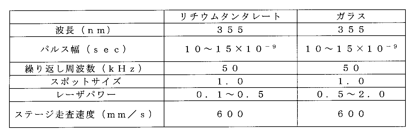
- Tables 1 and 2 show examples of laser irradiation conditions in the case where a thermally denatured layer is formed on a Si substrate, a GaAs substrate, a quartz substrate, a lithium tantalate substrate, and a glass substrate.
- the surface of the single crystal substrate on the laser irradiation side is particularly preferably in a mirror state. In order to make the laser-irradiated surface into a mirror state, for example, mirror polishing can be performed.
- any known single crystal material capable of forming a heat-denatured layer by laser irradiation can be used.
- sapphire, nitride semiconductor, Si, GaAs, quartz crystal, SiC and the like can be mentioned.
- Si, GaAs, quartz, or SiC can be particularly preferably used.
- quartz or glass may be used instead of a single crystal substrate.
- the single crystal substrate a substrate in which at least one surface is mirror-polished is usually used.
- the multilayer film is formed on the mirror-polished surface side.
- a single crystal substrate whose both surfaces are mirror-polished may be used as necessary. In this case, any one surface can be arbitrarily used as a film formation surface.
- the shape of the single crystal substrate in the planar direction is not particularly limited, and may be, for example, a square shape, but may be a circular shape from the viewpoint of easy application in a production line of various known elements.
- a circular shape provided with an orientation flat surface is preferable.
- the diameter of the single crystal substrate is preferably 50 mm or more, more preferably 75 mm or more, and more preferably 150 mm or more. Further preferred.
- the upper limit of the diameter is not particularly limited, but is preferably 300 mm or less from a practical viewpoint.
- the thickness of the single crystal substrate is preferably 5.0 mm or less, preferably 3.0 mm or less, and more preferably 2.0 mm or less.
- the lower limit of the thickness is not particularly limited, and is preferably 0.05 mm or more and more preferably 0.1 mm or more from the viewpoint of ensuring the rigidity of the single crystal substrate.
- the shape of the single crystal substrate 20 is a circular shape or a circular shape provided with an orientation flat surface
- the thickness is preferably 0.3 mm or more, and the diameter is 150 mm.
- the thickness is more than 0.5 mm, the thickness is preferably 0.5 mm or more.
- FIG. 1 is a schematic explanatory view showing an example of a method for manufacturing an internally modified substrate for epitaxial growth according to this embodiment.
- the single crystal substrate 1 fixed to a sample stage (not shown). Fixing is preferably performed so that the warp of the single crystal substrate 1 can be corrected, for example, by vacuum suction or the like. Then, the laser irradiation apparatus 2 irradiates the laser from the surface (film formation surface) side of the single crystal substrate 1 fixed to the sample stage. At this time, the laser is focused inside the thickness direction of the single crystal substrate 1 and the laser irradiation device 2 and the single crystal substrate 1 are relatively moved in the horizontal direction, so that the spot-shaped modified region 3 ( The heat-denatured layer is formed in a continuous line shape.
- the spot-like modified region 3 When viewed locally, the spot-like modified region 3 is formed only in the portion irradiated with the laser instantaneously, and its size depends on the laser spot size, laser intensity, and pulse width.
- the size and degree of modification of the thermally denatured layer with respect to the planar direction and thickness direction of the single crystal substrate 1 can be controlled.
- the length of the spot-shaped modified region 3 formed in a line shape is the relative moving speed of the laser irradiation apparatus 1 with respect to the single crystal substrate 1 (for example, when the sample stage is movable, By appropriately selecting the scanning speed) and the laser repetition frequency, the plurality of heat-denatured layers in the plane direction of the single crystal substrate 1 can be controlled at intervals.
- the modified region 3 is a region formed by locally generating multiphoton absorption in a portion irradiated with a laser.
- the stress of the entire single crystal substrate is controlled, and the warp shape and / or the amount of warpage of the single crystal substrate is precisely controlled. Can be controlled.
- the heat-denatured layer is preferably provided in the pattern shape shown below. That is, the heat-denatured layer is preferably provided in at least one pattern shape selected from the following i) to vii) with respect to the planar direction of the single crystal substrate.
- Concentric circle iv) A shape formed substantially point-symmetrically with respect to the center point of the single crystal substrate v) A shape formed substantially symmetrical with respect to a straight line passing through the center point of the single crystal substrate.
- the shape is preferably i) a shape in which a plurality of polygons having the same shape and the same size are regularly arranged. Further, i) as a shape in which a plurality of polygons having the same shape and the same size are regularly arranged, any one of a plurality of the same shapes and the same size quadrangles adjacent to each other on four sides constituting each quadrangle. It is particularly preferable that the shape is regularly arranged so as to overlap one side, that is, a lattice shape. In this case, laser scanning may be performed only in two directions, ie, the vertical direction and the horizontal direction, and laser processing becomes easier, and design of warpage amount control and shape control of the single crystal substrate becomes easier.
- the pitch of the lines constituting the pattern having the lattice shape is preferably in the range of 50 ⁇ m to 2000 ⁇ m, and more preferably in the range of 100 ⁇ m to 1000 ⁇ m.
- the pitch is preferably in the range of 50 ⁇ m to 2000 ⁇ m, and more preferably in the range of 100 ⁇ m to 1000 ⁇ m.
- FIG. 2 is a plan view showing an example of an arrangement pattern shape of the heat-denatured layer with respect to the planar direction of the single crystal substrate.
- An example of the arrangement pattern shape of a modified layer is shown.
- the arrangement pattern shape of the heat-denaturing layer is, for example, as shown in FIG. 2, for example, a stripe shape in which a plurality of lines are formed perpendicularly or parallel to the orientation flat surface of the substrate (FIGS. 2A and 2B). ), A lattice shape combining both of them (FIG. 2C), and the like.
- regular hexagons of the same size are regularly arranged so that all six vertices of the regular hexagon overlap with any one of the regular hexagons adjacent to the regular hexagon.
- FIG. 2 (d) concentric circular shape
- FIG. 2 (e) concentric circular shape
- the width 4 shown in FIG. 2A means the pitch between lines.
- the warp shape and / or the amount of warpage may be increased depending on the intended use of the internally modified substrate for epitaxial growth. Controlled arbitrarily.
- the stress generated by the film formation can be offset by the stress of the single crystal substrate on which the heat-denatured layer is formed.
- the warping behavior of the substrate can be reduced.
- it is difficult to correct the warp if the heat-denatured layer is provided at a position deviated from the thickness direction or the plane direction of the single crystal substrate, is irregularly arranged, or is asymmetrically arranged. It may become.
- the relative formation position for forming the heat-denatured layer with respect to the thickness direction of the single crystal substrate affects the amount of change in the warp amount of the single crystal substrate after forming the heat-denatured layer, and the amount of change increases as the formation position is closer to the surface. Become.
- the thickness direction of the single crystal substrate is assumed to be a relative position 5 in the thickness direction of the single crystal substrate, and one side serving as the film formation surface is assumed to be 0%.
- the heat-denatured layer is preferably provided in a range of 3% to 95% in the thickness direction of the single crystal substrate, preferably 3% to 50%. More preferably, it is provided within the range.
- the plurality of heat-denatured layers are all present at the same position as the position of the heat-denatured layer in the thickness direction of the single crystal substrate, but they may be present at different positions.
- the individual heat-denatured layers should not be significantly lost so as not to significantly reduce the warping correction effect caused by the provision of the heat-denatured layers. May be arranged at different positions with respect to the thickness direction of the single crystal substrate.
- the length 6 of the thermally denatured layer with respect to the thickness direction of the single crystal substrate is determined depending on the laser spot size, irradiation energy (laser power / repetition frequency), and pulse width, and is usually several ⁇ m to several tens of tens. It is in the range of ⁇ m.
- the warp shape and / or the amount of warpage of the single crystal substrate is controlled efficiently and precisely.
- a modified substrate can be obtained.
- the internal modified substrate with a multilayer film of this embodiment is characterized in that a multilayer film having two or more layers is provided on the film formation surface of the internal modified substrate for epitaxial growth obtained by the present invention. To do.
- the “multilayer film” has two or more layers.
- each layer constituting this multilayer film is composed of continuous layers having the same film thickness in the plane direction of the single crystal substrate, and does not have a step that allows the outermost layer film to penetrate (electrodes). Added to describe that it has no formation site.)
- the layer structure of the multilayer film, and the film thickness, material and crystallinity / non-crystallinity of each layer constituting the multilayer film are prepared by further post-processing using the internal modified substrate with the multilayer film of this embodiment. It is appropriately selected according to the type of element to be manufactured and the manufacturing process applied when manufacturing the element.
- the method for forming the multilayer film is not particularly limited, and a known film formation method can be used, and film formation can be performed by employing different film formation methods and / or film formation conditions for each layer constituting the multilayer film.
- the film forming method include a liquid phase film forming method such as a plating method, but a vapor phase film forming method such as a sputtering method or a CVD method (Chemical Vapor Deposition) is preferably used.
- vapor phase film formation such as MOCVD (Metal Organic Chemical Vapor Deposition), HVPE (Hydride vapor phase epitaxy), MBE (Molecular Beam Epitaxy), etc.
- the method is used. It is particularly preferable that the film formation surface of the internally modified substrate for epitaxial growth is in a mirror state. In order to make the surface on which the multilayer film is formed into a mirror surface state, for example, mirror polishing can be performed.
- At least one of the layers constituting the multilayer film is a crystalline layer.
- at least one of the multilayer films is a nitride semiconductor crystal layer.
- the epitaxial growth can be performed using the crystal plane exposed on the film-forming surface of the epitaxially reformed internal modified substrate, at least the formation of the epitaxially reformed internal modified substrate among the layers constituting the multilayer film.
- the layer in direct contact with the film surface is preferably a crystalline layer, and all layers constituting the multilayer film may be crystalline layers.
- the epitaxial growth includes homoepitaxial growth and heteroepitaxial growth including the same composition or mixed crystal.
- each layer constituting the multilayer film is also appropriately selected according to the element to be manufactured.
- each layer is configured.
- the material is also preferably an inorganic material such as a metal material, a metal oxide material, or an inorganic semiconductor material, and it is desirable that all layers be composed of these inorganic materials.
- MOCVD method when the MOCVD method is used, there is a possibility that a small amount of an organic metal-derived organic substance is mixed in this inorganic material.
- each layer constituting the multilayer film includes various nitride semiconductors such as a light emitting element used for a surface emitting laser, a light receiving element used for an optical sensor or a solar cell, a semiconductor element used for an electronic circuit, etc.
- suitable devices for the manufacture of such devices include GaN-based, AlGaN-based, and InGaN-based nitride semiconductor crystal layers.
- a sapphire substrate is preferably used as the single crystal substrate.
- FIG. 3 is a diagram showing an epitaxial growth process of a nitride semiconductor layer which is an example of a multilayer film.
- a sapphire substrate is used as an internally modified substrate for epitaxial growth, and first, the sapphire substrate is thermally cleaned (FIG. 3A).
- the buffer layer 8 is grown (FIG. 3B).
- an n-GaN layer 9 (FIG. 3C) and an InGaN-based active layer 10 having a multiple quantum well structure are grown (FIG. 3D).
- FIG. 4 shows an in-situ observation example in the epitaxial growth process of the nitride semiconductor layer shown in FIG.
- FIG. 5 is a diagram showing the relationship between the amount of warpage of the substrate and the curvature.
- FIG. 6 is a diagram showing an in-situ observation example when forming the multilayered internal modified substrate according to the present embodiment.
- Non-Patent Document 2 it is possible to quantitatively analyze the behavior of the sapphire substrate during film formation by in-situ observation. That is, it is possible to know how the warpage shape and the warpage amount of the substrate change during film formation.
- the horizontal axis represents time
- the vertical axis represents the curvature (km ⁇ 1 ) of the substrate on the film formation surface.
- the positive direction on the vertical axis indicates that the film formation surface has a convex shape
- the negative direction indicates that the film formation surface has a concave shape.
- the amount of warpage of the substrate can be calculated from the curvature of the substrate.
- the radius of curvature of the substrate is indicated by R
- the amount of warpage X of the substrate having the curvature 1 / R and the diameter of the substrate is approximately indicated by D.
- Spectra A in FIG. 4 shows an example using a conventional sapphire substrate in which a heat-denatured layer is not formed.
- 4A to 4E correspond to the respective steps of the film forming process. That is, it corresponds to (a) substrate thermal cleaning, (b) low temperature buffer layer growth, (c) n-GaN layer growth, (d) InGaN-based active layer growth, and (e) cool down.
- the temperature is lowered to about 700 to 800 ° C., and (d) in the growth stage of the InGaN-based active layer, the thickness of the InGaN-based active layer and the uniformity of the In composition in the InGaN are in the plane of the emission wavelength. Since it affects uniformity, it affects the manufacturing yield of LED chips. Since the film thickness and In composition of the InGaN layer are affected by the film formation temperature, it is ideal that the curvature of the substrate during film formation be as close to 0 as possible in order to improve temperature uniformity within the substrate surface. .
- the substrate curvature in the InGaN-based active layer growth stage can be made almost zero, while the substrate in the film forming process It can be seen that there is a disadvantage that the behavior is large and the curvature of the substrate after film formation is increased.
- a modified region pattern is formed inside a conventional sapphire substrate to produce an epitaxially grown internal modified substrate of the present invention, and a first example of In-situ when a nitride semiconductor layer is formed Is shown in the spectrum B in FIG.
- the modified region pattern is formed so that the film formation surface is warped more convex than the conventional sapphire substrate. Thereby, the warpage behavior of the substrate can be reduced as compared with the spectrum A using the conventional sapphire substrate.
- Spectra C can further reduce the behavior of the substrate throughout the film forming process. That is, the effect of offsetting the stress generated during the film formation with the stress of the substrate is greater than that of the spectra A and B.
- the nitride semiconductor layer obtained in the above-mentioned spectra B and C is less warped of the substrate during film formation and less warped of the substrate than when a conventional sapphire substrate is used. Quality and uniformity are improved.
- the initial state of the internally modified substrate for epitaxial growth greatly warped the convex surface, and as a result, the curvature of the substrate at the InGaN-based active layer growth stage and at the end of film formation was the same as that of the conventional sapphire substrate. The problem of becoming larger than the case occurs.
- the internally modified substrate for epitaxial growth according to the present invention reduces the warping behavior of the substrate as shown by spectrum C in FIG. 6, and at the same time, the growth of the InGaN-based active layer and at the end of film formation. It is desirable that the initial state is such that the curvature can be reduced.
- the quality and uniformity of the nitride semiconductor layer film can be improved, and the uniformity of the emission wavelength of the nitride semiconductor light emitting device can be improved.
- a sapphire substrate that can cancel in advance the substrate curvature that greatly warps the convex surface due to the formation of the heat-denatured layer, before the heat-denatured layer is formed.
- a nitride semiconductor layer having a concave surface and a concave surface with a curvature greater than 0 km ⁇ 1 and 160 km ⁇ 1 can be used as the sapphire substrate for forming the heat-denatured layer.
- the nitride semiconductor layer is formed with a concave surface, and the curvature of the concave surface is preferably 40 km ⁇ 1 or more and 150 km ⁇ 1 or less, more preferably 85 km ⁇ 1 or more and 150 km ⁇ 1 or less.
- an internally modified substrate with a multilayer film provided with a nitride semiconductor layer having improved nitride semiconductor layer quality and uniformity is obtained. be able to.
- Structuring various semiconductor devices using the internal modified substrate with a multilayer film obtained by the present invention can improve device quality and yield.
- the semiconductor device include a light emitting element, an electronic device, a light receiving element, and the like.
- a polishing process, a division line formation process, and a division process may be performed in this order in addition to the element part formation process.
- the device manufacturing method using the internal modified substrate with a multilayer film according to the present embodiment specifically includes the following steps (1) to (4):
- An element including a single crystal substrate having a size substantially corresponding to the element portion can be manufactured.
- the heat-denatured layer remaining in the single crystal substrate is used as a planned dividing line after being polished to such an extent that the heat-denatured layer is not completely removed in the polishing process.
- the multilayer film is individualized into individual element portions, alignment for laser irradiation cannot be performed after confirming the existence positions of the element portions. For this reason, it is difficult to accurately form the planned division lines corresponding to the individual element portions by the above-described method of forming the heat-denatured layer that also functions as the planned division lines before the individual element portions are manufactured. It is.
- a thick film of a crystalline film having a film thickness capable of being self-supporting can be formed by homoepitaxial growth using the internal modified substrate with a multilayer film of the present invention as a base material. Further, the bulk film can be obtained by separating the thick film of the crystalline film from the base material made of the crystal film.
- a bulk substrate made of a thick crystalline film can also be obtained by forming a thick film of a crystalline film on the epitaxially modified internal modified substrate of the present invention and separating it from the epitaxially grown internal modified substrate. Can do.
- the internally modified substrate for epitaxial growth of the present invention warpage of the substrate that occurs during or after film formation can be suppressed, so that a thick film can be formed without generating cracks.
- the above-described nitride semiconductor layer thick film is formed on an epitaxially reformed internal modified substrate, warpage of the substrate that occurs during or after film formation can be suppressed, and self-supporting without generating cracks.
- a thick nitride semiconductor layer having a possible thickness can be obtained.
- the nitride semiconductor bulk substrate can be obtained without using a complicated process by separating the thick film of the nitride semiconductor layer thus obtained from the internal modified substrate.
- the film thickness that can stand by itself is preferably 50 ⁇ m or more.
- an MOCVD method, an HVPE method, an LPE method, or the like can be used as a method for forming a thick film.
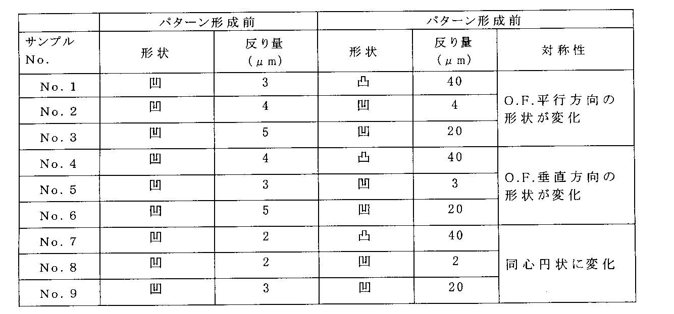
- Example 1 As a sapphire substrate for forming the heat-denatured layer, a 2-inch sapphire substrate with one side polished was used. The substrate thickness was 430 ⁇ m. The warpage shape and warpage amount of the substrate before forming the heat-denatured layer were measured with a laser interferometer.
- a sapphire substrate was placed on the sample stage of the pulse laser device, and a modified region pattern was formed inside the sapphire substrate.
- Table 4 shows the pattern shapes of Samples 1 to 9, the pitch between each line, the formation position, the length of the heat-modified layer, and the processing time per sheet.
- the substrate shape of the sapphire substrate after forming the modified region pattern was measured with a laser interferometer, and the amount of warpage and the substrate thickness were measured with a linear gauge and a laser interferometer.
- ⁇ O. F. Is perpendicular to the orientation flat of the sapphire substrate, // O. F. Indicates that it is parallel to the orientation flat.
- Table 5 shows the warpage shape and warpage amount of the substrate before and after the formation of the modified region pattern, and the symmetry of the warpage shape in the substrate surface after the heat-denatured layer is formed.
- the warpage shape of the substrate indicates the shape on the film formation surface side.
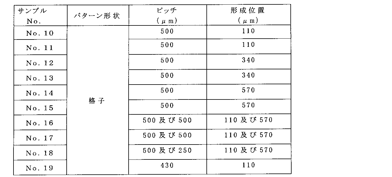
- Example 2 A 4-inch sapphire substrate with one side polished was used as the sapphire substrate for forming the internal modified region pattern.
- the substrate thickness was 650 ⁇ m.
- the warpage shape and the warpage amount of the substrate before forming the modified region pattern were measured with a laser interferometer.
- Table 6 shows the shape, pitch, and formation position of the heat-denatured layers of Samples 10 to 19.
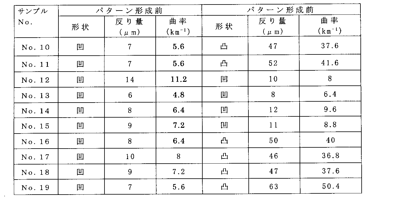
- the warp shape of the substrate after forming the heat-denatured layer was measured with a laser interferometer, and the warp amount was measured with a linear gauge.
- Table 7 shows a comparison of the substrate shape before and after the heat-modified layer formation, the amount of warpage, and the curvature calculated from the amount of warpage.
- the warpage shape of the substrate indicates the shape on the film formation surface side.
- FIG. 7 shows the formation position and the pitch dependence between each line with respect to the change amount of the substrate curvature after the heat-denatured layer is formed.
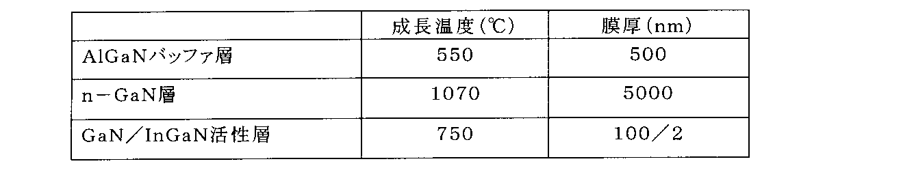
- Example 3 Among the sapphire substrates on which the heat-denatured layer was formed in Example 2, samples 10, 12, 14, 16, and 18 and a conventional sapphire substrate on which no heat-denatured layer was formed (referred to as sample 20) were simultaneously introduced into the MOCVD apparatus. A gallium nitride layer was grown on the sapphire substrate. Table 8 shows the growth temperature and film thickness in each film forming step.
- (1) to (4) in Table 10 are (1) during thermal cleaning transition to the initial state of the substrate, (2) during growth of the n-GaN layer relative to the initial state of the substrate, (3 ) At the time of GaN / InGaN active layer growth transition with respect to the end of n-GaN growth, (4) shows the amount of change in curvature after the end of cool-down with respect to the initial state of the substrate.
- the substrate curvature is smaller than that of the other samples. The effect of suppressing the amount of change was observed.
- Sample 10 was found to have improved film thickness uniformity as compared with sample 20 where the heat-denatured layer was not formed. This is considered to be because the n-GaN layer was grown in a flatter state by forming the heat-denatured layer at a shallow position from the surface of the sapphire substrate.
- the FWHM values of the (001) plane and the (102) plane of the gallium nitride layer obtained by X-ray diffraction rocking curve measurement are 203 arcsec and 418 arcsec for the sample 10, respectively, and for the sample 20 where the heat-denatured layer is not formed, respectively. 242 arcsec and 579 arcsec. From this result, it was found that the crystallinity of the gallium nitride layer was improved in the sample 10 in which the heat-denatured layer was formed compared to the sample 20 in which the heat-denatured layer was not formed.
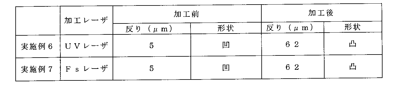
- Example 4 As a sapphire substrate for forming the heat-denatured layer, a 2-inch substrate with one side polished was used. The substrate thickness was 430 ⁇ m. The warpage shape and warpage amount of the substrate before forming the heat-denatured layer were measured with a laser interferometer.
- the above-mentioned two sapphire substrates are respectively placed on the sample stage of the UV laser device having the laser conditions shown in Table 11 and the Fs laser device having the laser conditions shown in Table 3, and the heat-modified layer inside the sapphire substrate. Was formed.
- Table 12 shows the pitch between the lines of Example 4 and Example 5, the formation position, and the laser pulse interval.
- the substrate shape of the sapphire substrate before and after the formation of the thermally denatured layer was measured with a laser interferometer, and the amount of warpage and the substrate thickness were measured with a linear gauge and a laser interferometer.
- Table 13 shows the warpage shape and warpage amount of the substrate before and after the formation of the thermally denatured layer.
- the warpage shape of the substrate indicates the shape on the film formation surface side.
- Example 6 As a sapphire substrate for forming the heat-denatured layer, a 2-inch substrate with one side polished was used. The substrate thickness was 430 ⁇ m. The warpage shape and warpage amount of the substrate before forming the heat-denatured layer were measured with a laser interferometer.
- the above-mentioned two sapphire substrates are respectively placed on the sample stage of the UV laser device having the laser conditions shown in Table 11 and the Fs laser device having the laser conditions shown in Table 3, and the heat-modified layer inside the sapphire substrate. Was formed.
- Table 14 shows the pitch between the lines of Example 6 and Example 7, the formation position, and the laser pulse interval.
- the substrate shape of the sapphire substrate before and after the formation of the thermally denatured layer was measured with a laser interferometer, and the amount of warpage and the substrate thickness were measured with a linear gauge and a laser interferometer.
- Table 15 shows the warpage shape and warpage amount of the substrate before and after the heat-denatured layer was formed.
- the warpage shape of the substrate indicates the shape on the film formation surface side.
- Example 4 using a UV laser with a pulse width of 10 to 15 ns, the width of the processing line to be formed is large because the energy of the laser due to the laser wavelength is large.
- Example 5 under the same processing conditions, in the UV laser processing, the amount of warpage of the substrate alone is further increased, so that the effect of correcting warpage due to the formation of the multilayer film is also greater. For this reason, it has been proved that the processing time can be shortened by using a UV laser when the warping effect of the same substrate alone is obtained. As a result, the manufacturing cost of the internally modified substrate for epitaxial growth can be reduced.
- Example 6 using a UV laser with a pulse width of 10 to 15 ns, the laser irradiation processing line is thick for the same reason as described above. For this reason, compared with Example 7, the processing time which acquires the curvature effect of the same board
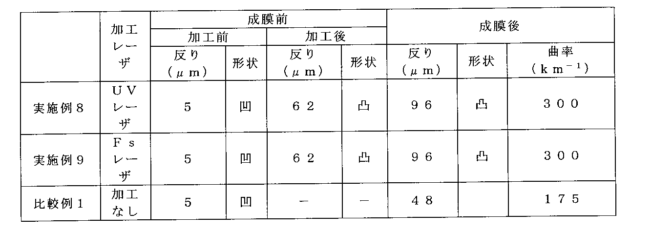
- Example 8 (Examples 8 and 9)
- the sapphire substrate on which the heat-denatured layer was formed and the sapphire substrate on which the heat-denatured layer was not formed were simultaneously introduced into the MOCVD apparatus, and a gallium nitride layer was grown on the substrate.
- the growth temperature and film thickness in each film forming step are the same as the conditions shown in Table 8 above.
- the internally modified substrate for epitaxial growth in which a thermally denatured layer is formed by UV laser irradiation is compared with the internally modified substrate for epitaxial growth in which a thermally denatured layer is formed by Fs laser irradiation.
- the same substrate behavior suppression effect was confirmed during the epitaxial growth of an upward gallium nitride layer. Further, no cracks due to internal cracks caused by intense UV laser irradiation occurred.
Abstract
Description
本発明のエピタキシャル成長用内部改質基板は、単結晶基板と、当該単結晶基板に対するレーザ照射により、その単結晶基板の内部に形成される熱変性層と、を含んでなることを特徴とする。
<照射条件A>
・レーザ波長:200nm~400nm
・パルス幅:ナノ秒オーダー
<照射条件B>
・レーザ波長:400nm~5000nm
・パルス幅:フェムト秒オーダー~ピコ秒オーダー
i)複数個の同一形状および同一サイズの多角形を規則的に配置した形状、
ii)複数個の同一形状および同一サイズの円または楕円を規則的に配置した形状、
iii)同心円状、
iv)単結晶基板の中心点に対して略点対称に形成された形状、
v)単結晶基板の中心点を通じる直線に対して略線対称に形成された形状、
vi)ストライプ形状、ならびに、
vii)らせん形状
から選択される少なくともいずれか1つのパターン形状で設けられていることが好ましい。
(x+y+z=1,x≧0,y≧0,z≧0)からなることが好ましい。
<照射条件A>
・レーザ波長:200nm~400nm
・パルス幅:ナノ秒オーダー
<照射条件B>
・レーザ波長:400nm~5000nm
・パルス幅:フェムト秒オーダー~ピコ秒オーダー
i)複数個の同一形状および同一サイズの多角形を規則的に配置した形状、
ii)複数個の同一形状および同一サイズの円または楕円を規則的に配置した形状、
iii)同心円状、
iv)単結晶基板の中心点に対して略点対称に形成された形状、
v)単結晶基板の中心点を通じる直線に対して略線対称に形成された形状、
vi)ストライプ形状、ならびに、
vii)らせん形状
から選択される少なくともいずれか1つのパターン形状を描くように形成されているが好ましい。
2 レーザ照射装置
3 改質領域
4 ピッチ
5 形成位置
6 熱変性層の長さ
7 サファイア基板
8 低温バッファ層
9 n-GaN層
10 InGaN系活性層
なお、レーザの照射は、熱変性層が形成できるのであれば、如何様な照射条件で実施してもよいが、一般には、短い時間幅の中にエネルギーを集中させることが出来るため、高いピーク出力が得ることができるという点で、断続的にレーザ光を出すパルスレーザを用いて、下記1)および2)に示す範囲内で実施することが好ましい。
1)レーザ波長:200nm~5000nm
2)パルス幅:フェムト秒オーダー~ナノ秒オーダー(1fs~1000ns)
<照射条件A>
・レーザ波長:200nm~400nm
・パルス幅:ナノ秒オーダー(1ns~1000ns)。なお、より好ましくは、10ns~15ns。
<照射条件B>
・レーザ波長:400nm~2000nm
・パルス幅:フェムト秒オーダー~ピコ秒オーダー(1fs~1000ps)。なお、より好ましくは、200fs~800fs。
・パルス幅:50ns~200ns
・繰り返し周波数:10kHz~500kHz
・照射エネルギー:3μJ~30μJ
・レーザのスポットサイズ:0.5μm~4.0μm
・試料ステージの走査速度:50mm/s~1000mm/s(より好ましくは100mm/s~1000mm/s)
・パルス幅:30ns~80ns
・繰り返し周波数:10kHz~500kHz
・照射エネルギー:8μJ~20μJ
・レーザのスポットサイズ:0.5μm~4.0μm
・試料ステージの走査速度:50mm/s~1000mm/s(より好ましくは100mm/s~1000mm/s)
・パルス幅:200fs~800fs
・繰り返し周波数:10kHz~500kHz
・照射エネルギー:3μJ~6μJ
・レーザのスポットサイズ:0.5μm~4.0μm
・試料ステージの走査速度:50mm/s~1000mm/s(より好ましくは100mm/s~1000mm/s)
・パルス幅:200fs~800fs
・繰り返し周波数:10kHz~500kHz
・照射エネルギー:3μJ~6μJ
・レーザのスポットサイズ:0.5μm~4.0μm
・試料ステージの走査速度:50mm/s~1000mm/s(より好ましくは100mm/s~1000mm/s)
・パルス幅:10ns~15ns
・繰り返し周波数:10kHz~500kHz
・照射エネルギー:10μJ~20μJ
・レーザのスポットサイズ:0.5μm~4.0μm
・試料ステージの走査速度:50mm/s~1000mm/s(より好ましくは100mm/s~1000mm/s)

i)複数個の同一形状および同一サイズの多角形を規則的に配置した形状
ii)複数個の同一形状および同一サイズの円または楕円を規則的に配置した形状
iii)同心円状
iv)単結晶基板の中心点に対して略点対称に形成された形状
v)単結晶基板の中心点を通じる直線に対して略線対称に形成された形状
vi)ストライプ形状
vii)らせん形状
(Molecular Beam Epitaxy)等の気相成膜法を利用することがより好ましい。なお、エピタキシャル成長用内部改質基板の成膜面は、鏡面状態であることが特に好ましい。多層膜が形成される面を鏡面状態とするためには、例えば、鏡面研磨を実施することができる。
(1)本実施形態の多層膜付き内部改質基板の多層膜をパターニングして個々の素子部分を形成する素子部分形成工程、
(2)素子部分が片面に形成された素子部分付き単結晶基板の素子部分が形成されていない面を、少なくとも、熱変性層が除去されるまで研磨する研磨工程、
(3)研磨工程において研磨された面側から、個々の素子部分の境界ラインに沿って、レーザを照射することで分割予定ラインを形成する分割予定ライン形成工程、
(4)分割予定ライン形成工程において形成された分割予定ラインに沿って外力を加えることで、素子部分付きの単結晶基板を素子部分単位で分割する分割工程、
ここで、(3)分割予定ライン形成工程、および、(4)分割工程を実施する場合、特許文献3に記載の技術を利用することができる。

熱変性層を形成するサファイア基板として、片面が研磨された2インチサファイア基板を用いた。基板厚みは430μmであった。熱変性層を形成する前の基板の反り形状および反り量はレーザ干渉計で測定した。

内部改質領域パターンを形成するサファイア基板として、片面が研磨された4インチサファイア基板を用いた。基板厚みは650μmであった。実施例1と同様に、改質領域パターン形成前の基板の反り形状および反り量はレーザ干渉計で測定した。
実施例2において熱変性層を形成したサファイア基板のうち、サンプル10,12,14,16,18と、熱変性層未形成の従来のサファイア基板(サンプル20とする)を同時にMOCVD装置に導入し、サファイア基板上への窒化ガリウム層の成長を行った。各成膜工程における成長温度および膜厚を表8に示す。


熱変性層を形成するサファイア基板として、片面が研磨された2インチ基板を用いた。基板厚みは430μmであった。熱変性層を形成する前の基板の反り形状および反り量はレーザ干渉計で測定した。


熱変性層を形成するサファイア基板として、片面が研磨された2インチ基板を用いた。基板厚みは430μmであった。熱変性層を形成する前の基板の反り形状および反り量はレーザ干渉計で測定した。

実施例6,7において熱変性層を形成したサファイア基板と、熱変性層未形成サファイア基板を同時にMOCVD装置に導入し、基板上への窒化ガリウム層の成長を行った。各成膜工程における成長温度および膜厚を上述の表8に示す条件と同じである。
Claims (38)
- 単結晶基板と、
上記単結晶基板に対するレーザ照射により、当該単結晶基板の内部に形成される熱変性層と、
を含んでなることを特徴とするエピタキシャル成長用内部改質基板。 - 請求項1に記載のエピタキシャル成長用内部改質基板において、
前記レーザ照射が、下記AとBに示す少なくともいずれか1つに記載の照射条件を満たすように実施されることを特徴とするエピタキシャル成長用内部改質基板。
<照射条件A>
・レーザ波長:200nm~400nm
・パルス幅:ナノ秒オーダー
<照射条件B>
・レーザ波長:400nm~5000nm
・パルス幅:フェムト秒オーダー~ピコ秒オーダー - 請求項1または請求項2に記載のエピタキシャル成長用内部改質基板において、
前記単結晶基板の厚み方向の相対位置を、成膜面となる片面側を0%と仮定し、上記成膜面と反対側の面を100%とし仮定した際に、
前記熱変性層が、前記単結晶基板の厚み方向の3%以上95%以下の範囲内に設けられていることを特徴とするエピタキシャル成長用内部改質基板。 - 請求項1~3のいずれか1つに記載のエピタキシャル成長用内部改質基板において、
前記熱変性層が、前記単結晶基板の平面方向に対して、
i)複数個の同一形状および同一サイズの多角形を規則的に配置した形状、
ii)複数個の同一形状および同一サイズの円または楕円を規則的に配置した形状、
iii)同心円状、
iv)前記単結晶基板の中心点に対して略点対称に形成された形状、
v)単結晶基板の中心点を通じる直線に対して略線対称に形成された形状、
vi)ストライプ形状、ならびに、
vii)らせん形状
から選択される少なくともいずれか1つのパターン形状で設けられていることを特徴とするエピタキシャル成長用内部改質基板。 - 請求項4に記載のエピタキシャル成長用内部改質基板において、
前記複数個の同一形状および同一サイズの多角形を規則的に配置した形状が、格子形状であることを特徴とするエピタキシャル成長用内部改質基板。 - 請求項5に記載のエピタキシャル成長用内部改質基板において、
前記格子形状を成すパターンを構成するラインのピッチが、50μm以上2000μm以下の範囲内であることを特徴とするエピタキシャル成長用内部改質基板。 - 請求項1~6のいずれか1つに記載のエピタキシャル成長用内部改質基板において、
前記単結晶基板の材質が、サファイア、窒化物半導体、Si、GaAs、水晶およびSiCから選択される少なくともいずれか1種であることを特徴とするエピタキシャル成長用内部改質基板。 - 請求項1~7のいずれか1つに記載のエピタキシャル成長用内部改質基板において、
前記熱変性層を形成する前の前記単結晶基板の形状は、その成膜面が凹面であり、上記凹面の曲率が0km-1より大きく160km-1以下であることを特徴とするエピタキシャル成長用内部改質基板。 - 請求項1~7のいずれか1つに記載のエピタキシャル成長用内部改質基板において、
前記凹面の曲率が40km-1以上150km-1以下であることを特徴とするエピタキシャル成長用内部改質基板。 - 請求項1~7のいずれか1つに記載のエピタキシャル成長用内部改質基板において、
前記凹面の曲率が85km-1以上150km-1以下であることを特徴とするエピタキシャル成長用内部改質基板。 - 請求項1~10のいずれか1つに記載のエピタキシャル成長用内部改質基板において、
前記単結晶基板の直径が50mm以上300mm以下であることを特徴とするエピタキシャル成長用内部改質基板。 - 請求項1~11のいずれか1つに記載のエピタキシャル成長用内部改質基板において、
前記単結晶基板の厚みが0.05mm以上5.0mm以下であることを特徴とするエピタキシャル成長用内部改質基板。 - 請求項1~12のいずれか1つに記載のエピタキシャル成長用内部改質基板において、
前記単結晶基板は、成膜面となる面が研磨面であり、上記単結晶基板に対するレーザ照射が上記研磨面に通じて行われることを特徴とするエピタキシャル成長用内部改質基板。 - 単結晶基板と、
上記単結晶基板に対するレーザ照射により、当該単結晶基板の内部に形成される熱変性層と、を備え、
上記単結晶基板の片面に2つ以上の層を有する多層膜が設けられていることを特徴とする多層膜付き内部改質基板。 - 請求項14に記載の多層膜付き内部改質基板において、
前記多層膜を構成する少なくともいずれか1層が、窒化物半導体結晶層であることを特徴とする多層膜付き内部改質基板。 - 請求項14に記載の多層膜付き内部改質基板を備えることを特徴とする半導体デバイス。
- 請求項16に記載の半導体デバイスは、発光素子、電子デバイス、受光素子のいずれかであることを特徴とする半導体デバイス。
- 請求項14に記載の多層膜付き内部改質基板が備える前記多層膜からなることを特徴とする半導体バルク基板。
- 請求項18に記載の半導体バルク基板において、
AlxInyGazN (x+y+z=1,x≧0,y≧0,z≧0)からなることを特徴とする半導体バルク基板。 - 単結晶基板に対するレーザ照射により、上記単結晶基板の内部に熱変性層を形成することを特徴とするエピタキシャル成長用内部改質基板の製造方法。
- 請求項20に記載のエピタキシャル成長用内部改質基板の製造方法において、
前記レーザ照射が、下記AとBに示す少なくともいずれか1つに記載の照射条件を満たすように実施されることを特徴とするエピタキシャル成長用内部改質基板の製造方法。
<照射条件A>
・レーザ波長:200nm~400nm
・パルス幅:ナノ秒オーダー
<照射条件B>
・レーザ波長:400nm~5000nm
・パルス幅:フェムト秒オーダー~ピコ秒オーダー - 請求項20または請求項21に記載のエピタキシャル成長用内部改質基板の製造方法において、
前記単結晶基板の厚み方向の相対位置を、成膜面となる片面側を0%と仮定し、上記成膜面と反対側の面を100%とし仮定した際に、
前記熱変性層が、前記単結晶基板の厚み方向の3%以上95%以下の範囲内に位置するように形成されることを特徴とするエピタキシャル成長用内部改質基板の製造方法。 - 請求項20~22のいずれか1つに記載のエピタキシャル成長用内部改質基板の製造方法において、
前記熱変性層が、前記単結晶基板の平面方向に対して、
i)複数個の同一形状および同一サイズの多角形を規則的に配置した形状、
ii)複数個の同一形状および同一サイズの円または楕円を規則的に配置した形状、
iii)同心円状、
iv)前記単結晶基板の中心点に対して略点対称に形成された形状、
v)単結晶基板の中心点を通じる直線に対して略線対称に形成された形状、
vi)ストライプ形状、ならびに、
vii)らせん形状
から選択される少なくともいずれか1つのパターン形状を描くように形成されていることを特徴とするエピタキシャル成長用内部改質基板の製造方法。 - 請求項23に記載のエピタキシャル成長用内部改質基板の製造方法において、
前記複数個の同一形状および同一サイズの多角形を規則的に配置した形状が、格子形状であることを特徴とするエピタキシャル成長用内部改質基板の製造方法。 - 請求項24に記載のエピタキシャル成長用内部改質基板において、
前記格子形状を成すパターンを構成するラインのピッチが、50μm以上2000μm以下の範囲内であることを特徴とするエピタキシャル成長用内部改質基板の製造方法。 - 請求項20~25のいずれか1つに記載のエピタキシャル成長用内部改質基板の製造方法において、
前記単結晶基板の材質が、サファイア、窒化物半導体、Si、GaAs、水晶およびSiCから選択される少なくともいずれか1種であることを特徴とするエピタキシャル成長用内部改質基板の製造方法。 - 請求項20~26のいずれか1つに記載のエピタキシャル成長用内部改質基板の製造方法において、
前記熱変性層を形成する前の前記単結晶基板の形状は、その成膜面が凹面であり、上記凹面の曲率が0km-1より大きく160km-1以下であることを特徴とするエピタキシャル成長用内部改質基板の製造方法。 - 請求項20~26のいずれか1つに記載のエピタキシャル成長用内部改質基板の製造方法において、
前記凹面の曲率が40km-1以上150km-1以下であることを特徴とするエピタキシャル成長用内部改質基板の製造方法。 - 請求項20~26のいずれか1つに記載のエピタキシャル成長用内部改質基板の製造方法において、
前記凹面の曲率が85km-1以上150km-1以下であることを特徴とするエピタキシャル成長用内部改質基板の製造方法。 - 請求項20~29のいずれか1つに記載のエピタキシャル成長用内部改質基板の製造方法において、
前記単結晶基板の直径が50mm以上300mm以下であることを特徴とするエピタキシャル成長用内部改質基板の製造方法。 - 請求項20~30のいずれか1つに記載のエピタキシャル成長用内部改質基板の製造方法において、
前記単結晶基板の厚みが0.05mm以上5.0mm以下であることを特徴とするエピタキシャル成長用内部改質基板の製造方法。 - 請求項20~31のいずれか1つに記載のエピタキシャル成長用内部改質基板の製造方法において、
前記単結晶基板は、成膜面となる面が研磨面であり、当該単結晶基板に対する前記レーザ照射が上記研磨面に通じて行われることを特徴とするエピタキシャル成長用内部改質基板の製造方法。 - 単結晶基板に対するレーザ照射により、上記単結晶基板の内部に熱変性層を形成し、
さらに上記単結晶基板の片面に2つ以上の層を有する多層膜が形成することを特徴とする多層膜付き内部改質基板の製造方法。 - 請求項33に記載の多層膜付き内部改質基板の製造方法において、
前記多層膜を構成する少なくともいずれか1層が、窒化物半導体結晶層であることを特徴とする多層膜付き内部改質基板の製造方法。 - 請求項14に記載の多層膜付き内部改質基板を用いて形成することを特徴とする半導体デバイスの製造方法。
- 請求項35に記載の半導体デバイスの製造方法において、
前記半導体デバイスは、発光素子、電子デバイス、受光素子のいずれかであることを特徴とする半導体デバイスの製造方法。 - 請求項14に記載の多層膜付き内部改質基板が備える前記多層膜を用いて形成することを特徴とする半導体バルク基板の製造方法。
- 請求項37に記載の半導体バルク基板の製造方法において、
AlxInyGazN (x+y+z=1,x≧0,y≧0,z≧0)からなることを特徴とする半導体バルク基板の製造方法。
Priority Applications (5)
| Application Number | Priority Date | Filing Date | Title |
|---|---|---|---|
| US13/582,550 US20130161794A1 (en) | 2010-03-05 | 2011-03-04 | Internally reformed substrate for epitaxial growth, internally reformed substrate with multilayer film, semiconductor device, bulk semiconductor substrate, and manufacturing methods therefor |
| EP11750807.7A EP2543752A4 (en) | 2010-03-05 | 2011-03-04 | SUBSTRATE WITH INTERNAL REFORM FOR EPITACTIC GROWTH, INTERNAL REFORMING SUBSTRATE AND A MULTILAYER FILM, SEMICONDUCTOR ELEMENT, MASS SUBSTRATE SUBSTRATE, AND METHOD OF MANUFACTURING THEREOF |
| CN201180009519.0A CN102753737B (zh) | 2010-03-05 | 2011-03-04 | 外延生长用内部改性衬底、带多层膜的内部改性衬底、半导体器件、半导体块状衬底以及它们的制造方法 |
| JP2012503282A JP5802943B2 (ja) | 2010-03-05 | 2011-03-04 | エピタキシャル成長用内部改質基板の製造方法および多層膜付き内部改質基板の製造方法 |
| KR1020127022196A KR101527457B1 (ko) | 2010-03-05 | 2011-03-04 | 에피택셜성장용 내부개질기판, 다층막형성 내부개질기판, 반도체 디바이스, 반도체 벌크 기판 및 그들의 제조 방법 |
Applications Claiming Priority (2)
| Application Number | Priority Date | Filing Date | Title |
|---|---|---|---|
| JP2010049857 | 2010-03-05 | ||
| JP2010-049857 | 2010-03-05 |
Publications (1)
| Publication Number | Publication Date |
|---|---|
| WO2011108698A1 true WO2011108698A1 (ja) | 2011-09-09 |
Family
ID=44542343
Family Applications (1)
| Application Number | Title | Priority Date | Filing Date |
|---|---|---|---|
| PCT/JP2011/055055 WO2011108698A1 (ja) | 2010-03-05 | 2011-03-04 | エピタキシャル成長用内部改質基板、多層膜付き内部改質基板、半導体デバイス、半導体バルク基板およびそれらの製造方法 |
Country Status (7)
| Country | Link |
|---|---|
| US (1) | US20130161794A1 (ja) |
| EP (1) | EP2543752A4 (ja) |
| JP (1) | JP5802943B2 (ja) |
| KR (1) | KR101527457B1 (ja) |
| CN (1) | CN102753737B (ja) |
| TW (1) | TWI508327B (ja) |
| WO (1) | WO2011108698A1 (ja) |
Cited By (5)
| Publication number | Priority date | Publication date | Assignee | Title |
|---|---|---|---|---|
| JP2017121742A (ja) * | 2016-01-07 | 2017-07-13 | 株式会社ディスコ | ウエーハ生成方法 |
| JP2017168675A (ja) * | 2016-03-16 | 2017-09-21 | 富士電機株式会社 | 半導体装置およびその製造方法 |
| KR20190005747A (ko) * | 2017-07-06 | 2019-01-16 | 가부시기가이샤 디스코 | 레이저 가공 장치 및 레이저 가공 방법 |
| WO2020130108A1 (ja) * | 2018-12-21 | 2020-06-25 | 浜松ホトニクス株式会社 | レーザ加工方法、及び、半導体デバイス製造方法 |
| US11201126B2 (en) | 2019-02-05 | 2021-12-14 | Disco Corporation | Method of producing a substrate and system for producing a substrate |
Families Citing this family (14)
| Publication number | Priority date | Publication date | Assignee | Title |
|---|---|---|---|---|
| TWI525664B (zh) * | 2010-03-05 | 2016-03-11 | Namiki Precision Jewel Co Ltd | A crystalline film, a device, and a method for producing a crystalline film or device |
| JP2011201759A (ja) * | 2010-03-05 | 2011-10-13 | Namiki Precision Jewel Co Ltd | 多層膜付き単結晶基板、多層膜付き単結晶基板の製造方法および素子製造方法 |
| KR101491528B1 (ko) * | 2010-03-05 | 2015-02-09 | 나미키 세이미쓰 하우세키 가부시키가이샤 | 단결정 기판, 단결정 기판의 제조 방법, 다층막이 형성된 단결정 기판의 제조 방법 및 소자 제조 방법 |
| TWI499078B (zh) * | 2013-01-31 | 2015-09-01 | Just Innovation Corp | 元件基板、元件基板的製造方法、光電裝置及其製造方法 |
| CN103367117A (zh) * | 2013-07-05 | 2013-10-23 | 江苏能华微电子科技发展有限公司 | 一种基于HVPE工艺的GaN衬底制作方法 |
| JP6119712B2 (ja) * | 2014-10-08 | 2017-04-26 | トヨタ自動車株式会社 | 半導体装置の製造方法 |
| CN104384728B (zh) * | 2014-11-18 | 2016-04-06 | 蓝思科技股份有限公司 | 一种激光加工蓝宝石面板的工艺及夹具 |
| JP5986702B1 (ja) * | 2014-12-03 | 2016-09-06 | 日本碍子株式会社 | 13族元素窒化物層の分離方法および複合基板 |
| CN104630899B (zh) * | 2015-01-17 | 2017-09-22 | 王宏兴 | 金刚石层的分离方法 |
| JP6690983B2 (ja) * | 2016-04-11 | 2020-04-28 | 株式会社ディスコ | ウエーハ生成方法及び実第2のオリエンテーションフラット検出方法 |
| JP6508153B2 (ja) * | 2016-09-21 | 2019-05-08 | 日亜化学工業株式会社 | 発光素子の製造方法 |
| CN111712062B (zh) * | 2020-06-30 | 2021-09-28 | 生益电子股份有限公司 | 一种芯片与pcb的焊接方法 |
| CN111785814B (zh) * | 2020-07-13 | 2021-10-26 | 福建晶安光电有限公司 | 一种衬底及其加工方法、发光二极管及其制造方法 |
| CN112837998B (zh) * | 2021-02-05 | 2023-08-25 | 福建晶安光电有限公司 | 一种衬底加工装置 |
Citations (6)
| Publication number | Priority date | Publication date | Assignee | Title |
|---|---|---|---|---|
| JP3250438B2 (ja) | 1995-03-29 | 2002-01-28 | 日亜化学工業株式会社 | 窒化物半導体発光素子 |
| JP2003264194A (ja) * | 2002-03-11 | 2003-09-19 | Hamamatsu Photonics Kk | レーザゲッタリング方法及び半導体基板 |
| JP2006196558A (ja) * | 2005-01-12 | 2006-07-27 | Namiki Precision Jewel Co Ltd | 窒化物半導体基板の製造方法 |
| JP2006347776A (ja) | 2005-06-13 | 2006-12-28 | Sumitomo Metal Mining Co Ltd | サファイア基板およびその製造方法 |
| JP2008006492A (ja) | 2006-06-30 | 2008-01-17 | Disco Abrasive Syst Ltd | サファイア基板の加工方法 |
| JP2010165817A (ja) * | 2009-01-15 | 2010-07-29 | Namiki Precision Jewel Co Ltd | エピタキシャル成長用内部改質基板及びそれを用いて作製される結晶成膜体、デバイス、バルク基板及びそれらの製造方法 |
Family Cites Families (20)
| Publication number | Priority date | Publication date | Assignee | Title |
|---|---|---|---|---|
| JP3120825B2 (ja) * | 1994-11-14 | 2000-12-25 | 信越半導体株式会社 | エピタキシャルウエーハ及びその製造方法 |
| US6201262B1 (en) * | 1997-10-07 | 2001-03-13 | Cree, Inc. | Group III nitride photonic devices on silicon carbide substrates with conductive buffer interlay structure |
| JP2001253795A (ja) * | 2000-03-09 | 2001-09-18 | Sumitomo Metal Ind Ltd | シリコンエピタキシャルウェーハとその製造方法 |
| JP4120163B2 (ja) * | 2000-12-15 | 2008-07-16 | 株式会社Sumco | Siエピタキシャルウェーハの製造方法及びSiエピタキシャルウェーハ |
| KR100550491B1 (ko) * | 2003-05-06 | 2006-02-09 | 스미토모덴키고교가부시키가이샤 | 질화물 반도체 기판 및 질화물 반도체 기판의 가공 방법 |
| WO2005071720A1 (en) * | 2004-01-26 | 2005-08-04 | Showa Denko K.K. | Group iii nitride semiconductor multilayer structure |
| CN100481337C (zh) * | 2004-12-08 | 2009-04-22 | 雷射先进科技株式会社 | 被分割体的分割起点形成方法、被分割体的分割方法 |
| JP4750720B2 (ja) * | 2004-12-08 | 2011-08-17 | 三星ダイヤモンド工業株式会社 | 被分割体における分割起点形成方法、被分割体の分割方法 |
| JP4189386B2 (ja) * | 2005-01-27 | 2008-12-03 | ローム株式会社 | 窒化物半導体結晶層の成長方法および窒化物半導体発光素子の製法 |
| WO2007055010A1 (ja) * | 2005-11-10 | 2007-05-18 | Renesas Technology Corp. | 半導体装置の製造方法および半導体装置 |
| KR100735532B1 (ko) * | 2006-03-21 | 2007-07-04 | 삼성전자주식회사 | 기판 내에 팽창부를 포함하는 포토마스크 및 포토마스크의표면 평탄화 방법 |
| JP5183892B2 (ja) * | 2006-07-03 | 2013-04-17 | 浜松ホトニクス株式会社 | レーザ加工方法 |
| JP2008108792A (ja) * | 2006-10-23 | 2008-05-08 | Disco Abrasive Syst Ltd | ウエーハの加工方法 |
| JP5130468B2 (ja) * | 2007-07-26 | 2013-01-30 | 株式会社エコトロン | SiCエピタキシャル基板の製造方法 |
| JP5044329B2 (ja) * | 2007-08-31 | 2012-10-10 | 株式会社東芝 | 発光装置 |
| JP5184927B2 (ja) * | 2008-03-21 | 2013-04-17 | パナソニック株式会社 | 窒化物半導体発光素子および窒化物半導体発光素子の製造方法 |
| US8900715B2 (en) * | 2008-06-11 | 2014-12-02 | Infineon Technologies Ag | Semiconductor device |
| JP2011201759A (ja) * | 2010-03-05 | 2011-10-13 | Namiki Precision Jewel Co Ltd | 多層膜付き単結晶基板、多層膜付き単結晶基板の製造方法および素子製造方法 |
| KR101491528B1 (ko) * | 2010-03-05 | 2015-02-09 | 나미키 세이미쓰 하우세키 가부시키가이샤 | 단결정 기판, 단결정 기판의 제조 방법, 다층막이 형성된 단결정 기판의 제조 방법 및 소자 제조 방법 |
| TWI525664B (zh) * | 2010-03-05 | 2016-03-11 | Namiki Precision Jewel Co Ltd | A crystalline film, a device, and a method for producing a crystalline film or device |
-
2011
- 2011-02-14 TW TW100104730A patent/TWI508327B/zh not_active IP Right Cessation
- 2011-03-04 US US13/582,550 patent/US20130161794A1/en not_active Abandoned
- 2011-03-04 EP EP11750807.7A patent/EP2543752A4/en not_active Withdrawn
- 2011-03-04 CN CN201180009519.0A patent/CN102753737B/zh not_active Expired - Fee Related
- 2011-03-04 KR KR1020127022196A patent/KR101527457B1/ko not_active IP Right Cessation
- 2011-03-04 JP JP2012503282A patent/JP5802943B2/ja active Active
- 2011-03-04 WO PCT/JP2011/055055 patent/WO2011108698A1/ja active Application Filing
Patent Citations (6)
| Publication number | Priority date | Publication date | Assignee | Title |
|---|---|---|---|---|
| JP3250438B2 (ja) | 1995-03-29 | 2002-01-28 | 日亜化学工業株式会社 | 窒化物半導体発光素子 |
| JP2003264194A (ja) * | 2002-03-11 | 2003-09-19 | Hamamatsu Photonics Kk | レーザゲッタリング方法及び半導体基板 |
| JP2006196558A (ja) * | 2005-01-12 | 2006-07-27 | Namiki Precision Jewel Co Ltd | 窒化物半導体基板の製造方法 |
| JP2006347776A (ja) | 2005-06-13 | 2006-12-28 | Sumitomo Metal Mining Co Ltd | サファイア基板およびその製造方法 |
| JP2008006492A (ja) | 2006-06-30 | 2008-01-17 | Disco Abrasive Syst Ltd | サファイア基板の加工方法 |
| JP2010165817A (ja) * | 2009-01-15 | 2010-07-29 | Namiki Precision Jewel Co Ltd | エピタキシャル成長用内部改質基板及びそれを用いて作製される結晶成膜体、デバイス、バルク基板及びそれらの製造方法 |
Non-Patent Citations (3)
| Title |
|---|
| J. CRYST. GROWTH, vol. 272, no. 1-4, 2004, pages 94 - 99 |
| JPN. J. APPL. PHYS., vol. 32, 1993, pages 1528 - 1533 |
| See also references of EP2543752A4 |
Cited By (11)
| Publication number | Priority date | Publication date | Assignee | Title |
|---|---|---|---|---|
| JP2017121742A (ja) * | 2016-01-07 | 2017-07-13 | 株式会社ディスコ | ウエーハ生成方法 |
| JP2017168675A (ja) * | 2016-03-16 | 2017-09-21 | 富士電機株式会社 | 半導体装置およびその製造方法 |
| KR20190005747A (ko) * | 2017-07-06 | 2019-01-16 | 가부시기가이샤 디스코 | 레이저 가공 장치 및 레이저 가공 방법 |
| JP2019013953A (ja) * | 2017-07-06 | 2019-01-31 | 株式会社ディスコ | レーザー加工装置およびレーザー加工方法 |
| JP7098284B2 (ja) | 2017-07-06 | 2022-07-11 | 株式会社ディスコ | レーザー加工装置およびレーザー加工方法 |
| KR102537095B1 (ko) | 2017-07-06 | 2023-05-25 | 가부시기가이샤 디스코 | 레이저 가공 장치 및 레이저 가공 방법 |
| WO2020130108A1 (ja) * | 2018-12-21 | 2020-06-25 | 浜松ホトニクス株式会社 | レーザ加工方法、及び、半導体デバイス製造方法 |
| JP2020102521A (ja) * | 2018-12-21 | 2020-07-02 | 浜松ホトニクス株式会社 | レーザ加工方法、及び、半導体デバイス製造方法 |
| JP7330695B2 (ja) | 2018-12-21 | 2023-08-22 | 浜松ホトニクス株式会社 | レーザ加工方法、及び、半導体デバイス製造方法 |
| US11201126B2 (en) | 2019-02-05 | 2021-12-14 | Disco Corporation | Method of producing a substrate and system for producing a substrate |
| TWI783208B (zh) * | 2019-02-05 | 2022-11-11 | 日商迪思科股份有限公司 | 生產襯底的方法以及生產襯底的系統 |
Also Published As
| Publication number | Publication date |
|---|---|
| KR101527457B1 (ko) | 2015-06-10 |
| TW201201407A (en) | 2012-01-01 |
| TWI508327B (zh) | 2015-11-11 |
| KR20120123472A (ko) | 2012-11-08 |
| CN102753737A (zh) | 2012-10-24 |
| CN102753737B (zh) | 2015-12-16 |
| EP2543752A4 (en) | 2015-12-02 |
| US20130161794A1 (en) | 2013-06-27 |
| JPWO2011108698A1 (ja) | 2013-06-27 |
| JP5802943B2 (ja) | 2015-11-04 |
| EP2543752A1 (en) | 2013-01-09 |
Similar Documents
| Publication | Publication Date | Title |
|---|---|---|
| JP5802943B2 (ja) | エピタキシャル成長用内部改質基板の製造方法および多層膜付き内部改質基板の製造方法 | |
| JP5552627B2 (ja) | エピタキシャル成長用内部改質基板及びそれを用いて作製される結晶成膜体、デバイス、バルク基板及びそれらの製造方法 | |
| JP5732684B2 (ja) | 単結晶基板、単結晶基板の製造方法、多層膜付き単結晶基板の製造方法および素子製造方法 | |
| TWI550690B (zh) | A single crystal substrate having a multilayer film, a manufacturing method of a single crystal substrate having a multilayer film, and an element manufacturing method | |
| TWI525664B (zh) | A crystalline film, a device, and a method for producing a crystalline film or device | |
| JP6424345B2 (ja) | GaN基板の製造方法 | |
| US20160265140A1 (en) | Single crystal substrate, manufacturing method for single crystal substrate, manufacturing method for single crystal substrate with multilayer film, and element manufacturing method | |
| JP2008308384A (ja) | Iii族窒化物結晶基板の製造方法、iii族窒化物結晶基板、および半導体デバイス |
Legal Events
| Date | Code | Title | Description |
|---|---|---|---|
| WWE | Wipo information: entry into national phase |
Ref document number: 201180009519.0 Country of ref document: CN |
|
| 121 | Ep: the epo has been informed by wipo that ep was designated in this application |
Ref document number: 11750807 Country of ref document: EP Kind code of ref document: A1 |
|
| WWE | Wipo information: entry into national phase |
Ref document number: 1933/MUMNP/2012 Country of ref document: IN |
|
| WWE | Wipo information: entry into national phase |
Ref document number: 2012503282 Country of ref document: JP |
|
| ENP | Entry into the national phase |
Ref document number: 20127022196 Country of ref document: KR Kind code of ref document: A |
|
| NENP | Non-entry into the national phase |
Ref country code: DE |
|
| WWE | Wipo information: entry into national phase |
Ref document number: 2011750807 Country of ref document: EP |
|
| WWE | Wipo information: entry into national phase |
Ref document number: 13582550 Country of ref document: US |