WO2011104967A1 - 電子デバイス - Google Patents
電子デバイス Download PDFInfo
- Publication number
- WO2011104967A1 WO2011104967A1 PCT/JP2010/071442 JP2010071442W WO2011104967A1 WO 2011104967 A1 WO2011104967 A1 WO 2011104967A1 JP 2010071442 W JP2010071442 W JP 2010071442W WO 2011104967 A1 WO2011104967 A1 WO 2011104967A1
- Authority
- WO
- WIPO (PCT)
- Prior art keywords
- ceramic
- heat
- heat conducting
- light emitting
- glass
- Prior art date
- Legal status (The legal status is an assumption and is not a legal conclusion. Google has not performed a legal analysis and makes no representation as to the accuracy of the status listed.)
- Ceased
Links
Images




Classifications
-
- H—ELECTRICITY
- H10—SEMICONDUCTOR DEVICES; ELECTRIC SOLID-STATE DEVICES NOT OTHERWISE PROVIDED FOR
- H10W—GENERIC PACKAGES, INTERCONNECTIONS, CONNECTORS OR OTHER CONSTRUCTIONAL DETAILS OF DEVICES COVERED BY CLASS H10
- H10W40/00—Arrangements for thermal protection or thermal control
- H10W40/20—Arrangements for cooling
- H10W40/22—Arrangements for cooling characterised by their shape, e.g. having conical or cylindrical projections
- H10W40/226—Arrangements for cooling characterised by their shape, e.g. having conical or cylindrical projections characterised by projecting parts, e.g. fins to increase surface area
- H10W40/228—Arrangements for cooling characterised by their shape, e.g. having conical or cylindrical projections characterised by projecting parts, e.g. fins to increase surface area the projecting parts being wire-shaped or pin-shaped
-
- H—ELECTRICITY
- H10—SEMICONDUCTOR DEVICES; ELECTRIC SOLID-STATE DEVICES NOT OTHERWISE PROVIDED FOR
- H10H—INORGANIC LIGHT-EMITTING SEMICONDUCTOR DEVICES HAVING POTENTIAL BARRIERS
- H10H20/00—Individual inorganic light-emitting semiconductor devices having potential barriers, e.g. light-emitting diodes [LED]
- H10H20/80—Constructional details
- H10H20/85—Packages
- H10H20/858—Means for heat extraction or cooling
- H10H20/8581—Means for heat extraction or cooling characterised by their material
-
- H—ELECTRICITY
- H10—SEMICONDUCTOR DEVICES; ELECTRIC SOLID-STATE DEVICES NOT OTHERWISE PROVIDED FOR
- H10H—INORGANIC LIGHT-EMITTING SEMICONDUCTOR DEVICES HAVING POTENTIAL BARRIERS
- H10H20/00—Individual inorganic light-emitting semiconductor devices having potential barriers, e.g. light-emitting diodes [LED]
- H10H20/80—Constructional details
- H10H20/85—Packages
- H10H20/858—Means for heat extraction or cooling
- H10H20/8582—Means for heat extraction or cooling characterised by their shape
Definitions
- the present invention relates to an electronic device including an electronic element such as a light emitting element or an integrated circuit.
- the conventional light emitting device includes a light emitting element (101) such as an LED (Light Emitting Diode) and a package (100) for mounting the light emitting element (101) (for example, , See Patent Document 1).
- the package (100) includes a ceramic base (102) and a ceramic frame (103), and the frame (103) is joined and integrated with the upper surface (102a) of the base (102).
- a cavity (103a) for accommodating the light emitting element (101) is formed.
- the light emitting element (101) is accommodated in the cavity (103a) of the package (100), and is installed in a region of the upper surface (102a) of the base body (102) to be the bottom surface of the cavity (103a).
- the base (102) is provided with a heat conduction part (104) for guiding the heat generated from the light emitting element (101) to the lower surface (102b) of the base (102).
- the heat conduction part (104) is provided in the base body (102), and the via (105) penetrating from the upper surface (102a) to the lower surface (102b) of the base body (102), and filling the via (105) And a heat conductive material (106) formed.
- the heat conductive material (106) is exposed on the upper surface (102a) of the base body (102) to form an exposed surface (104a) of the heat conductive portion (104), and the light emitting element is formed on the exposed surface (104a). (101) is installed.
- the entire exposed surface (104a) of the heat conducting portion (104) is covered with the light emitting element (101) or the exposed surface (not shown) (not shown).
- a part of the peripheral region of 104a) was covered with the light emitting element (101). Therefore, as shown in FIG. 12, the lower surface of the light emitting element (101) is in contact with only the raised portion, and the contact area between the light emitting element (101) and the exposed surface (104a) of the heat conducting portion (104) is reduced. There was a fear.
- an object of the present invention is to provide an electronic device having high heat dissipation characteristics and high reliability.
- the electronic device includes a ceramic base, an electronic element mounted on the surface of the base, and a heat conduction portion that guides heat generated from the electronic element to the back surface of the base.
- the heat conducting portion is formed of a via that is opened in the base and penetrates from the surface to the back of the base, and a heat conductive material that is filled in the via, and the heat conductive material is exposed on the surface of the base. An exposed surface of the heat conducting portion is formed, and the electronic element is disposed on the exposed surface.
- the installation area of the electronic element is surrounded by a peripheral area of the exposed surface of the heat conducting part, and the heat conduction Of the exposed surface of the part, a region different from the region where the electronic element is installed is covered with a ceramic layer.
- the peripheral area of the exposed surface of the heat conducting portion may be raised, and a raised portion may be formed on the exposed surface.
- the region inside the peripheral region (the region surrounded by the peripheral region) of the exposed surface of the heat conducting unit tends to remain flat even when the peripheral region is raised.
- the peripheral region of the exposed surface of the heat conducting part is not covered with the electronic element, and therefore the raised part of the heat conducting part and the electronic element do not overlap. That is, the electronic element is installed in a flat region on the exposed surface of the heat conducting unit. Therefore, the contact area between the lower surface of the electronic element and the exposed surface of the heat conducting unit is large, and therefore the heat generated from the electronic element easily moves to the heat conducting unit. As a result, the amount of heat dissipated from the back surface of the substrate increases, and the electronic device has high heat dissipation characteristics.
- the electronic device In the electronic device, a region different from the region where the electronic element is installed is covered with a ceramic layer in the exposed surface of the heat conducting portion. Therefore, it is difficult for a chemical reaction such as oxidation to occur on the exposed surface of the heat conducting portion, and thus the heat conducting portion is prevented from being deteriorated, and as a result, the reliability of the electronic device is improved.
- the electronic device further includes a ceramic frame body that is bonded to the surface of the base body and forms a cavity for accommodating the electronic element, and exposing the heat conducting unit.
- the surface extends to a position below the frame, and the peripheral area of the exposed surface is covered with the frame.
- the electronic element is a light emitting element
- the ceramic layer contains glass, and a part of the glass is deposited on the surface of the ceramic layer.
- a glass layer is formed on the surface of the ceramic layer, and a light reflecting surface is formed by the surface of the glass layer. Therefore, light emitted obliquely downward from the light emitting element is reflected on the surface of the glass layer and travels upward, and as a result, high emission intensity is obtained in the electronic device.
- the crystallinity of the glass deposited on the surface of the ceramic layer is greater than 3%.
- a glass layer having a glass crystallinity greater than 3% has a smaller surface roughness than a glass layer having a glass crystallinity of 3% or less. Accordingly, a glass layer having a glass crystallinity greater than 3% has a light reflecting surface with a high light reflectance. Therefore, higher emission intensity can be obtained in the electronic device.
- the base is formed of a low-temperature co-fired ceramic that can be co-fired with a heat conductive material constituting the heat conductive portion.
- the electronic device according to the present invention has high heat dissipation characteristics and high reliability.
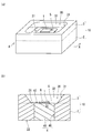
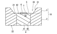
- FIG. 1A is a perspective view showing a light emitting device according to an embodiment of the present invention
- FIG. 1B is a cross-sectional view taken along the line AA shown in FIG.
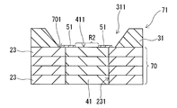
- FIG. 2 is a cross-sectional view used for explaining a ceramic body forming step of the method for manufacturing a light emitting device.
- FIG. 3 is a cross-sectional view showing a package manufactured by executing the firing step of the manufacturing method.
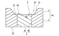
- FIG. 4 is a cross-sectional view used for explaining the plating process of the manufacturing method.
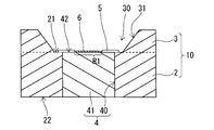
- FIG. 5 is a cross-sectional view used for explaining an element mounting process of the manufacturing method.
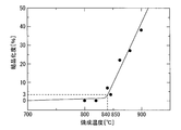
- FIG. 6 is a diagram showing the relationship between the firing temperature and the crystallinity of the glass.
- FIG. 7 is a diagram showing the relationship between the wavelength of light incident on the surface of the ceramic layer and the reflectance of the light.
- FIG. 8 is a cross-sectional view showing a first modification of the light emitting device.
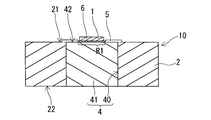
- FIG. 9 is a cross-sectional view showing a second modification of the light emitting device.
- FIG. 10 is a cross-sectional view showing a third modification of the light emitting device.
- FIG. 11 is a cross-sectional view showing a conventional light emitting device.
- FIG. 12 is an enlarged view of the exposed surface of the heat conducting portion of the conventional light emitting device.
- FIG. 1 (a) is a perspective view showing a light emitting device according to an embodiment of the present invention
- FIG. 1 (b) is a cross-sectional view taken along line AA shown in FIG. 1 (a).
- the light emitting device of this embodiment includes an LED (1) and a package (10) for mounting the LED (1).
- the package (10) is composed of a ceramic base (2) and a ceramic frame (3), and the frame (3) is joined and integrated with the upper surface (21) of the base (2). .
- a cavity (30) for accommodating the LED (1) is formed from the inner peripheral surface (31) of the frame (3) and the upper surface (21) of the base body (2).
- the LED (1) is accommodated in the cavity (30) of the package (10), and is installed on a region of the upper surface (21) of the base body (2) that becomes the bottom surface of the cavity (30).
- the cavity (30) is filled with a resin material (32) containing a phosphor.
- the base body (2) is provided with a heat conduction part (4) for guiding the heat generated from the LED (1) to the lower surface (22) of the base body (2).
- the heat conduction part (4) is opened in the base body (2) and is filled in the via (40) penetrating from the upper surface (21) to the lower surface (22) of the base body (2).
- a heat conductive material (41) is exposed on the upper surface (21) of the base body (2) to form an exposed surface (42) of the heat conducting portion (4).
- the LED ( 1) is installed on the exposed surface (42).
- a metal material having high heat conductivity such as silver (Ag) or an alloy of silver (Ag) and platinum (Pt) is used.
- the ceramic material constituting the base body (2) and the frame (3) can be co-fired with the heat conduction material (41) constituting the heat conduction section (4) at a low temperature co-firing.
- Ceramic (LTCC) is used.
- LTCC low-temperature co-fired ceramic
- alumina and glass at a predetermined ratio is used.
- the exposed surface (42) of the heat conducting part (4) extends to the outside of the installation area R1 of the LED (1), and thereby the installation area of the LED (1).
- R1 is surrounded by the peripheral region of the exposed surface (42) of the heat conducting part (4).
- region R1 of LED (1) is coat
- the ceramic layer (5) contains glass, and a part of the glass is deposited on the surface of the ceramic layer (5). And in the light emitting device of this embodiment, the glass deposited on the surface of the ceramic layer (5) has a crystallinity greater than 3%.
- a gold plating layer (6) is formed in the installation region R1 of the LED (1) in the exposed surface (42) of the heat conduction part (4), and the LED (1) is formed on the surface of the gold plating layer (6). ) Is installed.
- this manufacturing method has a ceramic body formation process, a baking process, a plating process, an element mounting process, and a resin filling process, and these processes are executed in this order.
- FIG. 2 is a cross-sectional view used for explaining the ceramic body forming process.
- a plurality of ceramic sheets (23) made from low-temperature co-fired ceramic (LTCC) are laminated to form a laminated body (70).
- LTCC low-temperature co-fired ceramic
- a through hole (231) penetrating from the front surface to the back surface is formed in a predetermined region, and the through hole (231) is filled with a heat conductive material (41). .
- LTCC low-temperature co-fired ceramic
- a metal material having high thermal conductivity such as silver (Ag) or an alloy of silver (Ag) and platinum (Pt) is used for the heat conductive material (41).
- a frame forming body (31) which is made of a low-temperature co-fired ceramic (LTCC) and becomes a frame body (3) after firing is placed on the upper surface (701) of the laminated body (70).
- the frame forming body (31) is placed on the upper surface (701) of the multilayer body (70) with the uppermost surface (411) of the heat conductive material (41) exposed in the space (311) inside thereof.
- the frame forming body (31) may be formed by pressing and sintering the low-temperature co-fired ceramic powder into a predetermined shape, or may be formed by laminating a plurality of ceramic sheets in the same manner as the laminated body (70). Good.
- a formation layer (51) to be a ceramic layer (5) is further formed on the upper surface (701) of the multilayer body (70). Specifically, among the uppermost surface (411) of the heat conductive material (41) exposed on the upper surface (701) of the laminated body (70), the region R2 to be the installation region R1 of the LED (1) is left, and the others. These regions are covered with a forming layer (51).
- the formation layer (51) may be formed by covering the other region with a ceramic sheet, or may be formed by applying a ceramic paint on the other region.
- a ceramic body (71) composed of the laminate (70), the formation layer (51), and the frame formation body (31) is formed.
- the ceramic body (71) produced in the ceramic body forming step is fired at a temperature of 840 ° C. or higher and lower than 950 ° C.
- a low-temperature co-fired ceramic (LTCC) is used for the ceramic body (71). Therefore, the ceramic body (71) can be sintered even when the firing temperature is a low temperature of 840 ° C. or higher and lower than 950 ° C. If the firing temperature is 840 ° C. or higher and lower than 950 ° C., the metal material such as silver (Ag) used as the heat conductive material (41) is sintered without causing abnormal shrinkage.
- FIG. 3 is a cross-sectional view showing a package manufactured by executing the firing process.
- the laminate (70) and the frame forming body (31) are sintered to form the base (2) and the frame (3), and the base (2 ) And the frame (3) are joined together.
- a cavity (30) for housing the LED (1) is formed from the inner peripheral surface (31) of the frame (3) and the upper surface (21) of the base body (2).
- the through holes (231) formed in the plurality of ceramic sheets (23) are connected to each other, and the base (2) penetrates from the upper surface (21) to the lower surface (22).
- a via (40) is formed.
- the heat conductive material (41) filled in the through hole (231) is also sintered, and the heat conductive materials (41) are combined and integrated with each other. The Thereby, the heat conduction part (4) is formed, and the uppermost surface (411) of the heat conduction material (41) before firing becomes the exposed surface (42) of the heat conduction part (4) after firing.
- the formation layer (51) is sintered and the ceramic layer (5) is formed by executing the firing step.
- the region R2 that was left uncovered by the formation layer (51) before firing is the region where the LED (1) is placed after firing. R1.
- a package (10) for mounting the LED (1) is formed.
- FIG. 4 is a cross-sectional view used for explaining the plating process.
- the gold plating layer (6) is formed in the installation region R1 by performing gold plating on the installation region R1 of the LED (1) in the upper surface (21) of the base body (2). To do.
- FIG. 5 is a cross-sectional view used for explaining the element mounting process.
- the LED (1) is mounted on the package (10). Specifically, the LED (1) is accommodated in the cavity (30) of the package (10). At this time, LED (1) is installed on the surface of the gold plating layer (6).
- the cavity (30) of the package (10) is filled with a resin material (32) containing a phosphor.
- a resin material (32) containing a phosphor As shown in FIGS. 1A and 1B, the light emitting device according to the present embodiment is completed.
- the peripheral region of the exposed surface (42) of the heat conducting portion (4) is raised and a raised portion is formed on the exposed surface (42) (see FIG. 12).
- the region inside the peripheral region (the region surrounded by the peripheral region) among the exposed surface (42) of the heat conducting part (4) tends to remain flat even when the peripheral region is raised.
- the peripheral region of the exposed surface (42) of the heat conducting part (4) is not covered with the LED (1), and therefore the raised part of the heat conducting part (4) and the LED (1) Do not overlap. That is, LED (1) is installed in the flat area
- the gold plating layer (6) is the heat conduction part ( 4) is formed along the unevenness of the exposed surface (42).), And the heat generated from the LED (1) easily moves to the heat conduction section (4). As a result, the amount of heat dissipated from the lower surface (22) of the substrate (2) is increased, and the light emitting device has high heat dissipation characteristics.
- the exposed surface (42) of the heat conduction part (4) is expanded to the outside of the installation region R1, and the heat conduction part (4) is thickened as shown in FIG.
- the amount of heat transferred from the upper surface (21) to the lower surface (22) of the substrate (2) in 4) increases, and as a result, the light emitting device has higher heat dissipation characteristics.
- the light emitting device a region different from the installation region R1 of the LED (1) in the exposed surface (42) of the heat conducting unit (4) is covered with the ceramic layer (5).
- the installation region R1 of the LED (1) is covered with a gold plating layer (6).
- the resin material (32) does not come into contact with the exposed surface (42) of the heat conducting section (4). Therefore, the exposed surface (42) of the heat conduction part (4) hardly undergoes a chemical reaction (oxidation or the like) with the phosphor contained in the resin material (32), and therefore the heat conduction part (4) is deteriorated. As a result, the reliability of the light emitting device is improved.
- glass is contained in the ceramic layer (5), and a part of the glass is deposited on the surface of the ceramic layer (5). Therefore, a glass layer is formed on the surface of the ceramic layer (5) by the deposited glass, and a light reflecting surface is formed by the surface of the glass layer. Therefore, the light emitted diagonally downward from the LED (1) is reflected on the surface of the glass layer and travels upward, and as a result, high light emission intensity is obtained in the light emitting device. .
- the crystallinity of the glass deposited from the ceramic layer (5) is greater than 3%.
- a glass layer having a glass crystallinity greater than 3% has a smaller surface roughness than a glass layer having a glass crystallinity of 3% or less. Accordingly, a glass layer having a glass crystallinity greater than 3% has a light reflecting surface with a high light reflectance. Therefore, higher light emission intensity can be obtained in the light emitting device.
- the inventor of the present application confirmed by experiments that the light reflectance at the surface of the glass layer formed by the precipitated glass is high when the crystallinity of the glass deposited from the ceramic layer (5) is greater than 3%. It was.
- FIG. 6 is a graph showing the relationship between the firing temperature of the ceramic body (71) and the crystallinity of the precipitated glass.
- the crystallinity of the glass was measured using an X-ray diffraction method. Specifically, with respect to a package produced by firing the ceramic body (71), the peak value I (Al 2 O of the X-ray diffraction intensity of alumina and glass of low temperature co-fired ceramic (LTCC) constituting the package. 3 ) and I (glass) were measured, respectively, and the ratio of the glass peak value I (glass) to the alumina peak value I (Al 2 O 3 ) was determined to obtain the crystallinity.
- LTCC low temperature co-fired ceramic
- the firing temperature is 840 ° C. or higher, the crystallinity of the precipitated glass is greater than 3%.
- the firing temperature is about 900 ° C.
- the crystallinity of the precipitated glass is about 40%
- the firing temperature is about 950 ° C. (not shown)
- the crystallinity of the precipitated glass is 60%. It will be about.
- the firing temperature is less than 840 ° C., the crystallinity of the precipitated glass is 3% or less.
- FIG. 7 shows the wavelength of light incident on the surface of the ceramic layer (5) and the reflectance of the light for each of the packages (10) manufactured at firing temperatures of 847 ° C., 900 ° C., and 950 ° C.
- FIG. 6 is a diagram showing the relationship by graphs A1 to A3. From the graph shown in FIG. 7, it can be seen that a high light reflectance of 85% or more can be obtained in the package (10) manufactured at a baking temperature of 847 ° C. In addition, it can be seen that in the package (10) manufactured at a firing temperature higher than 847 ° C. (900 ° C. and 950 ° C.), the light reflectance is further increased particularly in the wavelength regions of 380 nm to 450 nm and 600 nm to 780 nm.
- Tables 1 and 2 respectively represent the light reflectance when the wavelength of the incident light is 405 nm and 650 nm with respect to the graph shown in FIG. As shown in Table 1, when the wavelength of incident light is 405 nm, the light reflectance is 97% at a firing temperature of 847 ° C. and 101.2% at a firing temperature of 900 ° C. Further, as shown in Table 2, when the wavelength of incident light is 650 nm, the light reflectance is 89.8% at a firing temperature of 847 ° C. and 91.8% at a firing temperature of 900 ° C.
- FIG. 8 is a cross-sectional view showing a first modification of the light emitting device.
- the exposed surface (42) of the heat conducting part (4) extends to a position below the frame (3), and the peripheral region of the exposed surface (42) is the frame ( It may be covered by 3).
- the light emitting device According to the light emitting device according to the first modified example, it is possible to prevent the protruding portion from appearing on the bottom surface of the cavity (30), and thus the high smoothness of the bottom surface of the cavity (30) is maintained.
- FIG. 9 is a cross-sectional view showing a second modification of the light emitting device. As shown in FIG. 9, the light emitting device may have a configuration without the frame (3).
- FIG. 10 is a cross-sectional view showing a third modification of the light emitting device.
- the heat conducting portions (4) are provided at a plurality of locations of the base body (2), and the central portion of each heat conducting portion (4) is made thin, while each heat conducting portion (4
- the upper and lower portions of the heat conducting portions (4) to (4) may be connected to each other by expanding the upper and lower portions.
- each heat conduction part (4) has a shape where the center part was thin and the upper part and the lower part were expanded. Therefore, in the ceramic body forming step, it becomes easy to fill the vias (40) constituting the heat conducting portions (4) with the heat conducting material (41).
- each part of the present invention is not limited to the above-described embodiment, and various modifications can be made within the technical scope described in the claims.
- the ceramic material, the heat conductive material (41), and the like employed in the light emitting device are not limited to the materials described in the above embodiment, and various materials can be used.
- the various configurations adopted for the light emitting device can also be applied to light emitting devices having light emitting elements other than LEDs.
- the various configurations employed in the light emitting device can be applied not only to light emitting devices including light emitting elements but also to electronic devices including various electronic elements that generate heat, such as integrated circuits.
- LED electronic element
- Substrate (21) Top surface (surface) (22) Bottom (rear) (3) Frame (30) Cavity (32) Resin material (4) Heat conduction part (40) Via (41) Heat conduction material (42) Exposed surface (5) Ceramic layer (6) Gold plating layer R1 installation area
Landscapes
- Led Device Packages (AREA)
- Cooling Or The Like Of Semiconductors Or Solid State Devices (AREA)
Abstract
本発明に係る電子デバイスは、セラミック製の基体2と、該基体2の表面に搭載された電子素子1と、該電子素子1から発生した熱を基体2の背面へ導く熱伝導部4とを具えている。該熱伝導部4は、基体2に開設されて該基体2の表面から背面へ貫通するビア40と、該ビア40に充填された熱伝導材41とから構成され、該熱伝導材41が基体2の表面に露出して熱伝導部4の露出面42が形成されており、該露出面42上に電子素子1が設置されている。ここで、熱伝導部4の露出面42が電子素子1の設置領域R1の外側まで拡がることにより、該電子素子1の設置領域R1が、熱伝導部4の露出面42の周縁領域によって包囲されており、熱伝導部4の露出面42の内、電子素子1の設置領域R1とは異なる領域がセラミック層5により被覆されている。
Description
本発明は、発光素子や集積回路などの電子素子を具えた電子デバイスに関する。
従来の発光デバイスは、図11に示す様に、LED(Light Emitting Diode)等の発光素子(101)と、該発光素子(101)を搭載するためのパッケージ(100)とを具えている(例えば、特許文献1参照)。該パッケージ(100)は、セラミック製の基体(102)と、セラミック製の枠体(103)とから構成され、枠体(103)が基体(102)の上面(102a)に接合一体化されることにより、発光素子(101)を収容するためのキャビティ(103a)が形成されている。発光素子(101)は、パッケージ(100)のキャビティ(103a)に収容されて、基体(102)の上面(102a)の内、キャビティ(103a)の底面となる領域に設置されている。
又、基体(102)には、発光素子(101)から発生した熱を基体(102)の下面(102b)へ導く熱伝導部(104)が設けられている。ここで、熱伝導部(104)は、基体(102)に開設されて該基体(102)の上面(102a)から下面(102b)へ貫通するビア(105)と、該ビア(105)に充填された熱伝導材(106)とから構成されている。そして、熱伝導材(106)が基体(102)の上面(102a)に露出して熱伝導部(104)の露出面(104a)が形成されており、該露出面(104a)上に発光素子(101)が設置されている。
上記発光デバイスにおいて、基体(102)を構成しているセラミック材と熱伝導材(106)との間には、熱膨張率の差が存在している。従って、上記発光デバイスの製造過程において、図12に示す様に、熱伝導部(104)の露出面(104a)の周縁領域が隆起して、該露出面(104a)に隆起部が形成される虞がある。
ところが、従来の発光デバイスにおいては、図11に示す様に熱伝導部(104)の露出面(104a)の全域が発光素子(101)により覆われ、或いは、図示していないが該露出面(104a)の周縁領域の一部が発光素子(101)により覆われていた。このため、発光素子(101)の下面が、図12に示す様に隆起部とのみ接触し、発光素子(101)と熱伝導部(104)の露出面(104a)との接触面積が小さくなる虞があった。該接触面積が小さいと、発光素子(101)から熱伝導部(104)へ熱が移動し難く、従って、発光素子(101)から発生した熱は基体(102)の下面(102b)へ移動し難くなる。よって、基体(102)の下面(102b)から発散される熱量が小さくなって、発光デバイスの放熱特性が低下することになる。
そこで本発明の目的は、高い放熱特性と高い信頼性とを有する電子デバイスを提供することである。
本発明に係る電子デバイスは、セラミック製の基体と、該基体の表面に搭載された電子素子と、該電子素子から発生した熱を基体の背面へ導く熱伝導部とを具えている。該熱伝導部は、前記基体に開設されて該基体の表面から背面へ貫通するビアと、該ビアに充填された熱伝導材とから構成され、該熱伝導材が前記基体の表面に露出して前記熱伝導部の露出面が形成されており、該露出面上に前記電子素子が設置されている。ここで、前記熱伝導部の露出面が前記電子素子の設置領域の外側まで拡がることにより、該電子素子の設置領域が、熱伝導部の露出面の周縁領域によって包囲されており、前記熱伝導部の露出面の内、前記電子素子の設置領域とは異なる領域がセラミック層により被覆されている。
上記電子デバイスにおいて、基体を構成しているセラミック材と熱伝導材との間には、熱膨張率の差が存在している。従って、上記電子デバイスの製造過程において、熱伝導部の露出面の周縁領域が隆起して、該露出面に隆起部が形成される虞がある。一方、熱伝導部の露出面の内、周縁領域の内側の領域(周縁領域に包囲された領域)は、周縁領域が隆起した場合でも平坦のままとなり易い。
上記電子デバイスにおいては、熱伝導部の露出面の周縁領域が電子素子によって覆われることがなく、従って、熱伝導部の隆起部と電子素子とが重なることがない。即ち、電子素子は、熱伝導部の露出面の平坦領域に設置されることになる。よって、電子素子の下面と熱伝導部の露出面との接触面積は大きく、このため、電子素子から発生した熱は、熱伝導部へ移動し易い。その結果、基体の背面から発散される熱量が大きくなって、電子デバイスは、高い放熱特性を有することになる。
又、上記電子デバイスにおいては、熱伝導部の露出面の内、電子素子の設置領域とは異なる領域がセラミック層により被覆されている。よって、熱伝導部の露出面には酸化等の化学反応が生じ難く、従って熱伝導部が劣化することが防止され、その結果、電子デバイスの信頼性が向上することになる。
上記電子デバイスの具体的構成において、該電子デバイスは、前記基体の表面に接合されて、前記電子素子を収容するためのキャビティを形成するセラミック製の枠体を更に具え、前記熱伝導部の露出面が前記枠体の下方位置まで拡がって、該露出面の周縁領域が前記枠体により覆われている。
該具体的構成によれば、キャビティの底面に隆起部が出現することが防止され、従ってキャビティの底面の高い平滑性が維持されることになる。
上記電子デバイスの他の具体的構成において、前記電子素子は発光素子であって、前記セラミック層にはガラスが含有され、該ガラスの一部がセラミック層の表面に析出している。
該具体的構成によれば、セラミック層の表面にガラス層が形成され、該ガラス層の表面によって光反射面が形成されることになる。よって、発光素子から斜め下方に向かって出射された光は、ガラス層の表面にて反射されて上方へ進行することになり、その結果、電子デバイスにおいて高い発光強度が得られることになる。
又、析出したガラスによって形成されたガラス層には、経時変化の原因となる酸化等の化学反応が発生しにくく、従って経時変化による光反射率の低下が発生しにくい。
より具体的には、前記セラミック層の表面に析出したガラスの結晶化度は3%より大きい。ガラスの結晶化度が3%より大きいガラス層は、ガラスの結晶化度が3%以下であるガラス層と比較して表面粗さが小さくなる。従って、ガラスの結晶化度が3%より大きいガラス層は、光反射率の高い光反射面を有することになる。よって、電子デバイスにおいて、より高い発光強度が得られることになる。
上記電子デバイスの更なる他の具体的に構成において、前記基体は、前記熱伝導部を構成する熱伝導材との同時焼成が可能な低温同時焼成セラミックから形成されている。
本発明に係る電子デバイスは、高い放熱特性と高い信頼性とを有している。
以下、本発明を発光デバイスに実施した形態につき、図面に沿って具体的に説明する。
図1(a)は、本発明の一実施形態に係る発光デバイスを示す斜視図であり、図1(b)は、図1(a)に示されるA-A線に沿う断面図である。図1(a)及び図1(b)に示す様に、本実施形態の発光デバイスは、LED(1)と、該LED(1)を搭載するためのパッケージ(10)とを具えている。
パッケージ(10)は、セラミック製の基体(2)と、セラミック製の枠体(3)とから構成され、枠体(3)が基体(2)の上面(21)に接合一体化されている。これにより、枠体(3)の内周面(31)と基体(2)の上面(21)とから、LED(1)を収容するためのキャビティ(30)が形成されている。LED(1)は、パッケージ(10)のキャビティ(30)に収容されて、基体(2)の上面(21)の内、キャビティ(30)の底面となる領域上に設置されている。又、キャビティ(30)内には、蛍光体を含む樹脂材(32)が充填されている。
図1(b)に示す様に、基体(2)には、LED(1)から発生した熱を基体(2)の下面(22)へ導く熱伝導部(4)が設けられている。ここで、熱伝導部(4)は、基体(2)に開設されて該基体(2)の上面(21)から下面(22)へ貫通するビア(40)と、該ビア(40)に充填された熱伝導材(41)とから構成されている。そして、熱伝導材(41)が基体(2)の上面(21)に露出して熱伝導部(4)の露出面(42)が形成されており、該露出面(42)上にLED(1)が設置されている。尚、熱伝導材(41)には、銀(Ag)や、銀(Ag)と白金(Pt)の合金等、熱伝導率の高い金属材料が用いられている。
上記パッケージ(10)において、基体(2)及び枠体(3)を構成するセラミック材には、熱伝導部(4)を構成する熱伝導材(41)との同時焼成が可能な低温同時焼成セラミック(LTCC)が用いられている。本実施形態においては、低温同時焼成セラミック(LTCC)として、アルミナとガラスが所定の割合で含まれたものが用いられている。
図1(b)に示す様に、熱伝導部(4)の露出面(42)は、LED(1)の設置領域R1の外側まで拡がっており、これにより、該LED(1)の設置領域R1が、熱伝導部(4)の露出面(42)の周縁領域によって包囲されている。
又、熱伝導部(4)の露出面(42)の内、LED(1)の設置領域R1とは異なる領域がセラミック層(5)により被覆されている。ここで、図示していないが、セラミック層(5)にはガラスが含有され、該ガラスの一部がセラミック層(5)の表面に析出している。そして、本実施形態の発光デバイスにおいては、セラミック層(5)の表面に析出したガラスは、3%より大きい結晶化度を有している。
更に、熱伝導部(4)の露出面(42)の内、LED(1)の設置領域R1には金メッキ層(6)が形成されており、該金メッキ層(6)の表面にLED(1)が設置されている。
次に、上記発光デバイスの製造方法につき、図面に沿って具体的に説明する。ここで、該製造方法は、セラミック体形成工程、焼成工程、メッキ工程、素子搭載工程、及び樹脂充填工程を有しており、これらの工程がこの順に実行される。
図2は、セラミック体形成工程の説明に用いられる断面図である。図2に示す様に、セラミック体形成工程では、低温同時焼成セラミック(LTCC)から作製された複数のセラミックシート(23)を積層して積層体(70)を形成する。ここで、各セラミックシート(23)には、その表面から背面へ貫通する貫通孔(231)が所定領域に形成され、該貫通孔(231)には熱伝導材(41)が充填されている。
尚、本実施形態においては、低温同時焼成セラミック(LTCC)として、アルミナとガラスが所定の割合で含まれたものが用いられている。又、熱伝導材(41)には、銀(Ag)や、銀(Ag)と白金(Pt)の合金等、熱伝導率の高い金属材料が用いられている。
積層体(70)の形成後、積層体(70)の上面(701)に、低温同時焼成セラミック(LTCC)から作製されて焼成後に枠体(3)となる枠形成体(31)を設置する。このとき、枠形成体(31)は、その内側の空間(311)に熱伝導材(41)の最上面(411)を露出させて、積層体(70)の上面(701)に設置される。ここで、枠形成体(31)は、低温同時焼成セラミック粉を所定形状に押し固めて形成されてもよいし、積層体(70)と同様に複数のセラミックシートを積層して形成されてもよい。
セラミック体形成工程では更に、積層体(70)の上面(701)に、セラミック層(5)となる形成層(51)が形成される。具体的には、積層体(70)の上面(701)に露出した熱伝導材(41)の最上面(411)の内、LED(1)の設置領域R1となる領域R2を残して、他の領域を形成層(51)によって被覆する。ここで、形成層(51)は、上記他の領域をセラミックシートによって被覆することにより形成されてもよいし、上記他の領域上にセラミック塗料を塗布することにより形成されてもよい。斯くして、積層体(70)と、形成層(51)と、枠形成体(31)とから構成されたセラミック体(71)が形成されることになる。
次に焼成工程において、セラミック体形成工程で作製したセラミック体(71)を840℃以上950℃未満の温度で焼成する。ここで、セラミック体(71)には、低温同時焼成セラミック(LTCC)が用いられている。従って、焼成温度が840℃以上950℃未満の低温であっても、セラミック体(71)を焼結させることが出来る。又、840℃以上950℃未満の焼成温度であれば、熱伝導材(41)として用いられる銀(Ag)等の金属材料は、異常収縮を生じずに焼結することになる。
図3は、焼成工程の実行により作製されるパッケージを示す断面図である。焼成工程の実行により、図3に示す様に、積層体(70)と枠形成体(31)がそれぞれ焼結して基体(2)と枠体(3)が形成されると共に、基体(2)と枠体(3)とが互いに接合して一体化される。これにより、枠体(3)の内周面(31)と基体(2)の上面(21)とから、LED(1)を収容するためのキャビティ(30)が形成される。
積層体(70)の焼結によって、複数のセラミックシート(23)に形成されている貫通孔(231)どうしが互いに連結し、基体(2)をその上面(21)から下面(22)へ貫通するビア(40)が形成される。又、積層体(70)の焼結に伴って、貫通孔(231)に充填されている熱伝導材(41)も焼結し、熱伝導材(41)どうしが互いに結合して一体化される。これにより、熱伝導部(4)が形成され、焼成前の熱伝導材(41)の最上面(411)が、焼成後において熱伝導部(4)の露出面(42)となる。
又、焼成工程の実行により、形成層(51)が焼結してセラミック層(5)が形成される。そして、熱伝導部(4)の露出面(42)の内、焼成前において形成層(51)によって被覆されずに露出したままであった領域R2が、焼成後においてLED(1)の設置領域R1となる。斯くして、LED(1)を搭載するためのパッケージ(10)が形成されることになる。
図4は、メッキ工程の説明に用いられる断面図である。図4に示す様に、メッキ工程では、基体(2)の上面(21)の内、LED(1)の設置領域R1に金メッキを施すことにより、該設置領域R1に金メッキ層(6)を形成する。
図5は、素子搭載工程の説明に用いられる断面図である。図5に示す様に、パッケージ(10)にLED(1)を搭載する。具体的には、パッケージ(10)のキャビティ(30)にLED(1)を収容する。このとき、金メッキ層(6)の表面にLED(1)を設置する。
次に樹脂充填工程において、パッケージ(10)のキャビティ(30)の内部に、蛍光体を含む樹脂材(32)を充填する。これにより、図1(a)及び図1(b)に示す様に、本実施形態に係る発光デバイスが完成する。
上記発光デバイスにおいて、基体(2)を構成しているセラミック材と熱伝導材(41)との間には、熱膨張率の差が存在している。従って、上記発光デバイスの製造過程において、熱伝導部(4)の露出面(42)の周縁領域が隆起して、該露出面(42)に隆起部が形成される虞がある(図12参照)。一方、熱伝導部(4)の露出面(42)の内、周縁領域の内側の領域(周縁領域に包囲された領域)は、周縁領域が隆起した場合でも平坦のままとなり易い。
上記発光デバイスにおいては、熱伝導部(4)の露出面(42)の周縁領域がLED(1)によって覆われることがなく、従って、熱伝導部(4)の隆起部とLED(1)とが重なることがない。即ち、LED(1)は、熱伝導部(4)の露出面(42)の平坦領域に設置されることになる。よって、LED(1)の下面と熱伝導部(4)の露出面(42)(本実施形態では金メッキ層(6)の表面である。金メッキ層(6)は、下地である熱伝導部(4)の露出面(42)の凹凸に沿って形成される。)との接触面積は大きく、このため、LED(1)から発生した熱は、熱伝導部(4)へ移動し易い。その結果、基体(2)の下面(22)から発散される熱量が大きくなって、発光デバイスは、高い放熱特性を有することになる。
又、熱伝導部(4)の露出面(42)を設置領域R1の外側まで拡げると共に、図1(b)に示す様に熱伝導部(4)全体を太くすることにより、熱伝導部(4)の基体(2)の上面(21)から下面(22)へ移動する熱量が大きくなり、その結果、発光デバイスは、より高い放熱特性を有することになる。
更に、上記発光デバイスにおいては、熱伝導部(4)の露出面(42)の内、LED(1)の設置領域R1とは異なる領域がセラミック層(5)により被覆されている。又、熱伝導部(4)の露出面(42)の内、LED(1)の設置領域R1が金メッキ層(6)により被覆されている。このため、熱伝導部(4)の露出面(42)には樹脂材(32)が接触することがない。よって、熱伝導部(4)の露出面(42)には、樹脂材(32)に含まれている蛍光体との化学反応(酸化等)が生じ難く、従って熱伝導部(4)が劣化することが防止され、その結果、発光デバイスの信頼性が向上することになる。
上記発光デバイスにおいては、セラミック層(5)にガラスが含有され、該ガラスの一部がセラミック層(5)の表面に析出している。従って、析出したガラスによってセラミック層(5)の表面にガラス層が形成され、該ガラス層の表面によって光反射面が形成されることになる。よって、LED(1)から斜め下方に向かって出射された光は、ガラス層の表面にて反射されて上方へ進行することになり、その結果、発光デバイスにおいて高い発光強度が得られることになる。
又、析出したガラスによって形成されたガラス層には、経時変化の原因となる酸化等の化学反応が発生しにくく、従って経時変化による光反射率の低下が発生しにくい。
上記発光デバイスにおいてより高い発光強度を得るためには、セラミック層(5)から析出したガラスの結晶化度が3%より大きいことが好ましい。ガラスの結晶化度が3%より大きいガラス層は、ガラスの結晶化度が3%以下であるガラス層と比較して表面粗さが小さくなる。従って、ガラスの結晶化度が3%より大きいガラス層は、光反射率の高い光反射面を有することになる。よって、発光デバイスにおいて、より高い発光強度が得られることになる。
本願発明者は、セラミック層(5)から析出したガラスの結晶化度が3%より大きい場合、析出したガラスによって形成されるガラス層の表面での光反射率が高くなることを、実験により確かめた。
図6は、セラミック体(71)の焼成温度と析出したガラスの結晶化度との関係を示した図である。ここで、ガラスの結晶化度は、X線回折法を用いて測定された。具体的には、セラミック体(71)を焼成することによって作製されたパッケージについて、該パッケージを構成する低温同時焼成セラミック(LTCC)のアルミナとガラスのX線回折強度のピーク値I(Al2O3),I(glass)をそれぞれ測定し、アルミナのピーク値I(Al2O3)に対するガラスのピーク値I(glass)の割合を求めることにより、結晶化度を取得した。
図6に示す様に、セラミック体(71)の焼成温度が高い程、析出するガラスの結晶化度は大きくなる。具体的には、焼成温度が840℃以上である場合、析出するガラスの結晶化度は3%より大きくなる。そして、焼成温度が900℃程度である場合、析出するガラスの結晶化度は40%程度となり、焼成温度が950℃程度である場合(図示せず)、析出するガラスの結晶化度は60%程度となる。一方、焼成温度が840℃未満の温度である場合、析出するガラスの結晶化度は3%以下となる。
従って、本実施形態の発光デバイスの如く、セラミック体(71)を840℃以上の温度で焼成するにより、セラミック層(5)の表面には、3%より大きい結晶化度を有するガラスが析出することになる。
図7は、847℃、900℃、及び950℃の焼成温度で作製されたパッケージ(10)のそれぞれについて、セラミック層(5)の表面に入射する光の波長と、その光の反射率との関係をグラフA1~A3により示した図である。図7に示すグラフから、847℃の焼成温度で作製されたパッケージ(10)において、85%以上の高い光反射率が得られることがわかる。しかも、847℃よりも高い焼成温度(900℃及び950℃)で作製されたパッケージ(10)においては、特に380nm~450nm及び600nm~780nmの波長領域において光反射率が更に大きくなることがわかる。
表1及び表2はそれぞれ、図7に示されるグラフに関して、入射光の波長が405nmと650nmのときの光反射率をそれぞれ数値で表したものである。表1に示す様に、入射光の波長が405nmの場合、光反射率は、847℃の焼成温度で97%となり、900℃の焼成温度で101.2%となる。又、表2に示す様に、入射光の波長が650nmの場合、光反射率は、847℃の焼成温度で89.8%となり、900℃の焼成温度で91.8%となる。

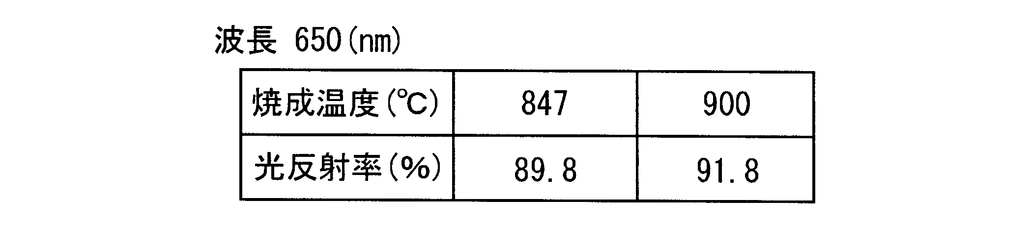
図6及び図7に示されるグラフ、並びに表1と表2に示されるデータから、セラミック層(5)から析出したガラスの結晶化度が3%より大きい場合、析出したガラスによって形成されるガラス層の表面での光反射率が高くなることがわかる。
図8は、上記発光デバイスの第1変形例を示す断面図である。図8に示す様に、上記発光デバイスにおいて、熱伝導部(4)の露出面(42)が枠体(3)の下方位置まで拡がって、該露出面(42)の周縁領域が枠体(3)によって覆われていてもよい。
第1変形例に係る発光デバイスによれば、キャビティ(30)の底面に隆起部が出現することが防止され、従ってキャビティ(30)の底面の高い平滑性が維持されることになる。
図9は、上記発光デバイスの第2変形例を示す断面図である。図9に示す様に、上記発光デバイスは、枠体(3)のない構成を有していてもよい。
図10は、上記発光デバイスの第3変形例を示す断面図である。図10に示す様に、上記発光デバイスにおいて、基体(2)の複数箇所に熱伝導部(4)を設け、各熱伝導部(4)の中央部を細くする一方、各熱伝導部(4)の上部及び下部を拡げて熱伝導部(4)~(4)の上部どうし及び下部どうしを連結させてもよい。本変形例に係る構成によれば、各熱伝導部(4)は、中央部が細くて且つ上部及び下部が拡がった形状を有することになる。よって、上記セラミック体形成工程において、各熱伝導部(4)を構成するビア(40)への熱伝導材(41)の充填が容易となる。
尚、本発明の各部構成は上記実施の形態に限らず、特許請求の範囲に記載の技術的範囲内で種々の変形が可能である。例えば、上記発光デバイスに採用したセラミック材、熱伝導材(41)等には、上記実施形態で説明した材料に限らず、種々の材料を用いることが出来る。
上記発光デバイスに採用した各種構成は、LED以外の発光素子を具えた発光デバイスにも適用することが可能である。又、上記発光デバイスに採用した各種構成は、発光素子を具えた発光デバイスに限らず、集積回路等、発熱する種々の電子素子を具えた電子デバイスにも適用することが可能である。
(1) LED(電子素子)
(10) パッケージ
(2) 基体
(21) 上面(表面)
(22) 下面(背面)
(3) 枠体
(30) キャビティ
(32) 樹脂材
(4) 熱伝導部
(40) ビア
(41) 熱伝導材
(42) 露出面
(5) セラミック層
(6) 金メッキ層
R1 設置領域
(10) パッケージ
(2) 基体
(21) 上面(表面)
(22) 下面(背面)
(3) 枠体
(30) キャビティ
(32) 樹脂材
(4) 熱伝導部
(40) ビア
(41) 熱伝導材
(42) 露出面
(5) セラミック層
(6) 金メッキ層
R1 設置領域
Claims (5)
- セラミック製の基体と、該基体の表面に搭載された電子素子と、該電子素子から発生した熱を基体の背面へ導く熱伝導部とを具え、該熱伝導部は、前記基体に開設されて該基体の表面から背面へ貫通するビアと、該ビアに充填された熱伝導材とから構成され、該熱伝導材が前記基体の表面に露出して前記熱伝導部の露出面が形成されており、該露出面上に前記電子素子が設置されている電子デバイスにおいて、
前記熱伝導部の露出面が前記電子素子の設置領域の外側まで拡がることにより、該電子素子の設置領域が、熱伝導部の露出面の周縁領域によって包囲されており、前記熱伝導部の露出面の内、前記電子素子の設置領域とは異なる領域がセラミック層により被覆されていることを特徴とする電子デバイス。 - 前記基体の表面に接合されて、前記電子素子を収容するためのキャビティを形成するセラミック製の枠体を更に具え、前記熱伝導部の露出面が前記枠体の下方位置まで拡がって、該露出面の周縁領域が前記枠体により覆われている請求項1に記載の電子デバイス。
- 前記電子素子は発光素子であって、前記セラミック層にはガラスが含有され、該ガラスの一部がセラミック層の表面に析出している請求項1又は請求項2に記載の電子デバイス。
- 前記セラミック層の表面に析出したガラスの結晶化度は3%より大きい請求項3に記載の電子デバイス。
- 前記基体は、前記熱伝導部を構成する熱伝導材との同時焼成が可能な低温同時焼成セラミックから形成されている請求項1乃至請求項4の何れかに記載の電子デバイス。
Applications Claiming Priority (2)
| Application Number | Priority Date | Filing Date | Title |
|---|---|---|---|
| JP2010-041292 | 2010-02-26 | ||
| JP2010041292A JP2012253048A (ja) | 2010-02-26 | 2010-02-26 | 電子デバイス |
Publications (1)
| Publication Number | Publication Date |
|---|---|
| WO2011104967A1 true WO2011104967A1 (ja) | 2011-09-01 |
Family
ID=44506403
Family Applications (1)
| Application Number | Title | Priority Date | Filing Date |
|---|---|---|---|
| PCT/JP2010/071442 Ceased WO2011104967A1 (ja) | 2010-02-26 | 2010-12-01 | 電子デバイス |
Country Status (2)
| Country | Link |
|---|---|
| JP (1) | JP2012253048A (ja) |
| WO (1) | WO2011104967A1 (ja) |
Families Citing this family (2)
| Publication number | Priority date | Publication date | Assignee | Title |
|---|---|---|---|---|
| JP6492443B2 (ja) * | 2014-07-28 | 2019-04-03 | Agc株式会社 | 発光素子用基板および発光装置 |
| US20210066159A1 (en) * | 2018-04-26 | 2021-03-04 | Kyocera Corporation | Heat dissipation board and electronic apparatus |
Citations (5)
| Publication number | Priority date | Publication date | Assignee | Title |
|---|---|---|---|---|
| JP2005197633A (ja) * | 2003-12-26 | 2005-07-21 | Samsung Electro Mech Co Ltd | 高出力発光ダイオードパッケージ及び製造方法 |
| JP2006066409A (ja) * | 2004-07-28 | 2006-03-09 | Kyocera Corp | 発光素子用配線基板および発光装置ならびに発光素子用配線基板の製造方法 |
| JP2006339559A (ja) * | 2005-06-06 | 2006-12-14 | Matsushita Electric Ind Co Ltd | Led部品およびその製造方法 |
| JP2007121613A (ja) * | 2005-10-27 | 2007-05-17 | Kyocera Corp | 光反射体、発光素子搭載用配線基板、および発光装置 |
| JP2009162950A (ja) * | 2007-12-28 | 2009-07-23 | Sumitomo Metal Electronics Devices Inc | 反射材およびそれを用いた反射体 |
-
2010
- 2010-02-26 JP JP2010041292A patent/JP2012253048A/ja active Pending
- 2010-12-01 WO PCT/JP2010/071442 patent/WO2011104967A1/ja not_active Ceased
Patent Citations (5)
| Publication number | Priority date | Publication date | Assignee | Title |
|---|---|---|---|---|
| JP2005197633A (ja) * | 2003-12-26 | 2005-07-21 | Samsung Electro Mech Co Ltd | 高出力発光ダイオードパッケージ及び製造方法 |
| JP2006066409A (ja) * | 2004-07-28 | 2006-03-09 | Kyocera Corp | 発光素子用配線基板および発光装置ならびに発光素子用配線基板の製造方法 |
| JP2006339559A (ja) * | 2005-06-06 | 2006-12-14 | Matsushita Electric Ind Co Ltd | Led部品およびその製造方法 |
| JP2007121613A (ja) * | 2005-10-27 | 2007-05-17 | Kyocera Corp | 光反射体、発光素子搭載用配線基板、および発光装置 |
| JP2009162950A (ja) * | 2007-12-28 | 2009-07-23 | Sumitomo Metal Electronics Devices Inc | 反射材およびそれを用いた反射体 |
Also Published As
| Publication number | Publication date |
|---|---|
| JP2012253048A (ja) | 2012-12-20 |
Similar Documents
| Publication | Publication Date | Title |
|---|---|---|
| JP6884823B2 (ja) | 電気素子搭載用パッケージ、アレイ型パッケージおよび電気装置 | |
| US8461755B2 (en) | Light source for lighting | |
| CN101853820A (zh) | 电子设备 | |
| CN101185174A (zh) | Led用基板以及led封装 | |
| TWI683458B (zh) | 用於高亮度發光裝置之周邊散熱配置 | |
| US9991434B2 (en) | Semiconductor device with metal-bonded heat dissipator and manufacturing method for the same | |
| JP6216789B2 (ja) | デバイス構造体 | |
| TWI769337B (zh) | 發光裝置 | |
| JP6034158B2 (ja) | 配線基板およびそれを用いた実装構造体 | |
| JP6010333B2 (ja) | 配線基板および電子装置 | |
| JP2012253048A (ja) | 電子デバイス | |
| JP2018517296A (ja) | キャリア要素を有する電子部品を製造する方法およびキャリア要素を有する電子部品 | |
| WO2011037185A1 (ja) | 実装用基板、発光体、および実装用基板の製造方法 | |
| JP5183965B2 (ja) | 照明装置の製造方法 | |
| JP4857709B2 (ja) | 発光装置 | |
| JP2013093341A (ja) | 電子デバイス | |
| KR101533068B1 (ko) | 인쇄 회로 기판 및 이를 구비하는 전자 소자 조립체 | |
| KR20100097017A (ko) | 발광소자용 패키지 및 그 제조방법 | |
| KR101211719B1 (ko) | 필름 타입의 광소자 패키지 및 그 제조 방법 | |
| JP5205806B2 (ja) | Ledチップ固定用基板およびその製造方法 | |
| JP2019114754A (ja) | 電子部品搭載用パッケージ、電子装置および電子モジュール | |
| JP2006181779A (ja) | セラミック基板の製造方法 | |
| JP6230795B2 (ja) | 光学素子用基板及び光学素子パッケージの製造方法 | |
| JP4926271B2 (ja) | 発光素子収納用パッケージおよび発光装置 | |
| JP6266369B2 (ja) | 発光素子搭載用セラミックパッケージ |
Legal Events
| Date | Code | Title | Description |
|---|---|---|---|
| 121 | Ep: the epo has been informed by wipo that ep was designated in this application |
Ref document number: 10846630 Country of ref document: EP Kind code of ref document: A1 |
|
| WWE | Wipo information: entry into national phase |
Ref document number: 1201000442 Country of ref document: TH |
|
| NENP | Non-entry into the national phase |
Ref country code: DE |
|
| 122 | Ep: pct application non-entry in european phase |
Ref document number: 10846630 Country of ref document: EP Kind code of ref document: A1 |
|
| NENP | Non-entry into the national phase |
Ref country code: JP |