WO2011104803A1 - プラズマ生成装置 - Google Patents
プラズマ生成装置 Download PDFInfo
- Publication number
- WO2011104803A1 WO2011104803A1 PCT/JP2010/007213 JP2010007213W WO2011104803A1 WO 2011104803 A1 WO2011104803 A1 WO 2011104803A1 JP 2010007213 W JP2010007213 W JP 2010007213W WO 2011104803 A1 WO2011104803 A1 WO 2011104803A1
- Authority
- WO
- WIPO (PCT)
- Prior art keywords
- gas supply
- gas
- plasma generation
- plasma
- supply plate
- Prior art date
- Legal status (The legal status is an assumption and is not a legal conclusion. Google has not performed a legal analysis and makes no representation as to the accuracy of the status listed.)
- Ceased
Links
Images





Classifications
-
- H—ELECTRICITY
- H05—ELECTRIC TECHNIQUES NOT OTHERWISE PROVIDED FOR
- H05H—PLASMA TECHNIQUE; PRODUCTION OF ACCELERATED ELECTRICALLY-CHARGED PARTICLES OR OF NEUTRONS; PRODUCTION OR ACCELERATION OF NEUTRAL MOLECULAR OR ATOMIC BEAMS
- H05H1/00—Generating plasma; Handling plasma
- H05H1/24—Generating plasma
- H05H1/46—Generating plasma using applied electromagnetic fields, e.g. high frequency or microwave energy
-
- C—CHEMISTRY; METALLURGY
- C23—COATING METALLIC MATERIAL; COATING MATERIAL WITH METALLIC MATERIAL; CHEMICAL SURFACE TREATMENT; DIFFUSION TREATMENT OF METALLIC MATERIAL; COATING BY VACUUM EVAPORATION, BY SPUTTERING, BY ION IMPLANTATION OR BY CHEMICAL VAPOUR DEPOSITION, IN GENERAL; INHIBITING CORROSION OF METALLIC MATERIAL OR INCRUSTATION IN GENERAL
- C23C—COATING METALLIC MATERIAL; COATING MATERIAL WITH METALLIC MATERIAL; SURFACE TREATMENT OF METALLIC MATERIAL BY DIFFUSION INTO THE SURFACE, BY CHEMICAL CONVERSION OR SUBSTITUTION; COATING BY VACUUM EVAPORATION, BY SPUTTERING, BY ION IMPLANTATION OR BY CHEMICAL VAPOUR DEPOSITION, IN GENERAL
- C23C16/00—Chemical coating by decomposition of gaseous compounds, without leaving reaction products of surface material in the coating, i.e. chemical vapour deposition [CVD] processes
- C23C16/44—Chemical coating by decomposition of gaseous compounds, without leaving reaction products of surface material in the coating, i.e. chemical vapour deposition [CVD] processes characterised by the method of coating
- C23C16/448—Chemical coating by decomposition of gaseous compounds, without leaving reaction products of surface material in the coating, i.e. chemical vapour deposition [CVD] processes characterised by the method of coating characterised by the method used for generating reactive gas streams, e.g. by evaporation or sublimation of precursor materials
- C23C16/452—Chemical coating by decomposition of gaseous compounds, without leaving reaction products of surface material in the coating, i.e. chemical vapour deposition [CVD] processes characterised by the method of coating characterised by the method used for generating reactive gas streams, e.g. by evaporation or sublimation of precursor materials by activating reactive gas streams before their introduction into the reaction chamber, e.g. by ionisation or addition of reactive species
-
- C—CHEMISTRY; METALLURGY
- C23—COATING METALLIC MATERIAL; COATING MATERIAL WITH METALLIC MATERIAL; CHEMICAL SURFACE TREATMENT; DIFFUSION TREATMENT OF METALLIC MATERIAL; COATING BY VACUUM EVAPORATION, BY SPUTTERING, BY ION IMPLANTATION OR BY CHEMICAL VAPOUR DEPOSITION, IN GENERAL; INHIBITING CORROSION OF METALLIC MATERIAL OR INCRUSTATION IN GENERAL
- C23C—COATING METALLIC MATERIAL; COATING MATERIAL WITH METALLIC MATERIAL; SURFACE TREATMENT OF METALLIC MATERIAL BY DIFFUSION INTO THE SURFACE, BY CHEMICAL CONVERSION OR SUBSTITUTION; COATING BY VACUUM EVAPORATION, BY SPUTTERING, BY ION IMPLANTATION OR BY CHEMICAL VAPOUR DEPOSITION, IN GENERAL
- C23C16/00—Chemical coating by decomposition of gaseous compounds, without leaving reaction products of surface material in the coating, i.e. chemical vapour deposition [CVD] processes
- C23C16/44—Chemical coating by decomposition of gaseous compounds, without leaving reaction products of surface material in the coating, i.e. chemical vapour deposition [CVD] processes characterised by the method of coating
- C23C16/50—Chemical coating by decomposition of gaseous compounds, without leaving reaction products of surface material in the coating, i.e. chemical vapour deposition [CVD] processes characterised by the method of coating using electric discharges
- C23C16/505—Chemical coating by decomposition of gaseous compounds, without leaving reaction products of surface material in the coating, i.e. chemical vapour deposition [CVD] processes characterised by the method of coating using electric discharges using radio frequency discharges
- C23C16/509—Chemical coating by decomposition of gaseous compounds, without leaving reaction products of surface material in the coating, i.e. chemical vapour deposition [CVD] processes characterised by the method of coating using electric discharges using radio frequency discharges using internal electrodes
-
- H—ELECTRICITY
- H01—ELECTRIC ELEMENTS
- H01J—ELECTRIC DISCHARGE TUBES OR DISCHARGE LAMPS
- H01J37/00—Discharge tubes with provision for introducing objects or material to be exposed to the discharge, e.g. for the purpose of examination or processing thereof
- H01J37/32—Gas-filled discharge tubes
- H01J37/32009—Arrangements for generation of plasma specially adapted for examination or treatment of objects, e.g. plasma sources
- H01J37/32082—Radio frequency generated discharge
- H01J37/321—Radio frequency generated discharge the radio frequency energy being inductively coupled to the plasma
-
- H—ELECTRICITY
- H01—ELECTRIC ELEMENTS
- H01J—ELECTRIC DISCHARGE TUBES OR DISCHARGE LAMPS
- H01J37/00—Discharge tubes with provision for introducing objects or material to be exposed to the discharge, e.g. for the purpose of examination or processing thereof
- H01J37/32—Gas-filled discharge tubes
- H01J37/32431—Constructional details of the reactor
- H01J37/3244—Gas supply means
Definitions
- the present invention relates to a plasma generation apparatus for forming, for example, a thin film transistor (TFT) constituting a liquid crystal display device.
- TFT thin film transistor
- a crystalline thin film such as a silicon thin film is formed on a substrate. Yes.
- the plasma CVD (Chemical Vapor Deposition) method is known as a method for forming a semiconductor film or the like using plasma, and is integrated. It is used for the production of circuits, liquid crystal display panels, organic electroluminescence elements, solar cells and the like.
- a plasma CVD apparatus for forming a film by using this plasma CVD method includes a flat cathode electrode and a flat anode electrode arranged so as to face each other inside a processing chamber.
- the anode electrode is provided in a substrate holder disposed on the upper wall of the processing chamber, and a deposition substrate such as a glass substrate is mounted on the surface on the cathode electrode side by the substrate holder. .
- the cathode electrode has a plurality of gas inlets formed on the anode electrode side for introducing a raw material gas for film formation into the processing chamber. Note that the cathode electrode is disposed in parallel to the deposition target substrate.
- the source gas is introduced into the processing chamber from each gas inlet, and the cathode electrode and the anode electrode By applying a voltage between the two, a plasma state of the source gas is generated as a glow discharge phenomenon by dielectric breakdown of the generated electric field.
- dissociation of the source gas gas molecules
- radicals are generated in the cathode sheath portion where the relatively strong electric field is formed in the vicinity of the cathode electrode and in the vicinity thereof.
- the radicals generated in this way diffuse to the substrate to be processed and deposit on the surface of the substrate, thereby forming a thin film.
- the defect rate of the microcrystalline silicon or polycrystalline silicon is reduced, and the deposition rate is increased. From the viewpoint of improvement, it is necessary to set the pressure in the processing chamber (chamber) of the plasma CVD apparatus to a high pressure.
- the anode electrode that is, the processing target substrate
- the distance between the cathode electrodes it is necessary to set the distance between the cathode electrodes to a predetermined distance (for example, 10 mm) or less.
- a plasma CVD apparatus for ensuring the uniformity (parallelism) of the distance between electrodes. More specifically, the cathode electrode in which the gas introduction port is formed is attached to the reaction chamber container from the outside by a coupling means via an insulating member disposed on the outer wall around the cathode electrode receiving opening surface of the reaction container.
- a plasma CVD apparatus has been proposed in which an outer wall of a reaction vessel and an insulating member, and an insulating member and a cathode electrode are hermetically sealed by an O-ring.
- the parallelism between the gas introduction surface of the cathode electrode and the deposition target substrate (that is, the anode electrode) is adjusted by controlling the flatness ratio due to the elastic deformation of the O-ring by the coupling means. It has a configuration (see, for example, Patent Document 1).
- a method of generating inductively coupled plasma using high frequency power is known from the viewpoint of obtaining a plasma with a density as high as possible in the plasma generation chamber.
- a high frequency antenna is provided for the plasma generation chamber, and the high frequency antenna is used for the gas introduced into the room. By applying high frequency power, inductively coupled plasma is generated.
- the high frequency antenna is arranged inside the plasma generation chamber from the viewpoint of improving the utilization efficiency of the high frequency power supplied.
- the high-frequency antenna disposed inside the plasma generation chamber is formed of a conductive member (conductive tube) formed of a conductive material such as aluminum and an insulating material such as quartz. It is comprised by the insulating member (insulating tube) provided so that the surface might be coat
- the gas introducing chamber is formed on the ceiling wall of the plasma generating container formed inside and spaced apart from the high frequency antenna. It is configured to generate inductively coupled plasma by applying high frequency power from a high frequency antenna to the film forming gas introduced into the room through the mouth (see, for example, Patent Document 2).
- the plasma CVD apparatus described in Patent Document 1 has a problem that only the peripheral portion of the cathode electrode can be controlled even when the coupling means is used. Further, since the plasma CVD apparatus described in Patent Document 1 uses a flat electrode, when the apparatus size is increased, the size of the electrode increases and the heat capacity of the electrode also increases. As a result, the electrode is deformed and warped due to heat at the time of plasma generation, and the electrode is bent or distorted.
- the distance between the anode electrode and the cathode electrode becomes non-uniform due to the above-described deflection and distortion of the electrode, resulting in non-uniform discharge and a large area (for example, a width of 2160 mm and a length of 2460 mm). It becomes difficult to generate plasma uniformly in the plasma region formed between the electrodes having the. As a result, there is a problem that it is difficult to form a thin film having a uniform film thickness on the surface of the substrate to be processed.
- the present invention has been made in view of the above-described problems, and generates a uniform discharge without being affected by heat during plasma generation, and has a uniform film thickness on the surface of the substrate to be processed. It is an object of the present invention to provide a plasma generation apparatus capable of forming a thin film and performing maintenance efficiently.
- a plasma generation apparatus includes a plasma generation container having a plasma generation chamber formed therein, a holder provided inside the plasma generation chamber, and for holding a deposition target substrate.
- a gas supply plate provided inside the plasma generation chamber and having a gas introduction port for introducing a film formation gas and a gas supply port for supplying the introduced film formation gas into the plasma generation chamber; It is equipped with a high-frequency antenna that is provided inside and generates inductively coupled plasma by applying high-frequency power to the deposition gas.
- the high-frequency antenna and gas supply plate are integrated as a unit, and the unit generates plasma. It is configured to be detachable from the container.
- a high-frequency antenna that generates high-frequency power by applying high-frequency power to the deposition gas is provided inside the plasma generation chamber.
- a plurality of high frequency antennas may be provided.
- the heat capacity of each high-frequency antenna is smaller than the heat capacity of a plate-like electrode in a conventional plasma CVD apparatus, it is possible to effectively suppress the occurrence of deformation due to heat during plasma generation. Therefore, since plasma can be generated uniformly in the plasma generation chamber, a thin film having a uniform film thickness can be formed on the surface of the deposition target substrate.
- the high-frequency antenna and the gas supply member are integrated as one unit, and the unit is configured to be detachable from the plasma generation vessel. Therefore, for example, when performing maintenance of a gas inlet (for example, replacement of a damaged gas inlet), maintenance is performed only for a unit including a gas supply member in which the gas inlet is formed (that is, replacement of one unit). Therefore, unlike the above-described prior art parallel plate electrode type plasma CVD apparatus, it is not necessary to replace the electrodes that serve both as the antenna and the gas supply system when performing maintenance. Therefore, it becomes possible to improve the maintenance efficiency and to reduce the cost for performing maintenance.
- the area of one unit in which the high-frequency antenna and the gas supply member are integrated can be reduced, so that high processing accuracy is achieved. It becomes unnecessary, and workability can be improved.
- the gas supply port is formed in the gas supply member, it is necessary to ensure a uniform gas supply distribution in a large area in order to improve the film thickness and film quality uniformity in a large area. Even so, the number of gas introduction ports provided in the plasma generation container can be minimized, and a large number of gas supply ports can be formed in the gas supply member without reducing the strength of the plasma generation container. It becomes possible. Therefore, the gas supply ports can be formed with high accuracy and high density as compared with the conventional internal antenna type plasma CVD apparatus. As a result, when the deposition gas is supplied from the gas supply port to the plasma generation chamber, the supply distribution of the deposition gas can be improved, so that the thickness and quality of the film formed on the deposition target substrate can be improved. Uniformity can be improved.
- a uniform gas supply distribution can be obtained in a large area by changing the size of the small gas shower unit.
- the plasma generation apparatus of the present invention may have a configuration in which a plurality of units are arranged.
- the high frequency antenna may be provided with a cooling pipe for a high frequency antenna for introducing cooling water for cooling the high frequency antenna.
- the gas supply plate may be provided with a gas supply plate cooling pipe for introducing cooling water for cooling the gas supply plate.
- the plasma generation apparatus of the present invention may further include a gas introduction pipe that is connected to the gas supply plate and introduces the film forming gas into the gas supply plate.
- a plurality of the gas supply ports may be arranged to form a honeycomb arrangement.
- the gas supply port can be continuously provided in the gas supply member, so that the gas supply distribution can be further improved.
- the uniformity of the film thickness and film quality of the film formed on the deposition target substrate can be further improved.
- the plasma generation apparatus of the present invention has an excellent characteristic that a thin film having a uniform film thickness can be formed on the surface of the deposition target substrate and maintenance efficiency can be improved. Therefore, the present invention is preferably used in a plasma generating apparatus in which the film forming gas is a silane-based gas. With such a structure, a silicon thin film used for a solar cell or the like is uniformly formed on the surface of the film forming substrate. A plasma generation apparatus which can be formed as a thin film having a thickness can be provided.
- the present invention it is possible to form a thin film having a uniform film thickness on the surface of the deposition target substrate without being affected by heat during plasma generation. In addition, it is possible to improve maintenance efficiency and reduce costs when performing maintenance.
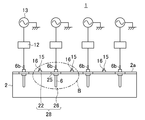
- FIG. 1 is a schematic diagram showing an overall configuration of a plasma generation apparatus according to a first embodiment of the present invention. It is the schematic which shows the whole structure of the plasma production
- FIG. 5 is a DD cross-sectional view of FIG. 4.
- FIG. 4 is a DD cross-sectional view of FIG. 4.
- FIG. 6 is a plan view for explaining the arrangement of units shown in FIG. 5 in the plasma generating apparatus according to the first embodiment of the present invention. It is a figure for demonstrating the unit with which the antenna unit and gas supply member of the plasma production apparatus which concern on the 2nd Embodiment of this invention were integrated. It is a top view for demonstrating the modification of the gas supply member of the plasma generation apparatus which concerns on embodiment of this invention. It is sectional drawing for demonstrating the modification of the gas supply port formed in the gas supply member of the plasma production apparatus which concerns on embodiment of this invention. It is sectional drawing for demonstrating the modification of the gas supply port formed in the gas supply member of the plasma production apparatus which concerns on embodiment of this invention. It is sectional drawing for demonstrating the modification of the gas supply port formed in the gas supply member of the plasma production apparatus which concerns on embodiment of this invention. It is sectional drawing for demonstrating the modification of the gas supply port formed in the gas supply member of the plasma production apparatus which concerns on embodiment of this invention.
- FIG. 1 is a schematic diagram showing the overall configuration of the plasma generating apparatus according to the first embodiment of the present invention
- FIG. 2 is a schematic diagram showing the overall configuration of the plasma generating apparatus according to the first embodiment of the present invention. It is a figure and is a figure at the time of seeing FIG. 1 from the direction of arrow A.
- FIG. 3 is a view for explaining a unit in which the antenna unit and the gas supply plate of the plasma generating apparatus according to the first embodiment of the present invention are integrated, and is an enlarged cross section of a portion B in FIG.
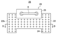
- FIG. 4 is a plan view showing a unit in which the antenna unit and the gas supply plate of the plasma generating apparatus according to the first embodiment of the present invention are integrated.
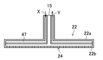
- 5 is a sectional view taken along the line DD of FIG. 4
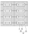
- FIG. 6 is a plan view for explaining the arrangement of the units shown in FIG. 4 in the plasma generating apparatus according to the first embodiment of the present invention. It is.
- a plasma generation apparatus (plasma CVD apparatus) 1 includes a plasma generation container 2 in which a plasma generation chamber (film formation chamber) 3 is formed.
- the plasma generation container 2 is made of, for example, a metal such as aluminum or SUS.
- a holder 5 which is a holding member for holding the deposition target substrate 4 is installed in the lower part of the plasma generation chamber 3.
- the holder 5 is made of a material such as aluminum or SUS, for example. It is also possible to use those aluminum or SUS sprayed with alumina.
- the holder 5 may be configured to incorporate a heater (not shown) for heating the deposition target substrate 4.
- a plurality (eight in the present embodiment) of high-frequency antennas 6 are inserted and installed from the ceiling wall 2a of the plasma generating container 2 into the plasma generating chamber 3.
- the high-frequency antenna 6 is for generating high-frequency power by applying high-frequency power to the film forming gas supplied into the plasma generation chamber 3, and facing the holder 5 inside the plasma generation chamber 3. Is provided.
- each of the plurality of high-frequency antennas 6 has the same size, and is arranged adjacent to each other at a predetermined interval on the same plane.
- the high-frequency antenna 6 has a substantially U-shaped cross section, and is attached to a base portion 25 as an attachment member as shown in FIGS. 1 and 2.
- the base portion 25 is integrated as an antenna unit 26.
- the high-frequency antenna 6 is insulated from the base portion 25 by an insulating material, and is fixed to the base portion 25 by a fixing member (not shown) such as a bolt.
- the base portion 25 having a substantially rectangular cross section is shown.
- the shape of the base portion 25 is not particularly limited.
- a base portion 25 having a square or substantially elliptical cross section can be used.
- a portion of the conductor 10 constituting the high frequency antenna 6 that protrudes from the ceiling wall 2 a of the plasma generation container 2 toward the outside of the plasma generation chamber 3 is the portion of the high frequency antenna 6. Terminal portions 6a and 6b are configured.
- one terminal part 6b is connected to the matching box 12 among the terminal parts 6a and 6b of the high frequency antenna 6 protruding toward the outside of the plasma generation chamber 3, and the terminal part 6b is It is connected to the high frequency power supply 13 through the matching box 12.
- each high-frequency antenna 6 is grounded. Moreover, each high frequency antenna 6 becomes a structure connected in parallel by the terminal part 6b.
- a gas supply plate 22 which is a gas supply member having a hollow structure, is provided on the plasma generation chamber 3 side of the ceiling wall 2 a of the plasma generation container 2.
- a predetermined film forming gas supplied into the plasma generation chamber 3 is applied to the ceiling wall 2 a side 22 a of the plasma generation container 2 of the gas supply plate 22.
- a gas inlet 15 for introduction into the gas supply plate 22 is formed.
- the gas inlet 15 has a circular tube shape and is provided so as to protrude from the ceiling wall 2 a side 22 a of the plasma generation container 2.
- the film forming gas is introduced into each of the plurality of gas supply plates 22 provided in the plasma generation chamber 3.
- a film forming gas introduced into the gas supply plate 22 is supplied to the plasma generation chamber 2 on the plasma generation chamber 3 side 22 b of the gas supply plate 22.
- the gas supply port 24 is formed.
- the gas introduced into the gas supply plate 22 from the gas introduction port 15 is supplied into the plasma generation chamber 3 from the gas supply port 24 as indicated by an arrow. Yes.
- the shape of the gas supply port 24 is not particularly limited as long as the film forming gas can be supplied into the plasma generation chamber 3, but from the viewpoint of excellent workability, the present embodiment. 4 and 5, a gas supply port 24 having a substantially cylindrical shape with a substantially circular plane and a substantially rectangular cross section is provided.
- a metal terminal 16 such as a vacuum joint is provided on the ceiling wall 2 a of the plasma generation container 2, and the gas inlet 15 is connected to the ceiling wall 2 a and the metal terminal of the plasma generation container 2.
- the gas introduction port 15 is installed from the ceiling wall 2 a of the plasma generation container 2 into the plasma generation chamber 3 by being inserted into the plasma generation chamber 2.
- the O-ring 17 provided between the gas inlet 15 and the ceiling wall 2 a of the plasma generation container 2 is used to seal the gas inlet 15 and the ceiling wall 2 a of the plasma generation container 2. Is secured.
- the potential of the base portion 25 constituting the antenna unit 26 described above may be a ground potential, and since it is not necessary to ensure insulation between the plasma generation container 2, a fixing member (not shown) such as a bolt is used.
- the antenna unit is arranged inside the plasma generation chamber 3 by fixing the base portion 25 to the ceiling wall 2 a of the plasma generation container 2.
- the gas supply plate 22 is provided with a gas supply plate cooling pipe 47 (hereinafter referred to as “pipe 47”) for introducing cooling water for cooling the gas supply plate 22. .
- the cooling water is supplied to the pipe 47 from the direction of the arrow X in the drawing, introduced into the gas supply plate 22, and discharged from the direction of the arrow Y in the drawing to the outside of the gas supply plate 22.
- the high-frequency antenna 6 is provided with a high-frequency antenna cooling pipe 48 (hereinafter referred to as “pipe 48”) for introducing cooling water for cooling the high-frequency antenna 6 as shown in FIG. Yes.
- the cooling water is supplied from the direction of the high frequency antenna 6 to the pipe 48 and introduced into the high frequency antenna 6, and then discharged to the outside of the high frequency antenna 6.
- a gas containing an element constituting a thin film to be formed on the deposition target substrate 4 is used as the deposition gas introduced through the gas inlet 15.
- silane SiH 4
- a silane-based gas such as hydrogen diluted silane (SiH 4 / H 2 ) is used.
- a mixed gas of a raw material gas and a rare gas (inert gas) such as argon gas, helium gas, neon gas, krypton gas, or xenon gas may be introduced into the plasma generation container 2.
- the film formation substrate 4 can be irradiated simultaneously with the ions of the elements constituting the source gas and the ions of the rare gas. Moreover, since the rare gas ions do not constitute a thin film, the crystallization of the thin film can be promoted by the kinetic energy of the rare gas ions.
- the plasma generator 1 exhausts gas from the gas inlet 15 and the plasma generation chamber 3 to set the inside of the plasma generation chamber 3 to a predetermined plasma generation pressure.
- the vacuum pump 14 is provided.
- the vacuum pump 14 is connected to the plasma generation vessel 2 via a pipe 32 having a gate valve 31 as shown in FIG.
- the gas in the gas inlet 15 and the plasma generation chamber 3 is exhausted to the outside through the pipe 32 by opening the gate valve 31.
- the film formation substrate 4 is placed on the holder 5 provided inside the plasma generation chamber 3, and the film formation substrate 4 is held by the holder.
- a predetermined film forming gas for example, silane-based gas
- the inside of the plasma generation chamber 3 is maintained at the film forming pressure.
- high-frequency power is applied to the high-frequency antenna 6 from the high-frequency power source 13 through the matching box 12, thereby generating high-frequency discharge in the plasma generation chamber 3 and forming a film in the plasma generation chamber 3.
- the gas is ionized (excited) to generate inductively coupled plasma.
- a film (for example, a silicon film) is formed (deposited) on the deposition target substrate 4 on the holder 5 by the inductively coupled plasma.
- the frequency of the high frequency power is, for example, 13.56 MHz (when a silicon film is formed), 50 MHz, 60 MHz, or the like.
- the high-frequency antenna 6 that generates high-frequency power by applying high-frequency power to the deposition gas is used inside the plasma generation chamber 3. Therefore, even when the apparatus size is increased, a plurality of high-frequency antennas 6 may be provided as shown in FIGS. 1, 2, and 6, and the plate-like shape in the conventional plasma CVD apparatus is used. Since the heat capacity of each high-frequency antenna 6 is smaller than the heat capacity of the electrodes, it is possible to effectively suppress the occurrence of deformation due to heat at the time of plasma generation.
- segmenting an electrode and unitizing can be considered.
- flat electrodes arranged in parallel are used, it is considered difficult to divide the electrodes into units due to the influence of high-frequency power disturbances at the joints between the units.
- the antenna unit 26 that is, the high frequency antenna 6
- the gas supply plate 22 are integrated as one unit 28, and the unit 28 is characterized in that it is configured to be detachable from the plasma generation vessel 2.
- the gas inlet 15 of the gas supply plate 22 is connected to the ceiling of the plasma generation container 2 from the inside (plasma generation chamber 3 side) of the plasma generation container 2.
- the terminal portions 6 a and 6 b of the high-frequency antenna 6 constituting the antenna unit 26 are inserted into the ceiling wall 2 a of the plasma generation vessel 2.
- the unit 28 mounted on the ceiling wall 2a of the plasma generation vessel 2 is moved together with the unit 28 from the ceiling wall 2a side of the plasma generation vessel 2 to the plasma generation chamber 3 side.
- each unit 28 in which the high-frequency antenna 6 and the gas supply plate 22 are integrated can be reduced as compared with the large-area electrode that serves both as the conventional antenna and the gas supply system. A high degree of machining accuracy is not required, and the workability can be improved.
- the gas supply port 24 is formed in the gas supply plate 22, in order to improve the film thickness and film quality uniformity in a large area, Even when it is necessary to ensure a uniform gas supply distribution, the number of gas inlets 15 provided in the plasma generation vessel 2 can be minimized. Accordingly, a large number of gas supply ports 24 can be formed in the gas supply plate 22 without reducing the strength of the plasma generation container 2. As a result, the gas supply ports 24 can be formed with high precision and high density as compared with the above-described conventional internal antenna type plasma CVD apparatus. Accordingly, when the film forming gas is supplied from the gas supply port 24 into the plasma generation chamber 3, the supply distribution of the film forming gas can be improved.
- the antenna unit 26 and the gas supply plate 22 are integrated as one unit 28, even when a plurality of units 28 are arranged in the plasma generation chamber 3, the high-frequency antennas constituting each unit 28
- the power supply amount can be controlled every 6 and the film formation gas supply amount can be controlled for each gas supply plate 22 constituting each unit 28. Therefore, it is possible to precisely control the film thickness and film quality of the film formed on the deposition target substrate 4.
- a high-frequency antenna 6 that generates high-frequency power by applying high-frequency power to the deposition gas is used inside the plasma generation chamber 3. Therefore, even when the apparatus size is increased, a plurality of high-frequency antennas 6 may be provided, and since the heat capacity of each high-frequency antenna 6 is small, generation of deformation due to heat during plasma generation is effective. Can be suppressed. Accordingly, since it is possible to generate plasma uniformly in the plasma generation chamber 3, a thin film having a uniform film thickness can be formed on the surface of the deposition target substrate 4.
- the antenna unit 26 and the gas supply plate 22 are integrated as a single unit 28. Further, the unit 28 is configured to be detachable from the plasma generation container 2. Accordingly, when the maintenance of the gas inlet 15 is performed, the maintenance can be performed only for the unit 28 including the gas supply plate 22 in which the gas inlet 15 is formed. Unlike the plasma CVD apparatus, when performing maintenance, it is not necessary to replace the entire electrode that serves both as an antenna and a gas supply system. Therefore, it becomes possible to improve the maintenance efficiency and to reduce the cost for performing maintenance.
- each unit 28 in which the high-frequency antenna 6 and the gas supply plate 22 are integrated can be reduced as compared with the above-mentioned conventional antenna and gas electrode. Therefore, a high degree of processing accuracy is not required, and the workability can be improved.
- the gas supply port 24 is formed in the gas supply plate 22. Accordingly, a large number of gas supply ports 24 can be formed in the gas supply plate 22 without reducing the strength of the plasma generation container 2. Therefore, since the gas supply ports 24 can be formed with high accuracy and high density, the supply distribution of the film formation gas can be improved when the film formation gas is supplied from the gas supply port 24 into the plasma generation chamber 3. Can be planned. As a result, the film thickness and film quality uniformity of the film formed on the deposition target substrate 4 can be improved.
- the plasma generation apparatus 1 having a desired antenna arrangement can be constructed in accordance with the type and size of the deposition target substrate 4.
- the high frequency antenna 6 is provided with a pipe 48 for introducing cooling water for cooling the high frequency antenna 6. Therefore, it becomes possible to more effectively suppress the deformation of the high-frequency antenna 6 caused by the heat at the time of plasma generation.
- the gas supply plate 22 is provided with a pipe 47 for introducing cooling water for cooling the gas supply plate 22. Therefore, it is possible to effectively suppress deformation of the gas supply plate 22 due to heat at the time of plasma generation.
- FIG. 7 is a view for explaining a unit in which an antenna unit and a gas supply plate of a plasma generating apparatus according to a second embodiment of the present invention are integrated, and is an enlarged cross-sectional view of a portion B in FIG.
- FIG. 4 is a view corresponding to (that is, corresponding to FIG. 3 of the first embodiment). Note that the same components as those in the first embodiment are denoted by the same reference numerals, and description thereof is omitted.
- the overall configuration of the plasma generation apparatus, the overall configuration of the antenna unit of the plasma generation apparatus, and the overall configuration of the unit in which the antenna unit and the gas supply plate are integrated have been described in the first embodiment. The detailed description is omitted here.
- the gas introduction pipe 45 is inserted into the plasma production chamber 3 from the side wall 2b of the plasma production vessel 2, and a plurality of gas introduction pipes 45 are connected by joints 46 to form plasma.
- the plasma generation container 2 is arranged between the ceiling wall 2 a and the unit 28.
- gas introduction tube 45 may be inserted into the plasma generation chamber 3 from the ceiling wall 2 a of the plasma generation container 2.
- the gas inlet 15 provided in each gas supply plate 22 and the joint 46 are connected, and the gas inlet pipe 45 and the gas inlet 15 are connected via the joint 46. It is the composition which becomes.
- the gas introduced into the gas supply plate 22 from the gas introduction pipe 45 through the joint 46 is plasma from the gas supply port 24 formed in the gas supply plate 22. It is configured to be supplied into the generation chamber 3.
- the gas supply plate 22 is provided with a gas supply plate cooling pipe 49 (hereinafter referred to as a cooling pipe 49 for introducing the cooling water for cooling the gas supply plate 22). , Referred to as “pipe 49”). As shown in FIG. 7, the pipe 49 is provided on the ceiling wall 2 a side 22 a of the plasma generation container 2 of the gas supply plate 22.
- a part 49 a of the pipe 49 protrudes outward from the side wall 2 b of the plasma generation container 2, and the cooling water is supplied from the part 49 a of the pipe 49.
- it is supplied to the pipe 49 from the direction of the arrow X in the drawing, introduced into the surface of the gas supply plate 22, and discharged from the direction of the arrow Y in the drawing to the outside of the gas supply plate 22.
- cooling structure of the high-frequency antenna 6 is the same as that of the first embodiment.
- the gas introduction pipe 45 is provided. Therefore, unlike the first embodiment, there is no need to insert the gas introduction port 15 into the ceiling wall 2a of the plasma generation vessel 2, so that the gas introduction port 15 and the ceiling wall 2a of the plasma generation vessel 2 are separated from each other. There is no need to ensure airtightness. Therefore, it is possible to effectively maintain the degree of vacuum in the plasma generation container 2 as compared with the first embodiment.
- the gas supply port 24 having a substantially circular plane is provided.
- the plane is polygonal (hexagonal in FIG. 8).
- a plurality of gas supply ports 24 having a substantially polygonal column shape may be provided, and the plurality of gas supply ports 24 may be arranged in a honeycomb arrangement.
- the gas supply ports 24 can be continuously provided without gaps, so that the gas supply distribution can be further improved, and as a result, the film formed on the deposition target substrate 4 can be improved. The uniformity of film thickness and film quality can be further improved.
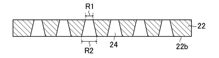
- FIGS. 9 and 10 a configuration may be provided in which the gas supply port 24 having the cross-sectional shape shown in FIGS. That is, as shown in FIG. 9, gas supply ports 24 having different inner diameters R1, R2 (R1 ⁇ R2) may be provided. Moreover, as shown in FIG. 10, it is good also as a structure which provides the gas supply port 24 which has a cross-sectional taper shape. Furthermore, as shown in FIG. 11, a gas supply port 24 in which a hole having a substantially columnar shape and a hole having a tapered shape are combined may be provided. Note that when the gas supply plate 22 shown in FIGS. 9 to 11 is arranged, the ceiling wall 2a side and the plasma generation chamber 3 side 22b of the plasma generation container 2 can be replaced with each other.
- a plasma generation device for forming a thin film transistor (TFT) constituting a liquid crystal display device.
- TFT thin film transistor
Landscapes
- Chemical & Material Sciences (AREA)
- Engineering & Computer Science (AREA)
- Physics & Mathematics (AREA)
- Plasma & Fusion (AREA)
- Chemical Kinetics & Catalysis (AREA)
- General Chemical & Material Sciences (AREA)
- Analytical Chemistry (AREA)
- Materials Engineering (AREA)
- Mechanical Engineering (AREA)
- Metallurgy (AREA)
- Organic Chemistry (AREA)
- Electromagnetism (AREA)
- Spectroscopy & Molecular Physics (AREA)
- Chemical Vapour Deposition (AREA)
- Plasma Technology (AREA)
Abstract
プラズマ生成装置(1)は、プラズマ生成室(3)が内部に形成されたプラズマ生成容器(2)と、プラズマ生成室(3)の内部に設けられ、成膜ガスを導入するガス導入口(15)と導入された成膜ガスをプラズマ生成室(3)内へ供給するガス供給口(24)とが形成されたガス供給板(22)と、プラズマ生成室(3)の内部に設けられ、成膜ガスに高周波電力を印加して誘導結合型のプラズマを生成する高周波アンテナ(6)とを備える。そして、高周波アンテナ(6)とガス供給板(22)とがユニット(28)として一体化されており、ユニット(28)が、プラズマ生成容器(2)に対して着脱自在に構成されている。
Description
本発明は、例えば、液晶表示装置を構成する薄膜トランジスタ(TFT)を形成するためのプラズマ生成装置に関する。
液晶表示装置を構成する薄膜トランジスタ(TFT)、半導体集積回路、太陽電池等の各種半導体デバイスを製造するために、基材上に結晶性を有する薄膜、例えば、シリコン薄膜を形成することが行われている。
また、このような半導体デバイスを製造する方法として、ガスプラズマを利用して膜形成を行うプラズマ生成装置を使用した方法が提案されている。
このガスプラズマを発生させる方法は種々の方法が知られているが、そのうち、プラズマCVD(Chemical Vapor Deposition)法は、プラズマを利用して半導体膜等を成膜する方法として知られており、集積回路、液晶表示パネル、有機エレクトロルミネッセンス素子及び太陽電池等の製造に使用されている。
このプラズマCVD法を用いて成膜を行うためのプラズマCVD装置は、処理室の内部に互いに対向するように配置された平板状のカソード電極及び平板状のアノード電極を備えている。
例えば、アノード電極は、処理室の上壁部に配置された基板ホルダー内に設けられ、当該基板ホルダーによってカソード電極側の表面にガラス基板等の被成膜基板が装着される構成となっている。
また、カソード電極には、成膜用の原料ガスを処理室内に導入するための複数のガス導入口がアノード電極側に形成されている。なお、カソード電極は、被成膜基板に平行となるように配置される。
このプラズマCVD装置では、アノード電極上に被処理基板を装着して真空ポンプ等で処理室の内部を減圧した状態で、各ガス導入口から原料ガスを処理室内に導入し、カソード電極とアノード電極との間に電圧を印加することにより、発生した電界の絶縁破壊によってグロー放電現象として原料ガスのプラズマ状態を生じさせる。これにより、カソード電極の近傍において比較的強い電界が形成されるカソードシース部やその付近では、原料ガス(気体分子)の解離が促進されてラジカルが生成される。そして、このように生成されたラジカルが、被処理基板にまで拡散し、その基板表面に堆積することにより、薄膜が成膜される。
ここで、一般に、太陽電池等で使用される微結晶シリコンや多結晶シリコン等の薄膜をプラズマCVD装置により形成する場合、微結晶シリコンや多結晶シリコンの欠陥性を低下させるとともに、成膜速度を向上させるとの観点から、プラズマCVD装置の処理室(チャンバー)内の圧力を高圧に設定する必要がある。
また、このような高い圧力に設定された処理室内でプラズマを発生させて、被成膜基板とカソード電極間のプラズマ放電を適切に維持するとの観点から、アノード電極(即ち、被処理基板)とカソード電極間の距離を所定の距離(例えば、10mm)以下に設定する必要がある。
また、平板状の電極間距離(即ち、アノード電極とカソード電極との間の距離)の変動率が大きくなると、反応ガス流やプラズマ放電における不均一性が大きくなり、被成膜基板の表面において、均一な薄膜分布を得ることが困難になる。
そこで、電極間距離の均一性(平行性)を確保するためのプラズマCVD装置が提案されている。より具体的には、ガス導入口が形成されたカソード電極を、反応容器のカソード電極受入開口面の周囲の外壁に配置された絶縁部材を介して、結合手段によって反応室容器へ外側から装着し、反応容器の外壁と絶縁部材との間、及び絶縁部材とカソード電極との間をOリングによって気密シールしたプラズマCVD装置が提案されている。そして、このプラズマCVD装置においては、Oリングの弾性変形による偏平率を結合手段で制御することによって、カソード電極のガス導入面と被成膜基板(即ち、アノード電極)との平行性を調節する構成となっている(例えば、特許文献1参照)。
また、プラズマ生成室内において、できるだけ高密度で均一なプラズマを得るとの観点から、高周波電力を用いて誘導結合プラズマを発生させる方法が知られている。
この誘導結合プラズマを発生させるプラズマ生成装置においては、高密度で均一なプラズマを得るために、プラズマ生成室に対して高周波アンテナを設けるとともに、この高周波アンテナにより、室内に導入されたガスに対して高周波電力を印加することにより、誘導結合プラズマを生成する構成となっている。
また、高周波アンテナは、投入される高周波電力の利用効率を向上させるとの観点から、プラズマ生成室の内部に配置される。また、プラズマ生成室の内部に配置された高周波アンテナは、アルミニウム等の導電性材料により形成された導電性部材(導電性管体)と、石英等の絶縁性材料により形成され、導電性部材の表面を被覆するように設けられた絶縁性部材(絶縁性管体)により構成されている。
そして、プラズマ生成室の内部に高周波アンテナが配置されたプラズマ生成装置においては、プラズマ生成室が内部に形成されたプラズマ生成容器の天井壁に形成され、高周波アンテナから離間して配置されたガス導入口により室内に導入された成膜ガスに対して、高周波アンテナにより高周波電力を印加することにより、誘導結合プラズマを生成する構成となっている(例えば、特許文献2参照)。
しかし、上記特許文献1に記載のプラズマCVD装置においては、結合手段を使用した場合であっても、カソード電極の周辺部のみの制御しかできないという問題があった。また、上記特許文献1に記載のプラズマCVD装置においては、平板状の電極を使用しているため、装置サイズが大型化すると、電極のサイズも大きくなり、電極の熱容量も大きくなる。その結果、プラズマ発生時の熱に起因して電極に変形が生じて反った状態になり、電極に撓みや歪みが生じることになる。
そうすると、上述の電極の撓みや歪みに起因して、アノード電極-カソード電極間の距離が不均一になるため、放電が不均一になり、大きい面積(例えば、幅が2160mm、長さが2460mm)を有する電極間に形成されたプラズマ領域において、均一にプラズマを生成させることが困難になる。その結果、被処理基板の表面に均一な膜厚を有する薄膜を形成することが困難になるという問題があった。
また、上記特許文献1に記載のプラズマCVD装置においては、カソード電極にガス導入口及びガス供給口を形成することにより、電極によりアンテナとガス供給系統を兼用することが可能である。しかしながら、プラズマ生成の均一性の観点から、アンテナとガス供給系統を兼用する電極を分割して形成することができず、平板状の電極を一体として(一枚ものとして)形成する必要がある。この場合、大きい面積を有する電極の加工性として、非常に高度な精度が要求されるが、メンテナンスを行う際に、アンテナとガス供給系統を兼用する電極ごと交換する必要があるため、メンテナンス効率が低下するとともに、メンテナンスを行う際のコストを高くなるという問題があった。
また、上記特許文献2に記載の内部アンテナ型のプラズマCVD装置においては、上記特許文献1に記載のプラズマCVD装置とは異なり、アンテナとガス供給系統を兼用することは不可能である。そのため、内部アンテナ型のプラズマCVD装置においては、ガスの供給を行うために、プラズマ生成容器の天井壁にガス導入口を形成する必要がある。しかしながら、大面積で膜の膜厚や膜質の均一性を向上させるために、大面積で均一なガス供給分布を確保する必要があるが、この場合、天井壁に多数のガス導入口を形成する必要があり、多数のガス導入口を形成すると、プラズマ生成容器の強度が低下するという問題があった。また、多数のガス導入口を形成することが困難であるため、高精度、かつ高密度にガス導入口を形成すること困難になる。
そこで、本発明は、上述の問題に鑑みてなされたものであり、プラズマ発生時の熱による影響を受けることなく、均一な放電を発生させて、被処理基板の表面に均一な膜厚を有する薄膜を形成することができ、効率よくメンテナンスを行うことができるプラズマ生成装置を提供することを目的とする。
上記目的を達成するために、本発明のプラズマ生成装置は、プラズマ生成室が内部に形成されたプラズマ生成容器と、プラズマ生成室の内部に設けられ、被成膜基板を保持するためのホルダーと、プラズマ生成室の内部に設けられ、成膜ガスを導入するガス導入口と導入された成膜ガスをプラズマ生成室内へ供給するガス供給口とが形成されたガス供給板と、プラズマ生成室の内部に設けられ、成膜ガスに高周波電力を印加して誘導結合型のプラズマを生成する高周波アンテナとを備え、高周波アンテナとガス供給板とがユニットとして一体化されており、ユニットが、プラズマ生成容器に対して着脱自在に構成されていることを特徴とする。
同構成によれば、プラズマ生成室の内部において、成膜ガスに高周波電力を印加して誘導結合型のプラズマを生成する高周波アンテナを設けているため、装置サイズが大型化した場合であっても、複数の高周波アンテナを設ければ良い。また、従来のプラズマCVD装置における平板状の電極の熱容量に比し、各高周波アンテナの熱容量は小さいため、プラズマ発生時の熱に起因する変形の発生を効果的に抑制することが可能になる。従って、プラズマ生成室内において、均一にプラズマを生成させることが可能になるため、被成膜基板の表面に均一な膜厚を有する薄膜を形成することが可能になる。
また、高周波アンテナとガス供給部材とを1つのユニットとして一体化しており、ユニットをプラズマ生成容器に対して着脱自在に構成している。従って、例えば、ガス導入口のメンテナンス(例えば、破損したガス導入口の取り替え)を行う際に、ガス導入口が形成されたガス供給部材を備えるユニットについてのみメンテナンス(即ち、1つのユニットの取り替え)を行うことが可能になるため、上記従来技術の平行平板電極型のプラズマCVD装置とは異なり、メンテナンスを行う際に、アンテナとガス供給系統を兼用する電極ごと交換する必要がなくなる。従って、メンテナンス効率を向上させることが可能になるとともに、メンテナンスを行う際のコストを低減することが可能になる。
また、上記従来のアンテナとガス供給系統を兼用する電極に比し、高周波アンテナとガス供給部材とが一体化された1つのユニットの面積を小さくすることが可能になるため、高度な加工精度が不要になり、加工性を向上させることができる。
また、ガス供給部材にガス供給口を形成する構成としているため、大面積で膜の膜厚や膜質の均一性を向上させるために、大面積で均一なガス供給分布を確保する必要がある場合であっても、プラズマ生成容器に設けるガス導入口の数を必要最低限にすることができ、プラズマ生成容器の強度を低下させることなく、多数のガス供給口をガス供給部材に形成することが可能になる。従って、従来の内部アンテナ型のプラズマCVD装置と比較して、高精度、かつ高密度にガス供給口を形成することができる。その結果、ガス供給口からプラズマ生成室内へ成膜ガスを供給する際に、成膜ガスの供給分布の向上を図ることができるため、被成膜基板に形成される膜の膜厚や膜質の均一性を向上させることができる。
更に、小型ガスシャワーユニットの大きさを変更することによって大面積で均一なガス供給分布を得ることができる。
また、本発明のプラズマ生成装置においては、ユニットが複数配列されている構成としてもよい。
同構成によれば、被成膜基板の種類やサイズに対応させて、所望のアンテナ配置を有するプラズマ生成装置を構築することが可能になる。
また、本発明のプラズマ生成装置においては、高周波アンテナには、高周波アンテナを冷却する冷却水を導入する高周波アンテナ用冷却配管が設けられている構成としてもよい。
同構成によれば、プラズマ発生時の熱に起因する高周波アンテナの変形をより一層効果的に抑制することが可能になる。
また、本発明のプラズマ生成装置においては、ガス供給板には、ガス供給板を冷却する冷却水を導入するガス供給板用冷却配管が設けられている構成としてもよい。
同構成によれば、プラズマ発生時の熱に起因するガス供給部材の変形を効果的に抑制することが可能になる。
また、本発明のプラズマ生成装置においては、ガス供給板に接続され、成膜ガスをガス供給板に導入するガス導入管を更に備える構成としてもよい。
同構成によれば、ガス導入口とプラズマ生成容器との気密性を確保する必要がなくなる。従って、プラズマ生成容器内の真空度を効果的に保つことが可能になる。
また、本発明のプラズマ生成装置においては、複数の前記ガス供給口が、ハニカム配列を構成するように配置されている構成としてもよい。
同構成によれば、ガス供給部材において、ガス供給口を連続的に設けることが可能になるため、ガス供給分布をより一層向上させることができる。その結果、被成膜基板に形成される膜の膜厚や膜質の均一性をより一層向上させることができる。
また、本発明のプラズマ生成装置は、被成膜基板の表面に均一な膜厚を有する薄膜を形成することができるとともに、メンテナンス効率を向上させることができるという優れた特性を備えている。従って、本発明は、成膜ガスが、シラン系ガスであるプラズマ生成装置に好適に使用され、このような構成により、太陽電池等に使用されるシリコン薄膜を被成膜基板の表面に均一な膜厚を有する薄膜として形成することができるプラズマ生成装置を提供することができる。
本発明によれば、プラズマ発生時の熱による影響を受けることなく、被成膜基板の表面に均一な膜厚を有する薄膜を形成することが可能になる。また、メンテナンス効率を向上させて、メンテナンスを行う際のコストを低減することが可能になる。
(第1の実施形態)
以下、本発明の実施形態を図面に基づいて詳細に説明する。尚、本発明は、以下の実施形態に限定されるものではない。
以下、本発明の実施形態を図面に基づいて詳細に説明する。尚、本発明は、以下の実施形態に限定されるものではない。
図1は、本発明の第1の実施形態に係るプラズマ生成装置の全体構成を示す概略図であり、図2は、本発明の第1の実施形態に係るプラズマ生成装置の全体構成を示す概略図であり、図1を矢印Aの方向から見た場合の図である。また、図3は、本発明の第1の実施形態に係るプラズマ生成装置のアンテナユニットとガス供給板とが一体化されたユニットを説明するための図であり、図2のB部の拡大断面図である。また、図4は、本発明の第1の実施形態に係るプラズマ生成装置のアンテナユニットとガス供給板とが一体化されたユニットを示す平面図である。また、図5は、図4のD-D断面図であり、図6は、本発明の第1の実施形態に係るプラズマ生成装置において、図4に示すユニットの配置を説明するための平面図である。
図1、図2に示すように、プラズマ生成装置(プラズマCVD装置)1は、プラズマ生成室(成膜室)3が内部に形成されたプラズマ生成容器2を備えている。このプラズマ生成容器2は、例えば、アルミニウムやSUS等の金属により形成されている。
また、プラズマ生成室3内の下部には、被成膜基板4を保持するための保持部材であるホルダー5が設置されている。このホルダー5は、例えば、アルミニウムやSUS等の材料により形成されている。なお、これらのアルミニウムやSUSにアルミナを溶射したものも使用することができる。
また、ホルダー5に、被成膜基板4を加熱するためのヒータ(不図示)を内蔵する構成としても良い。
また、プラズマ生成装置1には、プラズマ生成容器2の天井壁2aからプラズマ生成室3内へ複数(本実施形態においては、8個)の高周波アンテナ6が挿入されて設置されている。この高周波アンテナ6は、プラズマ生成室3内に供給された成膜ガスに高周波電力を印加してプラズマを発生させるためのものであり、プラズマ生成室3の内部において、ホルダー5に対向するように設けられている。
また、これらの複数の高周波アンテナ6の各々は同じ大きさのものであり、同一平面上に所定の間隔をおいて、隣り合わせで配置されている。
この高周波アンテナ6は、図1に示すように、断面略U字形状を有しており、図1、図2に示すように、取付部材である土台部25に取り付けられており、高周波アンテナ6と土台部25がアンテナユニット26として一体化されている。
また、高周波アンテナ6は、絶縁性材料により土台部25から絶縁されており、ボルト等の固定部材(不図示)により、土台部25に固定される構成となっている。
なお、図1、図2においては、断面略矩形状を有する土台部25を示しているが、当該土台部25の形状は、特に限定されず、ガス供給板22との組み合わせによって、例えば、略正方形状や略楕円形状の断面を有する土台部25を使用することができる。
また、図1~図2に示すように、高周波アンテナ6を構成する導電体10のうち、プラズマ生成容器2の天井壁2aからプラズマ生成室3外に向けて突出した部分が、高周波アンテナ6の端子部6a,6bを構成している。
また、図1に示す様に、プラズマ生成室3外に向けて突出した高周波アンテナ6の端子部6a,6bのうち、一方の端子部6bはマッチングボックス12に接続されており、端子部6bはマッチングボックス12を介して高周波電源13に接続されている。
即ち、本実施形態のごとく、後述するユニット28を複数設置する場合、図1、図2に示す各高周波アンテナ6においては、プラズマ生成室3外に向けて突出した端子部6a,6bのうち、互いに隣り合う端子部6bが、2本の高周波アンテナ6に共通のマッチングボックス12に接続される構成となっている。
また、図1に示すように、各高周波アンテナ6に設けられた他方の端子部6aは接地されている。また、各高周波アンテナ6は、端子部6bにより並列接続される構成となっている。
また、図1、図2に示すように、プラズマ生成容器2の天井壁2aのプラズマ生成室3側には、中空構造を有するガス供給部材であるガス供給板22が設けられている。
また、図2、図3、及び図5に示すように、このガス供給板22のプラズマ生成容器2の天井壁2a側22aには、プラズマ生成室3内へ供給される所定の成膜ガスをガス供給板22の内部に導入するためのガス導入口15が形成されている。このガス導入口15は、円管形状を有しており、プラズマ生成容器2の天井壁2a側22aから突出して設けられている。
そして、本実施形態においては、プラズマ生成室3の内部に設けられた複数のガス供給板22の各々に対して、成膜ガスを導入する構成となっている。
また、図3~図5に示すように、ガス供給板22のプラズマ生成室3側22bには、ガス供給板22の内部に導入された成膜ガスをプラズマ生成容器2の内部へ供給するためのガス供給口24が形成されている。そして、図3において、矢印で示すように、ガス導入口15からガス供給板22の内部に導入されたガスは、このガス供給口24からプラズマ生成室3内へと供給される構成となっている。
なお、ガス供給口24の形状は、プラズマ生成室3内へ成膜ガスを供給することができる形状であれば、特に限定はされないが、加工性に優れているとの観点から、本実施形態においては、図4及び図5に示すように、平面が略円形状であるとともに、断面が略矩形状である略円柱形状を有するガス供給口24を設けている。
また、図3に示すように、プラズマ生成容器2の天井壁2aには、真空継手等の金属端子16が設けられており、ガス導入口15を、プラズマ生成容器2の天井壁2a及び金属端子16に挿通することにより、プラズマ生成容器2の天井壁2aからプラズマ生成室3内へ向けてガス導入口15が設置される構成となっている。
なお、図3に示すように、ガス導入口15とプラズマ生成容器2の天井壁2aの間に設けられたOリング17により、ガス導入口15とプラズマ生成容器2の天井壁2aとの気密性が確保されている。
また、上述のアンテナユニット26を構成する土台部25の電位は、接地電位で良く、プラズマ生成容器2との間で絶縁性を確保する必要がないため、ボルト等の固定部材(不図示)により土台部25をプラズマ生成容器2の天井壁2aに対して固定することにより、アンテナユニットをプラズマ生成室3の内部に配置する構成となっている。
また、図5に示すように、ガス供給板22には、ガス供給板22を冷却する冷却水を導入するガス供給板用冷却配管47(以下、「配管47」という。)が設けられている。冷却水は、図中の矢印Xの方向から配管47に供給されてガス供給板22の内部に導入され、図中の矢印Yの方向からガス供給板22の外部へと排出される。このような配管47を設けることにより、プラズマ発生時の熱に起因するガス供給板22の変形を効果的に防止することが可能になる。
また、上述のごとく、高周波アンテナ6においては、図1に示すように、高周波アンテナ6を冷却する冷却水を導入する高周波アンテナ用冷却配管48(以下、「配管48」という。)が設けられている。冷却水は、高周波アンテナ6の方向から配管48に供給されて高周波アンテナ6の内部に導入された後、高周波アンテナ6の外部へと排出される。このような配管48を設けることにより、プラズマ発生時の熱に起因する高周波アンテナの変形を効果的に防止することが可能になる。
また、本実施形態においては、ガス導入口15により導入される成膜ガスとして、被成膜基板4上に形成しようとする薄膜を構成する元素を含むガスが使用される。
より具体的には、例えば、液晶表示装置を構成する薄膜トランジスタ(TFT)、半導体集積回路、太陽電池等に使用されるシリコン薄膜を被成膜基板4上に形成する場合は、シラン(SiH4)または水素希釈のシラン(SiH4/H2)等のシラン系ガスが使用される。
また、原料であるガスとアルゴンガス、ヘリウムガス、ネオンガス、クリプトンガス、キセノンガス等の希ガス(不活性ガス)との混合ガスをプラズマ生成容器2内に導入する構成としても良い。
この様な構成により、原料ガスを構成する元素のイオンと希ガスのイオンとを同時に被成膜基板4に対して照射することができる。また、希ガスイオンは、薄膜を構成しないため、希ガスイオンが有する運動エネルギーにより、薄膜の結晶化を促進することができる。
また、図1に示すように、プラズマ生成装置1は、ガス導入口15及びプラズマ生成室3内からガスを排気して、プラズマ生成室3内を所定のプラズマ生成圧に設定するための排気装置である真空ポンプ14を備えている。
この真空ポンプ14は、図1に示すように、ゲートバルブ31を備える配管32を介してプラズマ生成容器2に接続されている。そして、ガス導入口15及びプラズマ生成室3内のガスは、ゲートバルブ31を開いた状態にすることにより、配管32を通じて外部に排気される構成となっている。
そして、プラズマ生成装置1では、まず、プラズマ生成室3の内部に設けられたホルダー5上に被成膜基板4を載置して、被成膜基板4をホルダーにより保持する。
次いで、真空ポンプ14の運転により、プラズマ生成室3内の排気が開始される。そして、プラズマ生成室3内が所定の圧力まで減圧された後、ガス導入口15を備えるガス供給板22により、プラズマ生成室3の内部へ所定の成膜ガス(例えば、シラン系ガス)が供給され、プラズマ生成室3の内部が成膜圧に維持される。
次いで、高周波アンテナ6に対して、高周波電源13からマッチングボックス12を介して高周波電力が印加されて、これによって、プラズマ生成室3内において高周波放電を生じさせて、プラズマ生成室3内において成膜ガスが電離(励起)されて誘導結合型のプラズマが生成される。そして、この誘導結合プラズマにより、ホルダー5上の被成膜基板4に膜(例えば、シリコン膜)が形成(成膜)される構成となっている。
なお、高周波電力の周波数は、例えば、13.56MHz(シリコン膜を成膜する場合)、50MHz、60MHz等である。
このように、本実施形態においては、プラズマ生成室3の内部において、成膜ガスに高周波電力を印加して誘導結合型のプラズマを生成する高周波アンテナ6を使用する構成としている。従って、装置サイズが大型化した場合であっても、図1,図2、及び図6に示すように、複数の高周波アンテナ6を設ければ良く、また、上記従来のプラズマCVD装置における平板状の電極の熱容量に比し、各高周波アンテナ6の熱容量は小さいため、プラズマ発生時の熱に起因する変形の発生を効果的に抑制することが可能になる。
なお、上記従来の平板状の電極を備えるプラズマCVD装置において、電極の変形を防止するためには、電極を分割してユニット化することにより、電極全体の熱容量を低減する方法が考えられる。しかし、平行に配置された平板状の電極を使用するため、ユニット間のつなぎ目において、高周波電力の擾乱等の影響を受け、電極を分割してユニット化することが困難であると考えられる。
一方、本実施形態のごとく、プラズマ生成室3の内部に高周波アンテナ6を配置するアンテナ構造を採用した場合は、各高周波アンテナにおいて独立してプラズマを生成することができるため、上述の高周波電力の擾乱等の影響を受けることはない。
また、本実施形態においては、図2~図4に示すように、上述のアンテナユニット26(即ち、高周波アンテナ6)とガス供給板22とが1つのユニット28として一体化されており、当該ユニット28が、プラズマ生成容器2に対して着脱自在に構成されている点に特徴がある。
ユニット28をプラズマ生成容器2の天井壁2aに対して装着する場合は、プラズマ生成容器2の内側(プラズマ生成室3側)から、ガス供給板22のガス導入口15をプラズマ生成容器2の天井壁2a及び金属端子16に挿通するとともに、アンテナユニット26を構成する高周波アンテナ6の端子部6a,6bをプラズマ生成容器2の天井壁2aに挿通する。
また、ユニット28をプラズマ生成容器2から脱着する場合は、プラズマ生成容器2の天井壁2aに装着されたユニット28をプラズマ生成容器2の天井壁2a側からプラズマ生成室3側へユニット28ごと移動させる。
このような構成により、例えば、ガス導入口15のメンテナンス(例えば、破損したガス導入口15の取り替え)を行う際に、ガス導入口15が形成されたガス供給板22を備えるユニット28についてのみメンテナンス(即ち、1つのユニット28の取り替え)を行うことが可能になる。従って、上記従来技術の平行平板電極型のプラズマCVD装置とは異なり、メンテナンスを行う際に、アンテナとガス供給系統を兼用する大面積の電極ごと交換する必要がなくなる。
また、上記従来のアンテナとガス供給系統を兼用する大面積の電極に比し、高周波アンテナ6とガス供給板22とが一体化された各ユニット28の面積を小さくすることが可能になるため、高度な加工精度が不要になり、加工性を向上させることができる。
また、上記従来技術の内部アンテナ型のプラズマCVD装置においては、大面積で均一なガス供給分布を確保するためには、天井壁に多数のガス導入口を形成する必要があり、プラズマ生成容器の強度が低下するという問題があった。また、多数のガス導入口を形成することが困難であるため、高精度、かつ高密度にガス導入口を形成することが困難になるという問題があった。
一方、本実施形態においては、上述のごとく、ガス供給板22にガス供給口24を形成する構成としているため、大面積で膜の膜厚や膜質の均一性を向上させるために、大面積で均一なガス供給分布を確保する必要がある場合であっても、プラズマ生成容器2に設けるガス導入口15の数を必要最低限にすることができる。従って、プラズマ生成容器2の強度を低下させることなく、多数のガス供給口24をガス供給板22に形成することが可能になる。その結果、上記従来技術の内部アンテナ型のプラズマCVD装置と比較して、高精度、かつ高密度にガス供給口24を形成することができる。従って、ガス供給口24からプラズマ生成室3内へ成膜ガスを供給する際に、成膜ガスの供給分布の向上を図ることができる。
また、アンテナユニット26とガス供給板22とが1つのユニット28として一体化されているため、図6に示すように、プラズマ生成室3内に上述のユニット28を複数(図6では、2×4=8個)配列することができる。
また、アンテナユニット26とガス供給板22とが1つのユニット28として一体化されているため、プラズマ生成室3内にユニット28を複数配列した場合であっても、各ユニット28を構成する高周波アンテナ6毎に電力供給量を制御することができるとともに、各ユニット28を構成するガス供給板22毎に成膜ガスの供給量を制御することが可能になる。従って、被成膜基板4に形成される膜の膜厚や膜質を精密に制御することが可能になる。
以上に説明した本実施形態によれば、以下の効果を得ることができる。
(1)本実施形態においては、プラズマ生成室3の内部において、成膜ガスに高周波電力を印加して誘導結合型のプラズマを生成する高周波アンテナ6を使用する構成としている。従って、装置サイズが大型化した場合であっても、複数の高周波アンテナ6を設ければ良く、また、各高周波アンテナ6の熱容量は小さいため、プラズマ発生時の熱に起因する変形の発生を効果的に抑制することが可能になる。従って、プラズマ生成室3内において、均一にプラズマを生成させることが可能になるため、被成膜基板4の表面に均一な膜厚を有する薄膜を形成することが可能になる。
(2)本実施形態においては、アンテナユニット26とガス供給板22とを1つのユニット28として一体化する構成としている。また、ユニット28をプラズマ生成容器2に対して着脱自在に構成している。従って、ガス導入口15のメンテナンスを行う際に、ガス導入口15が形成されたガス供給板22を備えるユニット28についてのみメンテナンスを行うことが可能になるため、上記従来技術の平行平板電極型のプラズマCVD装置とは異なり、メンテナンスを行う際に、アンテナとガス供給系統を兼用する電極全体を交換する必要がなくなる。従って、メンテナンス効率を向上させることが可能になるとともに、メンテナンスを行う際のコストを低減することが可能になる。
(3)また、上記従来のアンテナとガス供給系統を兼用する電極に比し、高周波アンテナ6とガス供給板22とが一体化された各ユニット28の面積を小さくすることが可能になる。従って、高度な加工精度が不要になり、加工性を向上させることができる。
(4)本実施形態においては、ガス供給板22にガス供給口24を形成する構成としている。従って、プラズマ生成容器2の強度を低下させることなく、多数のガス供給口24をガス供給板22に形成することが可能になる。従って、高精度、かつ高密度にガス供給口24を形成することができるため、ガス供給口24からプラズマ生成室3内へ成膜ガスを供給する際に、成膜ガスの供給分布の向上を図ることができる。その結果、被成膜基板4に形成される膜の膜厚や膜質の均一性を向上させることができる。
(5)本実施形態においては、アンテナユニット26とガス供給板22とが1つのユニット28として一体化されているため、ユニット28の大きさを変更することによって大面積で均一なガス供給分布を得ることができる。
(6)本実施形態においては、アンテナユニット26とガス供給板22とが1つのユニット28として一体化されているため、プラズマ生成室3内にユニット28を複数配列することができる。従って、被成膜基板4の種類やサイズに対応させて、所望のアンテナ配置を有するプラズマ生成装置1を構築することが可能になる。
(7)本実施形態においては、高周波アンテナ6に、高周波アンテナ6を冷却する冷却水を導入する配管48を設ける構成としている。従って、プラズマ発生時の熱に起因する高周波アンテナ6の変形をより一層効果的に抑制することが可能になる。
(8)本実施形態においては、ガス供給板22に、ガス供給板22を冷却する冷却水を導入する配管47を設ける構成としている。従って、プラズマ発生時の熱に起因するガス供給板22の変形を効果的に抑制することが可能になる。
(第2の実施形態)
次に、本発明の第2の実施形態について説明する。図7は、本発明の第2の実施形態に係るプラズマ生成装置のアンテナユニットとガス供給板とが一体化されたユニットを説明するための図であり、図2のB部の拡大断面図に相当(即ち、上記第1の実施形態の図3に相当)する図である。なお、上記第1の実施形態と同様の構成部分については同一の符号を付してその説明を省略する。また、プラズマ生成装置の全体構成、プラズマ生成装置のアンテナユニットの全体構成、及びアンテナユニットとガス供給板とが一体化されたユニットの全体構成については、上述の第1の実施形態において説明したものと同様であるため、ここでは詳しい説明を省略する。
次に、本発明の第2の実施形態について説明する。図7は、本発明の第2の実施形態に係るプラズマ生成装置のアンテナユニットとガス供給板とが一体化されたユニットを説明するための図であり、図2のB部の拡大断面図に相当(即ち、上記第1の実施形態の図3に相当)する図である。なお、上記第1の実施形態と同様の構成部分については同一の符号を付してその説明を省略する。また、プラズマ生成装置の全体構成、プラズマ生成装置のアンテナユニットの全体構成、及びアンテナユニットとガス供給板とが一体化されたユニットの全体構成については、上述の第1の実施形態において説明したものと同様であるため、ここでは詳しい説明を省略する。
本実施形態においては、図7に示すように、プラズマ生成室3内に、プラズマ生成室3内へ供給される所定の成膜ガスをガス供給板22の内部に導入するためのガス導入管45が設けられている点に特徴がある。
このガス導入管45は、図7に示すように、プラズマ生成容器2の側壁2bからプラズマ生成室3の内部に挿入されるとともに、複数のガス導入管45が、継ぎ手46により接続されて、プラズマ生成室3の内部において、プラズマ生成容器2の天井壁2aとユニット28との間に配設される構成となっている。
なお、ガス導入管45をプラズマ生成容器2の天井壁2aからプラズマ生成室3の内部に挿入する構成としても良い。
また、図7に示すように、各ガス供給板22に設けられたガス導入口15と継ぎ手46が接続されており、継ぎ手46を介して、ガス導入管45とガス導入口15とが接続される構成となっている。
そして、そして、図7において、矢印で示すように、継ぎ手46を介して、ガス導入管45からガス供給板22に導入されたガスは、ガス供給板22に形成されたガス供給口24からプラズマ生成室3内へと供給される構成となっている。
また、上述の第1の実施形態の場合と同様に、図7に示すように、ガス供給板22には、ガス供給板22を冷却する冷却水を導入するガス供給板用冷却配管49(以下、「配管49」という。)が設けられている。この配管49は、図7に示すように、ガス供給板22のプラズマ生成容器2の天井壁2a側22aに設けられている。
そして、この場合、図7に示すように、配管49の一部49aが、プラズマ生成容器2の側壁2bから外方に向けて突出して設けられており、冷却水は、配管49の一部49aに対して、図中の矢印Xの方向から配管49に供給されてガス供給板22の表面に導入され、図中の矢印Yの方向からガス供給板22の外部へと排出される。
なお、高周波アンテナ6の冷却構造は、上述の第1の実施形態の場合と同様である。
以上に説明した本実施形態によれば、上述の(1)~(8)の効果に加えて、以下の効果を得ることができる。
(9)本実施形態においては、ガス導入管45を設ける構成としている。従って、上記第1の実施形態とは異なり、プラズマ生成容器2の天井壁2aに対してガス導入口15を挿通する必要がなくなるため、ガス導入口15とプラズマ生成容器2の天井壁2aとの気密性を確保する必要がなくなる。従って、上記第1の実施形態に比し、プラズマ生成容器2内の真空度を効果的に保つことが可能になる。
なお、上記実施形態は以下のように変更しても良い。
上記第1及び第2の実施形態においては、平面が略円形状であるガス供給口24を設ける構成としたが、図8に示すように、平面が多角形状(図8においては六角形状)である略多角柱形状(図8においては、略六角柱形状)を有するガス供給口24を複数設け、複数のガス供給口24をハニカム配列とする構成としても良い。このような構成により、ガス供給口24を隙間なく連続的に設けることが可能になるため、ガス供給分布をより一層向上させることができ、結果として、被成膜基板4に形成される膜の膜厚や膜質の均一性をより一層向上させることができる。
また、図9~図11に示す断面形状を有するガス供給口24を設ける構成としても良い。即ち、図9に示すように、異なる内径R1,R2(R1<R2)を有するガス供給口24を設けていも良い。また、図10に示すように、断面テーパ形状を有するガス供給口24を設ける構成としても良い。更に、図11に示すように、略円柱形状を有する孔とテーパ形状を有する孔とを組み合わせたガス供給口24を設ける構成としても良い。なお、図9~図11に示すガス供給板22を配置する際に、プラズマ生成容器2の天井壁2a側とプラズマ生成室3側22bとを入れ替えて配置することもできる。
本発明の活用例としては、例えば、液晶表示装置を構成する薄膜トランジスタ(TFT)を形成するためのプラズマ生成装置が挙げられる。
1 プラズマ生成装置
2 プラズマ生成容器
3 プラズマ生成室
4 被成膜基板
5 ステージ
6 高周波アンテナ
6a、6b 高周波アンテナの端子部
15 ガス導入口
22 ガス供給板
24 ガス供給口
25 土台部
26 アンテナユニット
28 ユニット
45 ガス導入管
47 ガス供給板用冷却配管
48 高周波アンテナ用冷却配管
49 ガス供給板用冷却配管
2 プラズマ生成容器
3 プラズマ生成室
4 被成膜基板
5 ステージ
6 高周波アンテナ
6a、6b 高周波アンテナの端子部
15 ガス導入口
22 ガス供給板
24 ガス供給口
25 土台部
26 アンテナユニット
28 ユニット
45 ガス導入管
47 ガス供給板用冷却配管
48 高周波アンテナ用冷却配管
49 ガス供給板用冷却配管
Claims (7)
- プラズマ生成室が内部に形成されたプラズマ生成容器と、
前記プラズマ生成室の内部に設けられ、被成膜基板を保持するためのホルダーと、
前記プラズマ生成室の内部に設けられ、成膜ガスを導入するガス導入口と導入された前記成膜ガスをプラズマ生成室内へ供給するガス供給口とが形成されたガス供給板と、
前記プラズマ生成室の内部に設けられ、前記成膜ガスに高周波電力を印加して誘導結合型のプラズマを生成する高周波アンテナと
を備え、
前記高周波アンテナと前記ガス供給板とがユニットとして一体化されており、前記ユニットが、前記プラズマ生成容器に対して着脱自在に構成されていることを特徴とするプラズマ生成装置。 - 前記ユニットが複数配列されていることを特徴とする請求項1に記載のプラズマ生成装置。
- 前記高周波アンテナには、該高周波アンテナを冷却する冷却水を導入する高周波アンテナ用冷却配管が設けられていることを特徴とする請求項1または請求項2に記載のプラズマ生成装置。
- 前記ガス供給板には、該ガス供給板を冷却する冷却水を導入するガス供給板用冷却配管が設けられていることを特徴とする請求項1~請求項3のいずれか1項に記載のプラズマ生成装置。
- 前記ガス供給板に接続され、前記成膜ガスを前記ガス供給板に導入するガス導入管を更に備えることを特徴とする請求項1~請求項4のいずれか1項に記載のプラズマ生成装置。
- 複数の前記ガス供給口が、ハニカム配列を構成するように配置されていることを特徴とする請求項1~請求項5のいずれか1項に記載のプラズマ生成装置。
- 前記成膜ガスが、シラン系ガスであることを特徴とする請求項1~請求項6のいずれか1項に記載のプラズマ生成装置。
Priority Applications (1)
| Application Number | Priority Date | Filing Date | Title |
|---|---|---|---|
| JP2012501543A JP5377749B2 (ja) | 2010-02-25 | 2010-12-13 | プラズマ生成装置 |
Applications Claiming Priority (2)
| Application Number | Priority Date | Filing Date | Title |
|---|---|---|---|
| JP2010-040193 | 2010-02-25 | ||
| JP2010040193 | 2010-02-25 |
Publications (1)
| Publication Number | Publication Date |
|---|---|
| WO2011104803A1 true WO2011104803A1 (ja) | 2011-09-01 |
Family
ID=44506251
Family Applications (1)
| Application Number | Title | Priority Date | Filing Date |
|---|---|---|---|
| PCT/JP2010/007213 Ceased WO2011104803A1 (ja) | 2010-02-25 | 2010-12-13 | プラズマ生成装置 |
Country Status (2)
| Country | Link |
|---|---|
| JP (1) | JP5377749B2 (ja) |
| WO (1) | WO2011104803A1 (ja) |
Cited By (7)
| Publication number | Priority date | Publication date | Assignee | Title |
|---|---|---|---|---|
| WO2014030558A1 (ja) * | 2012-08-23 | 2014-02-27 | 東京エレクトロン株式会社 | シリコン窒化膜の成膜方法、有機電子デバイスの製造方法及びシリコン窒化膜の成膜装置 |
| JP2014192318A (ja) * | 2013-03-27 | 2014-10-06 | Dainippon Screen Mfg Co Ltd | プラズマ処理装置 |
| JP2015074792A (ja) * | 2013-10-07 | 2015-04-20 | 株式会社Screenホールディングス | プラズマcvd装置 |
| CN103094413B (zh) * | 2011-10-31 | 2016-03-23 | 三菱电机株式会社 | 太阳能电池的制造装置、太阳能电池及其制造方法 |
| JP2016072065A (ja) * | 2014-09-30 | 2016-05-09 | 株式会社Screenホールディングス | プラズマ処理装置 |
| JP2017011182A (ja) * | 2015-06-24 | 2017-01-12 | 株式会社デンソー | 炭化珪素半導体のエピタキシャル成長装置 |
| WO2022172757A1 (ja) * | 2021-02-09 | 2022-08-18 | 東京エレクトロン株式会社 | 成膜装置及び成膜方法 |
Citations (4)
| Publication number | Priority date | Publication date | Assignee | Title |
|---|---|---|---|---|
| JPH11510302A (ja) * | 1995-07-19 | 1999-09-07 | チャン,チュン | 大きな領域の基板のプラズマ処理のためのシステム |
| JP2001028299A (ja) * | 1999-05-13 | 2001-01-30 | Tokyo Electron Ltd | 誘導結合プラズマ処理装置 |
| JP2002252215A (ja) * | 2001-02-26 | 2002-09-06 | Foi:Kk | プラズマ処理装置 |
| JP2007220594A (ja) * | 2006-02-20 | 2007-08-30 | Nissin Electric Co Ltd | プラズマ生成方法及びプラズマ生成装置並びにプラズマ処理装置 |
Family Cites Families (5)
| Publication number | Priority date | Publication date | Assignee | Title |
|---|---|---|---|---|
| JP3730754B2 (ja) * | 1997-07-04 | 2006-01-05 | 東京エレクトロン株式会社 | プラズマ処理装置 |
| JPH1167729A (ja) * | 1997-08-21 | 1999-03-09 | Sony Corp | プラズマ処理装置 |
| JP4928893B2 (ja) * | 2006-10-03 | 2012-05-09 | 株式会社日立ハイテクノロジーズ | プラズマエッチング方法。 |
| JP5010234B2 (ja) * | 2006-10-23 | 2012-08-29 | 北陸成型工業株式会社 | ガス放出孔部材を一体焼結したシャワープレートおよびその製造方法 |
| JP2010225296A (ja) * | 2009-03-19 | 2010-10-07 | Emd:Kk | 誘導結合型アンテナユニット及びプラズマ処理装置 |
-
2010
- 2010-12-13 JP JP2012501543A patent/JP5377749B2/ja not_active Expired - Fee Related
- 2010-12-13 WO PCT/JP2010/007213 patent/WO2011104803A1/ja not_active Ceased
Patent Citations (4)
| Publication number | Priority date | Publication date | Assignee | Title |
|---|---|---|---|---|
| JPH11510302A (ja) * | 1995-07-19 | 1999-09-07 | チャン,チュン | 大きな領域の基板のプラズマ処理のためのシステム |
| JP2001028299A (ja) * | 1999-05-13 | 2001-01-30 | Tokyo Electron Ltd | 誘導結合プラズマ処理装置 |
| JP2002252215A (ja) * | 2001-02-26 | 2002-09-06 | Foi:Kk | プラズマ処理装置 |
| JP2007220594A (ja) * | 2006-02-20 | 2007-08-30 | Nissin Electric Co Ltd | プラズマ生成方法及びプラズマ生成装置並びにプラズマ処理装置 |
Cited By (10)
| Publication number | Priority date | Publication date | Assignee | Title |
|---|---|---|---|---|
| CN103094413B (zh) * | 2011-10-31 | 2016-03-23 | 三菱电机株式会社 | 太阳能电池的制造装置、太阳能电池及其制造方法 |
| WO2014030558A1 (ja) * | 2012-08-23 | 2014-02-27 | 東京エレクトロン株式会社 | シリコン窒化膜の成膜方法、有機電子デバイスの製造方法及びシリコン窒化膜の成膜装置 |
| JP2014060378A (ja) * | 2012-08-23 | 2014-04-03 | Tokyo Electron Ltd | シリコン窒化膜の成膜方法、有機電子デバイスの製造方法及びシリコン窒化膜の成膜装置 |
| JP2014192318A (ja) * | 2013-03-27 | 2014-10-06 | Dainippon Screen Mfg Co Ltd | プラズマ処理装置 |
| JP2015074792A (ja) * | 2013-10-07 | 2015-04-20 | 株式会社Screenホールディングス | プラズマcvd装置 |
| JP2016072065A (ja) * | 2014-09-30 | 2016-05-09 | 株式会社Screenホールディングス | プラズマ処理装置 |
| JP2017011182A (ja) * | 2015-06-24 | 2017-01-12 | 株式会社デンソー | 炭化珪素半導体のエピタキシャル成長装置 |
| WO2022172757A1 (ja) * | 2021-02-09 | 2022-08-18 | 東京エレクトロン株式会社 | 成膜装置及び成膜方法 |
| JP2022122171A (ja) * | 2021-02-09 | 2022-08-22 | 東京エレクトロン株式会社 | 成膜装置及び成膜方法 |
| JP7676795B2 (ja) | 2021-02-09 | 2025-05-15 | 東京エレクトロン株式会社 | 成膜装置及び成膜方法 |
Also Published As
| Publication number | Publication date |
|---|---|
| JP5377749B2 (ja) | 2013-12-25 |
| JPWO2011104803A1 (ja) | 2013-06-17 |
Similar Documents
| Publication | Publication Date | Title |
|---|---|---|
| JP5377749B2 (ja) | プラズマ生成装置 | |
| JP2023027054A (ja) | 周期的かつ選択的な材料の除去及びエッチングのための処理チャンバ | |
| US20110272099A1 (en) | Plasma processing apparatus and method for the plasma processing of substrates | |
| US20100024729A1 (en) | Methods and apparatuses for uniform plasma generation and uniform thin film deposition | |
| US20150303037A1 (en) | Substrate Processing Apparatus | |
| US20130213575A1 (en) | Atmospheric Pressure Plasma Generating Apparatus | |
| JP4185483B2 (ja) | プラズマ処理装置 | |
| US20110308735A1 (en) | Vacuum processing apparatus | |
| WO2010079766A1 (ja) | プラズマ処理装置 | |
| JP4426632B2 (ja) | プラズマ処理装置 | |
| JP2008205279A (ja) | シリコン系薄膜の成膜方法及びその成膜装置 | |
| JP5329796B2 (ja) | プラズマ処理装置 | |
| JP4404303B2 (ja) | プラズマcvd装置及び成膜方法 | |
| JP2008244389A (ja) | 真空処理装置、真空処理方法及びプラズマcvd方法 | |
| JP4554712B2 (ja) | プラズマ処理装置 | |
| JP2007273773A (ja) | プラズマ処理装置およびプラズマ処理装置のクリーニング方法 | |
| JP3581813B2 (ja) | 薄膜製造方法並びに薄膜太陽電池の製造方法 | |
| TWI691614B (zh) | 線性電漿輔助化學氣相沈積設備 | |
| JP2003077849A (ja) | プラズマ処理装置 | |
| JP2008251838A (ja) | プラズマ処理装置 | |
| JP4290207B2 (ja) | 半導体素子製造装置および半導体素子製造方法 | |
| JP2009141116A (ja) | 成膜装置 | |
| JP2005116740A (ja) | プラズマプロセス装置 | |
| WO2011108049A1 (ja) | プラズマ生成装置 | |
| KR20090073272A (ko) | 레이저 빔이 결합된 용량 결합 전극을 이용한 기판 처리방법 |
Legal Events
| Date | Code | Title | Description |
|---|---|---|---|
| 121 | Ep: the epo has been informed by wipo that ep was designated in this application |
Ref document number: 10846471 Country of ref document: EP Kind code of ref document: A1 |
|
| WWE | Wipo information: entry into national phase |
Ref document number: 2012501543 Country of ref document: JP |
|
| NENP | Non-entry into the national phase |
Ref country code: DE |
|
| 122 | Ep: pct application non-entry in european phase |
Ref document number: 10846471 Country of ref document: EP Kind code of ref document: A1 |