WO2011077702A1 - 基板加熱処理装置の温度制御方法、半導体デバイスの製造方法、基板加熱処理装置の温度制御プログラム及び記録媒体 - Google Patents
基板加熱処理装置の温度制御方法、半導体デバイスの製造方法、基板加熱処理装置の温度制御プログラム及び記録媒体 Download PDFInfo
- Publication number
- WO2011077702A1 WO2011077702A1 PCT/JP2010/007397 JP2010007397W WO2011077702A1 WO 2011077702 A1 WO2011077702 A1 WO 2011077702A1 JP 2010007397 W JP2010007397 W JP 2010007397W WO 2011077702 A1 WO2011077702 A1 WO 2011077702A1
- Authority
- WO
- WIPO (PCT)
- Prior art keywords
- temperature
- substrate
- annealing
- procedure
- processing
- Prior art date
- Legal status (The legal status is an assumption and is not a legal conclusion. Google has not performed a legal analysis and makes no representation as to the accuracy of the status listed.)
- Ceased
Links
Images



Classifications
-
- H—ELECTRICITY
- H10—SEMICONDUCTOR DEVICES; ELECTRIC SOLID-STATE DEVICES NOT OTHERWISE PROVIDED FOR
- H10P—GENERIC PROCESSES OR APPARATUS FOR THE MANUFACTURE OR TREATMENT OF DEVICES COVERED BY CLASS H10
- H10P72/00—Handling or holding of wafers, substrates or devices during manufacture or treatment thereof
- H10P72/06—Apparatus for monitoring, sorting, marking, testing or measuring
- H10P72/0602—Temperature monitoring
Definitions
- the present invention relates to a temperature control method for a substrate heat treatment apparatus used in a heat treatment process of a semiconductor device, a method for manufacturing a semiconductor device using the same, a temperature control program for a substrate heat treatment apparatus, and a recording medium recording the same.
- a silicon carbide (SiC) substrate has a very small thermal diffusion coefficient of impurities, so that a thermal diffusion process of impurities cannot be used practically. Therefore, in order to control the electrical conductivity of the SiC substrate, it is necessary to activate the impurity by performing an annealing process at a temperature of about 1500 ° C. to 2000 ° C. after the impurity ion implantation. Therefore, it has been disclosed that by using an electron impact heating method as a heating method of a substrate heat treatment apparatus that performs activation annealing treatment in the above temperature range, rapid heating of a SiC substrate can be realized and good annealing characteristics can be obtained. (For example, refer to Patent Document 1).
- the SiC substrate is used for a high-power device, the chip size has to be increased, and the substrate size has been increased. Therefore, industrially, there is a demand for supply of an electron impact heating type substrate heating apparatus capable of performing an activation annealing process corresponding to a large-diameter SiC substrate.
- the heat dissipation surface of the heater needs to have a diameter of 150 mm or more, and the heat capacity of the heater must be increased.
- the present invention provides a temperature control method for a substrate heat treatment apparatus capable of ensuring high heating stability and realizing high throughput when activation annealing is performed on a large-diameter silicon carbide (SiC) substrate into which impurities are ion-implanted.
- the purpose is to provide.
- the present invention provides a method for manufacturing a semiconductor device, a temperature control program for a substrate heat treatment apparatus, and a recording medium that can achieve the above object.
- the temperature control method for a substrate heat treatment apparatus is a temperature control method for a substrate heat treatment apparatus in which a heating body is provided inside a process chamber that can be evacuated and the substrate is heat-treated by the heating body. And A procedure for increasing the processing temperature; After the processing temperature reaches the set temperature before reaching the annealing temperature, a procedure for continuing to raise the temperature by gradually reducing the power value applied to heat the heating body; A procedure for maintaining the processing temperature constant until the annealing process is completed after the processing temperature reaches the annealing temperature; A temperature control method for a substrate heat treatment apparatus, comprising:
- the temperature control method of the substrate heat treatment apparatus includes a conductive heating container in which a filament is incorporated inside a treatment chamber capable of being evacuated,
- the thermoelectrons generated from the filament are accelerated with an acceleration voltage applied by an acceleration power source between the filament and the heating container, and the accelerated thermoelectrons collide with the heating container to heat the heating container.
- a temperature control method for a substrate heat treatment apparatus for performing heat treatment of the substrate by heat of the heating container, A procedure for increasing the processing temperature; After the processing temperature reaches the set temperature before reaching the annealing temperature, a procedure for decreasing the emission current value of the accelerating power source step by step and continuing the temperature increase; A procedure for maintaining the processing temperature constant until the annealing process is completed after the processing temperature reaches the annealing temperature;
- a temperature control method for a substrate heat treatment apparatus comprising:
- the emission current value is decreased stepwise and the temperature rise is continued. Therefore, the control response of temperature compared to PID control Is good. Therefore, there is an excellent effect that the stability of the rapid heating of the activation annealing treatment is ensured and a high throughput can be realized.
- FIG. 1 It is the schematic which shows typically the whole structure of the electron impact heating apparatus to which the temperature control method of this invention is applied. It is a schematic diagram of the state which the substrate stage of the electron impact heating apparatus of FIG. 1 is falling. It is the schematic which shows the structure of the control system of an electron impact heating apparatus. It is explanatory drawing which shows the relationship between the substrate stage temperature and emission current value in the temperature control method which concerns on this invention. It is explanatory drawing which shows the sequence at the time of the filament heating in Example 1. FIG. It is explanatory drawing which shows the sequence at the time of the acceleration voltage rise in Example 1. FIG. It is explanatory drawing which shows the sequence at the time of the emission current control in Example 1. FIG. It is explanatory drawing which shows the sequence at the time of cooling in Example 1. FIG.
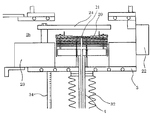
- FIG. 1 is a schematic view schematically showing the overall configuration of an electron impact heating apparatus.
- the electron impact heating apparatus 1 used in the present invention applies an acceleration voltage from an acceleration power source 42 to the thermoelectrons generated from the filament 14, collides the accelerated thermoelectrons with the heating container 11 to heat the heating container 11, and releases the heat.
- This is an apparatus for performing a heat treatment of the processing substrate 21 arranged to face the surface 11a.
- the electron impact heating apparatus 1 includes a vacuum chamber 3 that can be evacuated to form a compartment by connecting a processing chamber 2a for heat-treating a processing substrate 21 and a standby chamber 2b in the vertical direction.
- a heating device (hereinafter referred to as “heater”) 10 in which a filament 14 is incorporated is provided inside the upper processing chamber 2a.
- the heater 10 includes a cylindrical heating container 11 whose one end is closed, a filament base 12, a support column 13 and a filament 14 housed therein.
- the filament 14 is, for example, a closed end face of the heating container 11 (of the heater 10) by a tantalum support 13 having a diameter of ⁇ 2 mm that stands on a filament base 12 made of a carbon fiber reinforced composite material (hereinafter referred to as “CC composite”).
- CC composite carbon fiber reinforced composite material
- the filament 14 for example, a tungsten / rhenium wire or a tungsten wire to which a rare earth such as potassium or lanthanum is added is used, and one having a diameter of ⁇ 0.8 mm and a length of 900 mm is used.
- the heating container 11 is formed of a conductor. Specifically, the outer surface of the heating container 11 is coated with, for example, pyrolytic carbon so that the amount of released gas is reduced.
- the heating vessel 11 is connected to a vacuum evacuation unit (not shown), and the inside can be evacuated independently of the vacuum vessel 3.
- a CC composite substrate stage 20 is disposed so as to face the closed end surface (heat radiating surface of the heater 10) 11a of the heating container 11.
- a processing substrate (wafer) 21 is placed facing the heater 10.
- a silicon carbide (SiC) substrate is employed as the processing substrate 21, but is not limited thereto.
- the substrate stage 20 is supported by a cylindrical column 4, and a two-color radiation thermometer 7 is connected to the tip of the through hole 5 of the column 4 via a quartz viewing port 6. .
- the viewing port 6 closes the vacuum space to define a vacuum state and an atmospheric state. Radiation light from the substrate stage 20 or the processing substrate 21 reaches the two-color radiation thermometer 7 through this viewing port 6.
- the two-color radiation thermometer 7 includes, for example, a condensing unit 8 and a detector 9, and indirectly measures the temperature of the heater 10 via a substrate stage 20 made of CC composite.
- the temperature measurement is not limited to the temperature measurement of the substrate stage 20, and the temperature of the heat radiating surface 11 a of the heater 10 or the side surface of the heater 10 may be measured.
- a support plate 31 is fixed to the lower end of the support column 4, and a bellows 32 is interposed between the support plate 31 and the vacuum vessel 3. Further, an elevating arm 33 having a screw hole (not shown) is fixed to the support plate 31, and a ball screw 34 connected to the rotation drive device 35 is inserted into the screw hole of the elevating arm 33. That is, by rotating the ball screw 34 by the rotation drive device 35, the lifting arm 33 moves up and down along the ball screw 34, and the substrate stage 20 connected to the lifting arm 33 via the support column 4 can be moved up and down. It has become.
- the inside of the vacuum vessel 3 is evacuated by an exhaust device (not shown) connected to the exhaust port 25.
- a slit valve 22 is provided on one side wall of the standby chamber 2b of the vacuum vessel 3.
- the processing substrate 21 is carried into the vacuum vessel 3 by a transfer robot (not shown).
- the vacuum vessel 3 is carried out.
- a water-cooled shutter 24 connected to a rotation device 23 is provided in the standby chamber 2b of the vacuum vessel 3 so as to be rotatable in the horizontal direction. The water-cooled shutter 24 enters between the substrate stage 20 and the heat radiating surface 11a of the heater 10 when the substrate stage 20 is retracted into the standby chamber 2b so as to block the processing substrate 21 from the heat radiating surface 11a. It has become.
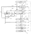
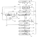
- FIG. 3 is a schematic diagram showing the configuration of the control system of the electron impact heating apparatus.
- the control system 40 of this embodiment includes an acceleration power source, a filament power source, an acceleration voltmeter, a filament ammeter, an emission ammeter, a heating power source including a thyristor, a multi-function temperature controller, a sequencer, and a pyrometer.
- a condensing part and a pyrometer main body are provided.
- the filament power supply 41 is an AC power supply that supplies power for heating the filament 14 and can be variably applied, for example, up to 50 A (ampere).
- a filament ammeter 45 is connected to the connection circuit of the filament 14 and the current value of the filament 14 is measured.
- the accelerating power source (HV power source) 42 is a DC power source that applies an accelerating voltage between the grounded heating vessel 11 and the filament 14, and is variable from 0 V (volt) to ⁇ 3.0 KV with respect to the filament 14, for example. Thus, an acceleration voltage can be applied.
- An acceleration voltmeter (HV voltmeter) 46 that measures an acceleration voltage and an emission ammeter 47 that measures an emission current value are connected to the connection circuit of the acceleration power source 42.
- the multi-function temperature controller 43 for example, SDC-46A manufactured by Yamatake Corporation is adopted.
- the multi-function temperature controller 43 receives an input signal from the filament ammeter 45, an input signal from the emission ammeter 47, and an input signal from the acceleration voltmeter 46, and also receives a set value from the sequencer 49. .
- the set value of the sequencer 49 is also input to the thyristor 48.
- the multi-function temperature controller 43 transmits an output signal to the filament power supply 41 via the thyristor 48.
- FIG. 2 is a schematic view showing a state where the substrate stage of the electron impact heating apparatus of FIG. 1 is lowered.
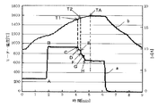
- FIG. 4 is an explanatory diagram showing the relationship between the temperature of the substrate stage and the emission current value in the temperature control method according to the present invention.
- the algorithm of the temperature control method according to the present invention is stored as a temperature control program in the storage unit of the control device (PC), and is read out and executed by the CPU at the start of the heat treatment.
- the temperature control program is a program for causing the control device to control the temperature of the heater 10 based on a detection signal or the like of the back surface temperature of the substrate stage 20. That is, the temperature control program of this embodiment has a procedure for raising the processing temperature while maintaining the emission current value of the acceleration power supply 42 constant. Further, after the processing temperature reaches the set temperature before the annealing temperature is reached, the emission current value is decreased stepwise and the temperature rise is continued. Then, after the processing temperature reaches the annealing temperature, it has a procedure of keeping the emission current value constant at the time when the annealing temperature is reached until the annealing processing is completed. When the annealing time takes a long time, the emission current value may be further reduced stepwise from the time when the annealing temperature is reached.
- the temperature control program is recorded on a recording medium readable by a control device such as a computer (PC) and installed in a storage unit of the PC.
- a control device such as a computer (PC) and installed in a storage unit of the PC.
- Recording media include floppy (registered trademark) disk, ZIP (registered trademark) magnetic recording medium, MO magneto-optical recording medium, CD-R, DVD-R, DVD + R, CD-R, DVD-RAM, DVD + RW (Registered trademark), optical disks such as PD, and the like. Further, there are flash memory systems such as CompactFlash (registered trademark), SmartMedia (registered trademark), Memory Stick (registered trademark), SD card, and removable disks such as Microdrive (registered trademark) and Jaz (registered trademark).
- the slit valve 22 (see FIG. 1) of the electron impact heating apparatus 1 is opened, and the SiC substrate 21 is carried into the standby chamber 2b of the vacuum vessel 3 by a transfer robot (not shown).
- the substrate stage 20 is retracted into the standby chamber 2b, and the water-cooled shutter 24 enters between the substrate stage 20 and the heat radiation surface 11a of the heater 10 (see FIG. 2).
- the slit valve 22 is closed, and the vacuum vessel 3 is evacuated by an unillustrated exhaust device connected to the exhaust port 25.
- the water cooling shutter 24 is rotated by the rotating device 23 and moved backward, and the ball screw 34 is rotated by the rotation driving device 35 to raise the substrate stage 20.
- a curve a shows the relationship between the elapsed time from the emission current application and the emission current value.
- Curve b shows the relationship between the elapsed time from the emission current application and the substrate stage temperature.
- the emission current value is rapidly increased to B at time A. Thereafter, the processing temperature is raised while maintaining the emission current value constant.
- the emission current value is controlled by first comparing the input signal from the emission ammeter 47 with the set value from the sequencer 49 by the multi-function temperature controller 43.
- the multifunction temperature controller 43 inputs the signal value after comparison to the thyristor 48 and controls the filament current value by the input signal from the thyristor 48 to the filament power supply 41.
- the set temperature T1 is set to a temperature lower than the annealing temperature TA by a predetermined temperature. For example, when the annealing temperature TA is 1500 ° C. to 2000 ° C., the set temperature T1 is preferably set to a temperature that is 40 ° C. to 100 ° C. lower than the annealing temperature TA. Further, at time E when the temperature of the substrate stage 20 rises and reaches the next set temperature T2, the emission current value is further lowered to F. This set temperature T2 is preferably set to a temperature 20 to 30 ° C. higher than the set temperature T1.
- the emission current value is further lowered to H.
- An activation annealing process is performed for a predetermined time (for example, 1 minute) from the time point I when the annealing temperature TA is reached.
- the emission current value is reduced to almost zero.
- the annealing process may be started from the time F.
- the number of times the emission current value is lowered is determined by the emission current value that is kept constant between B and C in order to increase the temperature at high speed so as not to overshoot.
- the emission current value between B and C is low, it is considered possible to reduce the emission current value to two stages.
- the emission current value can be lowered in a number of steps to increase the temperature rapidly without overshoot.
- the heater 10 When the series of heat treatment such as activation annealing is completed, the heater 10 is turned off. Thereafter, the ball screw 34 is reversely rotated by the rotation drive device 35 to lower the substrate stage 20, and the water cooling shutter 24 is rotated by the rotation device 23 to enter between the substrate stage 20 and the heat radiation surface 11 a of the heater 10. (See FIG. 2). Then, the slit valve 22 of the electronic impact heating device 1 is opened, and the SiC substrate 21 is carried out of the vacuum vessel 3 by the transfer robot.
- the temperature control method of the present embodiment the temperature is increased while maintaining the emission current value of the acceleration power supply 42 constant (between BC). Then, after reaching the set temperature T1 before reaching the annealing temperature TA, the emission current value is decreased stepwise and the temperature rise is continued, so the temperature control response is better than the PID control. This is because the PID control is a kind of feedback control, and the control is performed after detecting the amount of change, so the responsiveness is poor.
- the temperature control method according to the present invention reduces the emission current value stepwise and continues to raise the temperature, so that it becomes a kind of predictive control and has excellent responsiveness.
- the annealing process by the temperature control method can be employed.
- the productivity of the semiconductor device using the large-diameter SiC substrate 21 can be greatly improved.
- the temperature can be controlled by measuring the back surface temperature of the substrate stage without directly measuring the heater temperature and applying feedback.
- PID control is used at the time of heat retention after the output of the heating source is reduced by only one stage, the temperature cannot be controlled with high speed and good stability. This is probably due to the following reasons. That is, as the substrate size increases, the heat capacity due to the expansion of the heater and the substrate stage increases.
- thermoelectrons are generated from the filament in order to use an ultrahigh temperature region of 1500 ° C. or higher. Therefore, in this temperature region, even if the filament current is varied, the change in the filament temperature is delayed.
- the present invention has been described above by taking the electron impact heating device as an example, but the present invention can also be used in a temperature control method using a dielectric heating device and a resistance heating device.
- the present invention is not limited to the above-described embodiment, and various modifications can be made within the technical scope grasped from the description of the scope of claims.
- the power value applied to the heating body dielectric coil
- the resistance heating device the power value applied to the heating body (heating resistor) is decreased stepwise.
- Example 1 describes a case where a semiconductor device is manufactured using the temperature control method of the present invention using the electron impact heating apparatus 1 of FIGS. 1 and 2.
- Example 1 activation annealing treatment was performed on the SiC substrate 21 having a diameter of 100 mm into which impurities were implanted.
- the back surface temperature (hereinafter referred to as “annealing temperature”) of the substrate stage 20 at the time of holding the annealing temperature in this example was 1575 ° C. and was heated for 1 minute.
- the slit valve 22 of the electron impact heating apparatus 1 is opened, and the SiC substrate 21 is transferred onto the substrate stage 20 in the standby chamber 2b by the transfer robot.
- the SiC substrate 21 is scooped on the substrate stage 20 and the substrate stage 20 is raised by rotating the ball screw 34 with the rotation driving device 35 so that the distance between the heat radiation surface of the heater 10 and the SiC substrate 21 is 5 mm.
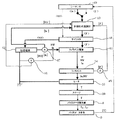
- FIGS. 5 to 8 are explanatory diagrams showing a sequence to which the temperature control method according to the present invention is applied.
- 5 shows a sequence at the time of heating the filament
- FIG. 6 shows a sequence at the time of increasing the acceleration voltage
- FIG. 7 shows a sequence at the time of emission current control
- FIG. 8 shows a sequence at the time of cooling.
- the filament 14 is heated to release the adsorbed gas to the filament 14 to prevent the filament 14 from deteriorating.
- a signal for increasing the filament current value by 1 A per second is input from the sequencer 49 to the multi-function temperature controller 43 so that the filament current value becomes 30 A.
- the multi-function temperature controller 43 compares the return signal from the filament ammeter 45 and outputs a signal to the thyristor 48.
- the filament power supply 41 gradually increases the output of the filament current value according to the input from the thyristor 48, and heats the filament 14 until the filament current value reaches 30A.
- an acceleration voltage (HV) is applied from the acceleration power source 42 to the filament 14 to gradually increase the voltage, thereby preventing a sudden increase in emission current value and preventing abnormal discharge.
- the sequencer 49 outputs a signal to the thyristor 48 so that the acceleration voltage (HV) ⁇ 500 V is applied while the filament current value is fixed at 30 A.
- an acceleration voltage (HV) ⁇ 500 V is applied to the filament 14 in accordance with an input from the thyristor 48.
- the sequencer 49 outputs to the thyristor 48 a signal for increasing the acceleration voltage (HV) by -100V per second so that the acceleration voltage (HV) becomes -1800V.
- the acceleration power source 42 gradually increases the output of the acceleration voltage (HV) in accordance with the input of the thyristor 48 so that the acceleration voltage (HV) becomes ⁇ 1800 V and generates an emission current.
- the adsorption gas such as moisture brought into the vacuum vessel 3 by the SiC substrate 21 is preheated and removed.
- a signal indicating an emission current value of 3 A is input from the sequencer 49 to the multi-function temperature controller 43.
- the filament current value is controlled from the multi-function temperature controller 43 so that the acceleration current (HV) remains constant at ⁇ 1800 V and is compared with the output signal from the emission ammeter so that the emission current value becomes 3A.
- a signal for performing this operation is input to the thyristor 48.
- the filament power supply 41 controls the emission current value to be 3A.
- an outgas treatment is performed by preheating for 90 seconds at an emission current value of 3A.
- the back surface temperature of the substrate stage 20 at the end of the preheating is 1200 ° C. This preheating step can be omitted depending on the sample.
- the sequencer 49 inputs a signal to the multi-function temperature controller 43 so that the emission current value becomes 10.2A.
- the accelerating voltage (HV) remains constant at -1800 V, and compared with the output signal from the emission ammeter, the filament temperature value from the multi-function temperature controller 43 is adjusted so that the emission current value becomes 10.2 A.
- a signal for controlling is input to the thyristor 48.
- the filament power supply 41 controls the filament current value so that the emission current value becomes 10.2 A by the input signal from the thyristor 48, thereby rapidly heating the heater and heating the SiC substrate 21 (initial temperature rise). ).
- the filament power supply 41 compares the value of the emission ammeter with the input signal through the sequencer 49, the multi-function temperature controller 43 and the thyristor 48. To do. Further, the filament power supply 41 controls the filament current value so that the emission current value becomes 9.5 A and raises the temperature to 1535 ° C. (temperature range I). The acceleration voltage (HV) at this time is kept constant at ⁇ 1800V. Then, by reducing the emission current value from 10.2 A to 9.5 A at 60 ° C. just before the set annealing temperature of 1575 ° C., it is possible to moderately control the temperature rise and prevent temperature overshoot and undershoot.
- HV acceleration voltage
- the filament power supply 41 compares the value of the emission ammeter with the input signal through the sequencer 49, the multi-function temperature controller 43 and the thyristor 48. To do. Further, the filament power supply 41 controls the filament current value so that the emission current value becomes 8.4 A and raises the temperature to 1555 ° C. (temperature range II).
- the acceleration voltage (HV) at this time is kept constant at ⁇ 1800V.
- the filament power supply 41 compares the value of the emission ammeter with the input signal through the sequencer 49, the multi-function temperature controller 43, and the thyristor 48. To do. Further, the filament power supply 41 controls the filament current value so that the emission current value becomes 7.3 A and raises the temperature to 1575 ° C. (temperature range III).
- the acceleration voltage (HV) at this time is kept constant at ⁇ 1800V.
- the filament power supply 41 is compared with the value of the emission ammeter by the input signal through the sequencer 49, the multi-function temperature controller 43 and the thyristor 48. To do. Furthermore, the filament power supply 41 controls the filament current value so that the emission current value becomes 7.1 A, and performs the annealing process for 1 minute.
- the acceleration voltage (HV) at this time is kept constant at ⁇ 1800V.
- the slit valve 22 of the electronic impact heating apparatus 1 is opened, and the SiC substrate 21 is carried out of the vacuum vessel 3 by the transfer robot.
- the processing time per substrate was 9 minutes and 24 seconds, and the temperature stability was + 1 ° C. and ⁇ 5 ° C. Furthermore, when 10 sheets of SiC substrate 21 were set in a cassette and a series of processes of evacuation, transfer, heat treatment, transfer and vent were performed, the processing time was 1 hour and 47 minutes, and the throughput was 5 sheets / hour. The above has been achieved.
- the annealing time is as short as 1 minute.
- the annealing time may be as long as 5 to 10 minutes depending on the type of sample annealing.
- the emission current value is increased or decreased with time after the set annealing temperature is reached. For example, when annealing at a substrate stage temperature of 1575 ° C. for 10 minutes, after annealing for 3 minutes at 7.1 A, anneal for 3 minutes at 7.0 A for 3 to 6 minutes, and then for 6.9 A for 6 to 10 minutes. Can also be annealed for 4 minutes.
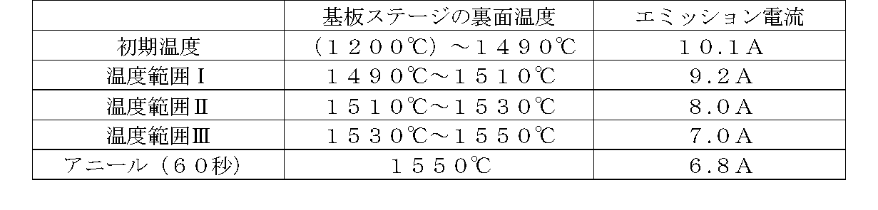
- Example 2 In the second embodiment, the case where the activation annealing process is performed at 1500 ° C. for one minute using the same substrate as in the first embodiment will be described.
- Example 1 the temperature was raised at 3A for 90 seconds for degassing, and after the back surface temperature of the substrate stage 20 reached 1200 ° C., the initial temperature rise in steps (4) to (8), temperature ranges I and II. , III and the set temperature and the emission current value in the annealing treatment were changed to the values shown in Table 1. Except this, the substrate was processed in the same manner as in Example 1.
- Example 3 In Example 3, a case will be described in which activation annealing is performed at 1550 ° C. for 1 minute using the same substrate as in Example 1.
- Example 1 the temperature was raised at 3A for 90 seconds for degassing, and after the back surface temperature of the substrate stage 20 reached 1200 ° C., the initial temperature rise in steps (4) to (8), temperature ranges I and II. , III and the set temperature and the emission current value in the annealing treatment were changed to the values shown in Table 2. Except this, the substrate was processed in the same manner as in Example 1.
- Example 4 In the fourth embodiment, the case where the same annealing substrate as that of the first embodiment is used and the activation annealing process is performed at 1600 ° C. for 1 minute will be described.
- Example 1 the temperature was raised at 3A for 90 seconds for degassing, and after the back surface temperature of the substrate stage 20 reached 1200 ° C., the initial temperature rise in steps (4) to (8), temperature ranges I and II. , III and the set temperature and the emission current value in the annealing treatment were changed to the values shown in Table 3. Except this, the substrate was processed in the same manner as in Example 1.
- Example 2 to Example 4 good results were obtained as in Example 1. That is, according to the present invention, by suppressing the hunting of the annealing temperature and rapidly heating the ultra-high temperature, the impurities implanted into the SiC substrate 21 can be activated with high reproducibility and high throughput. Accordingly, it has been found that the manufacturing cost in the method for manufacturing the silicon carbide (SiC) semiconductor device can be greatly improved.
- Substrate heat treatment device Electric impact heating device 2a Processing chamber 3 Vacuum vessel 10 Heating device 11 Heating vessel 14 Filament 21 Processing substrate 42 Acceleration power supply 46 Acceleration voltmeter 47 Emission ammeter
Landscapes
- Control Of Resistance Heating (AREA)
Abstract
Description
即ち、本発明に係る基板加熱処理装置の温度制御方法は、真空排気可能な処理室の内部に、加熱体を備え、前記加熱体により基板の熱処理を行う基板加熱処理装置の温度制御方法であって、
処理温度を上昇させる手順と、
前記処理温度がアニール温度に到達前の設定温度に到達した後、前記加熱体を加熱するために印加する電力値を段階的に低下させて昇温を継続する手順と、
前記処理温度がアニール温度に到達した後アニール処理が完了するまで、処理温度を一定に維持する手順と、
を有することを特徴とする基板加熱処理装置の温度制御方法である。
前記フィラメントと前記加熱容器との間に、加速電源により印加された加速電圧で、前記フィラメントから発生する熱電子を加速し、該加速した熱電子を前記加熱容器に衝突させて該加熱容器を加熱し、該加熱容器の熱により基板の熱処理を行う基板加熱処理装置の温度制御方法であって、
処理温度を上昇させる手順と、
前記処理温度がアニール温度に到達前の設定温度に到達した後、前記加速電源のエミッション電流値を段階的に低下させて昇温を継続する手順と、
前記処理温度がアニール温度に到達した後アニール処理が完了するまで、処理温度を一定に維持する手順と、
を有することを特徴とする基板加熱処理装置の温度制御方法である。
また、ヒータ温度を直接測定してフィードバックをかけなくても、基板ステージの裏面温度を測定することで、温度制御が可能となる。
一方、加熱源の出力を一段階のみ低下させた後の保温時にPID制御を用いる場合には、高速、安定性良く温度を制御することが出来ない。これは、以下の理由によるものと思われる。すなわち、基板サイズの大口径化に伴い、ヒータや基板ステージの拡大による熱容量が増大している。また、SiC基板の活性化アニール処理には、1500℃以上の超高温領域を用いるためにフィラメントから熱電子を発生させている。そのため、この温度領域では、フィラメント電流を可変させても、フィラメント温度の変化が遅くなる。
実施例1は、図1及び図2の電子衝撃加熱装置1を用いて、本発明の温度制御方法を用いて半導体デバイスを製造する場合について説明する。
実施例2では、実施例1と同じ基板を用いて、1500℃で1分間の活性化アニール処理を施す場合について説明する。

実施例3では、実施例1と同じ基板を用いて、1550℃で1分間の活性化アニール処理を施す場合について説明する。
実施例4では、実施例1と同じ基板を用いて、1600℃で1分間の活性化アニール処理を施す場合について説明する。

2a 処理室
3 真空容器
10 加熱装置
11 加熱容器
14 フィラメント
21 処理基板
42 加速電源
46 加速電圧計
47 エミッション電流計
Claims (13)
- 真空排気可能な処理室の内部に、加熱体を備え、前記加熱体により基板の熱処理を行う基板加熱処理装置の温度制御方法であって、
処理温度を上昇させる手順と、
前記処理温度がアニール温度に到達前の設定温度に到達した後、前記加熱体を加熱するために印加する電力値を段階的に低下させて昇温を継続する手順と、
前記処理温度がアニール温度に到達した後アニール処理が完了するまで、処理温度を一定に維持する手順と、
を有することを特徴とする基板加熱処理装置の温度制御方法。 - 真空排気可能な処理室の内部に、フィラメントを組み込んだ導電体の加熱容器を備え、
前記フィラメントと前記加熱容器との間に、加速電源により印加された加速電圧で、前記フィラメントから発生する熱電子を加速し、該加速した熱電子を前記加熱容器に衝突させて該加熱容器を加熱し、該加熱容器の熱により基板の熱処理を行う基板加熱処理装置の温度制御方法であって、
処理温度を上昇させる手順と、
前記処理温度がアニール温度に到達前の設定温度に到達した後、前記加速電源のエミッション電流値を段階的に低下させて昇温を継続する手順と、
前記処理温度がアニール温度に到達した後アニール処理が完了するまで、処理温度を一定に維持する手順と、
を有することを特徴とする基板加熱処理装置の温度制御方法。 - 前記処理室内に、基板を載置する基板ステージを具備することを特徴とする請求項2に記載の温度制御方法。
- 前記処理温度を上昇させる手順が、前記加速電源のエミッション電流値を一定に維持して処理温度を上昇させる手順であることを特徴とする請求項2または3に記載の基板加熱処理装置の温度制御方法。
- 前記処理温度を一定に維持する手順が、アニール温度に到達時点の前記加速電源のエミッション電流値で前記処理温度を一定に維持する手順であることを特徴とする請求項2から4のいずれか1項に記載の基板加熱処理装置の温度制御方法。
- 前記アニール温度が1500℃~2000℃の場合に、前記設定温度をアニール温度よりも40℃~100℃低い温度に設定することを特徴とする請求項2から5のいずれか1項に記載の基板加熱処理装置の温度制御方法。
- 前記処理温度は、前記基板ステージの裏面温度として検出することを特徴とする請求項3から6のいずれか1項に記載の基板加熱処理装置の温度制御方法。
- 炭化珪素基板に不純物をイオン注入した後、アニール処理して不純物を活性化させるアニール処理の工程を有する半導体デバイスの製造方法において、
請求項1から7のいずれか1項に記載の方法により温度制御して前記アニール処理を行うことを特徴とする半導体デバイスの製造方法。 - 真空排気可能な処理室の内部に、フィラメントを組み込んだ導電体の加熱容器を備え、
前記フィラメントと前記加熱容器との間に、加速電源により印加された加速電圧で、前記フィラメントから発生する熱電子を加速し、該加速した熱電子を前記加熱容器に衝突させて該加熱容器を加熱し、該加熱容器の熱により基板の熱処理を行う基板加熱処理装置の温度制御プログラムであって、
処理温度を上昇させる手順と、
前記処理温度がアニール温度に到達前の設定温度に到達した後、前記加速電源のエミッション電流値を段階的に低下させて昇温を継続する手順と、
前記処理温度がアニール温度に到達した後アニール処理が完了するまで、処理温度を一定に維持する手順と、
を前記基板加熱処理装置の制御装置に実行させることを特徴とする基板加熱処理装置の温度制御プログラム。 - 前記処理温度を上昇させる手順が、前記加速電源のエミッション電流値を一定に維持して処理温度を上昇させる手順であることを特徴とする請求項9に記載の基板加熱処理装置の温度制御プログラム。
- 前記処理温度を一定に維持する手順が、アニール温度に到達時点の前記加速電源のエミッション電流値で前記処理温度を一定に維持する手順であることを特徴とする請求項9または10に記載の基板加熱処理装置の温度制御プログラム。
- 前記アニール温度が1500℃~2000℃の場合に、前記設定温度をアニール温度よりも40℃~100℃低い温度に設定することを特徴とする請求項9から11のいずれか1項に記載の基板加熱処理装置の温度制御プログラム。
- 請求項9から12のいずれか1項に記載の温度制御プログラムを記録したコンピュータで読み取り可能な記録媒体。
Priority Applications (2)
| Application Number | Priority Date | Filing Date | Title |
|---|---|---|---|
| JP2011547298A JP5469678B2 (ja) | 2009-12-25 | 2010-12-21 | 基板加熱処理装置の温度制御方法、半導体デバイスの製造方法、基板加熱処理装置の温度制御プログラム及び記録媒体 |
| US13/511,092 US9431281B2 (en) | 2009-12-25 | 2010-12-21 | Temperature control method for substrate heat treatment apparatus, semiconductor device manufacturing method, temperature control program for substrate heat treatment apparatus, and recording medium |
Applications Claiming Priority (2)
| Application Number | Priority Date | Filing Date | Title |
|---|---|---|---|
| JP2009295665 | 2009-12-25 | ||
| JP2009-295665 | 2009-12-25 |
Publications (1)
| Publication Number | Publication Date |
|---|---|
| WO2011077702A1 true WO2011077702A1 (ja) | 2011-06-30 |
Family
ID=44195256
Family Applications (1)
| Application Number | Title | Priority Date | Filing Date |
|---|---|---|---|
| PCT/JP2010/007397 Ceased WO2011077702A1 (ja) | 2009-12-25 | 2010-12-21 | 基板加熱処理装置の温度制御方法、半導体デバイスの製造方法、基板加熱処理装置の温度制御プログラム及び記録媒体 |
Country Status (3)
| Country | Link |
|---|---|
| US (1) | US9431281B2 (ja) |
| JP (1) | JP5469678B2 (ja) |
| WO (1) | WO2011077702A1 (ja) |
Cited By (2)
| Publication number | Priority date | Publication date | Assignee | Title |
|---|---|---|---|---|
| JP5543601B2 (ja) * | 2010-08-09 | 2014-07-09 | キヤノンアネルバ株式会社 | 基板加熱処理装置、基板加熱処理装置の温度制御方法、半導体デバイスの製造方法、基板加熱処理装置の温度制御プログラム及び記録媒体 |
| JP2019212683A (ja) * | 2018-05-31 | 2019-12-12 | 三菱電機株式会社 | 半導体装置の製造方法 |
Families Citing this family (4)
| Publication number | Priority date | Publication date | Assignee | Title |
|---|---|---|---|---|
| WO2014149962A1 (en) * | 2013-03-14 | 2014-09-25 | Applied Materials, Inc. | Apparatus for coupling a hot wire source to a process chamber |
| WO2015146162A1 (ja) | 2014-03-24 | 2015-10-01 | キヤノンアネルバ株式会社 | 半導体基板の熱処理方法及び熱処理装置 |
| US20180053666A1 (en) * | 2016-08-19 | 2018-02-22 | Applied Materials, Inc. | Substrate carrier with array of independently controllable heater elements |
| CN112684832B (zh) * | 2019-10-17 | 2022-01-28 | 中国石油化工股份有限公司 | 克服碳化硅环状载体温度反应滞后的方法及设备 |
Citations (8)
| Publication number | Priority date | Publication date | Assignee | Title |
|---|---|---|---|---|
| JPS62160512A (ja) * | 1986-01-08 | 1987-07-16 | Dainippon Screen Mfg Co Ltd | 半導体基板の熱処理装置における温度制御方法および温度制御装置 |
| JPH07312351A (ja) * | 1994-05-17 | 1995-11-28 | Tokyo Electron Ltd | 熱処理方法 |
| JP2001345275A (ja) * | 2000-06-01 | 2001-12-14 | Tokyo Electron Ltd | 熱処理装置、熱処理装置の制御方法、および基板の周縁測定箇所の決定方法 |
| JP2005056964A (ja) * | 2003-08-01 | 2005-03-03 | Sukegawa Electric Co Ltd | 電子衝撃加熱装置 |
| JP2005056582A (ja) * | 2003-05-09 | 2005-03-03 | Sukegawa Electric Co Ltd | 電子衝撃加熱器の温度制御装置と温度制御方法 |
| JP2006230146A (ja) * | 2005-02-18 | 2006-08-31 | Tokyo Electron Ltd | 複数の電力使用系の動作制御装置、動作制御方法及び記憶媒体 |
| JP2008288480A (ja) * | 2007-05-21 | 2008-11-27 | Renesas Technology Corp | 半導体装置の製造方法 |
| JP2009200401A (ja) * | 2008-02-25 | 2009-09-03 | Ushio Inc | 光照射式加熱方法及び光照射式加熱装置 |
Family Cites Families (12)
| Publication number | Priority date | Publication date | Assignee | Title |
|---|---|---|---|---|
| JPS61145606A (ja) * | 1984-12-19 | 1986-07-03 | Ohkura Electric Co Ltd | 干渉対応形パタ−ン切換式温度制御装置 |
| KR910002596B1 (ko) | 1985-11-21 | 1991-04-27 | 다이닛뽕 스크린 세이조오 가부시기가이샤 | 온도제어방법 및 그 장치 |
| US5775889A (en) | 1994-05-17 | 1998-07-07 | Tokyo Electron Limited | Heat treatment process for preventing slips in semiconductor wafers |
| KR100486158B1 (ko) * | 1996-01-31 | 2005-11-08 | 에이에스엠 아메리카, 인코포레이티드 | 열처리의모델베이스예측제어 |
| JP2001044184A (ja) | 1999-07-27 | 2001-02-16 | Sony Corp | 半導体基板加熱装置 |
| US7320733B2 (en) | 2003-05-09 | 2008-01-22 | Sukegawa Electric Co., Ltd. | Electron bombardment heating apparatus and temperature controlling apparatus and control method thereof |
| JP4811860B2 (ja) * | 2006-05-10 | 2011-11-09 | 東京エレクトロン株式会社 | 熱処理方法、そのプログラム及び熱処理装置 |
| WO2008142747A1 (ja) | 2007-05-16 | 2008-11-27 | Canon Anelva Corporation | 加熱処理装置 |
| JP4288309B2 (ja) | 2007-09-03 | 2009-07-01 | キヤノンアネルバ株式会社 | 基板熱処理装置及び基板の熱処理方法 |
| JP4617364B2 (ja) * | 2008-02-29 | 2011-01-26 | キヤノンアネルバ株式会社 | 基板加熱装置及び処理方法 |
| JP2010251718A (ja) | 2009-03-27 | 2010-11-04 | Canon Anelva Corp | 加熱装置の温度制御方法及び記憶媒体 |
| JP2010096768A (ja) | 2009-12-28 | 2010-04-30 | Canon Anelva Corp | 加熱処理装置 |
-
2010
- 2010-12-21 US US13/511,092 patent/US9431281B2/en active Active
- 2010-12-21 WO PCT/JP2010/007397 patent/WO2011077702A1/ja not_active Ceased
- 2010-12-21 JP JP2011547298A patent/JP5469678B2/ja not_active Expired - Fee Related
Patent Citations (8)
| Publication number | Priority date | Publication date | Assignee | Title |
|---|---|---|---|---|
| JPS62160512A (ja) * | 1986-01-08 | 1987-07-16 | Dainippon Screen Mfg Co Ltd | 半導体基板の熱処理装置における温度制御方法および温度制御装置 |
| JPH07312351A (ja) * | 1994-05-17 | 1995-11-28 | Tokyo Electron Ltd | 熱処理方法 |
| JP2001345275A (ja) * | 2000-06-01 | 2001-12-14 | Tokyo Electron Ltd | 熱処理装置、熱処理装置の制御方法、および基板の周縁測定箇所の決定方法 |
| JP2005056582A (ja) * | 2003-05-09 | 2005-03-03 | Sukegawa Electric Co Ltd | 電子衝撃加熱器の温度制御装置と温度制御方法 |
| JP2005056964A (ja) * | 2003-08-01 | 2005-03-03 | Sukegawa Electric Co Ltd | 電子衝撃加熱装置 |
| JP2006230146A (ja) * | 2005-02-18 | 2006-08-31 | Tokyo Electron Ltd | 複数の電力使用系の動作制御装置、動作制御方法及び記憶媒体 |
| JP2008288480A (ja) * | 2007-05-21 | 2008-11-27 | Renesas Technology Corp | 半導体装置の製造方法 |
| JP2009200401A (ja) * | 2008-02-25 | 2009-09-03 | Ushio Inc | 光照射式加熱方法及び光照射式加熱装置 |
Cited By (2)
| Publication number | Priority date | Publication date | Assignee | Title |
|---|---|---|---|---|
| JP5543601B2 (ja) * | 2010-08-09 | 2014-07-09 | キヤノンアネルバ株式会社 | 基板加熱処理装置、基板加熱処理装置の温度制御方法、半導体デバイスの製造方法、基板加熱処理装置の温度制御プログラム及び記録媒体 |
| JP2019212683A (ja) * | 2018-05-31 | 2019-12-12 | 三菱電機株式会社 | 半導体装置の製造方法 |
Also Published As
| Publication number | Publication date |
|---|---|
| US9431281B2 (en) | 2016-08-30 |
| JP5469678B2 (ja) | 2014-04-16 |
| US20120219921A1 (en) | 2012-08-30 |
| JPWO2011077702A1 (ja) | 2013-05-02 |
Similar Documents
| Publication | Publication Date | Title |
|---|---|---|
| US7655933B2 (en) | Techniques for temperature-controlled ion implantation | |
| US8450193B2 (en) | Techniques for temperature-controlled ion implantation | |
| US8837924B2 (en) | Vacuum heating/cooling apparatus and manufacturing method of magnetoresistance element | |
| JP5469678B2 (ja) | 基板加熱処理装置の温度制御方法、半導体デバイスの製造方法、基板加熱処理装置の温度制御プログラム及び記録媒体 | |
| JP5380525B2 (ja) | 真空加熱冷却装置 | |
| US10204809B2 (en) | Method for thermal treatment using heat reservoir chamber | |
| JP5543601B2 (ja) | 基板加熱処理装置、基板加熱処理装置の温度制御方法、半導体デバイスの製造方法、基板加熱処理装置の温度制御プログラム及び記録媒体 | |
| CN109417010B (zh) | 加热或冷却晶片的设备及方法 | |
| CN110199382A (zh) | 用于离子注入系统的主动工件加热或冷却 | |
| US20110073589A1 (en) | Thermal processing apparatus | |
| JP6005966B2 (ja) | 熱処理装置および熱処理方法 | |
| CN101847573B (zh) | 用于加热设备的温度控制方法 | |
| US20160057812A1 (en) | Vacuum processing device | |
| US7897523B2 (en) | Substrate heating apparatus, heating method, and semiconductor device manufacturing method | |
| JP2010073787A (ja) | 熱処理装置 | |
| JP2010258359A (ja) | 熱処理方法および熱処理装置 | |
| JP5483710B2 (ja) | 印加電圧設定方法、熱処理方法および熱処理装置 | |
| JP5770880B2 (ja) | 熱処理方法 | |
| JPH05160112A (ja) | プラズマ処理装置及びプラズマ処理方法 | |
| CN117187787A (zh) | 薄膜沉积设备及其控制方法以及存储介质 | |
| JP2014146831A (ja) | 熱処理方法 |
Legal Events
| Date | Code | Title | Description |
|---|---|---|---|
| 121 | Ep: the epo has been informed by wipo that ep was designated in this application |
Ref document number: 10838941 Country of ref document: EP Kind code of ref document: A1 |
|
| WWE | Wipo information: entry into national phase |
Ref document number: 13511092 Country of ref document: US |
|
| WWE | Wipo information: entry into national phase |
Ref document number: 2011547298 Country of ref document: JP |
|
| NENP | Non-entry into the national phase |
Ref country code: DE |
|
| 122 | Ep: pct application non-entry in european phase |
Ref document number: 10838941 Country of ref document: EP Kind code of ref document: A1 |