WO2011074234A1 - Solid-state image pickup apparatus - Google Patents
Solid-state image pickup apparatus Download PDFInfo
- Publication number
- WO2011074234A1 WO2011074234A1 PCT/JP2010/007224 JP2010007224W WO2011074234A1 WO 2011074234 A1 WO2011074234 A1 WO 2011074234A1 JP 2010007224 W JP2010007224 W JP 2010007224W WO 2011074234 A1 WO2011074234 A1 WO 2011074234A1
- Authority
- WO
- WIPO (PCT)
- Prior art keywords
- light
- semiconductor region
- type semiconductor
- image pickup
- disposed
- Prior art date
Links
- 239000004065 semiconductor Substances 0.000 claims abstract description 276
- 239000000969 carrier Substances 0.000 claims abstract description 60
- 239000000758 substrate Substances 0.000 claims abstract description 39
- 238000006243 chemical reaction Methods 0.000 claims abstract description 12
- 230000006870 function Effects 0.000 claims description 20
- 230000003287 optical effect Effects 0.000 claims description 17
- 230000009467 reduction Effects 0.000 claims description 14
- 238000012545 processing Methods 0.000 claims description 5
- 238000000034 method Methods 0.000 claims description 3
- 230000008569 process Effects 0.000 claims description 2
- 238000000926 separation method Methods 0.000 abstract description 22
- 238000005036 potential barrier Methods 0.000 description 13
- 238000009826 distribution Methods 0.000 description 11
- 230000007423 decrease Effects 0.000 description 9
- 239000012535 impurity Substances 0.000 description 9
- 230000008901 benefit Effects 0.000 description 7
- 239000010410 layer Substances 0.000 description 6
- 238000010586 diagram Methods 0.000 description 5
- 239000000463 material Substances 0.000 description 5
- 238000009792 diffusion process Methods 0.000 description 4
- 238000012546 transfer Methods 0.000 description 3
- IJGRMHOSHXDMSA-UHFFFAOYSA-N Atomic nitrogen Chemical compound N#N IJGRMHOSHXDMSA-UHFFFAOYSA-N 0.000 description 2
- 229910052751 metal Inorganic materials 0.000 description 2
- 239000002184 metal Substances 0.000 description 2
- 239000011358 absorbing material Substances 0.000 description 1
- 238000010521 absorption reaction Methods 0.000 description 1
- 229910052782 aluminium Inorganic materials 0.000 description 1
- XAGFODPZIPBFFR-UHFFFAOYSA-N aluminium Chemical compound [Al] XAGFODPZIPBFFR-UHFFFAOYSA-N 0.000 description 1
- 230000004888 barrier function Effects 0.000 description 1
- RKTYLMNFRDHKIL-UHFFFAOYSA-N copper;5,10,15,20-tetraphenylporphyrin-22,24-diide Chemical compound [Cu+2].C1=CC(C(=C2C=CC([N-]2)=C(C=2C=CC=CC=2)C=2C=CC(N=2)=C(C=2C=CC=CC=2)C2=CC=C3[N-]2)C=2C=CC=CC=2)=NC1=C3C1=CC=CC=C1 RKTYLMNFRDHKIL-UHFFFAOYSA-N 0.000 description 1
- 238000012937 correction Methods 0.000 description 1
- 230000001419 dependent effect Effects 0.000 description 1
- 239000011159 matrix material Substances 0.000 description 1
- 238000012986 modification Methods 0.000 description 1
- 230000004048 modification Effects 0.000 description 1
- 229910052757 nitrogen Inorganic materials 0.000 description 1
- 230000002093 peripheral effect Effects 0.000 description 1
- 239000011241 protective layer Substances 0.000 description 1
- 239000011347 resin Substances 0.000 description 1
- 229920005989 resin Polymers 0.000 description 1
- 230000007480 spreading Effects 0.000 description 1
Images
Classifications
-
- H—ELECTRICITY
- H01—ELECTRIC ELEMENTS
- H01L—SEMICONDUCTOR DEVICES NOT COVERED BY CLASS H10
- H01L27/00—Devices consisting of a plurality of semiconductor or other solid-state components formed in or on a common substrate
- H01L27/14—Devices consisting of a plurality of semiconductor or other solid-state components formed in or on a common substrate including semiconductor components sensitive to infrared radiation, light, electromagnetic radiation of shorter wavelength or corpuscular radiation and specially adapted either for the conversion of the energy of such radiation into electrical energy or for the control of electrical energy by such radiation
- H01L27/144—Devices controlled by radiation
- H01L27/146—Imager structures
- H01L27/14601—Structural or functional details thereof
- H01L27/14609—Pixel-elements with integrated switching, control, storage or amplification elements
- H01L27/1461—Pixel-elements with integrated switching, control, storage or amplification elements characterised by the photosensitive area
-
- H—ELECTRICITY
- H01—ELECTRIC ELEMENTS
- H01L—SEMICONDUCTOR DEVICES NOT COVERED BY CLASS H10
- H01L27/00—Devices consisting of a plurality of semiconductor or other solid-state components formed in or on a common substrate
- H01L27/14—Devices consisting of a plurality of semiconductor or other solid-state components formed in or on a common substrate including semiconductor components sensitive to infrared radiation, light, electromagnetic radiation of shorter wavelength or corpuscular radiation and specially adapted either for the conversion of the energy of such radiation into electrical energy or for the control of electrical energy by such radiation
- H01L27/144—Devices controlled by radiation
- H01L27/146—Imager structures
- H01L27/14601—Structural or functional details thereof
- H01L27/14603—Special geometry or disposition of pixel-elements, address-lines or gate-electrodes
- H01L27/14605—Structural or functional details relating to the position of the pixel elements, e.g. smaller pixel elements in the center of the imager compared to pixel elements at the periphery
-
- H—ELECTRICITY
- H01—ELECTRIC ELEMENTS
- H01L—SEMICONDUCTOR DEVICES NOT COVERED BY CLASS H10
- H01L27/00—Devices consisting of a plurality of semiconductor or other solid-state components formed in or on a common substrate
- H01L27/14—Devices consisting of a plurality of semiconductor or other solid-state components formed in or on a common substrate including semiconductor components sensitive to infrared radiation, light, electromagnetic radiation of shorter wavelength or corpuscular radiation and specially adapted either for the conversion of the energy of such radiation into electrical energy or for the control of electrical energy by such radiation
- H01L27/144—Devices controlled by radiation
- H01L27/146—Imager structures
- H01L27/14601—Structural or functional details thereof
- H01L27/1462—Coatings
- H01L27/14623—Optical shielding
-
- H—ELECTRICITY
- H01—ELECTRIC ELEMENTS
- H01L—SEMICONDUCTOR DEVICES NOT COVERED BY CLASS H10
- H01L27/00—Devices consisting of a plurality of semiconductor or other solid-state components formed in or on a common substrate
- H01L27/14—Devices consisting of a plurality of semiconductor or other solid-state components formed in or on a common substrate including semiconductor components sensitive to infrared radiation, light, electromagnetic radiation of shorter wavelength or corpuscular radiation and specially adapted either for the conversion of the energy of such radiation into electrical energy or for the control of electrical energy by such radiation
- H01L27/144—Devices controlled by radiation
- H01L27/146—Imager structures
- H01L27/14601—Structural or functional details thereof
- H01L27/14625—Optical elements or arrangements associated with the device
- H01L27/14627—Microlenses
-
- H—ELECTRICITY
- H01—ELECTRIC ELEMENTS
- H01L—SEMICONDUCTOR DEVICES NOT COVERED BY CLASS H10
- H01L27/00—Devices consisting of a plurality of semiconductor or other solid-state components formed in or on a common substrate
- H01L27/14—Devices consisting of a plurality of semiconductor or other solid-state components formed in or on a common substrate including semiconductor components sensitive to infrared radiation, light, electromagnetic radiation of shorter wavelength or corpuscular radiation and specially adapted either for the conversion of the energy of such radiation into electrical energy or for the control of electrical energy by such radiation
- H01L27/144—Devices controlled by radiation
- H01L27/146—Imager structures
- H01L27/14601—Structural or functional details thereof
- H01L27/14625—Optical elements or arrangements associated with the device
- H01L27/14629—Reflectors
-
- H—ELECTRICITY
- H01—ELECTRIC ELEMENTS
- H01L—SEMICONDUCTOR DEVICES NOT COVERED BY CLASS H10
- H01L27/00—Devices consisting of a plurality of semiconductor or other solid-state components formed in or on a common substrate
- H01L27/14—Devices consisting of a plurality of semiconductor or other solid-state components formed in or on a common substrate including semiconductor components sensitive to infrared radiation, light, electromagnetic radiation of shorter wavelength or corpuscular radiation and specially adapted either for the conversion of the energy of such radiation into electrical energy or for the control of electrical energy by such radiation
- H01L27/144—Devices controlled by radiation
- H01L27/146—Imager structures
- H01L27/14601—Structural or functional details thereof
- H01L27/14634—Assemblies, i.e. Hybrid structures
-
- H—ELECTRICITY
- H01—ELECTRIC ELEMENTS
- H01L—SEMICONDUCTOR DEVICES NOT COVERED BY CLASS H10
- H01L27/00—Devices consisting of a plurality of semiconductor or other solid-state components formed in or on a common substrate
- H01L27/14—Devices consisting of a plurality of semiconductor or other solid-state components formed in or on a common substrate including semiconductor components sensitive to infrared radiation, light, electromagnetic radiation of shorter wavelength or corpuscular radiation and specially adapted either for the conversion of the energy of such radiation into electrical energy or for the control of electrical energy by such radiation
- H01L27/144—Devices controlled by radiation
- H01L27/146—Imager structures
- H01L27/14601—Structural or functional details thereof
- H01L27/1464—Back illuminated imager structures
-
- H—ELECTRICITY
- H01—ELECTRIC ELEMENTS
- H01L—SEMICONDUCTOR DEVICES NOT COVERED BY CLASS H10
- H01L27/00—Devices consisting of a plurality of semiconductor or other solid-state components formed in or on a common substrate
- H01L27/14—Devices consisting of a plurality of semiconductor or other solid-state components formed in or on a common substrate including semiconductor components sensitive to infrared radiation, light, electromagnetic radiation of shorter wavelength or corpuscular radiation and specially adapted either for the conversion of the energy of such radiation into electrical energy or for the control of electrical energy by such radiation
- H01L27/144—Devices controlled by radiation
- H01L27/146—Imager structures
- H01L27/14643—Photodiode arrays; MOS imagers
- H01L27/14645—Colour imagers
- H01L27/14647—Multicolour imagers having a stacked pixel-element structure, e.g. npn, npnpn or MQW elements
-
- H—ELECTRICITY
- H01—ELECTRIC ELEMENTS
- H01L—SEMICONDUCTOR DEVICES NOT COVERED BY CLASS H10
- H01L27/00—Devices consisting of a plurality of semiconductor or other solid-state components formed in or on a common substrate
- H01L27/14—Devices consisting of a plurality of semiconductor or other solid-state components formed in or on a common substrate including semiconductor components sensitive to infrared radiation, light, electromagnetic radiation of shorter wavelength or corpuscular radiation and specially adapted either for the conversion of the energy of such radiation into electrical energy or for the control of electrical energy by such radiation
- H01L27/144—Devices controlled by radiation
- H01L27/146—Imager structures
- H01L27/14683—Processes or apparatus peculiar to the manufacture or treatment of these devices or parts thereof
- H01L27/14685—Process for coatings or optical elements
Definitions
- the present invention relates to a back-illuminated solid-state image pickup apparatus and a camera system.
- a back-illuminated solid-state image pickup apparatus in which transistors and metal wires are arranged on a first main surface (front surface) of a semiconductor substrate and a second main surface (back surface) opposite to the front surface is illuminated with light has been proposed to provide a highly sensitive solid-state image pickup apparatus.
- PTL 1 describes a back-illuminated solid-state image pickup apparatus having photo detectors stacked in the depth direction of a semiconductor substrate.
- the solid-state image pickup apparatus described in PTL 1 detects, at the respective photo detectors, light in wavelength bands corresponding to the respective depths of the photo detectors, employing the fact that optical absorption coefficient of the semiconductor substrate material is wavelength dependent. For example, when three photo detectors are stacked, the photo detector closest to the incident surface mainly detects blue light, the photo detector in the middle mainly detects green light, and the photo detector farthest from the incident surface mainly detects red light.
- the photo detectors each have an impurity diffusion region extending in the depth direction for electrically connecting the photo detectors with circuits on the front surface.
- a front incident solid-state image pickup apparatus includes light-shielding structures, such as transistors and wires, on the light incident surface.
- light-shielding structures such as transistors and wires
- a back incident solid-state image pickup apparatus since transistors and wires are not required on the incident surface, light is incident on the entire back surface. Therefore, aggravation of the color separation characteristic becomes more obvious.
- the present invention has been conceived in light of the problem described above and provides a back-illuminated solid-state image pickup apparatus having an improved color separation characteristic.
- a solid-state image pickup apparatus includes a semiconductor substrate including a plurality of pixels, each pixel including a photo detector and a readout portion; a wire disposed on a first main surface of the semiconductor substrate; and a light-level reducing portion, wherein light enters the photo detector from a second main surface of the semiconductor substrate opposite to the first main surface, wherein the photo detector includes a first photo detector unit and a second photo detector unit disposed deeper than the first photo detector unit with respect to the second main surface, wherein the first photo detector unit includes a first-conductive-type first semiconductor region in which carriers generated through photo-electric conversion are collected as signal carriers, wherein the readout portion includes a first-conductive-type second semiconductor region extending in a depth direction of the semiconductor substrate such that the carriers collected at the first semiconductor region are read out to the first main surface, wherein the light-level reducing portion is configured to reduce the amount of light incident on the first-conductive-type second semiconductor region, and wherein a light-level reduction ratio of the light-level reducing portion for
- Fig. 1 is a schematic sectional view of a first embodiment.
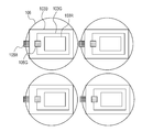
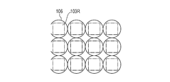
- Fig. 2 is a schematic top view of the first embodiment.
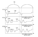
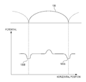
- Fig. 3 is a potential distribution diagram in the horizontal direction of the first embodiment.
- Fig. 4 is a schematic top view of a second embodiment.
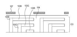
- Fig. 5 is a schematic sectional view of a third embodiment.
- Fig. 6 is a schematic sectional view of a fourth embodiment.
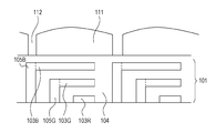
- Fig. 7 is a schematic sectional view of a fifth embodiment.
- Fig. 8A is a schematic sectional view of a sixth embodiment.
- Fig. 8B is a potential distribution diagram in the horizontal direction of the sixth embodiment.
- Fig. 9A is a schematic top view of a seventh embodiment.
- Fig. 9A is a schematic top view of a seventh embodiment.
- FIG. 9B is a schematic top view of photo detectors and microlenses corresponding to blue light according to the seventh embodiment.
- Fig. 9C is a schematic top view of photo detectors and microlenses corresponding to green light according to the seventh embodiment.
- Fig. 9D is a schematic top view of photo detectors and microlenses corresponding to red light according to the seventh embodiment.
- Fig. 10 is a potential distribution diagram in the horizontal direction of the seventh embodiment.
- Fig. 11 is a camera system according to an embodiment.
- electrons are used as signal carriers. Holes may also be used as signal carriers.
- a first conductivity type is an n-type
- a second conductivity type is a p-type.
- the conductivity types of the semiconductor regions are set opposite to those when electrons are signal carriers.
- Fig. 1 is a schematic sectional view of a solid-state image pickup apparatus according to a first embodiment of the present invention.
- Semiconductor regions such as photo detectors and transistors, are included in the semiconductor substrate 101.
- a p-type semiconductor or an SOI substrate may be used as the semiconductor substrate 101.
- a circuit portion 102 is disposed on a first main surface (lower side in the drawing) of the semiconductor substrate 101.
- the circuit portion 102 includes transistors, electrodes, and wires.
- An optical function portion is disposed on a second main surface (upper side in the drawing), i.e., a side opposite to that on which the circuit portion 102 is disposed, with an insulating layer and a protective layer interposed between the optical function portion and the second main surface.
- light enters from the surface opposite to the first main surface (front surface) on which wires and transistors are disposed, i.e., from the second main surface (back surface).
- the optical function portion includes a microlens.
- the microlens functions as a light-level reducing portion.
- n-type semiconductor regions 103B, 103G, and 103R are stacked in the depth direction in the semiconductor substrate 101.
- the depth direction is a direction perpendicular to the front surface or back surface of the substrate.
- the horizontal direction is a direction orthogonal to the depth direction.
- the n-type semiconductor regions 103B, 103G, and 103R each form a p-n junction with a p-type semiconductor region 104.
- the n-type semiconductor region 103B closest to the back surface electrons that are generated through photo-electric conversion of light in the blue wavelength band are mainly collected.
- the n-type semiconductor region 103G disposed deeper than the n-type semiconductor region 103B with respect to the back surface electrons generated through photo-electric conversion of light in the green wavelength band are mainly collected.
- the n-type semiconductor region 103R disposed deepest with respect to the back surface electrons generated through photo-electric conversion of light in the red wavelength band are mainly collected.
- the n-type semiconductor region 103B is equivalent to a first semiconductor region according to the present invention
- the n-type semiconductor region 103G is equivalent to a third semiconductor region according to the present invention.
- each of the n-type semiconductor regions 103B, 103G, and 103R together with the p-type semiconductor region 104 constitute a photo detector, or, specifically, a photodiode.
- each photo detector light in a wavelength region corresponding to the depth of the photo detector is detected.
- N-type semiconductor regions 105B and 105G are readout portions that extract the carriers collected in the n-type semiconductor regions 103B and 103G, respectively.
- the n-type semiconductor region 105B extends in the depth direction of the semiconductor substrate 101 from the n-type semiconductor region 103B to the front surface.
- the n-type semiconductor region 105G extends in the depth direction of the semiconductor substrate 101 from the n-type semiconductor region 103G to the front surface. It is desirable that the impurity concentrations of the n-type semiconductor regions 105B and 105G be respectively higher than those of the n-type semiconductor regions 103B and 103G.
- the n-type semiconductor region 105B is equivalent to a second semiconductor region according to the present invention
- the n-type semiconductor region 105G is equivalent to a fourth semiconductor region according to the present invention.
- the readout portion corresponding to the n-type semiconductor region 103R can be omitted.
- the n-type semiconductor region 103R may also be embedded into the semiconductor substrate 101 such that it is not exposed at the front surface. In such a case, a readout portion corresponding to the n-type semiconductor region 103R should be provided.
- Each readout portion is not limited to such shape and position so long as it has a function for extracting signals based on electrons generated at the photo detectors to the front surface via a readout portion.
- the three n-type semiconductor regions 103B, 103G, and 103R, which are stacked in the depth direction, and the n-type semiconductor regions 105B and 105G are all included in a single pixel. Although only two pixels are illustrated in Fig. 1, actually, multiple pixels are arranged in a line or in a matrix. This is also the true for the other embodiments described below.
- the circuit portion 102 includes a circuit that reads out signals based on electrons generated at the photo detectors. An example configuration of the circuit portion 102 will be described in detail.
- the n-type semiconductor regions 105B and 105G and the n-type semiconductor region 103R are electrically connected with the input of an amplifier via transfer MOS transistors TxB, TxG, and TxR.
- the input of the amplifier can be connected to a power source via a reset MOS transistor Res.
- the amplifier is an amplifier MOS transistor M.
- the gate of the amplifying MOS transistor M is the input.
- One of the source and drain is connected to the power source, and the other is connected to the source or the drain of a selector MOS transistor SEL.
- One of the source and drain of the selector MOS transistor SEL that is not connected to the amplifier MOS transistor M is connected to an output line.
- the configuration is not limited thereto, and the semiconductor regions may be electrically connected directly with the output lines.
- Microlenses 106 that collect light are disposed on the back surface of the semiconductor substrate 101.
- the microlenses 106 are disposed at positions corresponding to the positions of the photo detectors.
- one microlens 106 is disposed for each group of three stacked photo detectors.
- the projection of the microlens 106 in the depth direction covers the photo detectors.
- an edge of the microlens 106 is positioned above the n-type semiconductor region 105B.
- the projection of the microlens 106 in the depth direction overlaps the n-type semiconductor region 105B.
- the microlens 106 may be disposed a certain distance away from the back surface or may be disposed directly on the back surface.
- Incident light converges at the center of the microlens 106. Therefore, the amount of light incident on the n-type semiconductor region 105B disposed below the edge of the microlens 106 is reduced from that when the microlens 106 is not provided.
- the reduction ratio of the amount of incident light is the ratio of the reduction amount by providing the microlens 106 to the amount of the incident light when the microlens 106 is not provided.
- the amount of light incident on the n-type semiconductor region 103B is substantially unchanged or is increased by converging at the microlens 106.
- the reduction ratio is substantially zero, or the amount of incident light does not decrease but, instead, increases.
- the reduction ratio of the amount of incident light on the second semiconductor region is larger than the reduction ratio of the amount of incident light on the first semiconductor region.
- the amount of light incident on the first semiconductor region is not reduced at all or, instead, may be increased.
- the light-level reducing portion may completely block the light incident on the second semiconductor region such that the amount of light incident on the second semiconductor region is zero.
- Fig. 2 is a top view of this embodiment.
- Fig. 2 illustrates the n-type semiconductor regions 103B, 103G, and 103R and the n-type semiconductor regions 105B and 105G.
- the n-type semiconductor regions 103B, 103G, and 103R are overlaid with the microlens 106.
- the edge of the microlens 106 intersects the n-type semiconductor region 105B.
- the projection of the microlens 106 in the depth direction overlaps the n-type semiconductor region 105B.
- the n-type semiconductor region 103B disposed closest to the back surface has the largest area on a horizontal plane.
- the microlens 106 is disposed such that its center substantially matches the center of the n-type semiconductor region 103B.
- Fig. 3 is a potential distribution diagram of this embodiment in the horizontal direction.
- Fig. 3 illustrates the potential distribution in the horizontal direction at depths corresponding to the positions of the n-type semiconductor regions 103B, 103G, and 103R.
- Fig. 3 illustrates the potential distributions along lines A, B, and C in Fig. 1.
- the vertical axis represents the potential of electrons
- the horizontal axis represents the horizontal position.
- a potential barrier formed by the p-type semiconductor region 104 is interposed between the n-type semiconductor regions 103B of adjoining pixels.
- the potential of the n-type semiconductor region 105B which is a readout portion, is lower than the potential of the n-type semiconductor region 103B.
- light mainly in the blue wavelength region is photo-electrically converted and is collected in the n-type semiconductor region 103B as blue signal carriers.
- the n-type semiconductor region 103B When there is a flat section in the potential barrier between the pixels, carriers generated in this flat section diffuses to the depth direction and may enter the n-type semiconductor region 103G. Therefore, it is desirable that the n-type semiconductor region 103B widely extend in the horizontal direction. By reducing the distance between n-type semiconductor regions 103B in adjoining pixels, the flat section in the potential barrier becomes small, and, thus, the electrons reach the n-type semiconductor region 103B more easily than reaching the n-type semiconductor region 103G. That is, color mixing within a pixel can be prevented.
- the microlens 106 is disposed such that its center matches the center of the n-type semiconductor region 103B, and light is allowed to enter the n-type semiconductor region 103B. In this way, the amount of light entering the potential barrier interposed between adjoining pixels decreases, and, as a result, the amount of electrons that may enter the above-described n-type semiconductor region 103G is reduced.
- Fig. 3 illustrates a potential distribution in the horizontal direction at the depth corresponding to the position of the n-type semiconductor region 103G.
- the n-type semiconductor region 105G which is the readout portion, has a potential lower than that of the n-type semiconductor region 103G.
- a potential barrier is formed between the n-type semiconductor region 105G and the n-type semiconductor region 105B. It is desirable that the n-type semiconductor region 105G and the n-type semiconductor region 105B be electrically separated in this way.
- the horizontal positional relationship is such that the edge of the microlens 106 is disposed above the n-type semiconductor region 105B, the amount of light incident on the n-type semiconductor region 105B decreases. Therefore, carriers to be collected as green signal carriers less likely enter the n-type semiconductor region 105B.
- Fig. 3 illustrates a potential distribution in the horizontal direction at a depth corresponding to the position of the n-type semiconductor region 103R.
- potential barriers are formed between the n-type semiconductor region 105B and the n-type semiconductor region 105G, and between the n-type semiconductor region 105G and the n-type semiconductor region 103R. It is desirable that the n-type semiconductor region 105B, the n-type semiconductor region 105G, and the n-type semiconductor region 103R be electrically separated in this way.
- red signal carriers less likely enter the n-type semiconductor region 105B.
- the projection of the edge of the microlens 106 in the depth direction overlaps the n-type semiconductor region 105B.
- the n-type semiconductor region 105B is overlaid with the microlens 106. Since the amount of light incident on the n-type semiconductor region 105B decreases in such a configuration, carriers are less likely generated at a deep position relative to the back surface of the n-type semiconductor region 105B. Consequently, the color separation characteristic is improved.
- the center of the n-type semiconductor region 103B substantially matches the center of the microlens 106 on the horizontal plane. With such a configuration, carriers are less likely generated in the region between the n-type semiconductor regions 103B in adjoining pixels. Consequently, the color separation characteristic is improved.
- FIG. 4 is a top view of the solid-state image pickup apparatus.
- Components that have the same functions as those in the first embodiment will be represented by the same reference numerals, and detailed descriptions thereof will not be repeated.
- the edge of the microlens 106 intersects the n-type semiconductor region 105B and the n-type semiconductor region 105G.
- the microlenses 106 in adjoining pixels are disposed in a connected manner such that they share part of their edge. In this way, when part or all of a microlens 106 is connected with the microlens 106 of the adjoining pixel, a section that appears as a valley in a sectional view also correspond to the edge of the microlens 106. It is desirable that the edge shared by adjoining microlenses 106 be positioned above the n-type semiconductor regions 105B and 105G.
- the amount of light incident on the n-type semiconductor region 105G decreases. Therefore, the amount of carriers generated in the n-type semiconductor region 105G at a depth corresponding to the position of the n-type semiconductor region 103R decreases. That is, carriers to be collected as red signal carriers are less likely collected as green carriers.
- this embodiment has the following advantage.
- the edge of the microlens 106 intersects the n-type semiconductor region 105B and the n-type semiconductor region 105G. Since the amount of light incident on the n-type semiconductor region 105G can be reduced with such a configuration, carriers are less likely generated at a position deep with respect to the back surface of the n-type semiconductor region 105G. Consequently, the color separation characteristic is improved.
- Fig. 5 is a schematic sectional view of a solid-state image pickup apparatus according to another embodiment of the present invention.
- Components that have the same functions as those in the first or second embodiment will be represented by the same reference numerals, and detailed descriptions thereof will not be repeated.
- the configuration according to this embodiment includes light-shielding portions 107 on the back surface, which is the light incident surface. As described below, in this embodiment, the light-shielding portions 107 function as light-level reducing portions.
- the light-shielding portions 107 are made of a material that does not transmit light. For example, a metal such as aluminum is used. Instead, a light-absorbing material, such as black-colored resin, may be used. Each light-shielding portion 107 is disposed above the n-type semiconductor region 105B. The horizontal positional relationship is determined such that the projection of the light-shielding portion 107 in the depth direction overlaps the n-type semiconductor region 105B. The light-shielding portion 107 may be positioned such that at least part of the incident light is blocked.
- the light-shielding portion 107 blocks part of the incident light, and thus, the amount of light incident on the n-type semiconductor region 105B decreases. Photo-electric conversion of light in the green wavelength band and red wavelength band is less likely performed in deep sections of the n-type semiconductor region 105B. As a result, the carriers that should be read out as green or red signal carriers are less likely read out as blue signal carriers.
- the light-shielding portion 107 may be interposed between the n-type semiconductor regions 103B of adjoining pixels. In this way, the amount of light incident on the region between the n-type semiconductor regions 103B of adjoining pixels can be reduced, and thus, the amount of carriers generated at a depth corresponding to the position of the n-type semiconductor region 103B and entering the n-type semiconductor region 103G decreases.
- the projection of the light-shielding portion 107 in the depth direction overlaps the n-type semiconductor region 105B.
- the n-type semiconductor region 105B is overlaid with the light-shielding portion 107. Since the amount of light incident on the n-type semiconductor region 105B can be reduced with such a configuration, the generation of carriers at a deep position with respect to the back surface of the n-type semiconductor region 105B can be suppressed. Consequently, the color separation characteristic is improved.
- the generation of carriers between the n-type semiconductor regions 103B of adjoining pixels can be suppressed. Consequently, the color separation characteristic is improved even more.
- the color separation characteristic can be improved even more.
- Fig. 6 is a schematic sectional view of a solid-state image pickup apparatus according to another embodiment of the present invention.
- Components that have the same functions as those in the first to third embodiments will be represented by the same reference numerals, and detailed descriptions thereof will not be repeated.
- an optical waveguide 108 is disposed on the back surface, which is the light incident surface.
- the optical waveguide 108 according to this embodiment function as a light-level reducing portion.
- the optical waveguide 108 includes a core portion 109 and clad portions 110. It is desirable that the core portion 109 be made of a material that transmits light and has a small index of refraction.
- the clad portions 110 are made of a material that has an index of refraction larger than that of the core portion 109. Instead, a material that reflects light may be used.
- each clad portion 110 is positioned above the n-type semiconductor region 105B.
- the projection of the clad portion 110 in the depth direction overlaps the n-type semiconductor region 105B.
- the directionality of the incident light is improved.
- Light that enters the optical waveguide 108 at a certain incident angle is reflected at and interferes with the clad portions 110.
- the influence of the incident angle is weakened, and the light becomes substantially parallel.
- the solid-state image pickup apparatus including stacked photo detectors will have an unsatisfactory color separation characteristic. Therefore, by using an optical waveguide that is long in the depth direction, the color separation characteristic can be improved.
- the projection of the clad portion 110 in the depth direction overlaps the n-type semiconductor region 105B. That is, when viewed from the top, the n-type semiconductor region 105B is overlaid with the clad portion 110. Since the amount of light incident on the n-type semiconductor region 105B can be reduced with such a configuration, the generation of carriers at a deep position with respect to the back surface of the n-type semiconductor region 105B can be suppressed. Consequently, the color separation characteristic is improved.
- the color separation characteristic can be improved even more.
- Fig. 7 is a schematic sectional view of a solid-state image pickup apparatus according to another embodiment of the present invention.
- Components that have the same functions as those in the first to fourth embodiments will be represented by the same reference numerals, and detailed descriptions thereof will not be repeated.
- a pillar-type microlens 111 is disposed on the back surface for each pixel. As described below, in this embodiment, the pillar-type microlenses 111 function as light-level reducing portions.
- An air gap 112 is formed between the microlenses 111 of adjoining pixels.
- the projection of the air gap 112 in the depth direction overlaps the n-type semiconductor region 105B. That is, when viewed from the top, the n-type semiconductor region 105B is overlaid with the air gap 112.
- the air gap 112 is a vacuum or is filled with nitrogen or air.
- the difference in the indices of refraction of the air gap 112 and the pillar-type microlens 111 causes the light incident on the air gap 112 to converge into the microlens 111.
- the air gap 112 is disposed above the n-type semiconductor region 105B, the amount of light incident on the n-type semiconductor region 105B can be reduced. Therefore, photo-electric conversion of light in the green wavelength band and red wavelength band is less likely performed in deep sections of the n-type semiconductor region 105B. As a result, the carriers that should be read out as green or red signal carriers are less likely read out as blue signal carriers.
- the microlens 111 is pillar-type, the directionality of the incident light is improved. Light that enters the microlens 111 at a certain incident angle is reflected at and interferes with the air gap 112. When the light reaches the second main surface of the semiconductor substrate, the influence of the incident angle is weakened, and the light becomes substantially parallel.
- the solid-state image pickup apparatus including stacked photo detectors will have an unsatisfactory color separation characteristic. Therefore, by using microlenses having excellent directionality of light, the color separation characteristic can be improved.
- the projection of the air gap 112 formed between the pillar-type microlenses in the depth direction overlaps the n-type semiconductor region 105B. That is, when viewed from the top, the n-type semiconductor region 105B is overlaid with the air gap 112.
- the amount of light incident on the n-type semiconductor region 105B can be reduced with such a configuration, the generation of carriers in a deep position with respect to the back surface of the n-type semiconductor region 105B can be suppressed. Consequently, the color separation characteristic is improved.
- the color separation characteristic is improved even more.
- Fig. 8A is a schematic sectional view of a solid-state image pickup apparatus according to another embodiment of the present invention.
- Components that have the same functions as those in the first to fifth embodiments will be represented by the same reference numerals, and detailed descriptions thereof will not be repeated.
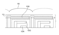
- the n-type semiconductor regions 103B of adjoining pixels are electrically conductive.
- the n-type semiconductor regions 103B may be electrically conductive when a p-type semiconductor region is not provided between the n-type semiconductor regions 103B. Even when a p-type semiconductor region is provided, the n-type semiconductor regions 103B may be electrically conductive when the n-type semiconductor regions 103B are sufficiently close to each other and connected with a depletion layer.
- a depletion layer 113 extending from the n-type semiconductor regions 103B is indicated by dotted lines. As illustrated in Fig. 8A, the n-type semiconductor regions 103B of adjoining pixels are electrically conductive via the depletion layer 113.
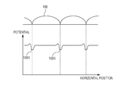
- Fig. 8B illustrates a potential distribution in the horizontal direction at a depth corresponding to the position of the n-type semiconductor regions 103B. That is, Fig. 8B illustrates the potential distribution along line D in Fig. 8A.
- the vertical axis represents the potential of electrons
- the horizontal axis represents the horizontal position.
- a potential barrier formed between the n-type semiconductor regions 103B of two different pixels does not have a flat section.
- the potential barrier formed between the n-type semiconductor regions 103B of two different pixels has a potential gradient that causes carriers to drift toward one of the pixels in the horizontal direction.
- Fig. 8A illustrates microlenses 106, which are similar to those of the first embodiment, disposed on the back surface.
- the configuration is not limited thereto, and configurations of other embodiments may be employed.
- this embodiment has the following advantage.
- the n-type semiconductor regions 103B of adjoining pixels are electrically conductive. With such a configuration, carriers that are generated between the n-type semiconductor regions 103B of adjoining pixels less likely enter the n-type semiconductor regions 103G. Consequently, the color separation characteristic is improved even more.
- the n-type semiconductor regions 103B are electrically conductive.
- the n-type semiconductor regions 103G of adjoining pixels may be electrically conductive in a similar manner. In such a case, carriers that are generated in the region between the n-type semiconductor regions 103G of adjoining pixels less likely enter the n-type semiconductor regions 103B and the n-type semiconductor regions 103R.
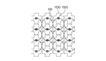
- Fig. 9A is a top view of a solid-state image pickup apparatus according to another embodiment of the present invention.
- Components that have the same functions as those in the first to sixth embodiments will be represented by the same reference numerals, and detailed descriptions thereof will not be repeated.
- the edge of the microlens 106 intersects the center of the n-type semiconductor region 103B.
- the edge of the microlens 106 intersects the center of the n-type semiconductor region 103G.
- one microlens 106 is disposed above two n-type semiconductor regions 103B. That is, the projection of the microlens 106 in the depth direction overlaps two of the n-type semiconductor regions 103B. This is also the same for the n-type semiconductor regions 103G.
- the n-type semiconductor regions 105B and 105G which are readout portions, are disposed at the centers of the n-type semiconductor regions 103B and 103G, respectively. In other words, the projection of the edge of the microlens 106 in the depth direction intersects the n-type semiconductor regions 105B and 105G.
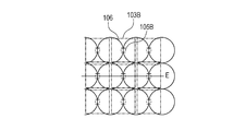
- Fig. 9B is a top view of the microlenses 106, the n-type semiconductor regions 103B, and the n-type semiconductor regions 105B. As illustrated in Fig. 9B, each microlens 106 overlaps two n-type semiconductor region 103B adjoining each other in the left-to-right direction in the drawing. When viewed from the top, the edge of one microlens 106 intersects two n-type semiconductor regions 105B.
- Fig. 9C is a top view of the microlenses 106, the n-type semiconductor regions 103G, and the n-type semiconductor regions 105G.
- the n-type semiconductor regions 103G surround the areas where the n-type semiconductor regions 105B are provided.
- Each microlens 106 overlaps two n-type semiconductor regions 103G adjoining each other in the top-to-bottom direction in the drawing. When viewed from the top, the edge of one microlens 106 intersects two n-type semiconductor regions 105G.
- Fig. 9D is a top view of the microlenses 106 and the n-type semiconductor regions 103R. As illustrated in Fig. 9D, the centers of the microlenses 106 match the centers of the n-type semiconductor regions 103R.
- the n-type semiconductor regions 105B and 105G are disposed at the centers of the n-type semiconductor regions 103B 103G, respectively.
- the n-type semiconductor regions 105B and the n-type semiconductor regions 103G are positioned such that they form a tetragonal face-centered lattice. That is, four n-type semiconductor regions 105B are positioned at the apices of a regular tetragon with one n-type semiconductor region 105G positioned at the center.
- Each of the four n-type semiconductor regions 105B are also positioned at the center of a regular tetragon with four n-type semiconductor regions 105G at the apices.
- the peripheral pixels are not limited such positional relationship.
- the distance between adjoining readout portions can be increased. It is desirable that the impurity concentration of the n-type semiconductor regions 105B and 105G, which are readout portions, be high. When impurity concentration is high, impurities diffuse more easily. Furthermore, a high impurity concentration increases the spreading of the depletion layer in the p-type semiconductor region 104 in the vicinity. Accordingly, when the distance between the n-type semiconductor region 105B and the n-type semiconductor region 105G is small, these regions may become electrically conductive. Thus, it is desirable that the distance between adjoining readout portions be large.
- Fig. 10 illustrates the potential distribution in the horizontal direction along line E in Fig. 9B and at a depth corresponding to the position of the n-type semiconductor regions 103B.
- the vertical axis represents the potential of electrons
- the horizontal axis represents the horizontal position.
- two of the n-type semiconductor regions 103B are disposed below one microlens 106. Therefore, a potential barrier formed between adjoining n-type semiconductor regions 103B is positioned below the microlens 106. In Fig. 10, the potential barrier is positioned at the center of the microlens 106. When light focused by the microlens 106 is photo-electrically converted, the generated carriers are collected to one of the adjoining n-type semiconductor regions 103B on the left and right sides in Fig. 10.
- one microlens 106 corresponds to one pixel.
- the average value of signals from adjoining n-type semiconductor regions 103B on the left and right sides in Fig. 9B may be determined.
- the average value of signals from adjoining n-type semiconductor regions 103G on the upper and lower sides in Fig. 9C may be determined.
- a pixel includes two n-type semiconductor regions 103B while sharing them with the pixels on the left and right.
- a pixel includes two n-type semiconductor regions 103G while sharing them with the pixels above and below.
- the edge of the microlens 106 intersects the n-type semiconductor regions 105B and 105G, which are readout portions. With such a configuration, each pixel shares readout portions with adjoining pixels.
- Figs. 9A, 9B, 9C, 9D, and 10 illustrate a configuration in which microlenses 106, which are similar to those in the first embodiment, are disposed on the back surface. This embodiment is not limited thereto and may employ other embodiments.
- this embodiment has the following advantage.
- the distance between the n-type semiconductor regions 105B and 105G can be set large. With such a configuration, the electric conductivity between the n-type semiconductor regions 105B and 105G can be reduced, and thus, the color separation characteristic is improved even more.
- FIG. 11 is a block diagram illustrating an example image pickup system in which a photoelectric conversion apparatus is applied to a digital still camera.
- Fig. 11 illustrates a barrier 1 that protects a lens 2, which forms an optical image of a subject on a solid-state image pickup apparatus 4, and an aperture stop 3 that varies the amount of light transmitted through the lens 2.
- the solid-state image pickup apparatus 4 is solid-state image pickup apparatuses of one of the embodiments described above and converts an optical image formed by the 2 to image data.
- the substrate of the solid-state image pickup apparatus 4 is provided with an A/D converter.
- a signal processing unit 7 performs various corrections on image pickup data output from the solid-state image pickup apparatus 4 and compresses data.
- FIG. 11 also illustrates a timing generator 8 that outputs various timing signals to the solid-state image pickup apparatus 4 and the signal processing unit 7, and a total control/computation unit 9 that performs various computations and controls the entire digital still camera.
- Image data is temporarily stored in a memory 10.
- An interface unit 11 is used to record to and read out from a recording medium.
- a detachable recording medium such as a semiconductor memory, is used to record and read out image pickup data.
- An interface unit 13 is used to communicate with an external computer, etc.
- the timing signals may be input from a unit outside the image pickup system, so long as the image pickup system includes at least the solid-state image pickup apparatus 4 and the signal processing unit 7 that processes the image pickup signal output from the solid-state image pickup apparatus 4.
- the solid-state image pickup apparatus 4 and the A/D converter are provided on the same substrate.
- the solid-state image pickup apparatus 4 and the A/D converter may be provided on separate substrates.
- the solid-state image pickup apparatus 4 and the signal processing unit 7 may be provided on the same substrate.
- the solid-state image pickup apparatus can be applied to a camera system.
- an image having improved color separation characteristic can be captured.
- a solid-state image pickup apparatus having three photo detectors is described.
- the present invention can be applied so long as a plurality of stacked photo detectors is included.
- the present invention can be applied to a back-illuminated solid-state image pickup apparatus having two stacked photo detectors.
Landscapes
- Physics & Mathematics (AREA)
- Engineering & Computer Science (AREA)
- Power Engineering (AREA)
- Electromagnetism (AREA)
- Condensed Matter Physics & Semiconductors (AREA)
- General Physics & Mathematics (AREA)
- Computer Hardware Design (AREA)
- Microelectronics & Electronic Packaging (AREA)
- Solid State Image Pick-Up Elements (AREA)
- Transforming Light Signals Into Electric Signals (AREA)
- Color Television Image Signal Generators (AREA)
Priority Applications (3)
| Application Number | Priority Date | Filing Date | Title |
|---|---|---|---|
| CN201080056463.XA CN102652359B (zh) | 2009-12-18 | 2010-12-13 | 固态图像拾取设备 |
| US13/515,786 US9245919B2 (en) | 2009-12-18 | 2010-12-13 | Solid-state image pickup apparatus |
| US14/972,510 US9865631B2 (en) | 2009-12-18 | 2015-12-17 | Solid-state image pickup apparatus |
Applications Claiming Priority (2)
| Application Number | Priority Date | Filing Date | Title |
|---|---|---|---|
| JP2009288461A JP5566093B2 (ja) | 2009-12-18 | 2009-12-18 | 固体撮像装置 |
| JP2009-288461 | 2009-12-18 |
Related Child Applications (2)
| Application Number | Title | Priority Date | Filing Date |
|---|---|---|---|
| US13/515,786 A-371-Of-International US9245919B2 (en) | 2009-12-18 | 2010-12-13 | Solid-state image pickup apparatus |
| US14/972,510 Continuation US9865631B2 (en) | 2009-12-18 | 2015-12-17 | Solid-state image pickup apparatus |
Publications (1)
| Publication Number | Publication Date |
|---|---|
| WO2011074234A1 true WO2011074234A1 (en) | 2011-06-23 |
Family
ID=43640626
Family Applications (1)
| Application Number | Title | Priority Date | Filing Date |
|---|---|---|---|
| PCT/JP2010/007224 WO2011074234A1 (en) | 2009-12-18 | 2010-12-13 | Solid-state image pickup apparatus |
Country Status (4)
| Country | Link |
|---|---|
| US (2) | US9245919B2 (zh) |
| JP (1) | JP5566093B2 (zh) |
| CN (2) | CN102652359B (zh) |
| WO (1) | WO2011074234A1 (zh) |
Cited By (1)
| Publication number | Priority date | Publication date | Assignee | Title |
|---|---|---|---|---|
| US9773827B2 (en) * | 2011-10-03 | 2017-09-26 | Canon Kabushiki Kaisha | Solid-state image sensor and camera where the plurality of pixels form a pixel group under a single microlens |
Families Citing this family (12)
| Publication number | Priority date | Publication date | Assignee | Title |
|---|---|---|---|---|
| JP4759590B2 (ja) * | 2008-05-09 | 2011-08-31 | キヤノン株式会社 | 光電変換装置及びそれを用いた撮像システム |
| JP5566093B2 (ja) * | 2009-12-18 | 2014-08-06 | キヤノン株式会社 | 固体撮像装置 |
| TWI427783B (zh) * | 2011-10-28 | 2014-02-21 | Ti Shiue Biotech Inc | 應用於分子檢測與鑑別的多接面結構之光二極體及其製造方法 |
| JP2015076569A (ja) * | 2013-10-11 | 2015-04-20 | ソニー株式会社 | 撮像装置およびその製造方法ならびに電子機器 |
| EP2940504B1 (en) | 2014-04-25 | 2023-06-07 | Personal Genomics, Inc. | Optical sensor |
| JP6444066B2 (ja) * | 2014-06-02 | 2018-12-26 | キヤノン株式会社 | 光電変換装置および撮像システム |
| CN107409184B (zh) * | 2015-03-13 | 2020-09-18 | 索尼半导体解决方案公司 | 固态成像元件、驱动方法以及电子设备 |
| JP6746301B2 (ja) | 2015-11-30 | 2020-08-26 | キヤノン株式会社 | 撮像装置の駆動方法、撮像装置、撮像システム |
| JP6691101B2 (ja) * | 2017-01-19 | 2020-04-28 | ソニーセミコンダクタソリューションズ株式会社 | 受光素子 |
| CN110164909B (zh) * | 2018-04-24 | 2021-03-16 | 京东方科技集团股份有限公司 | 显示基板及其制备方法、显示装置 |
| US10475840B1 (en) * | 2018-10-02 | 2019-11-12 | Foveon, Inc. | Imaging array having improved surface-to-detector light transmission |
| US20220223643A1 (en) | 2021-01-14 | 2022-07-14 | Imec Vzw | Image sensor comprising stacked photo-sensitive devices |
Citations (7)
| Publication number | Priority date | Publication date | Assignee | Title |
|---|---|---|---|---|
| US20030193586A1 (en) * | 2002-04-11 | 2003-10-16 | Canon Kabushiki Kaisha | Image pickup apparatus |
| US20040178463A1 (en) * | 2002-03-20 | 2004-09-16 | Foveon, Inc. | Vertical color filter sensor group with carrier-collection elements of different size and method for fabricating such a sensor group |
| US20060033131A1 (en) * | 2004-08-11 | 2006-02-16 | Dongbuanam Semiconductor Inc. | Complementary metal oxide semiconductor image sensor and method for fabricating the same |
| WO2008026660A1 (fr) * | 2006-09-01 | 2008-03-06 | Sharp Kabushiki Kaisha | Dispositif à semi-conducteur de capture d'image et appareil d'informations électronique |
| US20080265352A1 (en) * | 2007-04-03 | 2008-10-30 | Sharp Kabushiki Kaisha | Solid-state image capturing apparatus, method for manufacturing the same, and electronic information device |
| US20090166518A1 (en) * | 2007-12-28 | 2009-07-02 | Hiok-Nam Tay | Light guide array for an image sensor |
| JP2009288461A (ja) | 2008-05-28 | 2009-12-10 | Nec Electronics Corp | 表示装置、表示パネルドライバ、表示パネルの駆動方法、及び表示パネルドライバへの画像データ供給方法 |
Family Cites Families (30)
| Publication number | Priority date | Publication date | Assignee | Title |
|---|---|---|---|---|
| JPS61135280A (ja) * | 1984-12-06 | 1986-06-23 | Toshiba Corp | 三次元撮像素子 |
| US6864557B2 (en) * | 2001-06-18 | 2005-03-08 | Foveon, Inc. | Vertical color filter detector group and array |
| US7129466B2 (en) * | 2002-05-08 | 2006-10-31 | Canon Kabushiki Kaisha | Color image pickup device and color light-receiving device |
| JP2004356207A (ja) * | 2003-05-27 | 2004-12-16 | Fujio Masuoka | 半導体記憶装置及びその製造方法 |
| JP4432502B2 (ja) | 2004-01-20 | 2010-03-17 | ソニー株式会社 | 半導体装置 |
| JP4779304B2 (ja) * | 2004-03-19 | 2011-09-28 | ソニー株式会社 | 固体撮像素子、カメラモジュール及び電子機器モジュール |
| CN100505321C (zh) | 2004-05-27 | 2009-06-24 | 佛文恩股份有限公司 | 含非晶硅半导体的垂直滤色片传感器组及其制造方法 |
| US20060066131A1 (en) * | 2004-08-11 | 2006-03-30 | Nebel Michael W | Bedlift with chain lift system for toy trailer |
| US7242027B2 (en) * | 2004-08-13 | 2007-07-10 | Paul Steven Schranz | Light emitting and image sensing device and apparatus |
| JP2007066962A (ja) * | 2005-08-29 | 2007-03-15 | Fujifilm Corp | カラー固体撮像装置及びデジタルカメラ |
| JP4823619B2 (ja) * | 2005-09-12 | 2011-11-24 | ルネサスエレクトロニクス株式会社 | 光電変換素子、固定撮像デバイス、撮像装置、および画像読み取り装置 |
| KR100698099B1 (ko) * | 2005-09-13 | 2007-03-23 | 동부일렉트로닉스 주식회사 | 씨모스 이미지 센서 및 그 제조방법 |
| KR100660348B1 (ko) * | 2005-12-28 | 2006-12-22 | 동부일렉트로닉스 주식회사 | Cmos 이미지 센서의 제조방법 |
| US7705288B2 (en) * | 2006-03-31 | 2010-04-27 | Hand Held Products, Inc. | Optical reading device with light blocking gasket |
| JP2008270679A (ja) * | 2007-04-25 | 2008-11-06 | Sony Corp | 固体撮像装置およびその製造方法および撮像装置 |
| TWI479887B (zh) * | 2007-05-24 | 2015-04-01 | Sony Corp | 背向照明固態成像裝置及照相機 |
| JP2009059824A (ja) * | 2007-08-30 | 2009-03-19 | Sharp Corp | 固体撮像素子およびその製造方法、電子情報機器 |
| JP4858367B2 (ja) | 2007-09-10 | 2012-01-18 | ソニー株式会社 | 固体撮像素子の製造方法 |
| JP5364989B2 (ja) * | 2007-10-02 | 2013-12-11 | ソニー株式会社 | 固体撮像装置およびカメラ |
| JP4609497B2 (ja) * | 2008-01-21 | 2011-01-12 | ソニー株式会社 | 固体撮像装置とその製造方法、及びカメラ |
| KR20090108233A (ko) * | 2008-04-11 | 2009-10-15 | 삼성전자주식회사 | 카메라 모듈의 제조 방법, 이에 의해 제작된 카메라 모듈및 상기 카메라 모듈을 포함하는 전자 시스템 |
| JP5369505B2 (ja) | 2008-06-09 | 2013-12-18 | ソニー株式会社 | 固体撮像装置、及び電子機器 |
| US8207590B2 (en) * | 2008-07-03 | 2012-06-26 | Samsung Electronics Co., Ltd. | Image sensor, substrate for the same, image sensing device including the image sensor, and associated methods |
| JP4905468B2 (ja) | 2009-01-09 | 2012-03-28 | ソニー株式会社 | 固体撮像素子 |
| US8816460B2 (en) * | 2009-04-06 | 2014-08-26 | Nokia Corporation | Image sensor |
| US20100330728A1 (en) * | 2009-06-26 | 2010-12-30 | Mccarten John P | Method of aligning elements in a back-illuminated image sensor |
| JP5564847B2 (ja) | 2009-07-23 | 2014-08-06 | ソニー株式会社 | 固体撮像装置とその製造方法、及び電子機器 |
| JP5566093B2 (ja) * | 2009-12-18 | 2014-08-06 | キヤノン株式会社 | 固体撮像装置 |
| JP5651986B2 (ja) * | 2010-04-02 | 2015-01-14 | ソニー株式会社 | 固体撮像装置とその製造方法、並びに電子機器及びカメラモジュール |
| JP5817301B2 (ja) * | 2011-08-02 | 2015-11-18 | ソニー株式会社 | 撮像素子、並びに、撮像装置および方法 |
-
2009
- 2009-12-18 JP JP2009288461A patent/JP5566093B2/ja not_active Expired - Fee Related
-
2010
- 2010-12-13 CN CN201080056463.XA patent/CN102652359B/zh not_active Expired - Fee Related
- 2010-12-13 CN CN201510124447.4A patent/CN104701335A/zh active Pending
- 2010-12-13 WO PCT/JP2010/007224 patent/WO2011074234A1/en active Application Filing
- 2010-12-13 US US13/515,786 patent/US9245919B2/en not_active Expired - Fee Related
-
2015
- 2015-12-17 US US14/972,510 patent/US9865631B2/en not_active Expired - Fee Related
Patent Citations (8)
| Publication number | Priority date | Publication date | Assignee | Title |
|---|---|---|---|---|
| US20040178463A1 (en) * | 2002-03-20 | 2004-09-16 | Foveon, Inc. | Vertical color filter sensor group with carrier-collection elements of different size and method for fabricating such a sensor group |
| US20030193586A1 (en) * | 2002-04-11 | 2003-10-16 | Canon Kabushiki Kaisha | Image pickup apparatus |
| US20060033131A1 (en) * | 2004-08-11 | 2006-02-16 | Dongbuanam Semiconductor Inc. | Complementary metal oxide semiconductor image sensor and method for fabricating the same |
| WO2008026660A1 (fr) * | 2006-09-01 | 2008-03-06 | Sharp Kabushiki Kaisha | Dispositif à semi-conducteur de capture d'image et appareil d'informations électronique |
| JP2008060476A (ja) | 2006-09-01 | 2008-03-13 | Sharp Corp | 固体撮像装置および電子情報機器 |
| US20080265352A1 (en) * | 2007-04-03 | 2008-10-30 | Sharp Kabushiki Kaisha | Solid-state image capturing apparatus, method for manufacturing the same, and electronic information device |
| US20090166518A1 (en) * | 2007-12-28 | 2009-07-02 | Hiok-Nam Tay | Light guide array for an image sensor |
| JP2009288461A (ja) | 2008-05-28 | 2009-12-10 | Nec Electronics Corp | 表示装置、表示パネルドライバ、表示パネルの駆動方法、及び表示パネルドライバへの画像データ供給方法 |
Cited By (3)
| Publication number | Priority date | Publication date | Assignee | Title |
|---|---|---|---|---|
| US9773827B2 (en) * | 2011-10-03 | 2017-09-26 | Canon Kabushiki Kaisha | Solid-state image sensor and camera where the plurality of pixels form a pixel group under a single microlens |
| US10504947B2 (en) | 2011-10-03 | 2019-12-10 | Canon Kabushiki Kaisha | Solid-state image sensor and camera |
| US11348953B2 (en) | 2011-10-03 | 2022-05-31 | Canon Kabushiki Kaisha | Solid-state image sensor and camera |
Also Published As
| Publication number | Publication date |
|---|---|
| CN102652359A (zh) | 2012-08-29 |
| CN104701335A (zh) | 2015-06-10 |
| JP2011129785A (ja) | 2011-06-30 |
| CN102652359B (zh) | 2015-04-08 |
| US20120298841A1 (en) | 2012-11-29 |
| US20160104728A1 (en) | 2016-04-14 |
| JP5566093B2 (ja) | 2014-08-06 |
| US9245919B2 (en) | 2016-01-26 |
| US9865631B2 (en) | 2018-01-09 |
Similar Documents
| Publication | Publication Date | Title |
|---|---|---|
| US9865631B2 (en) | Solid-state image pickup apparatus | |
| KR102577844B1 (ko) | 이미지 센서 | |
| US9548328B2 (en) | Solid-state image sensor and camera | |
| US7075164B2 (en) | Semiconductor photoelectric conversion device suitable for miniaturization | |
| US8638382B2 (en) | Solid-state imaging device and electronic apparatus | |
| US7535073B2 (en) | Solid-state imaging device, camera module and electronic equipment module | |
| US8243176B2 (en) | Solid-state image sensor | |
| JP4751865B2 (ja) | 裏面照射型固体撮像素子及びその製造方法 | |
| JP2008227250A (ja) | 複合型固体撮像素子 | |
| US10734433B2 (en) | Solid-state imaging device | |
| US8860102B2 (en) | Solid state imaging device and imaging apparatus | |
| US20130049156A1 (en) | Solid-state imaging apparatus | |
| JP4696104B2 (ja) | 裏面照射型固体撮像素子及びその製造方法 | |
| US20200075660A1 (en) | Solid-state image pickup device | |
| JP6086715B2 (ja) | 固体撮像素子 | |
| JP6230637B2 (ja) | 固体撮像装置 | |
| US12068347B2 (en) | Solid-state imaging device and electronic device | |
| JP5885779B2 (ja) | 固体撮像装置 | |
| US20220139989A1 (en) | Image sensor | |
| JP5563179B1 (ja) | 固体撮像装置 | |
| KR20120120669A (ko) | Cmos 이미지 센서 | |
| JP2009130305A (ja) | 固体撮像装置 |
Legal Events
| Date | Code | Title | Description |
|---|---|---|---|
| WWE | Wipo information: entry into national phase |
Ref document number: 201080056463.X Country of ref document: CN |
|
| 121 | Ep: the epo has been informed by wipo that ep was designated in this application |
Ref document number: 10805841 Country of ref document: EP Kind code of ref document: A1 |
|
| WWE | Wipo information: entry into national phase |
Ref document number: 13515786 Country of ref document: US |
|
| NENP | Non-entry into the national phase |
Ref country code: DE |
|
| 122 | Ep: pct application non-entry in european phase |
Ref document number: 10805841 Country of ref document: EP Kind code of ref document: A1 |

