WO2011065133A1 - 光電変換素子用材料及び光電変換素子 - Google Patents
光電変換素子用材料及び光電変換素子 Download PDFInfo
- Publication number
- WO2011065133A1 WO2011065133A1 PCT/JP2010/067826 JP2010067826W WO2011065133A1 WO 2011065133 A1 WO2011065133 A1 WO 2011065133A1 JP 2010067826 W JP2010067826 W JP 2010067826W WO 2011065133 A1 WO2011065133 A1 WO 2011065133A1
- Authority
- WO
- WIPO (PCT)
- Prior art keywords
- group
- photoelectric conversion
- phthalocyanine
- conversion element
- substituent
- Prior art date
- Legal status (The legal status is an assumption and is not a legal conclusion. Google has not performed a legal analysis and makes no representation as to the accuracy of the status listed.)
- Ceased
Links
Images



Classifications
-
- B—PERFORMING OPERATIONS; TRANSPORTING
- B82—NANOTECHNOLOGY
- B82Y—SPECIFIC USES OR APPLICATIONS OF NANOSTRUCTURES; MEASUREMENT OR ANALYSIS OF NANOSTRUCTURES; MANUFACTURE OR TREATMENT OF NANOSTRUCTURES
- B82Y10/00—Nanotechnology for information processing, storage or transmission, e.g. quantum computing or single electron logic
-
- H—ELECTRICITY
- H10—SEMICONDUCTOR DEVICES; ELECTRIC SOLID-STATE DEVICES NOT OTHERWISE PROVIDED FOR
- H10K—ORGANIC ELECTRIC SOLID-STATE DEVICES
- H10K85/00—Organic materials used in the body or electrodes of devices covered by this subclass
- H10K85/30—Coordination compounds
- H10K85/311—Phthalocyanine
-
- H—ELECTRICITY
- H10—SEMICONDUCTOR DEVICES; ELECTRIC SOLID-STATE DEVICES NOT OTHERWISE PROVIDED FOR
- H10K—ORGANIC ELECTRIC SOLID-STATE DEVICES
- H10K30/00—Organic devices sensitive to infrared radiation, light, electromagnetic radiation of shorter wavelength or corpuscular radiation
- H10K30/30—Organic devices sensitive to infrared radiation, light, electromagnetic radiation of shorter wavelength or corpuscular radiation comprising bulk heterojunctions, e.g. interpenetrating networks of donor and acceptor material domains
- H10K30/35—Organic devices sensitive to infrared radiation, light, electromagnetic radiation of shorter wavelength or corpuscular radiation comprising bulk heterojunctions, e.g. interpenetrating networks of donor and acceptor material domains comprising inorganic nanostructures, e.g. CdSe nanoparticles
- H10K30/352—Organic devices sensitive to infrared radiation, light, electromagnetic radiation of shorter wavelength or corpuscular radiation comprising bulk heterojunctions, e.g. interpenetrating networks of donor and acceptor material domains comprising inorganic nanostructures, e.g. CdSe nanoparticles the inorganic nanostructures being nanotubes or nanowires, e.g. CdTe nanotubes in P3HT polymer
-
- H—ELECTRICITY
- H10—SEMICONDUCTOR DEVICES; ELECTRIC SOLID-STATE DEVICES NOT OTHERWISE PROVIDED FOR
- H10K—ORGANIC ELECTRIC SOLID-STATE DEVICES
- H10K30/00—Organic devices sensitive to infrared radiation, light, electromagnetic radiation of shorter wavelength or corpuscular radiation
- H10K30/50—Photovoltaic [PV] devices
-
- H—ELECTRICITY
- H10—SEMICONDUCTOR DEVICES; ELECTRIC SOLID-STATE DEVICES NOT OTHERWISE PROVIDED FOR
- H10K—ORGANIC ELECTRIC SOLID-STATE DEVICES
- H10K85/00—Organic materials used in the body or electrodes of devices covered by this subclass
- H10K85/20—Carbon compounds, e.g. carbon nanotubes or fullerenes
- H10K85/211—Fullerenes, e.g. C60
- H10K85/215—Fullerenes, e.g. C60 comprising substituents, e.g. PCBM
-
- Y—GENERAL TAGGING OF NEW TECHNOLOGICAL DEVELOPMENTS; GENERAL TAGGING OF CROSS-SECTIONAL TECHNOLOGIES SPANNING OVER SEVERAL SECTIONS OF THE IPC; TECHNICAL SUBJECTS COVERED BY FORMER USPC CROSS-REFERENCE ART COLLECTIONS [XRACs] AND DIGESTS
- Y02—TECHNOLOGIES OR APPLICATIONS FOR MITIGATION OR ADAPTATION AGAINST CLIMATE CHANGE
- Y02E—REDUCTION OF GREENHOUSE GAS [GHG] EMISSIONS, RELATED TO ENERGY GENERATION, TRANSMISSION OR DISTRIBUTION
- Y02E10/00—Energy generation through renewable energy sources
- Y02E10/50—Photovoltaic [PV] energy
- Y02E10/549—Organic PV cells
-
- Y—GENERAL TAGGING OF NEW TECHNOLOGICAL DEVELOPMENTS; GENERAL TAGGING OF CROSS-SECTIONAL TECHNOLOGIES SPANNING OVER SEVERAL SECTIONS OF THE IPC; TECHNICAL SUBJECTS COVERED BY FORMER USPC CROSS-REFERENCE ART COLLECTIONS [XRACs] AND DIGESTS
- Y10—TECHNICAL SUBJECTS COVERED BY FORMER USPC
- Y10T—TECHNICAL SUBJECTS COVERED BY FORMER US CLASSIFICATION
- Y10T428/00—Stock material or miscellaneous articles
- Y10T428/29—Coated or structually defined flake, particle, cell, strand, strand portion, rod, filament, macroscopic fiber or mass thereof
- Y10T428/2913—Rod, strand, filament or fiber
- Y10T428/298—Physical dimension
Definitions
- the principle of photoelectric conversion of organic thin film solar cells is (1) Exciton (hole-electron pair) is generated by light absorption of the organic semiconductor layer, (2) This diffuses and moves to the bonding interface (DA bonding interface) between the electron donating material and the electron accepting material, (3) Charge separation into holes and electrons, (4) Each charge is transported to the positive electrode and the negative electrode through the electron donating material and the electron accepting material to generate electric power, and the photoelectric conversion efficiency is determined by integrating the efficiency of each process. .
- the exciton lifetime is extremely short, and the distance that can be diffused and transferred is extremely short, from several nanometers to several tens of nanometers.
- the present inventor made nanowires of phthalocyanines having excellent durability as an electron donating material and dispersed them in a solvent, whereby a photoelectric conversion element having a nanowire network structure by a wet process.
- the present invention has been completed.
- the present invention relates to a material for a photoelectric conversion element containing a phthalocyanine nanowire having a minor axis of 50 nm or less as an electron donating material and a ratio of the length to the minor axis (length / minor axis) of 10 or more, And a photoelectric conversion element using the material.
- such functional groups include, for example, alkyl groups, alkyloxy groups, amino groups, mercapto groups, carboxy groups, sulfonic acid groups, silyl groups, silanol groups, boronic acid groups, nitro groups, and phosphoric acids.
- An aryl group such as, a heteroaryl group such as an indoyl group and a pyridinyl group, and a meryl group.
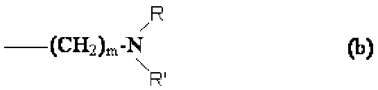
- M is an integer of 1 to 20, and R and R ′ are each independently an alkyl group having 1 to 20 carbon atoms or an aryl group.
- the group represented by can also be used.
- the (oligo) heteroaryl group which may have a substituent is preferably a pyrrole group which may have a substituent, a thiophene group which may have a substituent, or a substituent. Examples thereof include a good oligopyrrole group and an oligothiophene group which may have a substituent. Examples of the substituent include conventionally known substituents that can be substituted on the heteroaryl group.
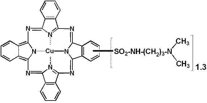
- the phthalocyanine having a substituent represented by the general formula (1) include the following, but are not limited thereto.
- the number next to the parentheses in the formula of the substituted phthalocyanine represents the average number of functional groups introduced into the phthalocyanine molecule. This is because the number of introduced substituents for each molecule is an integer, but in actuality, different numbers of introduced substituents are used in combination.
- phthalocyanines are soluble in an acid solvent such as sulfuric acid.
- an acid solvent such as sulfuric acid.
- the unsubstituted phthalocyanine and the phthalocyanine having the substituent are mixed with sulfuric acid, chlorosulfuric acid.
- an acid solvent such as methanesulfonic acid or trifluoroacetic acid.
- it is poured into a poor solvent such as water to precipitate a complex of the unsubstituted phthalocyanine and the phthalocyanine derivative having the substituent.
- the method is not particularly limited as long as the composite obtained through the step (a) can be made into fine particles, but the composite is made into fine particles by a wet dispersion method.
- a wet disperser using microbeads such as a bead mill or a paint conditioner is used for the composite obtained in the step (a), or T.I. K.
- the composite can be microparticulated by wet dispersion together with a dispersion solvent such as water or an organic solvent and a water-containing organic solvent.
- metal ions examples include all metal ions that can be a central metal of metal phthalocyanine, and specifically include copper ions, zinc ions, cobalt ions, nickel ions, iron ions, and the like. . These metal ions are usually subjected to the reaction by dissolving a metal salt in a water-soluble polyhydric alcohol.
- the salt include halides and sulfates.
- copper chloride (II) and copper sulfate (II) can be mentioned as preferable salts.
- the type of the organic solvent is not particularly limited as long as it can stably disperse phthalocyanine nanowires, and may be a single organic solvent or an organic solvent in which two or more types are mixed. From the viewpoint that nanowires can be dispersed well and stably, amide solvents are preferred, and specifically, N, N-dimethylacetamide, N, N-dimethylformamide, N-methylpyrrolidone, N, N-diethyl For example, N-methylpyrrolidone is particularly preferable.
- the content of phthalocyanine nanowires in the composition is 0.05 to 20% by mass for imparting wet process (printing or coating) suitability and good film formation. In particular, 0.1 to 10% by mass is preferable.
- fullerene compounds are preferably used because of their high charge separation speed and electron transfer speed.
- fullerene compounds PCBM and C70 derivatives (such as the above PC70BM) are more preferable because they are particularly excellent in charge separation rate and electron transfer rate and can provide higher photoelectric conversion efficiency.
- a resin component is added as a rheological adjustment or binder component. can do.
- the resin is not particularly limited as long as it is a publicly known one, and it may be a single resin or two or more resins may be used in combination. Polymethyl methacrylate, polystyrene, polycarbonate, etc. may be used. preferable.
- the photoelectric conversion element of the present invention includes at least a pair of electrodes, that is, a positive electrode and a negative electrode, and the material for the photoelectric conversion element of the present invention formed between these electrodes.
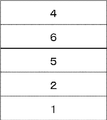
- FIG. 1 is a schematic view showing an example of the photoelectric conversion element of the present invention.
- reference numeral 1 is a substrate
- reference numeral 2 is an electrode a
- reference numeral 3 is a photoelectric conversion layer (organic semiconductor layer) containing the material for a photoelectric conversion element of the present invention
- reference numeral 4 is an electrode b.
- the organic semiconductor layer 3 contains an electron-accepting material
- a phthalocyanine nanowire whose minor axis is 50 nm or less and the ratio of the length to the minor axis (length / minor axis) is 10 or more and the electron-accepting material May be mixed or laminated.
- An example in the case of being laminated is shown in FIG.
- a layer having an electron donating material “a material for a photoelectric conversion element containing a phthalocyanine nanowire having a minor axis of 50 nm or less and a ratio of the length to the minor axis (length / minor axis) of 10 or more”
- the layer having the electron-accepting material is on the negative electrode side. Accordingly, reference numeral 5 in FIG.
- the thickness of the organic semiconductor layer is not particularly limited as long as it is a thickness that can sufficiently absorb light and does not cause charge deactivation. Is preferably in the range of 10 nm to 500 nm, more preferably 20 nm to 300 nm.
- the layer having “the phthalocyanine nanowire whose minor axis is 50 nm or less and the ratio of the length to the minor axis (length / minor axis) is 10 or more” of the present invention has the above thickness. Of these, the thickness is preferably 1 nm to 500 nm, more preferably 15 nm to 300 nm.
- silicon, glass, and various resin materials can be used.
- the various resin materials include polyethylene terephthalate (PET), polyethylene naphthalate (PEN), polyethersulfone (PES), polyetherimide, polyetheretherketone, polyphenylene sulfide, polyarylate, polyimide, polycarbonate (PC), Examples thereof include cellulose triacetate (TAC), cellulose acetate propionate (CAP), and acrylic resin.
- PET polyethylene terephthalate
- PEN polyethylene naphthalate
- PES polyethersulfone
- PES polyetherimide
- polyetheretherketone polyphenylene sulfide
- PC polycarbonate
- TAC cellulose triacetate
- CAP cellulose acetate propionate
- acrylic resin acrylic resin
- An electrode using a conductive material having a small work function serves as a negative electrode.
- the conductive material having a small work function alkali metal or alkaline earth metal, specifically, lithium, magnesium, or calcium is used. Tin, silver, and aluminum are also preferably used.
- an electrode made of an alloy made of the above metal or a laminate of the above metal is also preferably used.
- the conductive material used for the negative electrode is preferably one that is in ohmic contact with the organic semiconductor layer 3. Furthermore, when the buffer layer 2 described later is used, it is preferable that the conductive material used for the negative electrode is in ohmic contact with the buffer layer 2.
- the electrode a or the electrode b has a light transmittance.
- the light transmittance of the electrode is not particularly limited as long as incident light reaches the organic semiconductor layer 3 and an electromotive force is generated.
- a conductive material for example, ITO (indium oxide-tin oxide composite), FTO (fluorine-doped tin oxide), (laminated) graphene, (laminated) modified graphene, or a known material whose conductivity has been improved by doping.
- Conductive polymers such as conductive polyaniline, conductive polypyrrole, conductive polythiophene, and conductive polyethylene dioxythiophene (PEDOT) are preferably used. In addition, these materials can be used in combination with a mesh made of a metal material having high conductivity.
- a conductive fine particle dispersion or a conductive polymer solution or dispersion may be directly patterned by an ink jet method, a screen method, a gravure offset method, a letterpress inversion method, a microcontact method, or a “solid” coating film.
- the pattern may be formed by lithography, laser ablation, or the like.
- PEDOT polyethylenedioxythiophene
- PSS polystyrene sulfonate
- the thickness of the buffer layer 1 is preferably 5 nm to 600 nm, more preferably 10 nm to 200 nm.
- the buffer layer 2 may be provided between the organic semiconductor layer 3 and the negative electrode.
- the buffer layer 2 is used as necessary to enable efficient charge extraction.
- the above-described electron-accepting materials naphthalenes (1,4,5,8-naphthalenetetracarboxylic diimide (NTCDI), N, N′-dialkyl-1,4,5,8) -Naphthalene tetracarboxyl diimide (NTCDI-R) (R is an alkyl group having 1 to 20 carbon atoms), 1,4,5,8-naphthalene tetracarboxyl dianhydride (NTCDA)), perylenes (3,4 , 9,10-perylenetetracarboxylic dianhydride (PTCDA), 3,4,9,10-perylenetetracarboxylic bisbenzimidazole (PTCBI), 3,4,9,10-perylenetetracarboxylic diimide (PTCDI)
- Buffer layer formation methods include vacuum deposition, molecular beam epitaxial growth, ion cluster beam method, low energy ion beam method, ion plating method, CVD method, sputtering method, atmospheric pressure plasma method, and other dry processes, inkjet Method, gravure method, gravure offset method, offset method, letterpress method, letterpress inversion method, screen method, microcontact method, reverse method, air doctor coater method, blade coater method, air knife coater method, roll coater method, squeeze coater method, Impregnation coater method, transfer roll coater method, kiss coater method, cast coater method, spray coater method, electrostatic coater method, ultrasonic spray coater method, die coater method, spin coater method, bar coater method, slit coater Law, include wet process drop casting, may be appropriately used depending on the material.
- an inorganic oxide for the buffer layer When using an inorganic oxide for the buffer layer, as a wet process, apply a liquid in which fine particles of the inorganic oxide are dispersed in any organic solvent or water using a dispersion aid such as a surfactant as required. Further, a drying method or a so-called sol-gel method in which an oxide precursor, for example, an alkoxide body solution is applied and dried can be used.
- a drying method or a so-called sol-gel method in which an oxide precursor, for example, an alkoxide body solution is applied and dried can be used.
- These buffer layers may be a single layer or a laminate of different materials.
- the photoelectric conversion element by this invention can comprise a solar cell module by integration.
- the photoelectric conversion element of this invention can also be set as the structure which interrupts
- a solar cell module by contacting the electrode a of the photoelectric conversion element according to the present invention and the electrode b of another photoelectric conversion element according to the present invention adjacent thereto, the photoelectric conversion elements according to the present invention are connected in series.
- Example 1 Manufacture of materials for photoelectric conversion elements> -Process (a) (crystallization process) Of 1.67 g of copper phthalocyanine (Fastogen Blue 5380E, manufactured by DIC) and phthalocyanine having a substituent, 0.83 g of the derivative represented by [Chemical Formula 9] is added to 81 g of concentrated sulfuric acid (manufactured by Kanto Chemical) and completely dissolved. To prepare a concentrated sulfuric acid solution.
- the obtained composite was filtered using a filter paper, washed sufficiently with distilled water, and the composite containing water was recovered.
- the weight of this water-containing composite was measured and found to be 12.4 g.
- Step (c) (dispersing step in an organic solvent)
- the finely divided complex obtained in the step (b) was dispersed in 60 g of orthodichlorobenzene, stirred for 2 hours, then added with 60 g of N-methylpyrrolidone, and further stirred for 2 hours.
- the heated dispersion was filtered using a membrane filter (pore size 0.1 ⁇ m), and the residue was thoroughly washed with orthodichlorobenzene.
- the filtered residue was put into orthodichlorobenzene so that the solid concentration would be 2%, and shaken well to obtain an orthodichlorobenzene dispersion (1) containing copper phthalocyanine nanowires.
- the dispersion was very stable and no precipitation of phthalocyanine nanowires was observed.
- the solid content of the dispersion liquid (1) obtained here was observed using a transmission electron microscope, it had a nanowire shape in which the minor axis grew to about 25 nm and the ratio of the length to the minor axis was 20 or more. Was confirmed (see FIGS. 3 and 4). Moreover, since the solid content of the dispersion liquid (1) showed a sharp X-ray diffraction peak, it was confirmed that it had high crystallinity.
- 150 mg of the above dispersion (1), 10 mg of PCBM (manufactured by Frontier Carbon Co., Ltd.) and 350 mg of orthodichlorobenzene are added to a sample bottle and subjected to ultrasonic irradiation for 30 minutes in an ultrasonic cleaner (47 kHz). Material (1) was obtained.
- JV max is the product of the current density and the applied voltage at the point where the product of the current density and the applied voltage is maximum between the applied voltage of 0 V and the open circuit voltage value.
- PCE [(J sc ⁇ V oc ⁇ FF) / pseudo sunlight intensity (100 mW / cm 2 )] ⁇ 100 (%)
- Example 3 ⁇ Production of photoelectric conversion element>
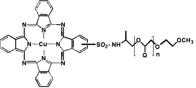
- polyether monoamine 692 parts by mass of Surfamine B-200 (trade name, primary amine-terminated poly (ethylene oxide / propylene oxide) (5/95) copolymer, number average molecular weight of about 2,000, manufactured by Huntsman Corporation) and sodium carbonate
- Surfamine B-200 trade name, primary amine-terminated poly (ethylene oxide / propylene oxide) (5/95) copolymer, number average molecular weight of about 2,000, manufactured by Huntsman Corporation
- the obtained reaction mixture was heated to 90 ° C. under vacuum to remove water to obtain a copper phthalocyanine sulfamoyl compound represented by the following [Chemical Formula 20].
- Photoelectric conversion element material (3) and photoelectric conversion were performed in the same manner as in Example 1 except that the compound represented by [Chemical Formula 20] was used instead of the compound represented by [Chemical Formula 9] in Example 1. Element (3) was produced.
- Example 7 Photoelectric conversion element material (7) and photoelectric conversion were performed in the same manner as in Example 1 except that the compound represented by [Chemical Formula 8] was used instead of the compound represented by [Chemical Formula 9] in Example 1. An element (7) was produced.
Landscapes
- Engineering & Computer Science (AREA)
- Chemical & Material Sciences (AREA)
- Nanotechnology (AREA)
- Physics & Mathematics (AREA)
- Mathematical Physics (AREA)
- Theoretical Computer Science (AREA)
- Crystallography & Structural Chemistry (AREA)
- Inorganic Chemistry (AREA)
- Materials Engineering (AREA)
- Photovoltaic Devices (AREA)
- Nitrogen Condensed Heterocyclic Rings (AREA)
- Inks, Pencil-Leads, Or Crayons (AREA)
Abstract
Description
(1)環境負荷が少ない
(2)製造コストが安い
(3)軽量で壊れにくい
等の点でポテンシャルが高く、近年注目を集めている。有機薄膜太陽電池とは、ポリチオフェン系やポリフェニレンビニレン系などの電子供与性π共役系ポリマーやフタロシアニン類などの電子供与性低分子材料と、フラーレン類などの電子受容性材料からなる有機半導体層を光電変換の活性層(光電変換層)とした、有機材料で構成される光電変換素子のことである。最近は、特に、電子供与性材料と電子受容性材料とをナノレベルでコンポジット化して、光電変換に寄与する両材料の接合界面(DA接合界面)を増大させたバルクヘテロ接合型の開発が活発に行われている(特許文献1)。
(1)有機半導体層の光吸収により励起子(正孔・電子の対)が生じ、
(2)これが電子供与性材料と電子受容性材料の接合界面(DA接合界面)に拡散移動して、
(3)正孔及び電子に電荷分離し、
(4)それぞれの電荷が電子供与性材料及び電子受容性材料を通じて、正極及び負極に電荷輸送されて電力を発生するものであり、前記各過程の効率の積算でその光電変換効率が決定される。ここで励起子の寿命は極めて短く、拡散移動できる距離はせいぜい数ナノメートルから十数ナノメートルと極めて短いため、光電変換の効率を高めるためには、有機半導体層中のDA接合界面が前記の励起子の拡散移動可能な距離と同程度の距離範囲内に存在していることが好ましく、かつ、電荷分離後の電荷がそれぞれの電極へ速やかに移動できる電荷輸送経路が確保されていることが好ましい。
本発明の光電変換素子用材料は、短径が50nm以下であってその短径に対する長さの比率(長さ/短径)が10以上であるフタロシアニンナノワイヤを含有する。以下、本発明に用いるフタロシアニンナノワイヤについて説明する。
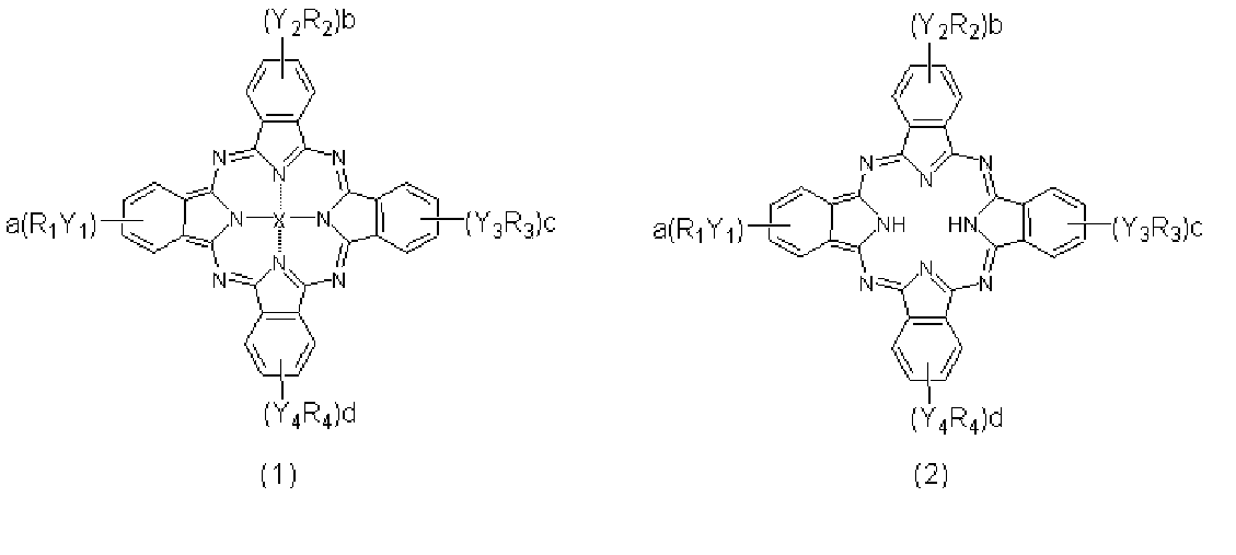
一般式(1)又は(2)において、R1~R4は、上記結合基Y1からY4を介してフタロシアニン環と結合しえる官能基である。

で表される基も用いることができる。

で表される基を挙げることができる。置換基としては、フタルイミド基に置換が可能な通常公知の置換基を挙げることができる。


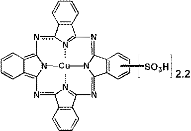
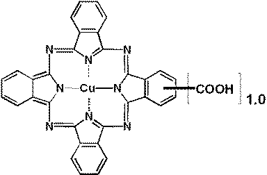
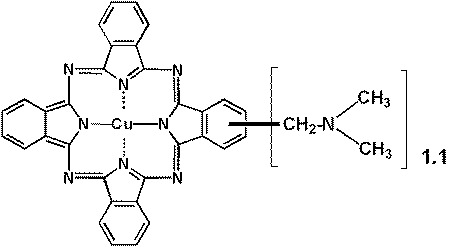
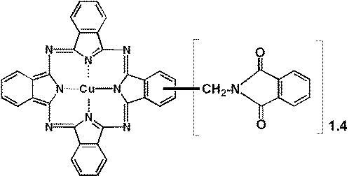


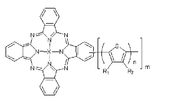
一般式(1)ないし(2)のフタロシアニン誘導体は、フタロシアニン環に側鎖もしくは官能基を導入することにより、合成することができる。 [化4]、[化5]、[化6]記載のスルホン酸化銅フタロシアニンは銅フタロシアニンを発煙硫酸(三酸化硫黄濃度:20%)中で加熱することにより得ることができ、[化9]の化合物の合成は、例えば特許文献(米国特許2761868号)に開示の方法で合成することができる。
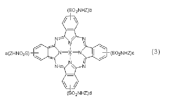


一般式(3)で表されるフタロシアニン誘導体は、フタロシアニン環が少なくとも1個以上のスルファモイル基で置換された化合物である。導入されるスルファモイル基は、フタロシアニン環1個あたり少なくとも1個であれば特に限定なく用いることができるが、好ましくは1又は2個、より好ましくは1個である。置換される位置は、特に限定はない。
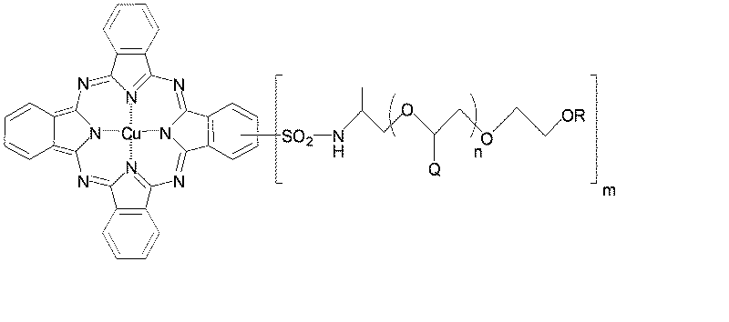

好ましいR及びR’として、低級アルキル基、特にメチル基を挙げることができ、mとしては、1~6の整数であるものが好ましい。具体的に好ましいフタロシアニン誘導体として以下が挙げられる。なお、ここで、置換基を有するフタロシアニンの式の括弧の横の数字はフタロシアニン分子に対する官能基の平均導入数を表している。個々の分子についての置換基導入数は整数であるが、実際においては置換基導入数の異なるものを混在して使用するためである。
ポリエーテルモノアミンは市販品としても提供されており、例えばJEFFAMINE Mシリーズ(商品名、米国Huntsman社製)がある。
本製造方法は、
(a)無置換フタロシアニンと置換基を有するフタロシアニン(フタロシアニン誘導体)とを酸に溶解させた後に、貧溶媒に析出させて複合体を得る工程(a)と、
(b)前記複合体を微粒子化して、微粒子化複合体を得る工程(b)と、
(c)前記微粒子化複合体を有機溶媒に分散させて分散体を得る工程(c)と、
(d)前記分散体をナノワイヤ化する工程(d)と
を有するものである。
一般にフタロシアニン類は硫酸などの酸溶媒に可溶であることが知られており、本発明のフタロシアニンナノワイヤの製造方法においても、まず前記無置換フタロシアニンと前記置換基を有するフタロシアニンとを硫酸、クロロ硫酸、メタンスルホン酸、トリフルオロ酢酸等の酸溶媒に溶解させる。その後に水などの貧溶媒に投入して該無置換フタロシアニンと該置換基を有するフタロシアニン誘導体の複合体を析出させる。
工程(b)は、前記工程(a)を経て得られた複合体を微粒子化することができれば、その方法は特に限定されるものではないが、湿式分散法で前記複合体を微粒子化することが好ましい。例えば、工程(a)で得られた複合体をビーズミル、ペイントコンディショナーなどの微小ビーズを用いた湿式分散機や、プライミクス社製のT.K.フィルミックスに代表されるメディアレス分散機を用いて、水もしくは有機溶媒及び含水有機溶媒などの分散溶媒とともに湿式分散して、該複合体を微粒子化することができる。ここで該複合体の分散溶媒に対する質量比に関しては特に制限はないが、分散効率の観点から、固形分濃度を1質量%から30質量%の範囲で分散処理することが好ましい。分散処理にジルコニアビーズなどの微小メディアを使用する場合は、該複合体の微粒子化の程度を鑑みて、そのビーズ径は0.01mmから2mmの範囲が好ましい。また微小メディアの使用量は微粒子化の効率と回収効率の観点から、該複合体の分散液に対して、100質量%から1000質量%の範囲が最も好適である。
また、工程(b)においては、前記工程(a)含水複合体を乾燥して水分を完全に除去した後、N-メチルピロリドンやジクロロベンゼンやエタノールなどの有機溶媒中で湿式分散して、微粒子化を行い、微粒子化複合体を得てもよい。
工程(c)は、工程(b)を経て得られた微粒子化複合体をN-メチルピロリドンなどの有機溶媒に分散させる。該有機溶媒に関してはフタロシアニン類との親和性が低いものでなければ特に制限はないが、例えば、フタロシアニン類との親和性が高いアミド系溶媒及び芳香族有機溶媒が好ましく、具体的には、フタロシアニンと特に親和性が高いN,N-ジメチルアセトアミド、N,N-ジメチルホルムアミド、N-メチルピロリドンやトルエン、キシレン、エチルベンゼン、クロロベンゼン、ジクロロベンゼンを最も好適な有機溶媒として挙げることができる。上記アミド系有機溶媒及び芳香族有機溶媒は単独で用いることもできるが、該アミド系有機溶媒と該芳香族有機溶媒とを任意の比率で混合して使用することもでき、さらには他の有機溶媒と併用して用いることもできる。
工程(c)を経て得られた微粒子化複合体の有機溶媒分散液を(加熱)攪拌、もしくは(加熱)静置することにより、ナノワイヤが製造できる。本工程において、温度は、5℃から250℃の範囲が好ましく、さらに好ましくは20℃から200℃である。温度が5℃以上であれば、十分にフタロシアニン類の結晶成長を誘発することができ、目的とする一方向結晶成長により、ナノワイヤへ成長可能であり、また250℃以下であればナノワイヤの凝集、融着がほとんど見られず、幅方向に結晶成長して粗大化することもない。またナノワイヤ化のための攪拌時間もしくは静置時間には特に限定はないが、フタロシアニンナノワイヤの長さが100nm以上に成長するまでに、少なくとも10分以上攪拌もしくは静置することが好ましい。
ここで、無置換フタロシアニンと置換基を有するフタロシアニンが工程(a)の晶析で複合化され、さらに工程(b)の微粒子化複合体を経て、工程(d)でナノワイヤ化する機構に関しては必ずしも明確ではないが、以下に述べるようにしてナノワイヤ化が起きているものと推測される。すなわち、工程(b)で得られる微粒子化複合体の粒子径が10nmから20nmであり、該微粒子化複合体粒子が工程(d)により、フタロシアニンの結晶面方向に連結して、一方向にのみ結晶成長することにより、ナノワイヤ化する。この際、工程(c)の有機溶媒はフタロシアニンの良分散媒として機能しており、一方向結晶成長を誘発してナノワイヤ化をより促進しているものと考えられる(推定機構1)。
本製造方法は、水溶性多価アルコール中において、置換基を有するフタロシアニンの存在下、イソインドリン化合物と金属イオンとを反応させることを特徴とするものである。
撹拌時の温度が80℃よりも高い場合は混合が不十分な段階で一部にナノレベルより大きなサイズのフタロシアニン結晶が生成したり、収率が低下したりする場合もあるため、80℃以下で行うことが好ましい。

が挙げられる。環Aがベンゼン環である場合に、その他の部位にハロゲン原子やアルキル基などの官能基が導入されているものでもよい。
また、ハロゲン系有機溶剤として、クロロホルム、塩化メチレン、又はジクロロエタン等の有機溶剤を挙げることができる。この中で、特に好ましいものはジクロロベンゼンである。
次に、本発明の光電変換素子について説明する。本発明の光電変換素子は、少なくとも一対の電極、すなわち正極と負極を有し、これら電極間に本発明の光電変換素子用材料を膜化したものを含む。図1は本発明の光電変換素子の一例を示す模式図である。図1において符号1は基板、符号2は電極a、符号3は本発明の光電変換素子用材料を含む光電変換層(有機半導体層)、符号4は電極bである。
これらバッファー層は、単層であってもよく、また、異なる材料を積層したものであってもよい。
<光電変換素子用材料の製造>
・工程(a)(晶析工程)
銅フタロシアニン(Fastogen Blue 5380E、DIC製)1.67gと置換基を有するフタロシアニンのうち、[化9]で表される誘導体0.83gを濃硫酸(関東化学製)81gに投入して完全に溶解させ、濃硫酸溶液を調製した。続いて蒸留水730gを1000mLのビーカーに投入し、これを氷水で十分、冷却した後、該蒸留水を撹拌しながら、先に調製した濃硫酸溶液を投入し、銅フタロシアニンと[化9]で表される銅フタロシアニン誘導体とからなる複合体を析出させた。
工程(a)で得られた銅フタロシアニンと[化9]で表される銅フタロシアニン誘導体からなる複合体2.5gを含む含水複合体12.4gを容量50mLのポリプロピレン製容器に投入し、さらに蒸留水を4.3g加えて、該複合体の水に対する重量比を15%とし、次いでφ0.5mmのジルコニアビーズ60gを加えて、ペイントシェイカーを用いて2時間、微分散した。続いて微粒子化した複合体をジルコニアビーズから分離回収し、これをろ過し、微粒子複合体を得た。
工程(b)で得られた微粒子化複合体をオルトジクロロベンゼン60gに分散し、2時間攪拌した後にさらに60gのN-メチルピロリドンを加えて、さらに2時間攪拌した。
工程(c)で得られた分散体を、オイルバスを用いて加熱し、90分かけて145℃まで昇温した。145℃に到達後、そのままの温度でさらに30分間加熱を継続した。
上記分散液(1)150mgとPCBM(フロンティアカーボン社製)10mgとオルトジクロロベンゼン350mgをサンプル瓶の中に加え、超音波洗浄機(47kHz)中で30分間超音波照射することにより光電変換素子用材料(1)を得た。
ガラス基板にスパッタリング法により正極となるITO透明導電層を100nm堆積させ、これをフォトリソグラフィー法により2mm幅の短冊状にパターニングした。得られたパターンITO付きガラス基板を中性洗剤、蒸留水、アセトン、エタノールの順にそれぞれにつき3回15分間超音波洗浄した後、30分間UV/オゾン処理し、この上にPEDOT:PSS水分散液(商品名AI4083、HCStarck社製)をスピンコートすることで、PEDOT:PSSよりなるバッファー層1を60nmの厚さで形成した。これをホットプレートにより100℃で5分間加熱乾燥した後、当該PEDOT:PSS層上に光電変換層用材料(1)をスピンコートし、膜厚100nmの光電変換層用材料(1)由来の有機半導体層を形成した。その後、上記「有機半導体層が形成された基板」と蒸着用メタルマスク(2mm幅の短冊パターン形成用)を真空蒸着装置内に設置して、装置内の真空度を5×10-4Paまで高めた後、抵抗加熱法によって、負極となるアルミニウムを2mm幅の短冊パターンになるように蒸着堆積した(膜厚:80nm)。以上のようにして、面積が2mm×2mm(短冊状のITO層とアルミニウム層が交差する部分)である光電変換素子(1)を作製した。
実施例1で作製された光電変換素子(1)の正極と負極をデジタルマルチメーター(商品名6241A、ADC社製)に接続して、擬似太陽光(簡易型ソーラシミュレータ XES151S、三永電機製作所製、スペクトル形状:AM1.5、強度:100mW/cm2)の照射下(ITO層側から照射)、大気中で電圧を-0.1Vから+0.8Vまで掃引し、電流値を測定した。この時の短絡電流密度(印加電圧が0Vのときの電流密度の値。以下、Jsc)は5.17mA/cm2、開放電圧(電流密度が0になるときの印加電圧の値。以下、Voc)は0.57V、フィルファクター(FF)は0.37であり、これらの値から算出した光電変換効率(PCE)は1.11%であった。なお、FFとPCEは次式により算出した。
FF=JVmax/(Jsc×Voc)
(ここで、JVmaxは、印加電圧が0Vから開放電圧値の間で電流密度と印加電圧の積が最大となる点における電流密度と印加電圧の積の値である。)
PCE=[(Jsc×Voc×FF)/擬似太陽光強度(100mW/cm2)]×100(%)
実施例(1)で得た分散液(1)180mgにオルトジクロロベンゼン180mgを加え光電変換素子用材料(2)を得た。
光電変換素子用材料(1)の変わりに光電変換素子用材料(2)を使用し実施例(1)と同様に光電変換素子用材料(2)由来の有機半導体(電子供与性材料)層を形成した後、この上に、2重量%のPCBM-オルトジクロロベンゼンをスピンコートし電子受容性材料層を積層した以外は実施例(1)と同様にして光電変換素子(2)を製造した。
光電変換素子(1)の替わりに光電変換素子(2)を用いる他は、評価例1と同様にして評価を行った結果、Jscは4.98mA/cm2、Vocは0.57V、FFは0.39であり、これらの値から算出したPCEは1.11%であった。
ポリエーテルモノアミンとして、Surfonamine B-200(商品名、第一アミン-末端ポリ(エチレンオキシド/プロピレンオキシド)(5/95)コポリマー、数平均分子量約2,000、Huntsman Corporation製)692質量部と炭酸ナトリウム66質量部と水150質量部の混合物に、銅フタロシアニンスルホニルクロリド(スルホン化度=1)210質量部を投入し、5℃~室温で6時間反応させた。得られた反応混合物を真空下で90℃に加熱して水を除去し、下記[化20]で表される銅フタロシアニンスルファモイル化合物を得た。
光電変換素子(1)の替わりに光電変換素子(3)を用いる他は、評価例1と同様にして評価を行った結果、Jscは2.41mA/cm2、Vocは0.50V、FFは0.17であり、これらの値から算出したPCEは0.21%であった。
実施例1における[化9]で表される化合物の替わりに、[化5]で表される化合物を用いる他は、実施例1と同様にして、光電変換素子材料(4)、及び光電変換素子(4)を作製した。
光電変換素子(1)の替わりに光電変換素子(4)を用いる他は、評価例1と同様にして評価を行った結果、Jscは0.83mA/cm2、Vocは0.48V、FFは0.27であり、これらの値から算出したPCEは0.11%であった。
実施例1における[化9]で表される化合物の替わりに、[化6]で表される化合物を用いる他は、実施例1と同様にして、光電変換素子材料(5)、及び光電変換素子(5)を作製した。
光電変換素子(1)の替わりに光電変換素子(5)を用いる他は、評価例1と同様にして評価を行った結果、Jscは1.56mA/cm2、Vocは0.42V、FFは0.15であり、これらの値から算出したPCEは0.10%であった。
実施例1における[化9]で表される化合物の替わりに、[化7]で表される化合物を用いる他は、実施例1と同様にして、光電変換素子材料(6)、及び光電変換素子(6)を作製した。
光電変換素子(1)の替わりに光電変換素子(6)を用いる他は、評価例1と同様にして評価を行った結果、Jscは2.33mA/cm2、Vocは0.52V、FFは0.14であり、これらの値から算出したPCEは0.16%であった。
実施例1における[化9]で表される化合物の替わりに、[化8]で表される化合物を用いる他は、実施例1と同様にして、光電変換素子材料(7)、及び光電変換素子(7)を作製した。
光電変換素子(1)の替わりに光電変換素子(7)を用いる他は、評価例1と同様にして評価を行った結果、Jscは3.49mA/cm2、Vocは0.51V、FFは0.22であり、これらの値から算出したPCEは0.40%であった。
実施例1において、PCBM(フロンティアカーボン社製)10mgの替わりに、CNPPV(ポリ(2,5-ジ(ヘキシルオキシ)-シアノテレフタリデン)(アルドリッチ製)10mgを用いる他は、実施例1と同様にして、光電変換素子材料(8)、及び光電変換素子(8)を作製した。
光電変換素子(1)の替わりに光電変換素子(8)を用いる他は、評価例1と同様にして評価を行った結果、Jscは1.46mA/cm2、Vocは0.49V、FFは0.13であり、これらの値から算出したPCEは0.10%であった。
実施例(1)で製造したフタロシアニンナノワイヤのかわりに銅フタロシアニンを用いた以外は実施例(1)と同様にして光電変換素子の製造を行なったが、銅フタロシアニンの溶剤分散性が低く、当該分散液を用いて光電変換素子層を形成することが出来なかった。
2 電極a
3 光電変換層
4 電極b
5 本発明のフタロシアニンナノワイヤを含有する層(電極aが正極の場合)、又は電子受容性材料を含有する層(電極aが負極の場合)
6 電子受容性材料を含有する層(電極bが負極の場合)、又は本発明のフタロシアニンナノワイヤを含有する層(電極bが正極の場合)
Claims (11)
- 短径が50nm以下であって、その短径に対する長さの比率(長さ/短径)が10以上であるフタロシアニンナノワイヤを含有する光電変換素子用材料。
- 前記フタロシアニンナノワイヤが、無置換フタロシアニン及び置換基を有するフタロシアニンを含有する請求項1に記載の光電変換素子用材料。
- 無置換フタロシアニンが、無置換銅フタロシアニン、無置換亜鉛フタロシアニン又は無置換鉄フタロシアニンである請求項2に記載の光電変換素子用材料。
- 置換基を有するフタロシアニンが、一般式(1)又は(2)で表される請求項2に記載の光電変換素子用材料。
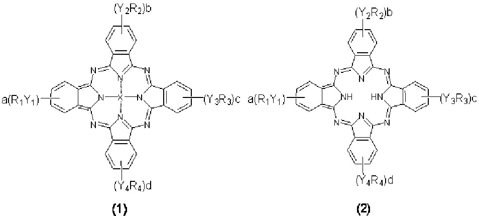
Y4は、フタロシアニン骨格とR1~R4を結合させる結合基を表し、
Y1からY4が結合基として存在しない場合には、R1~R4は、SO3H、CO2H、置換基を有してもよいアルキル基、置換基を有してもよい(オリゴ)アリール基、置換基を有してもよい(オリゴ)へテロアリール基、置換基を有してもよいフタルイミド基又は置換基を有してもよいフラーレン類であり、
Y1からY4が、-(CH2)n-(nは1~10の整数を表す)、-CH=CH-、-C≡C-、-O-、-NH-、-S-、-S(O)-、又は-S(O)2-で表される結合基である場合には、R1~R4は、置換基を有してもよいアルキル基、置換基を有してもよい(オリゴ)アリール基、置換基を有してもよい(オリゴ)へテロアリール基、置換基を有してもよいフタルイミド基又は置換基を有してもよいフラーレン類であり、a、b、c及びdは各々独立に0~4の整数を表すが、そのうち少なくとも一つは0ではない。) - 前記置換基を有してもよいアルキル基が、メチル基、エチル基又はプロピル基であり、置換基を有してもよい(オリゴ)アリール基が、置換基を有してもよい(オリゴ)フェニレン基又は置換基を有してもよい(オリゴ)ナフチレン基であり、置換基を有してもよい(オリゴ)へテロアリール基が、置換基を有してもよい(オリゴ)ピロール基、置換基を有してもよい(オリゴ)チオフェン基、置換基を有してもよい(オリゴ)ベンゾピロール基又は置換基を有してもよい(オリゴ)ベンゾチオフェン基である請求項4に記載の光電変換素子用材料。
- 置換基を有するフタロシアニンが、一般式(3)で表される請求項2に記載の光電変換素子用材料。


- 請求項1~6の何れかに記載の光電変換素子用材料が、更に電子受容性材料を含むものである光電変換素子用材料。
- 前記電子受容性材料がフラーレン類である請求項7に記載の光電変換素子用材料。
- 前記電子受容性材料が電子受容性ポリマーである請求項7に記載の光電変換素子用材料。
- 前記電子受容性材料がペリレン類である請求項7に記載の光電変換素子用材料。
- 少なくとも正極と負極を有する光電変換素子であって、正極と負極の間に請求項1~10の何れかに記載の光電変換素子用材料を含むことを特徴とする光電変換素子。
Priority Applications (5)
| Application Number | Priority Date | Filing Date | Title |
|---|---|---|---|
| CN201080034363.7A CN102484204B (zh) | 2009-11-26 | 2010-10-12 | 光电转换元件用材料及光电转换元件 |
| EP10832980.6A EP2506327A4 (en) | 2009-11-26 | 2010-10-12 | FABRIC FOR A PHOTOELECTRIC CONVERSION ELEMENT AND PHOTOELECTRIC CONVERSION ELEMENT |
| KR1020117025886A KR101417882B1 (ko) | 2009-11-26 | 2010-10-12 | 광전 변환 소자용 재료 및 광전 변환 소자 |
| JP2011504665A JP4844701B2 (ja) | 2009-11-26 | 2010-10-12 | 光電変換素子用材料及び光電変換素子 |
| US13/511,005 US8629431B2 (en) | 2009-11-26 | 2010-10-12 | Material for photoelectric conversion device and photoelectric conversion device |
Applications Claiming Priority (2)
| Application Number | Priority Date | Filing Date | Title |
|---|---|---|---|
| JP2009-268641 | 2009-11-26 | ||
| JP2009268641 | 2009-11-26 |
Publications (1)
| Publication Number | Publication Date |
|---|---|
| WO2011065133A1 true WO2011065133A1 (ja) | 2011-06-03 |
Family
ID=44066237
Family Applications (1)
| Application Number | Title | Priority Date | Filing Date |
|---|---|---|---|
| PCT/JP2010/067826 Ceased WO2011065133A1 (ja) | 2009-11-26 | 2010-10-12 | 光電変換素子用材料及び光電変換素子 |
Country Status (7)
| Country | Link |
|---|---|
| US (1) | US8629431B2 (ja) |
| EP (1) | EP2506327A4 (ja) |
| JP (1) | JP4844701B2 (ja) |
| KR (1) | KR101417882B1 (ja) |
| CN (1) | CN102484204B (ja) |
| TW (1) | TWI495690B (ja) |
| WO (1) | WO2011065133A1 (ja) |
Cited By (3)
| Publication number | Priority date | Publication date | Assignee | Title |
|---|---|---|---|---|
| CN102623640A (zh) * | 2012-04-09 | 2012-08-01 | 苏州大学 | 太阳能电池 |
| WO2013151128A1 (ja) | 2012-04-06 | 2013-10-10 | Dic株式会社 | フタロシアニンナノサイズ構造物、及び該ナノサイズ構造物を用いた電子素子 |
| US9490442B2 (en) | 2014-04-04 | 2016-11-08 | Samsung Electronics Co., Ltd. | Organic photoelectronic device and image sensor |
Families Citing this family (10)
| Publication number | Priority date | Publication date | Assignee | Title |
|---|---|---|---|---|
| CN103456508B (zh) * | 2012-05-31 | 2017-04-12 | 海洋王照明科技股份有限公司 | 一种石墨烯复合电极的制备方法 |
| WO2013183548A1 (ja) * | 2012-06-07 | 2013-12-12 | 住友化学株式会社 | 有機光電変換素子の製造方法 |
| US8993998B2 (en) * | 2012-07-02 | 2015-03-31 | The Regents Of The University Of California | Electro-optic device having nanowires interconnected into a network of nanowires |
| TWI492409B (zh) * | 2013-03-15 | 2015-07-11 | Nat Univ Dong Hwa | 太陽能電池的製造方法 |
| US8945978B2 (en) * | 2013-06-28 | 2015-02-03 | Sunpower Corporation | Formation of metal structures in solar cells |
| CN103601728B (zh) * | 2013-11-25 | 2015-09-09 | 吉林大学 | 在水或水/醇中可溶的酞菁衍生物及用于制备有机和聚合物太阳能光伏器件 |
| CN109755395B (zh) * | 2017-11-08 | 2021-07-16 | 中国科学院化学研究所 | 一种应用风刀涂布制备有机聚合物薄膜太阳能电池的方法 |
| CN110085753B (zh) * | 2019-05-05 | 2021-06-11 | 中南大学 | 一种非富勒烯钙钛矿太阳能电池及其制备方法 |
| JP7519616B2 (ja) * | 2020-01-22 | 2024-07-22 | 富士フイルムビジネスイノベーション株式会社 | 熱電変換素子、および熱電変換素子を備える物品 |
| KR20230034784A (ko) * | 2021-09-03 | 2023-03-10 | 삼성전자주식회사 | 유기 광전 변환 소자 및 이를 포함하는 이미지 센서 |
Citations (13)
| Publication number | Priority date | Publication date | Assignee | Title |
|---|---|---|---|---|
| US2761868A (en) | 1953-05-13 | 1956-09-04 | American Cyanamid Co | Sulfonated and unsulfonated imidomethyl, carboxyamidomethyl and aminomethyl phthalocyanines |
| WO2003076332A1 (en) * | 2002-03-08 | 2003-09-18 | Communications Research Laboratory, Independent Administrative Institution | Production device and production method for conductive nano-wire |
| JP2005145896A (ja) | 2003-11-17 | 2005-06-09 | Dainippon Ink & Chem Inc | 金属フタロシアニンの製造方法 |
| JP2006143680A (ja) | 2004-11-22 | 2006-06-08 | Hiroshima Univ | 新規化合物及びその製造方法並びにその利用 |
| JP2006245073A (ja) | 2005-02-28 | 2006-09-14 | Dainippon Printing Co Ltd | 有機薄膜太陽電池 |
| JP2007039561A (ja) | 2005-08-03 | 2007-02-15 | Fujifilm Holdings Corp | フタロシアニン類の製造方法 |
| JP2007519636A (ja) | 2004-01-08 | 2007-07-19 | ビーエーエスエフ アクチェンゲゼルシャフト | フタロシアニンの製造方法 |
| JP2007526881A (ja) | 2003-07-02 | 2007-09-20 | ランクセス・ドイチュランド・ゲーエムベーハー | アルコキシ置換フタロシアニンの製造方法 |
| JP2008016834A (ja) | 2006-06-09 | 2008-01-24 | Mitsubishi Chemicals Corp | 有機光電変換素子の製造方法及び有機光電変換素子 |
| JP2009509037A (ja) * | 2005-09-15 | 2009-03-05 | 本田技研工業株式会社 | 金属ナノワイヤーの合成方法 |
| JP2009135237A (ja) | 2007-11-29 | 2009-06-18 | Nagoya Institute Of Technology | 溶解性フラーレン誘導体 |
| JP2009280531A (ja) * | 2008-05-23 | 2009-12-03 | Dic Corp | 金属フタロシアニンナノワイヤー及びその製造方法 |
| WO2010122921A1 (ja) * | 2009-04-23 | 2010-10-28 | Dic株式会社 | フタロシアニンナノワイヤー、それを含有するインキ組成物及び電子素子、並びにフタロシアニンナノワイヤーの製造方法 |
Family Cites Families (12)
| Publication number | Priority date | Publication date | Assignee | Title |
|---|---|---|---|---|
| JP2002121420A (ja) * | 2000-08-07 | 2002-04-23 | Dainippon Ink & Chem Inc | 銅フタロシアニン顔料及びその製造方法 |
| JP2003071799A (ja) * | 2001-09-04 | 2003-03-12 | Mitsubishi Chemicals Corp | ナノワイヤ及びその製造方法 |
| DE20121631U1 (de) * | 2001-11-09 | 2003-06-18 | Friz Biochem GmbH, 82152 Planegg | Molekulares elektronisches Bauelement zum Aufbau nanoelektronischer Schaltungen, molekulare elektronische Baugruppe und elektronische Schaltung |
| JP5023456B2 (ja) * | 2005-03-28 | 2012-09-12 | 大日本印刷株式会社 | 有機薄膜太陽電池素子 |
| JP5023455B2 (ja) * | 2005-03-28 | 2012-09-12 | 大日本印刷株式会社 | 有機薄膜太陽電池の製造方法および有機薄膜太陽電池 |
| JP2007005864A (ja) | 2005-06-21 | 2007-01-11 | Seiko Epson Corp | 合成画像編集装置、合成画像編集方法およびコンピュータプログラム |
| JP5008048B2 (ja) * | 2005-06-27 | 2012-08-22 | 独立行政法人情報通信研究機構 | 導電性ナノワイヤーを用いたトランジスタ |
| US7942938B2 (en) * | 2005-07-08 | 2011-05-17 | Basf Se | Gas-resistant phtalocyanine dyes |
| CA2650991C (en) | 2006-05-01 | 2015-02-17 | David Loren Carroll | Organic optoelectronic devices and applications thereof |
| KR101312269B1 (ko) | 2007-01-05 | 2013-09-25 | 삼성전자주식회사 | 고분자 태양전지 및 그의 제조방법 |
| US20080202581A1 (en) * | 2007-02-12 | 2008-08-28 | Solasta, Inc. | Photovoltaic cell with reduced hot-carrier cooling |
| JP2008266382A (ja) * | 2007-04-17 | 2008-11-06 | Fujifilm Corp | フタロシアニン顔料ナノ粒子分散物の製造方法、及びその分散物を含有するカラーフィルタ用インクジェットインクの製造方法、並びにその分散物を含有する着色感光性樹脂組成物、感光性転写材料、及びカラーフィルタ、それらを用いた液晶表示装置及びccdデバイス |
-
2010
- 2010-10-12 US US13/511,005 patent/US8629431B2/en not_active Expired - Fee Related
- 2010-10-12 JP JP2011504665A patent/JP4844701B2/ja not_active Expired - Fee Related
- 2010-10-12 CN CN201080034363.7A patent/CN102484204B/zh not_active Expired - Fee Related
- 2010-10-12 KR KR1020117025886A patent/KR101417882B1/ko not_active Expired - Fee Related
- 2010-10-12 WO PCT/JP2010/067826 patent/WO2011065133A1/ja not_active Ceased
- 2010-10-12 EP EP10832980.6A patent/EP2506327A4/en not_active Withdrawn
- 2010-10-22 TW TW099136023A patent/TWI495690B/zh not_active IP Right Cessation
Patent Citations (13)
| Publication number | Priority date | Publication date | Assignee | Title |
|---|---|---|---|---|
| US2761868A (en) | 1953-05-13 | 1956-09-04 | American Cyanamid Co | Sulfonated and unsulfonated imidomethyl, carboxyamidomethyl and aminomethyl phthalocyanines |
| WO2003076332A1 (en) * | 2002-03-08 | 2003-09-18 | Communications Research Laboratory, Independent Administrative Institution | Production device and production method for conductive nano-wire |
| JP2007526881A (ja) | 2003-07-02 | 2007-09-20 | ランクセス・ドイチュランド・ゲーエムベーハー | アルコキシ置換フタロシアニンの製造方法 |
| JP2005145896A (ja) | 2003-11-17 | 2005-06-09 | Dainippon Ink & Chem Inc | 金属フタロシアニンの製造方法 |
| JP2007519636A (ja) | 2004-01-08 | 2007-07-19 | ビーエーエスエフ アクチェンゲゼルシャフト | フタロシアニンの製造方法 |
| JP2006143680A (ja) | 2004-11-22 | 2006-06-08 | Hiroshima Univ | 新規化合物及びその製造方法並びにその利用 |
| JP2006245073A (ja) | 2005-02-28 | 2006-09-14 | Dainippon Printing Co Ltd | 有機薄膜太陽電池 |
| JP2007039561A (ja) | 2005-08-03 | 2007-02-15 | Fujifilm Holdings Corp | フタロシアニン類の製造方法 |
| JP2009509037A (ja) * | 2005-09-15 | 2009-03-05 | 本田技研工業株式会社 | 金属ナノワイヤーの合成方法 |
| JP2008016834A (ja) | 2006-06-09 | 2008-01-24 | Mitsubishi Chemicals Corp | 有機光電変換素子の製造方法及び有機光電変換素子 |
| JP2009135237A (ja) | 2007-11-29 | 2009-06-18 | Nagoya Institute Of Technology | 溶解性フラーレン誘導体 |
| JP2009280531A (ja) * | 2008-05-23 | 2009-12-03 | Dic Corp | 金属フタロシアニンナノワイヤー及びその製造方法 |
| WO2010122921A1 (ja) * | 2009-04-23 | 2010-10-28 | Dic株式会社 | フタロシアニンナノワイヤー、それを含有するインキ組成物及び電子素子、並びにフタロシアニンナノワイヤーの製造方法 |
Non-Patent Citations (6)
| Title |
|---|
| CHEMICAL COMMUNICATIONS, 2003, pages 2062 |
| H. XIN ET AL.: "Bulk Heterojunction Solar Cells from Poly(3-butylthiophene)/Fullerene Blends: In Situ Self-Assembly of Nanowires, Morphology, Charge Transport, and Photovoltaic Properties", CHEMISTRY OF MATERIALS, vol. 20, no. 19, 14 October 2008 (2008-10-14), pages 6199 - 6207, XP008157158 * |
| JOURNAL OF MATERIALS CHEMISTRY, vol. 18, 2008, pages 1984 |
| See also references of EP2506327A4 |
| SYNTHESIS, 1981, pages 1 |
| W. Y. TONG ET AL.: "Synthesis and properties of copper phthalocyanine nanowires", THIN SOLID FILMS, vol. 515, no. 13, 7 May 2007 (2007-05-07), pages 5270 - 5274, XP022015264 * |
Cited By (8)
| Publication number | Priority date | Publication date | Assignee | Title |
|---|---|---|---|---|
| WO2013151128A1 (ja) | 2012-04-06 | 2013-10-10 | Dic株式会社 | フタロシアニンナノサイズ構造物、及び該ナノサイズ構造物を用いた電子素子 |
| JP2013216603A (ja) * | 2012-04-06 | 2013-10-24 | Dic Corp | フタロシアニンナノサイズ構造物、及び該ナノサイズ構造物を用いた電子素子 |
| KR20140105540A (ko) | 2012-04-06 | 2014-09-01 | 디아이씨 가부시끼가이샤 | 프탈로시아닌 나노사이즈 구조물, 및 당해 나노사이즈 구조물을 사용한 전자 소자 |
| CN104169285A (zh) * | 2012-04-06 | 2014-11-26 | Dic株式会社 | 酞菁纳米尺寸结构物、和使用该纳米尺寸结构物的电子元件 |
| US9324956B2 (en) | 2012-04-06 | 2016-04-26 | Dic Corporation | Phthalocyanine nano-size structures, and electronic elements using said nano-size structures |
| CN104169285B (zh) * | 2012-04-06 | 2016-10-26 | Dic株式会社 | 酞菁纳米尺寸结构物、和使用该纳米尺寸结构物的电子元件 |
| CN102623640A (zh) * | 2012-04-09 | 2012-08-01 | 苏州大学 | 太阳能电池 |
| US9490442B2 (en) | 2014-04-04 | 2016-11-08 | Samsung Electronics Co., Ltd. | Organic photoelectronic device and image sensor |
Also Published As
| Publication number | Publication date |
|---|---|
| JP4844701B2 (ja) | 2011-12-28 |
| KR20120023629A (ko) | 2012-03-13 |
| EP2506327A1 (en) | 2012-10-03 |
| EP2506327A4 (en) | 2014-04-16 |
| CN102484204A (zh) | 2012-05-30 |
| KR101417882B1 (ko) | 2014-07-09 |
| TWI495690B (zh) | 2015-08-11 |
| TW201118136A (en) | 2011-06-01 |
| JPWO2011065133A1 (ja) | 2013-04-11 |
| CN102484204B (zh) | 2015-05-20 |
| US8629431B2 (en) | 2014-01-14 |
| US20120308822A1 (en) | 2012-12-06 |
Similar Documents
| Publication | Publication Date | Title |
|---|---|---|
| JP4844701B2 (ja) | 光電変換素子用材料及び光電変換素子 | |
| JP4998645B1 (ja) | フタロシアニンナノロッド、及び光電変換素子 | |
| JP5338939B2 (ja) | フタロシアニンナノサイズ構造物、及び該ナノサイズ構造物を用いた電子素子 | |
| Meng et al. | Three-bladed rylene propellers with three-dimensional network assembly for organic electronics | |
| Duan et al. | Recent advances in water/alcohol-soluble π-conjugated materials: new materials and growing applications in solar cells | |
| Li et al. | Polymer–metal-oxide hybrid solar cells | |
| KR101195078B1 (ko) | 프탈로시아닌 나노 와이어, 그것을 함유하는 잉크 조성물 및 전자 소자, 및 프탈로시아닌 나노 와이어의 제조 방법 | |
| KR102107532B1 (ko) | 그래핀을 전도성 투명전극으로 사용하는 페로브스카이트 기반 태양전지 | |
| JP2013254912A (ja) | 有機光電変換素子およびこれを用いた太陽電池 | |
| TWI413662B (zh) | 酞青素奈米棒及光電轉換元件 | |
| JP4666115B1 (ja) | フタロシアニンナノワイヤー、それを含有するインキ組成物及び電子素子、並びにフタロシアニンナノワイヤーの製造方法 | |
| JP2008147544A (ja) | 光起電力素子用材料および光起電力素子 | |
| JP5858272B2 (ja) | フタロシアニンナノワイヤーの製造方法 | |
| JP2012097079A (ja) | フタロシアニンナノサイズ構造物集合体の製造方法、及び該フタロシアニンナノサイズ構造物集合体を用いた電子デバイス | |
| WO2013008889A1 (ja) | 光電変換素子用材料、光電変換素子の製造方法及び光電変換素子 |
Legal Events
| Date | Code | Title | Description |
|---|---|---|---|
| WWE | Wipo information: entry into national phase |
Ref document number: 201080034363.7 Country of ref document: CN |
|
| ENP | Entry into the national phase |
Ref document number: 2011504665 Country of ref document: JP Kind code of ref document: A |
|
| 121 | Ep: the epo has been informed by wipo that ep was designated in this application |
Ref document number: 10832980 Country of ref document: EP Kind code of ref document: A1 |
|
| ENP | Entry into the national phase |
Ref document number: 20117025886 Country of ref document: KR Kind code of ref document: A |
|
| WWE | Wipo information: entry into national phase |
Ref document number: 2010832980 Country of ref document: EP |
|
| NENP | Non-entry into the national phase |
Ref country code: DE |
|
| WWE | Wipo information: entry into national phase |
Ref document number: 13511005 Country of ref document: US |