WO2011065014A1 - 光導波路デバイスおよびモジュール - Google Patents
光導波路デバイスおよびモジュール Download PDFInfo
- Publication number
- WO2011065014A1 WO2011065014A1 PCT/JP2010/006913 JP2010006913W WO2011065014A1 WO 2011065014 A1 WO2011065014 A1 WO 2011065014A1 JP 2010006913 W JP2010006913 W JP 2010006913W WO 2011065014 A1 WO2011065014 A1 WO 2011065014A1
- Authority
- WO
- WIPO (PCT)
- Prior art keywords
- waveguide
- optical
- light
- termination structure
- shielding material
- Prior art date
- Legal status (The legal status is an assumption and is not a legal conclusion. Google has not performed a legal analysis and makes no representation as to the accuracy of the status listed.)
- Ceased
Links
Images




















Classifications
-
- G—PHYSICS
- G02—OPTICS
- G02B—OPTICAL ELEMENTS, SYSTEMS OR APPARATUS
- G02B6/00—Light guides; Structural details of arrangements comprising light guides and other optical elements, e.g. couplings
- G02B6/24—Coupling light guides
- G02B6/241—Light guide terminations
- G02B6/243—Light guide terminations as light absorbers
-
- G—PHYSICS
- G02—OPTICS
- G02B—OPTICAL ELEMENTS, SYSTEMS OR APPARATUS
- G02B6/00—Light guides; Structural details of arrangements comprising light guides and other optical elements, e.g. couplings
- G02B6/10—Light guides; Structural details of arrangements comprising light guides and other optical elements, e.g. couplings of the optical waveguide type
- G02B6/12—Light guides; Structural details of arrangements comprising light guides and other optical elements, e.g. couplings of the optical waveguide type of the integrated circuit kind
- G02B6/12007—Light guides; Structural details of arrangements comprising light guides and other optical elements, e.g. couplings of the optical waveguide type of the integrated circuit kind forming wavelength selective elements, e.g. multiplexer, demultiplexer
- G02B6/12009—Light guides; Structural details of arrangements comprising light guides and other optical elements, e.g. couplings of the optical waveguide type of the integrated circuit kind forming wavelength selective elements, e.g. multiplexer, demultiplexer comprising arrayed waveguide grating [AWG] devices, i.e. with a phased array of waveguides
- G02B6/12019—Light guides; Structural details of arrangements comprising light guides and other optical elements, e.g. couplings of the optical waveguide type of the integrated circuit kind forming wavelength selective elements, e.g. multiplexer, demultiplexer comprising arrayed waveguide grating [AWG] devices, i.e. with a phased array of waveguides characterised by the optical interconnection to or from the AWG devices, e.g. integration or coupling with lasers or photodiodes
-
- G—PHYSICS
- G02—OPTICS
- G02B—OPTICAL ELEMENTS, SYSTEMS OR APPARATUS
- G02B6/00—Light guides; Structural details of arrangements comprising light guides and other optical elements, e.g. couplings
- G02B6/24—Coupling light guides
- G02B6/26—Optical coupling means
- G02B6/30—Optical coupling means for use between fibre and thin-film device
-
- G—PHYSICS
- G02—OPTICS
- G02B—OPTICAL ELEMENTS, SYSTEMS OR APPARATUS
- G02B6/00—Light guides; Structural details of arrangements comprising light guides and other optical elements, e.g. couplings
- G02B6/10—Light guides; Structural details of arrangements comprising light guides and other optical elements, e.g. couplings of the optical waveguide type
- G02B6/12—Light guides; Structural details of arrangements comprising light guides and other optical elements, e.g. couplings of the optical waveguide type of the integrated circuit kind
-
- G—PHYSICS
- G02—OPTICS
- G02B—OPTICAL ELEMENTS, SYSTEMS OR APPARATUS
- G02B6/00—Light guides; Structural details of arrangements comprising light guides and other optical elements, e.g. couplings
- G02B6/10—Light guides; Structural details of arrangements comprising light guides and other optical elements, e.g. couplings of the optical waveguide type
- G02B6/12—Light guides; Structural details of arrangements comprising light guides and other optical elements, e.g. couplings of the optical waveguide type of the integrated circuit kind
- G02B6/12007—Light guides; Structural details of arrangements comprising light guides and other optical elements, e.g. couplings of the optical waveguide type of the integrated circuit kind forming wavelength selective elements, e.g. multiplexer, demultiplexer
- G02B6/12009—Light guides; Structural details of arrangements comprising light guides and other optical elements, e.g. couplings of the optical waveguide type of the integrated circuit kind forming wavelength selective elements, e.g. multiplexer, demultiplexer comprising arrayed waveguide grating [AWG] devices, i.e. with a phased array of waveguides
- G02B6/12016—Light guides; Structural details of arrangements comprising light guides and other optical elements, e.g. couplings of the optical waveguide type of the integrated circuit kind forming wavelength selective elements, e.g. multiplexer, demultiplexer comprising arrayed waveguide grating [AWG] devices, i.e. with a phased array of waveguides characterised by the input or output waveguides, e.g. tapered waveguide ends, coupled together pairs of output waveguides
-
- G—PHYSICS
- G02—OPTICS
- G02B—OPTICAL ELEMENTS, SYSTEMS OR APPARATUS
- G02B6/00—Light guides; Structural details of arrangements comprising light guides and other optical elements, e.g. couplings
- G02B6/10—Light guides; Structural details of arrangements comprising light guides and other optical elements, e.g. couplings of the optical waveguide type
- G02B6/12—Light guides; Structural details of arrangements comprising light guides and other optical elements, e.g. couplings of the optical waveguide type of the integrated circuit kind
- G02B6/122—Basic optical elements, e.g. light-guiding paths
- G02B6/1228—Tapered waveguides, e.g. integrated spot-size transformers
-
- G—PHYSICS
- G02—OPTICS
- G02B—OPTICAL ELEMENTS, SYSTEMS OR APPARATUS
- G02B6/00—Light guides; Structural details of arrangements comprising light guides and other optical elements, e.g. couplings
- G02B6/10—Light guides; Structural details of arrangements comprising light guides and other optical elements, e.g. couplings of the optical waveguide type
- G02B6/12—Light guides; Structural details of arrangements comprising light guides and other optical elements, e.g. couplings of the optical waveguide type of the integrated circuit kind
- G02B6/122—Basic optical elements, e.g. light-guiding paths
- G02B6/124—Geodesic lenses or integrated gratings
-
- G—PHYSICS
- G02—OPTICS
- G02B—OPTICAL ELEMENTS, SYSTEMS OR APPARATUS
- G02B6/00—Light guides; Structural details of arrangements comprising light guides and other optical elements, e.g. couplings
- G02B6/24—Coupling light guides
- G02B6/255—Splicing of light guides, e.g. by fusion or bonding
- G02B6/2552—Splicing of light guides, e.g. by fusion or bonding reshaping or reforming of light guides for coupling using thermal heating, e.g. tapering, forming of a lens on light guide ends
-
- G—PHYSICS
- G02—OPTICS
- G02B—OPTICAL ELEMENTS, SYSTEMS OR APPARATUS
- G02B6/00—Light guides; Structural details of arrangements comprising light guides and other optical elements, e.g. couplings
- G02B6/10—Light guides; Structural details of arrangements comprising light guides and other optical elements, e.g. couplings of the optical waveguide type
- G02B6/12—Light guides; Structural details of arrangements comprising light guides and other optical elements, e.g. couplings of the optical waveguide type of the integrated circuit kind
- G02B2006/12083—Constructional arrangements
- G02B2006/12126—Light absorber
-
- G—PHYSICS
- G02—OPTICS
- G02B—OPTICAL ELEMENTS, SYSTEMS OR APPARATUS
- G02B6/00—Light guides; Structural details of arrangements comprising light guides and other optical elements, e.g. couplings
- G02B6/10—Light guides; Structural details of arrangements comprising light guides and other optical elements, e.g. couplings of the optical waveguide type
- G02B6/12—Light guides; Structural details of arrangements comprising light guides and other optical elements, e.g. couplings of the optical waveguide type of the integrated circuit kind
- G02B2006/12133—Functions
- G02B2006/12142—Modulator
-
- G—PHYSICS
- G02—OPTICS
- G02B—OPTICAL ELEMENTS, SYSTEMS OR APPARATUS
- G02B6/00—Light guides; Structural details of arrangements comprising light guides and other optical elements, e.g. couplings
- G02B6/10—Light guides; Structural details of arrangements comprising light guides and other optical elements, e.g. couplings of the optical waveguide type
- G02B6/12—Light guides; Structural details of arrangements comprising light guides and other optical elements, e.g. couplings of the optical waveguide type of the integrated circuit kind
- G02B2006/12133—Functions
- G02B2006/12145—Switch
-
- G—PHYSICS
- G02—OPTICS
- G02B—OPTICAL ELEMENTS, SYSTEMS OR APPARATUS
- G02B6/00—Light guides; Structural details of arrangements comprising light guides and other optical elements, e.g. couplings
- G02B6/10—Light guides; Structural details of arrangements comprising light guides and other optical elements, e.g. couplings of the optical waveguide type
- G02B6/12—Light guides; Structural details of arrangements comprising light guides and other optical elements, e.g. couplings of the optical waveguide type of the integrated circuit kind
- G02B2006/12133—Functions
- G02B2006/1215—Splitter
-
- G—PHYSICS
- G02—OPTICS
- G02B—OPTICAL ELEMENTS, SYSTEMS OR APPARATUS
- G02B6/00—Light guides; Structural details of arrangements comprising light guides and other optical elements, e.g. couplings
- G02B6/10—Light guides; Structural details of arrangements comprising light guides and other optical elements, e.g. couplings of the optical waveguide type
- G02B6/12—Light guides; Structural details of arrangements comprising light guides and other optical elements, e.g. couplings of the optical waveguide type of the integrated circuit kind
- G02B2006/12166—Manufacturing methods
- G02B2006/12195—Tapering
-
- G—PHYSICS
- G02—OPTICS
- G02B—OPTICAL ELEMENTS, SYSTEMS OR APPARATUS
- G02B6/00—Light guides; Structural details of arrangements comprising light guides and other optical elements, e.g. couplings
- G02B6/24—Coupling light guides
- G02B6/26—Optical coupling means
- G02B6/30—Optical coupling means for use between fibre and thin-film device
- G02B6/305—Optical coupling means for use between fibre and thin-film device and having an integrated mode-size expanding section, e.g. tapered waveguide
Definitions
- the present invention relates to an optical device using a waveguide on a substrate. More specifically, the present invention relates to a technique for terminating a waveguide not connected to an input or output fiber at an arbitrary position in a substrate and attenuating the intensity of an optical signal propagating through the waveguide.
- a waveguide type device As a component that has played an important role in this optical communication system, there is a waveguide type device.
- various functions such as an optical signal branching coupler, a wavelength multiplexer / demultiplexer, an interleave filter, an optical switch, and a variable optical attenuator (VOA) have been realized. Since these devices are of the waveguide type, the circuit design is flexible, and large scale and high integration are easy.
- a semiconductor component manufacturing process such as LSI can be used, it is highly expected as a device with excellent mass productivity.
- Various types of semiconductors, waveguides using polymer materials, etc. have been put into practical use. Especially, silica-based optical waveguides fabricated on silicon substrates have low loss, stability and bondability to optical fibers. It is one of the waveguide-type devices that have the characteristics of being excellent and are most practically used.
- optical add / drop multiplexing using wavelength division multiplexing (WDM) signals
- ROADM Reconfigurable Add / Drop Multiplexing
- This system has a function to transmit all signals to adjacent nodes after passing only an arbitrary WDM channel signal within a node to a lower layer network, and mainly forms a ring network. Used.
- Optical devices required to realize this function include wavelength multiplexing / demultiplexing filters that combine and branch WDM signals for each wavelength, optical switches that switch signal paths, and signal light intensity adjustments.
- VOAs, optical transceivers, light intensity monitors, etc., in particular, wavelength multiplexing / demultiplexing filters, optical switches, VOAs and the like can be realized by waveguide devices.
- FIG. 18 shows an example of this, including wavelength multiplexing / demultiplexing filters (1404, 1406, 1416), optical switches (1408-1 to N), VOAs (1410-1 to N), and optical couplers (1402, 1412-1 to N) is a block diagram of a circuit in which monitoring PDs (Photo Detectors) (1414-1 to N) are integrated as one module 1400.
- monitoring PDs Photo Detectors
- a drop path wavelength demultiplexing (DEMUX) filter 1404 After that, one of them is separated into individual wavelength signals by a drop path wavelength demultiplexing (DEMUX) filter 1404, and only the signals of the wavelengths used in the lower layer network are detected. The other is separated into signals of individual wavelengths by another DEMUX filter 1406, and then selects either an add (Add) path signal or a main path signal that is a transmission signal from the lower layer network. Passes through the optical switches 1408-1 to 1408-1. In the 2 ⁇ 1 optical switch, a signal from the add path is selected only for the wavelength corresponding to the wavelength signal detected in the drop path.
- DEMUX drop path wavelength demultiplexing
- the signal level of each wavelength signal is adjusted by the VOAs 1410-1 to N, but the output of the signals is output by the tapping optical couplers 1412-1 to N and the monitor PDs 1414-1 to N connected thereto. A part is monitored and fed back to control the amount of attenuation of the VOA.
- the level-adjusted signal of each wavelength is converted to a WDM signal by a wavelength multiplexing (MUX) filter 1416 and then output from the output (out) of the main path.
- MUX wavelength multiplexing
- these individual optical devices have been mounted on the module by being connected to each other via an optical fiber in the module.
- further improvement in the degree of integration is a major issue.
- multi-chip integration technology This is a technique for realizing miniaturization of the waveguide device itself and reduction of the mounting area in the module by directly connecting the individual waveguide device substrates without using an optical fiber.
- the wavelength multiplexing / demultiplexing filters 1406 and 1416 are fabricated as one waveguide type device substrate 1420.
- the optical switches 1408-1 to N, the VOAs 1410-1 to N, and the optical couplers 1412-1 to N are manufactured as one waveguide type device substrate 1430. Then, when connecting each, a board
- the monitoring PDs 1414-1 to N are not waveguide devices, any one of the monitor port of the optical couplers 1412-1 to N and the end surface of the wavelength multiplexing / demultiplexing filter substrate 1420 or the end surface of the substrate 1430 such as an optical switch. In this case, it is possible to connect without using an optical fiber. According to the present technology, the length of the optical fiber used in the module 1400 and the number of members for connecting the optical fiber and the substrates 1420 and 1430 can be reduced. As a result, the mounting area in the module is reduced, Device integration is improved. At this time, the VOA has a function of adjusting the optical level of the signal light passing therethrough by an attenuation operation and suppressing the level deviation between the channels.
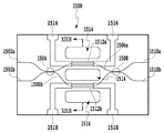
- the VOA 1500 includes two directional couplers 1504 and 1508 for branching and joining optical signals, and arm waveguides 1506a and 1506b, and a Mach-Zehnder in which thin film heaters 1512a and 1512b are formed on the arm waveguides 1506a and 1506b. It is an optical device of the interferometer (MZI: Mach Zehnder Interferometer) type.
- MZI Mach Zehnder Interferometer
- FIG. 19B is a cross-sectional view taken along line XIXB-XIXB in FIG. 19A.
- the optical waveguide is manufactured on a silicon substrate 1520, and includes a clad 1522 made of quartz glass and a rectangular core 1524 covered therewith.
- On both sides of the arm waveguide there is a heat insulating groove 1514 in which the clad is removed along the waveguide using an etching technique, and the power required for switching or attenuation can be reduced.
- the path from the port 1502a to the port 1510b is used to obtain a sufficient extinction ratio or optical attenuation even when the optical branching coupler has an error in the coupling rate due to the manufacturing error due to the interference principle of MZI.
- a route (cross route) from the port 1502b to the port 1510a is generally used as the main signal route.
- the optical attenuating operation in the VOA using MZI composed of two optical waveguides as a basic element attenuates the optical level of the main port (output waveguide connected to an optical fiber or other waveguide type device)
- the surplus (attenuated) optical power is output to the other port (dummy port).
- the port 1510b is a main port
- the port 1510a is a dummy port.
- the surplus optical power guided to the dummy port propagates to the output end face of the waveguide type device substrate and is radiated as it is to the air.
- a waveguide type device substrate 1608 such as an arrayed waveguide grating (AWG) or a monitor PD is directly attached to a waveguide type device substrate 1606 including a VOA 1602 and a tapping optical coupler 1604.
- AWG arrayed waveguide grating
- monitor PD monitor PD
- the present invention is directed to the suppression of crosstalk with respect to an optical fiber and other waveguide devices by terminating the waveguide device without radiating excess optical power at an arbitrary position on the substrate.
- a waveguide type device includes a termination structure filled with a light shielding material to terminate light from an end portion of the waveguide, and the termination structure includes: The angle of incidence with respect to the light from the waveguide end portion is inclined, the waveguide end portion has a taper portion whose waveguide width becomes narrower toward the termination, and the termination structure is formed of the waveguide. An interval between the termination structures on a surface that surrounds the end and is adjacent to or in contact with the tapered portion and faces the end of the waveguide end is greater than the interval between the termination structures at the end of the waveguide end. It is characterized by being enlarged.
- the waveguide type device is characterized in that the taper portion has an adiabatic transition structure.
- a waveguide type device includes a termination structure filled with a light shielding material to terminate light from the waveguide end, and the termination structure is connected to the waveguide end.
- the angle of incidence with respect to light is inclined, and the waveguide end has a tapered portion whose waveguide width becomes narrower toward the termination, and the termination structure surrounds the waveguide end, and the tapered portion
- the taper portion is an adiabatic transition structure.
- the waveguide type device is characterized in that the incident angle is equal to or greater than the Brewster angle.
- the waveguide type device is characterized in that the light shielding material is made of a material that absorbs or scatters light from the end of the waveguide.
- a waveguide device includes at least one of a Mach-Zehnder type optical switch, a variable attenuator, an optical splitter, and an arrayed waveguide diffraction grating.
- the module according to the embodiment of the present invention is characterized in that multi-chip integration is performed using these waveguide devices.
- a material that forms a groove on the optical waveguide by removing the clad and the core at an arbitrary position on the substrate and attenuates the light intensity in the groove.
- a material that forms a groove on the optical waveguide by removing the clad and the core at an arbitrary position on the substrate and attenuates the light intensity in the groove.
- FIG. 1 is a diagram showing a configuration of a waveguide type device according to a first embodiment of the present invention.
- 2A is a diagram showing a circuit layout of a substrate including a variable optical attenuator in the waveguide type device of FIG.
- 2B is a diagram showing a circuit layout of a substrate including a variable optical attenuator in the waveguide type device of FIG.
- FIG. 2C is a diagram showing a circuit layout of a substrate including a variable optical attenuator in the waveguide type device of FIG.
- FIG. 3 is a view showing the shape of the groove for terminating the optical waveguide according to the first embodiment of the present invention in the horizontal plane of the substrate.
- FIG. 4 is a diagram showing the shape of the groove that terminates the optical waveguide according to the fourth embodiment of the present invention in the horizontal plane of the substrate.
- FIG. 5A is a diagram illustrating a tapered shape of a terminated optical waveguide according to a fifth embodiment of the present invention.
- FIG. 5B is a diagram illustrating a tapered shape of a terminated optical waveguide according to a fifth embodiment of the present invention.
- FIG. 6 is a diagram illustrating an MMI shape of a terminated optical waveguide according to a fifth embodiment of the present invention.
- FIG. 7A is a diagram illustrating a termination structure surrounding an optical waveguide according to a sixth embodiment of the present invention.
- FIG. 7B is a diagram illustrating a termination structure surrounding an optical waveguide according to a sixth embodiment of the present invention.
- FIG. 8A is a diagram illustrating a termination structure surrounding an optical waveguide according to a seventh embodiment of the present invention.
- FIG. 8B is a diagram illustrating a termination structure surrounding an optical waveguide according to a seventh embodiment of the present invention.
- FIG. 9A is a view for explaining an optical waveguide termination structure according to an eighth embodiment of the present invention.
- FIG. 9B is a view for explaining a termination structure of an optical waveguide according to an eighth embodiment of the present invention.
- FIG. 10A is a diagram illustrating a termination structure of an optical waveguide according to an eighth embodiment of the present invention.
- FIG. 10B is a diagram illustrating a termination structure of an optical waveguide according to an eighth embodiment of the present invention.
- FIG. 11A is a diagram illustrating a tapered structure of an optical waveguide according to a ninth embodiment of the present invention.
- FIG. 11B is a diagram illustrating a tapered structure of an optical waveguide according to a ninth embodiment of the present invention.
- FIG. 12A is a diagram showing an example of a termination structure surrounding an optical waveguide according to the eighth and ninth embodiments of the present invention.
- FIG. 12B is a diagram showing an example of a termination structure surrounding the optical waveguide according to the eighth and ninth embodiments of the present invention.
- FIG. 13A is a diagram showing an outline of a waveguide type device according to a tenth embodiment of the present invention.
- FIG. 13B is a diagram showing an outline of a waveguide type device according to the tenth embodiment of the present invention.
- FIG. 14A is a diagram illustrating a specific configuration example when a 2 ⁇ 1 optical switch is realized by a waveguide device.
- FIG. 14B is a diagram illustrating a specific configuration example when a 2 ⁇ 1 optical switch is realized by a waveguide device.
- FIG. 14C is a diagram illustrating a specific configuration example in the case where the 2 ⁇ 1 optical switch is realized by a waveguide device.
- FIG. 15 is a diagram showing an outline of a waveguide type device according to the eleventh embodiment of the present invention.
- FIG. 16 is a diagram illustrating a configuration example of a 1 ⁇ 6 splitter according to a twelfth embodiment of the present invention.
- FIG. 17A is a diagram illustrating a configuration example of a 1 ⁇ 40 wavelength group demultiplexing filter according to a twelfth embodiment of the present invention.
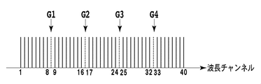
- FIG. 17B is a diagram showing an example of a transmission spectrum of the 1 ⁇ 40 wavelength group demultiplexing filter according to the twelfth embodiment of the present invention.
- FIG. 18 is a circuit block diagram showing a module configuration example of a waveguide device that realizes the main functions of the ROADM system.
- FIG. 19A is a diagram showing a basic configuration of a variable optical attenuator in a waveguide type device.
- FIG. 19A is a diagram showing a basic configuration of a variable optical attenuator in a waveguide type device.
- FIG. 19B is a cross-sectional view taken along line XIXB-XIXB in FIG. 19A.
- FIG. 20 is a diagram for explaining a problem of surplus optical power in a waveguide type device using a multi-chip integration technique according to a conventional technique.
- FIG. 1 is a diagram showing a configuration of a waveguide type device according to an embodiment of the present invention.
- the device 100 includes a substrate 120 including VOAs 104-1 to N and a substrate 130 including an arrayed waveguide grating (AWG) 110, and has an optical level adjustment function. It is comprised as a wavelength multiplexing device (VMUX: VOAequipped MUX).
- VMUX wavelength multiplexing device
- This device is installed in a WDM system, for example.
- the VOAs 104-1 to N and the tap optical couplers 106-1 to N are integrated in one substrate 120, and the optical power monitoring PD 108 and the AWG 110 are integrated in another substrate 130. .
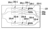
- FIG. 2A is a detailed circuit layout of the substrate 120 including the VOAs 104-1 to N in this embodiment.
- the VOAs 104-1 to N arranged in parallel are configured by MZIs 202-1 to N and 204-1 to N connected in series in two stages so that the optical levels of a plurality of channels can be adjusted simultaneously, and power is supplied to both MZIs. Attenuation operation is performed by applying.
- a wavelength-independent coupler (WINC: Wavelength Independent Coupler) is connected to the subsequent stage of the VOAs 104-1 to N as tap optical couplers 106-1 to 106-N.
- the main port 206a and the tap port 206b are connected to the AWG 110 integrated on the separate substrate 130 and the PD 108 that monitors the optical power level of each channel.
- the excess light guided from the MZIs 202-1 to N and 204-1 to N to the dummy ports 208-1 to N by the attenuation operation of the VOAs 104-1 to N is arbitrary on the extension line of the dummy port.
- the groove is formed by removing the clad layer and the core portion at the position of, and the termination structure 210-1 to 210-N composed of a material (light-shielding material) that attenuates the light intensity filled therein, and the like.
- the circuit and channel are attenuated to a level that does not cause crosstalk or stray light and terminated.
- the light shielding material in this example was a mixture of silicone resin as a base material and carbon black generally used as a light shielding material.
- the light power incident on the light shielding material is attenuated mainly by absorption in carbon black.
- the substrate 120 including these VOAs 104-1 to N is manufactured by a process as described below.
- a single-mode optical waveguide having a cladding layer and a buried core formed of quartz glass on a 6-inch diameter silicon substrate is converted into a quartz system using a flame hydrolysis reaction of a source gas such as SiCl 4 or GeCl 4. It is fabricated by a combination of glass film deposition technology and reactive ion etching technology. Then, a thin film heater and a power feeding electrode were produced on the surface of the clad layer by vacuum deposition and patterning.
- the normal core size of the manufactured optical waveguide was 7 ⁇ m ⁇ 7 ⁇ m, and the relative refractive index difference ⁇ with the cladding layer was 0.75%.
- VOA and WINC in Example 1 are formed by using such an optical waveguide and combining a straight waveguide and a curved waveguide.
- the thin film heater formed on the surface of the clad layer as a phase shifter by the thermo-optic effect had a thickness of 0.1 ⁇ m, a width of 20 ⁇ m, and a length of 2 mm.
- a heat insulating groove is formed along the thin film heater, and the heat generated from the thin film heater is efficiently transmitted to the core of the optical waveguide.
- the grooves of the termination structures 210-1 to 210-N connected to the dummy ports of the VOAs 104-1 to N were formed simultaneously with the processing of the heat insulating grooves.
- the size of the groove is 100 ⁇ m wide and 1 mm long.
- the depth of the groove is up to the bottom of the core portion, but may be up to the substrate.
- the total length of the optical circuit composed of the VOAs 104-1 to N and the WINCs 106-1 to N in Example 1 configured using MZI as a basic element was 50 mm.
- the optical path length difference between the two arms in the MZIs 202-1 to N and 204-1 to N constituting the VOAs 104-1 to N is set to a half wavelength of the signal light passing through, and no power is supplied to the VOAs 104-1 to N In the state, the signal light in the main path is cut off (maximum attenuation).
- VOAs are parallelized in order to process WDM signals for each wavelength channel, but for the sake of simplicity of design, the optical path length difference of all VOAs is the center of the signal light wavelength band to be handled. Standardized at 0.75 ⁇ m, which is half of 55 ⁇ m. However, more strictly, it is added here that an optical path length difference corresponding to a wavelength passing for each VOA may be set.
- VOAs 104-1 to N can be set to any desired attenuation by continuously changing the power applied to the thin film heater.
- the extinction ratio which is the difference between the state where the power of the optical signal at the main port is zero attenuation (maximum optical output) and the maximum attenuation (optical output cutoff) is usually required to be 50 dB or more, and MZI1 In the case of only the stage, a sufficient extinction ratio cannot be obtained. For this reason, in this embodiment, a configuration in which two stages of MZI are connected in series is used, and an extinction ratio of 55 dB or more is obtained.
- the amount of crosstalk in the channel adjacent to the channel through which the signal light propagates was measured in the state of maximum attenuation of VOA (light output cutoff).
- crosstalk of about ⁇ 30 dB occurs in the main port 206a of the adjacent channel and its tap port 206b. This means that all of the excess optical power guided to the dummy ports 208-1 to 208-N propagates as a clad mode at the end point of the dummy port, and eventually couples to the waveguide of the adjacent channel, resulting in crosstalk. It shows that.
- the crosstalk to the adjacent channel is large, and the main port 206a and the tap port 206b respectively , A crosstalk of about ⁇ 40 dB occurred.
- the light radiated from the waveguide end faces of the grooves 212-1 to 212 -N is a result of being coupled to the adjacent waveguide after propagating again as a cladding mode, although a part of the optical power is attenuated by reflection and scattering in the groove. It turns out that it is cross talk.
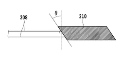
- the groove shape of the termination structures 210-1 to 210-N in this embodiment is such that the angle ( ⁇ ) of the incident surface to the groove is 8 degrees with respect to the propagation direction of the waveguide to be terminated, as shown in FIG. It has become.
- the refractive index of the light shielding material which is a mixture of silicone resin and carbon black, is almost the same as that of quartz glass, but taking into account a slight refractive index difference, the angle ( ⁇ ) is given to reflect the VOA. It is devised so as not to affect the attenuation.
- the optimum angle ( ⁇ ) is determined in consideration of the refractive index of the light shielding material, the arrangement space of the termination structure, the processing accuracy of the groove, and the like.
- Example 2 of the present invention the configuration is the same as in FIGS. 1 and 2A, and the end portions of the dummy ports 208-1 to 208-N of the VOAs 104-1 to N are used as a light shielding material. What mixed the metal fine particle powder used was used. The light incident on the light shielding material is attenuated in light power mainly due to light scattering by the metal fine particles.
- the produced sample is made of a quartz-based optical waveguide produced on a silicon substrate in the same manner as in Example 1, and is terminated with a groove and a light-shielding material introduced to prevent crosstalk due to coupling to an adjacent optical waveguide. 210-1 to N. Also in this example, the crosstalk to the adjacent channel was ⁇ 60 dB or less.
- the angle of the incident surface to the groove of the waveguide to be terminated ( ⁇ in FIG. 3) was set to 15 degrees in consideration of the refractive indexes of the optical waveguide and the light shielding material.
- the return loss on the input side of the VOAs 104-1 to N was 50 dB or more, which was a favorable characteristic.
- Example 3 of the present invention the same configuration as in Example 2 was adopted, and the angle of the incident surface ( ⁇ in FIG. 3) to the groove of the waveguide to be terminated was defined as the Brewster angle.
- Other configurations and light shielding materials are the same as those in the second embodiment.
- the Brewster angle in this example was calculated to be about 50 degrees.
- the influence of crosstalk due to radiated light is further reduced in the entire area of the waveguide substrate.
- the crosstalk to the adjacent channel is ⁇ 65 dB or less, and the return loss on the input side of the VOAs 104-1 to N is also 55 dB or more.
- the present embodiment can be applied to configurations other than the second embodiment such as the first embodiment. Therefore, depending on the space in which the termination structure is arranged in the circuit, it is possible to terminate the excess optical power more effectively by setting the incident angle to the Brewster angle as necessary.
- the configuration is the same as that of the first embodiment.
- the shape of the groove that terminates the dummy port 208 in the horizontal plane of the substrate is smoothly connected without having a vertex.
- a light shielding material was introduced.
- the groove wall surface was formed smoothly, making it difficult for the light shielding material to peel off and improving long-term reliability.
- the effect of reducing crosstalk was the same as in Example 1, and the crosstalk to adjacent channels was ⁇ 60 dB or less. Also in this embodiment, since the incident surface angle to the groove at the terminal portion is 8 degrees, the return loss on the VOA 104-1 to N input side is 50 dB or more.
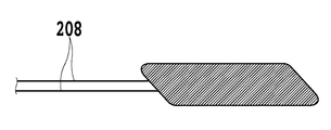
- the configuration is the same as that of the first embodiment, and as shown in FIGS. 5A and 5B, the shape of the optical waveguide at the end portion of the dummy port 208 is a tapered shape. This is because the mode field diameter of the propagating light is enlarged as compared with the case of the optical waveguide having a normal width at other positions, so that the power density of the light incident on the light shielding material is reduced. It is intended. For example, when the light shielding material attenuates the surplus light power of the VOAs 104-1 to N by absorption of light, the light power is converted into heat, thereby increasing the temperature of the light shielding material.
- the rated input optical power may be 200 mW (+23 dBm) or more, and the maximum surplus optical power guided to the VOA dummy port 208 in one channel (during shutdown) Is expected to be about 10 mW (+10 dBm).
- the rising temperature of the light shielding material at that time may exceed 300 degrees depending on the incident mode field diameter, which exceeds the allowable temperature range of the silicone resin.
- the taper length is 100 ⁇ m and the taper width (terminal structure incident side) is 30 ⁇ m.
- the light shielding material by mixing black was used and the resistance to the input power was observed, it was confirmed that the light shielding material was not damaged with respect to the input power of 10 mW (+10 dBm) in any shape.
- the light shielding material was cut in a cross section perpendicular to the light incident direction in the vicinity of the light incident portion and visually confirmed.
- the taper length and width in this embodiment are merely examples, and the respective numerical values are determined by the positional relationship with adjacent waveguides and other circuits and space, and the numerical values described in this embodiment. It is not limited to. That is, the taper length can be arbitrarily determined from about several tens of ⁇ m to about several mm. Further, the mode field diameter can be increased by narrowing the taper width from the normal optical waveguide width. Accordingly, the taper width is set to 0 ⁇ m to 30 ⁇ m, and can be arbitrarily determined from the viewpoint of expanding the mode field diameter as much as possible.
- the interferometer length is 100 ⁇ m and the interferometer width is 30 ⁇ m. It was confirmed that the light shielding material was not damaged even at an input power of 10 mW (+10 dBm).
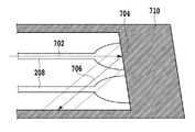
- Example 6 of the present invention as shown in FIG. 7A, the terminated optical waveguide is disposed so as to be surrounded by the groove and the light shielding material in the horizontal plane of the substrate. Thereby, the reflected light generated at the end portion of the optical waveguide is prevented from affecting other circuits.
- the incident light 702 is terminated at the end point 704 of the optical waveguide and a part thereof becomes reflected light 706 and has a certain width (indicated by a dotted line) in the substrate. Is disposed so as to block the reflected light 706.
- Example 2 since a mixture of silicone resin and metal particle powder was used as a light shielding material, a constant reflected light was generated due to a difference in refractive index from quartz glass.
- the angle of the incident surface with respect to the groove of the terminated optical waveguide is set to 15 degrees, most of the reflected light is radiated into the optical waveguide substrate without being coupled to the terminated optical waveguide.
- FIG. 3 or FIG. 4 FIG. 5A, FIG. 5B, FIG. Since it reached the end face of the substrate and radiated into the air without being coupled to the input / output optical fiber, there was no problem in terms of circuit characteristics.
- a light receiving component such as a monitor PD is integrated on a substrate end face or substrate surface in a waveguide type device having an optical waveguide termination structure at an arbitrary position
- the reflected light is received and crosstalk is caused. It may be detected, which causes a problem in circuit characteristics.
- a waveguide type device having a termination structure as shown in FIG. 7A is manufactured, a mixture of silicone resin and metal particle powder is used as a light shielding material, and PD crosstalk is performed at any position (end face, upper and lower surfaces) of the substrate.
- PD crosstalk is performed at any position (end face, upper and lower surfaces) of the substrate.
- the crosstalk may be improved by 10 dB or more depending on the circuit configuration and its position.
- the purpose is to block the reflected light, and therefore the size, position, and shape are arbitrarily determined within a range that does not affect the arrangement of other circuits.
- the portion that terminates the optical waveguide and the portion that shields the reflected light do not necessarily have a continuous shape.
- the structure 714 that blocks the reflected light in the shape shown in FIG. 7B is the termination structure 712 of the optical waveguide. Even if it is discontinuous in figure, the effect by this invention is the same.
- the shape of each of the structures 712 and 714 is formed by a closed curve that has only a smooth curve and a straight line without having a vertex, or the material absorbs or scatters the material. It can be done.
- the waveguide has a tapered shape, but may have a shape other than these.
- FIGS. 8A and 8B are diagrams showing the configuration according to the seventh embodiment of the present invention.
- the configuration for improving the high power resistance of the optical power incident on the termination structure of the waveguide has been described.
- it is necessary to terminate the optical power where the input power reaches several tens of mW. Its resistance was insufficient.
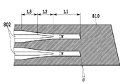
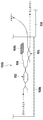
- the optical waveguide 802 to be terminated has a linear taper structure in which the waveguide width becomes narrower toward the end, and the groove shape 810 introduced with the light shielding material as shown in the embodiment 6 is guided.
- the configuration surrounds the periphery of the waveguide.
- the end point of the optical waveguide 802 and the terminal structure 802 are connected with a distance L1 through a gap formed by the cladding layer.
- the distance L1 is set so that the light emitted from the end of the waveguide is sufficiently absorbed by the termination structure, for example, a value of 1 mm or less.
- the length L2 of the taper is set to 500 ⁇ m, and the change rate of the waveguide width is increased, so that the spot size of the light propagating through the waveguide is rapidly changed.
- the distance L1 between the waveguide end point and the termination structure was 750 ⁇ m, and the incident angle ⁇ of light with respect to the termination structure was 15 degrees.
- the groove surrounding the periphery of the optical waveguide to be terminated has a shape gradually approaching the optical waveguide in the L3 portion of FIG. 8A, and in the linear taper portion, from the center of the optical waveguide width depending on the manufacturing error and the required attenuation.
- the distance to the groove is arranged close to the waveguide width from a half of the waveguide width (the groove is in contact with the side wall of the waveguide core).
- the distance L3 is 250 ⁇ m
- the distance from the optical waveguide center to the groove at the linear taper start position is 7 ⁇ m, which is the same as the waveguide width.
- a sample having the configuration shown in FIG. 8A was prepared, and when the resistance against input power was observed using a light shielding material made of a mixture of silicone resin and carbon black, the light shielding material was damaged with respect to the input power of 50 mW (+17 dBm). Confirmed that there is no.
- the spot size conversion at the linear taper is rapidly performed, the emitted light is generated, so that a part of the optical power is attenuated by the light shielding material surrounding the periphery of the optical waveguide. It is possible.
- most of the optical power whose mode field is expanded by the taper propagates on the optical waveguide, but is incident on the termination structure through the gap by the cladding layer at the termination position, so that the optical power is further dispersed and the inside of the light shielding material It is possible to alleviate a rapid temperature rise due to local light absorption at.
- Measured return loss on the VOA input side in the configuration of this example was 55 dB or more. Further, when crosstalk measurement using PD was performed at any position on the substrate, it was ⁇ 60 dB or less at any position with respect to the light intensity input to the terminated optical waveguide.
- the taper of the optical waveguide has a shape in which the waveguide width becomes narrower toward the end, but the width at the end point can be arbitrarily set within a range narrower than the normal waveguide width (other than the taper portion). is there.
- the taper of the optical waveguide has a shape in which the waveguide width becomes narrower toward the end, but the width at the end point can be arbitrarily set within a range narrower than the normal waveguide width (other than the taper portion). is there.
- two types of change rates of different widths in a linear taper shape that narrows the width there are cases where a shape in which two stages of linear tapers are connected is used, but an optical waveguide taper having such a shape is used. This is also included in the scope of the present invention.
- the gap due to the cladding layer between the end point of the optical waveguide and the termination structure is adjusted by the space arranged in the circuit and the incident optical power, and the range is suitably 1 mm or less. That is, it is set so that light emitted from the end of the waveguide is sufficiently absorbed by the termination structure.
- the distance L1 in FIG. 8A may be 0 mm.
- the optical power may be locally incident on the termination structure, so that there is a possibility that sufficient high power resistance cannot be obtained. There is. However, for the purpose of terminating the optical waveguide and suppressing the crosstalk, this can be achieved as long as the light shielding material is not damaged.
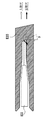
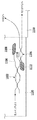
- the groove 812 surrounding the optical waveguide 804 to be terminated is in contact with the optical waveguide core side wall by an arbitrary distance L ′ 4, and this distance L ′ 4 continues to the linear taper start point of the optical waveguide 804.
- the linear taper of the optical waveguide 804 has a shape that narrows toward the end point.
- the end point and the termination structure 812 of the optical waveguide 804 are arranged with a gap formed by the cladding layer.
- the taper length L′ 2 is 500 ⁇ m
- the gap distance L′ 1 is also 500 ⁇ m
- the width W ′ between the grooves in contact with the optical waveguide core side wall is constant until the termination structure 812 is reached. It was.
- a part of the optical power propagating from the time when the groove is in contact with the optical waveguide 804 is radiated and attenuated in the groove, and after further expanding the field toward the termination structure, Attenuates and terminates optical power.
- the optical power can be attenuated more slowly than in the case of the configuration described in the previous embodiments.
- a sample having the configuration shown in FIG. 8B was prepared, and the resistance to the input power was observed using a light shielding material mixed with silicone resin carbon black.
- the light shielding material was not damaged with respect to the input power of 100 mW (+20 dBm). It was confirmed. Further, when the return loss on the input side was measured, it was 55 dB or more. In crosstalk measurement using a PD at any position on the substrate, it was ⁇ 60 dB or less at any location relative to the light intensity input to the terminated optical waveguide.
- the width W ′ of the portion sandwiched between the grooves is constant, but it is possible to further improve the input power resistance by forming the linear taper portion in contact with the optical waveguide core side wall. It is.
- a distance of about 1 to 5 ⁇ m may be provided between the groove and the core side wall via a cladding layer. This is possible as long as the propagation loss of the optical waveguide increases in the vicinity of the groove.
- the waveguide type device it is desirable to absorb the light around the core propagating to the terminal portion by arranging the light shielding groove close to or in contact with the core. If such an arrangement is adopted, the light shielding groove is arranged along the taper, and therefore, as shown in FIG. 9, a manufacturing error of the groove 820 filled with the light shielding material may be a problem.
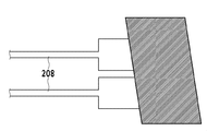
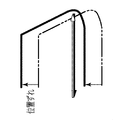
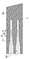
- the end face of the termination structure is cut obliquely (angle ⁇ ) so that light emitted from the waveguide 822 does not return to the waveguide even if it is reflected by the end face.
- the groove corner is actually rounded as shown in FIG. 9B.
- the clad portion 834 in the vicinity of the end face of the termination structure 830 is expanded so that the light from the waveguide 832 does not enter the rounded end face even when the mask is misaligned. Can be.
- the amount of reflection returning to the waveguide 832 can be reduced, and deterioration of the return loss can be suppressed.
- the mask alignment tolerance can be improved, and the productivity is improved.
- the mask alignment accuracy a severe ⁇ m
- the width b about 5 to 10 ⁇ m
- the light emitted from the waveguide Should be taken into account in the width c (10 to 20 ⁇ m, depending on the distance from the end of the waveguide to the end face of the termination structure).
- the width w to be expanded at the end face of the termination structure is w ⁇ a + b + c / 2.
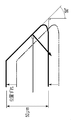
- the taper structure is extended by extending the distances L2 and L′ 2 of the tapered portion in FIG. 8 to L2 ′ and L′ 2 ′ (that is, the taper angle ⁇ is set to a critical angle or less).
- the light shielding material can be prevented from being damaged by the radiation of the tapered portion.
- the termination structure groove 840 is disposed close to the core of the waveguide 842, or the termination structure groove 850 is disposed in contact with the core of the waveguide 852 as shown in FIG. 11B.
- the critical angle of the taper that forms the adiabatic transition structure is about 0.3 degrees when the relative refractive index difference ⁇ is 0.75%.
- the adiabatic transition structure As described above, by adopting the adiabatic transition structure, it is possible to prevent the emitted light from the tapered portion from being generated, but even if the taper angle ⁇ is equal to or greater than the critical angle, the light shielding material by the emitted light from the tapered portion. If the damage is at a level where there is no problem, there is no practical problem.
- FIG. 13A is a diagram showing a configuration of a waveguide type device according to Example 10 of the present invention.
- a waveguide type device substrate 920a in which a waveguide type optical switch (not shown), VOA 902, and WinC 904 are integrated, and a waveguide type device substrate 930 in which an AWG and a monitor PD are integrated are directly connected. And constitutes the main function of the ROADM system.
- the dummy port 906 of the VOA 902 is terminated with a termination structure 908a made of a groove and a light shielding material.
- a termination structure 908a made of a groove and a light shielding material.
- both the optical switch and the AWG are configured by the same optical waveguide as the VOA, and the monitor PD is connected to the end face of the substrate. .
- the optical switch has the functions of the 2 ⁇ 1 switches 1408-1 to 1408-1 in FIG. 18, and is inserted (added) from the DEMUX (wavelength demultiplexed) optical signal path (main path) or the lower layer network. One of the optical signal paths (add paths) is selected. The optical level of the selected optical signal is adjusted by the VOA 902, and the optical signal is connected to the MUX (wavelength multiplexing) AWG via the WinC 904.
- epoxy resin and carbon black were used for the light shielding material of the termination structure 908a for terminating the dummy port 906 of the VOA.
- both were -60 dB or less.
- the incident surface angle of the optical waveguide is 0 degree with respect to the termination structure 908a.
- the return loss measured on the optical switch input side is 45 dB or more.
- the incident surface angle with respect to the termination structure 908b was set to 8 degrees, the return loss was 50 dB or more.
- the angle of the incident surface is set to 0 degree in consideration of the size of the groove in the substrate horizontal plane. Even in such a case, sufficient return loss characteristics can be obtained.
- a higher specification is required, it is necessary to adopt a configuration in which reflected light is not coupled to the terminated optical waveguide, and the Brewster angle or the like is optimal.
- the optical switch and the VOA 902 are described as separate circuits.
- the functions of the optical switch and the VOA may be simultaneously realized using the same MZI, and the configuration shown in FIG. 13A is limited by the present invention. It does not indicate a typical configuration.
- Patent Document 1 or Non-Patent Document 1 can be referred to as a configuration example of the ROADM optical switch and the VOA.
- the through-path side optical switch and the add-path side optical switch are each composed of MZIs that are directly connected in two stages.
- the dummy ports derived from the respective MZIs are terminated individually or collectively by the termination structure composed of the groove and the light shielding material according to the present invention so that the surplus optical power does not affect other circuits. Is possible.
- FIG. 15 is a diagram showing a configuration of a waveguide type device according to Example 11 of the present invention. Similar to Example 10, in this device, a waveguide type device substrate 1120 in which a waveguide type optical switch, VOA 1102 and WINC 1104 are integrated, and a waveguide type device substrate 1130 in which an AWG and a monitor PD are integrated are directly connected. It constitutes the main function of the ROADM system.
- the dummy port 1106 of the VOA 1102 is terminated with a termination structure 1108 made of a groove and a light shielding material
- the input side dummy port 1110 of the WINC 1104 is also terminated by a termination structure 1112 made of a groove and a light shielding material.
- the light shielding material was a mixture of a silicone resin as a base material and metal particle powder.
- the crosstalk component caused by the connection loss that occurs when connected to another waveguide device or optical fiber at the input portion of the waveguide type device substrate 1120, or excess generated on the optical waveguide of the optical switch and VOA 1102 It is possible to suppress the crosstalk component caused by the loss from being coupled to the input side dummy port 1110 of the WINC and affecting the coupling rate as a coupler.
- the effect of suppressing the crosstalk by the termination structure 1108 of the dummy port 1106 of the VOA 1102 was confirmed, and the crosstalk was ⁇ 60 dB or less at any location. Further, the return loss on the input side of the optical switch was also 50 dB or more.
- the termination of the input-side dummy port in this embodiment is not limited to WINC.
- the optical-side switch having MZI as a basic element, or an optical circuit having a dummy port on the input side, such as a VOA By terminating, it is possible to obtain effects such as suppression of the influence of crosstalk.
- FIG. 16 shows an example of an optical splitter.
- the configuration of FIG. In this case, the 1 ⁇ 8 splitter 1200 is a basic configuration, and the termination structure 1204 according to the present invention is applied to the two optical waveguides 1202 that are not used as output ports, thereby suppressing crosstalk in other output ports.
- a 1 ⁇ 6 splitter based on the configuration of FIG. 16 was manufactured using an optical waveguide made of silica glass manufactured on a silicon substrate.
- the deviation between the ports of the output power in the entire wavelength range was about 0.5 dB, which was a favorable characteristic. It was.
- FIG. 17A is an example of AWG.
- the output side optical waveguide is terminated by the termination structure 1304 of the present invention at regular intervals of the output port, thereby separating the optical signal for each group of wavelengths.
- N is a natural number
- the termination structure 1304 of the present invention at regular intervals of the output port, thereby separating the optical signal for each group of wavelengths.
- signal processing such that the wavelength groups are separated from each other by sandwiching one ITU grid G1 to G4 (see FIG. 17B).
- an AWG substrate based on the configuration of FIG. 17A was fabricated using a polymer waveguide fabricated on a silicon substrate.
- the AWG 1302 of this embodiment is configured to separate the wavelength group for eight wavelengths into five groups, and 44 optical waveguides are arranged on the output side with respect to one input waveguide, of which eight Each wavelength group is separated by terminating one optical waveguide.
- the total number of wavelengths (terminated wavelengths) sandwiched between the two wavelength groups is four, but in any case, the crosstalk at all ports other than the terminated ports is -40 dB or less.
- the waveguide type device made of the silica glass and the polymer material on the silicon substrate has been described.
- other materials constituting the waveguide type device for example, ion diffusion type niobium are described.
- the present invention can be applied to all waveguide type thermo-optic circuits using a lithium acid waveguide or the like.
- the depth of the groove is not particularly mentioned.
- the depth reaching the silicon substrate is used. Is desirable.
- the effect of the present invention is clear, and the depth is expressed by the core on the groove wall surface of the end portion of the optical waveguide. As a matter of course, it is of course necessary to be at a minimum, but the configuration of the present invention is not limited to a specific depth.
Landscapes
- Physics & Mathematics (AREA)
- General Physics & Mathematics (AREA)
- Optics & Photonics (AREA)
- Engineering & Computer Science (AREA)
- Microelectronics & Electronic Packaging (AREA)
- Power Engineering (AREA)
- Plasma & Fusion (AREA)
- Optical Integrated Circuits (AREA)
- Optical Modulation, Optical Deflection, Nonlinear Optics, Optical Demodulation, Optical Logic Elements (AREA)
Abstract
Description
102 光ファイバアレイ
104-1~N VOA
106-1~N 光カプラ
108 PD
110 AWG
112 光ファイバ
120 基板
130 基板
202-1~N MZI
204-1~N MZI
206a メインポート
206b タップポート
208-1~N ダミーポート
210-1~N 終端構造
702 入射光
704 終点
706 反射光
710 終端構造
712 終端構造
714 構造
802 光導波路
804 光導波路
810 終端構造
812 終端構造
820 終端構造
822 光導波路
830 終端構造
832 光導波路
834 拡げたクラッド部分
840 終端構造
842 光導波路
850 終端構造
852 光導波路
900a,900b 導波路型デバイス
902 VOA
904 WINC
906 ダミーポート
908a,908b 終端構造
920a,920b 基板
930 基板
1102 VOA
1104 WINC
1106 ダミーポート
1108 終端構造
1110 ダミーポート
1112 終端構造
1120 基板
1130 基板
1200 1×8スプリッタ
1202 光導波路
1204 終端構造
1302 AWG
1304 終端構造
1400 モジュール
1402 光カプラ
1404 波長合分波フィルタ
1406 波長合分波フィルタ
1408-1~N 光スイッチ
1410-1~N VOA
1412-1~N 光カプラ
1414-1~N PD
1416 波長合分波フィルタ
1420 基板
1430 基板
1500 VOA
1502a,1502b ポート
1504 方向性結合器
1506a,1506b アーム導波路
1508 方向性結合器
1510a,1510b ポート
1512a,1512b 薄膜ヒータ
1514 断熱溝
1516 電極パッド
1518 電極パッド
1520 シリコン基板
1522 クラッド
1524 コア
1602 VOA
1604 光カプラ
1606 基板
1608 基板
1610 光導波路
Claims (7)
- 導波路型デバイスであって、
導波路端部からの光を終端するために遮光材が充填された終端構造を備え、
前記終端構造は、前記導波路端部からの光に対する入射角が傾くように構成され、
前記導波路端部は、終端に向かって導波路幅が狭くなるテーパ部を有し、
前記終端構造は、前記導波路端部を囲い、前記テーパ部に近接または接して配置され、前記終端構造によって挟まれた部分の幅を前記導波路端部の終端に対向する面において拡げることを特徴とする導波路型デバイス。 - 請求項1に記載の導波路型デバイスであって、
前記テーパ部のテーパ角は、略、断熱遷移となる臨界角以下であることを特徴とする導波路型デバイス。 - 導波路型デバイスであって、
導波路端部からの光を終端するために遮光材が充填された終端構造を備え、
前記終端構造は、前記導波路端部からの光に対する入射角が傾くように構成され、
前記導波路端部は、終端に向かって導波路幅が狭くなるテーパ部を有し、
前記終端構造は、前記導波路端部を囲い、前記テーパ部に近接または接して配置され、
前記テーパ部のテーパ角は、略、断熱遷移となる臨界角以下であることを特徴とする導波路型デバイス。 - 請求項1から3のいずれかに記載の導波路型デバイスであって、前記入射角は、略、ブリュースタ角以上であることを特徴とする導波路型デバイス。
- 請求項1から4のいずれかに記載の導波路型デバイスであって、前記遮光材は、前記導波路端部からの光を吸収または散乱する材料からなることを特徴とする導波路型デバイス。
- 請求項1から5のいずれかに記載の導波路型デバイスであって、マッハツェンダ型の光スイッチ、可変減衰器、光スプリッタ、およびアレイ導波路回折格子の少なくともいずれか1つを含むことを特徴とする導波路型デバイス。
- 請求項1から6のいずれかに記載の導波路型デバイスを用いてマルチチップ集積化したモジュール。
Priority Applications (4)
| Application Number | Priority Date | Filing Date | Title |
|---|---|---|---|
| US13/511,118 US9020307B2 (en) | 2009-11-26 | 2010-11-26 | Optical waveguide device and module |
| CN201080053387.7A CN102667556B (zh) | 2009-11-26 | 2010-11-26 | 光波导器件以及模块 |
| US14/669,348 US9684129B2 (en) | 2009-11-26 | 2015-03-26 | Optical waveguide device and module |
| US15/416,853 US10126502B2 (en) | 2009-11-26 | 2017-01-26 | Optical waveguide device and module |
Applications Claiming Priority (2)
| Application Number | Priority Date | Filing Date | Title |
|---|---|---|---|
| JP2009-268814 | 2009-11-26 | ||
| JP2009268814A JP5074477B2 (ja) | 2009-11-26 | 2009-11-26 | 光導波路デバイス |
Related Child Applications (2)
| Application Number | Title | Priority Date | Filing Date |
|---|---|---|---|
| US13/511,118 A-371-Of-International US9020307B2 (en) | 2009-11-26 | 2010-11-26 | Optical waveguide device and module |
| US14/669,348 Continuation US9684129B2 (en) | 2009-11-26 | 2015-03-26 | Optical waveguide device and module |
Publications (1)
| Publication Number | Publication Date |
|---|---|
| WO2011065014A1 true WO2011065014A1 (ja) | 2011-06-03 |
Family
ID=44066119
Family Applications (1)
| Application Number | Title | Priority Date | Filing Date |
|---|---|---|---|
| PCT/JP2010/006913 Ceased WO2011065014A1 (ja) | 2009-11-26 | 2010-11-26 | 光導波路デバイスおよびモジュール |
Country Status (4)
| Country | Link |
|---|---|
| US (3) | US9020307B2 (ja) |
| JP (1) | JP5074477B2 (ja) |
| CN (2) | CN104345392B (ja) |
| WO (1) | WO2011065014A1 (ja) |
Cited By (2)
| Publication number | Priority date | Publication date | Assignee | Title |
|---|---|---|---|---|
| CN103858035A (zh) * | 2011-10-28 | 2014-06-11 | Hoya美国公司 | 波导衬底上用于衰减光源的光波导分路器 |
| JP6430071B1 (ja) * | 2017-05-26 | 2018-11-28 | 三菱電機株式会社 | 多モード干渉型合分波器、および、これを用いた光学素子 |
Families Citing this family (37)
| Publication number | Priority date | Publication date | Assignee | Title |
|---|---|---|---|---|
| JP5497996B2 (ja) * | 2008-05-26 | 2014-05-21 | 日本電信電話株式会社 | 導波路型デバイスにおける導波路終端方法 |
| JP5270998B2 (ja) * | 2008-07-30 | 2013-08-21 | Nttエレクトロニクス株式会社 | 平面光導波回路 |
| JP6207398B2 (ja) * | 2011-01-28 | 2017-10-04 | コーニンクレッカ フィリップス エヌ ヴェKoninklijke Philips N.V. | 形状検知光ファイバの先端反射低減 |
| US20150212271A1 (en) * | 2012-12-11 | 2015-07-30 | Acacia Communications Inc. | Optical waveguide terminators with doped waveguides |
| US10191213B2 (en) | 2014-01-09 | 2019-01-29 | Globalfoundries Inc. | Shielding structures between optical waveguides |
| US10248002B2 (en) * | 2015-03-30 | 2019-04-02 | Nec Corporation | Optical circuit, and optical switch using same |
| WO2017031072A1 (en) * | 2015-08-14 | 2017-02-23 | Skorpios Technologies, Inc. | Broadband high-speed wavelength-division multiplexed receiver using multiple photodetectors per channel |
| US9496921B1 (en) * | 2015-09-09 | 2016-11-15 | Cpg Technologies | Hybrid guided surface wave communication |
| FI4002724T3 (fi) | 2015-12-13 | 2025-09-30 | Gxc Llc | Häiriönpoistomenetelmiä ja -laite |
| US9941957B2 (en) * | 2016-01-07 | 2018-04-10 | Luxtera, Inc. | Method and system for connectionless integrated optical receiver and transmitter test |
| JP6623102B2 (ja) * | 2016-03-31 | 2019-12-18 | 古河電気工業株式会社 | 光導波回路装置 |
| US10257746B2 (en) | 2016-07-16 | 2019-04-09 | GenXComm, Inc. | Interference cancellation methods and apparatus |
| CN109642986B (zh) * | 2016-09-06 | 2020-12-01 | Agc株式会社 | 树脂光波导以及复合光波导 |
| SG10201900248VA (en) * | 2018-01-12 | 2019-08-27 | Rain Tree Photonics Pte Ltd | Scavenging photodetection device |
| EP3561561B1 (en) * | 2018-04-26 | 2022-04-13 | Huawei Technologies Co., Ltd. | Optical splitter including a trident structure |
| US12149052B2 (en) * | 2018-06-03 | 2024-11-19 | DustPhotonics | Method and device for aligning a laser and a waveguide |
| CN111352187B (zh) * | 2018-12-21 | 2022-05-20 | 中兴光电子技术有限公司 | 一种波导终结器、光通信器件及光终结的方法 |
| US11150409B2 (en) | 2018-12-27 | 2021-10-19 | GenXComm, Inc. | Saw assisted facet etch dicing |
| US10527793B1 (en) * | 2019-01-24 | 2020-01-07 | Elenion Technologies, Llc | Dump terminator |
| WO2020181938A1 (zh) * | 2019-03-14 | 2020-09-17 | 青岛海信宽带多媒体技术有限公司 | 一种光模块 |
| WO2021005723A1 (ja) * | 2019-07-09 | 2021-01-14 | 日本電信電話株式会社 | 光合波回路 |
| US10727945B1 (en) | 2019-07-15 | 2020-07-28 | GenXComm, Inc. | Efficiently combining multiple taps of an optical filter |
| KR20210018726A (ko) * | 2019-08-09 | 2021-02-18 | 한국전자통신연구원 | 코히어런트 광수신기 및 그의 제조 방법 |
| US11215755B2 (en) | 2019-09-19 | 2022-01-04 | GenXComm, Inc. | Low loss, polarization-independent, large bandwidth mode converter for edge coupling |
| US11539394B2 (en) | 2019-10-29 | 2022-12-27 | GenXComm, Inc. | Self-interference mitigation in in-band full-duplex communication systems |
| US11371843B2 (en) | 2020-07-02 | 2022-06-28 | Anello Photonics, Inc. | Integration of photonics optical gyroscopes with micro-electro-mechanical sensors |
| US11796737B2 (en) | 2020-08-10 | 2023-10-24 | GenXComm, Inc. | Co-manufacturing of silicon-on-insulator waveguides and silicon nitride waveguides for hybrid photonic integrated circuits |
| US12001065B1 (en) | 2020-11-12 | 2024-06-04 | ORCA Computing Limited | Photonics package with tunable liquid crystal lens |
| CN114578481B (zh) * | 2020-11-28 | 2023-07-07 | 华为技术有限公司 | 一种模斑转换装置及相关方法 |
| WO2022178182A1 (en) | 2021-02-18 | 2022-08-25 | GenXComm, Inc. | Maximizing efficiency of communication systems with self-interference cancellation subsystems |
| US11719898B2 (en) * | 2021-03-03 | 2023-08-08 | Marvell Asia Pte Ltd. | Methods for co-packaging optical modules on switch package substrate |
| EP4331120A1 (en) | 2021-04-29 | 2024-03-06 | Genxcomm, Inc. | Self-interference cancellation subsystems for mesh network nodes |
| CN113740979A (zh) * | 2021-08-17 | 2021-12-03 | 武汉光迅科技股份有限公司 | 光器件及光模块 |
| US11838056B2 (en) | 2021-10-25 | 2023-12-05 | GenXComm, Inc. | Hybrid photonic integrated circuits for ultra-low phase noise signal generators |
| US20230125660A1 (en) * | 2022-10-17 | 2023-04-27 | Wenhua Lin | Technologies for optical demultiplexing with backwards compatibility |
| CN118795606A (zh) * | 2023-04-14 | 2024-10-18 | 华为技术有限公司 | 多芯光纤光衰减器和光放大装置 |
| US12487401B2 (en) * | 2023-05-20 | 2025-12-02 | Globalfoundries U.S. Inc. | Photonic integrated circuit including optical absorber for terminal end of waveguide |
Citations (4)
| Publication number | Priority date | Publication date | Assignee | Title |
|---|---|---|---|---|
| JP2001330746A (ja) * | 2000-03-13 | 2001-11-30 | Matsushita Electric Ind Co Ltd | 光モジュールおよびその製造方法、ならびに光回路装置 |
| JP2003270460A (ja) * | 2002-03-15 | 2003-09-25 | Nippon Telegr & Teleph Corp <Ntt> | アレイ導波路格子型波長合分波器を含む集積光回路 |
| JP2006235380A (ja) * | 2005-02-25 | 2006-09-07 | Nippon Telegr & Teleph Corp <Ntt> | モードスプリッタおよび光回路 |
| WO2009145199A1 (ja) * | 2008-05-26 | 2009-12-03 | 日本電信電話株式会社 | 導波路型デバイスおよびモジュール |
Family Cites Families (10)
| Publication number | Priority date | Publication date | Assignee | Title |
|---|---|---|---|---|
| JPH04211209A (ja) * | 1990-03-07 | 1992-08-03 | Toshiba Corp | 集積化光半導体素子 |
| JPH04361030A (ja) | 1991-06-07 | 1992-12-14 | Toyoda Gosei Co Ltd | ガラスランの製造方法 |
| US6480639B2 (en) * | 1997-09-26 | 2002-11-12 | Nippon Telegraph And Telephone Corp. | Optical module |
| US20010053260A1 (en) | 2000-03-13 | 2001-12-20 | Toshiyuki Takizawa | Optical module and method for producing the same, and optical circuit device |
| JP3755762B2 (ja) | 2002-07-05 | 2006-03-15 | 日本電信電話株式会社 | 光分岐挿入スイッチ及び光分岐挿入スイッチの出力光強度調整方法 |
| US7113676B2 (en) * | 2003-12-04 | 2006-09-26 | David Piede | Planar waveguide optical isolator in thin silicon-on-isolator (SOI) structure |
| CN200968996Y (zh) * | 2006-08-09 | 2007-10-31 | 陈谷红 | 多信道可调光衰减器 |
| JP2008293020A (ja) * | 2007-05-25 | 2008-12-04 | Jds Uniphase Corp | 断熱導波路遷移 |
| US7974504B2 (en) * | 2008-03-28 | 2011-07-05 | Infinera Corporation | Reflection suppression in a photonic integrated circuit |
| JP5399693B2 (ja) * | 2008-07-14 | 2014-01-29 | 日本電信電話株式会社 | 光波長合分波回路 |
-
2009
- 2009-11-26 JP JP2009268814A patent/JP5074477B2/ja active Active
-
2010
- 2010-11-26 US US13/511,118 patent/US9020307B2/en active Active
- 2010-11-26 WO PCT/JP2010/006913 patent/WO2011065014A1/ja not_active Ceased
- 2010-11-26 CN CN201410697531.0A patent/CN104345392B/zh active Active
- 2010-11-26 CN CN201080053387.7A patent/CN102667556B/zh active Active
-
2015
- 2015-03-26 US US14/669,348 patent/US9684129B2/en active Active
-
2017
- 2017-01-26 US US15/416,853 patent/US10126502B2/en active Active
Patent Citations (4)
| Publication number | Priority date | Publication date | Assignee | Title |
|---|---|---|---|---|
| JP2001330746A (ja) * | 2000-03-13 | 2001-11-30 | Matsushita Electric Ind Co Ltd | 光モジュールおよびその製造方法、ならびに光回路装置 |
| JP2003270460A (ja) * | 2002-03-15 | 2003-09-25 | Nippon Telegr & Teleph Corp <Ntt> | アレイ導波路格子型波長合分波器を含む集積光回路 |
| JP2006235380A (ja) * | 2005-02-25 | 2006-09-07 | Nippon Telegr & Teleph Corp <Ntt> | モードスプリッタおよび光回路 |
| WO2009145199A1 (ja) * | 2008-05-26 | 2009-12-03 | 日本電信電話株式会社 | 導波路型デバイスおよびモジュール |
Cited By (4)
| Publication number | Priority date | Publication date | Assignee | Title |
|---|---|---|---|---|
| CN103858035A (zh) * | 2011-10-28 | 2014-06-11 | Hoya美国公司 | 波导衬底上用于衰减光源的光波导分路器 |
| JP6430071B1 (ja) * | 2017-05-26 | 2018-11-28 | 三菱電機株式会社 | 多モード干渉型合分波器、および、これを用いた光学素子 |
| WO2018216249A1 (ja) * | 2017-05-26 | 2018-11-29 | 三菱電機株式会社 | 多モード干渉型合分波器、および、これを用いた光学素子 |
| US10983272B2 (en) | 2017-05-26 | 2021-04-20 | Mitsubishi Electric Corporation | Multi-mode interference multiplexer/demultiplexer and optical element using the same |
Also Published As
| Publication number | Publication date |
|---|---|
| US20170146742A1 (en) | 2017-05-25 |
| US20150205043A1 (en) | 2015-07-23 |
| JP2011112844A (ja) | 2011-06-09 |
| US10126502B2 (en) | 2018-11-13 |
| CN104345392B (zh) | 2017-06-30 |
| CN104345392A (zh) | 2015-02-11 |
| US9684129B2 (en) | 2017-06-20 |
| CN102667556B (zh) | 2014-12-17 |
| CN102667556A (zh) | 2012-09-12 |
| US20120251041A1 (en) | 2012-10-04 |
| JP5074477B2 (ja) | 2012-11-14 |
| US9020307B2 (en) | 2015-04-28 |
Similar Documents
| Publication | Publication Date | Title |
|---|---|---|
| JP5074477B2 (ja) | 光導波路デバイス | |
| JP5497996B2 (ja) | 導波路型デバイスにおける導波路終端方法 | |
| US10656333B2 (en) | Two-stage adiabatically coupled photonic systems | |
| KR100897887B1 (ko) | 광섬유어레이를 이용한 평판형 광도파로 소자와 능동소자의하이브리드 집적구조 | |
| Nishi et al. | Monolithic integration of a silica-based arrayed waveguide grating filter and silicon variable optical attenuators based on p–i–n carrier-injection structure | |
| JP2006058858A (ja) | 導波路型熱光学位相シフタおよびその光回路 | |
| Nasu et al. | Ultrasmall 100 GHz 40-channel VMUX/DEMUX based on single-chip 2.5%-Δ PLC | |
| JP3710426B2 (ja) | 光強度モニタ回路 | |
| JP2007163825A (ja) | 導波路型熱光学回路 | |
| CN216013727U (zh) | 一种平面光波导芯片 | |
| JP4699435B2 (ja) | 光モジュール | |
| Ogawa et al. | Single-chip 16-ch variable attenuator multiplexer (V-AWG) with stacked PD-array using integrated micro-mirrors on PLC | |
| Abe et al. | Compact single-chip AWG multiplexer with variable attenuator integrated micro-mirror and stacked PD-array |
Legal Events
| Date | Code | Title | Description |
|---|---|---|---|
| WWE | Wipo information: entry into national phase |
Ref document number: 201080053387.7 Country of ref document: CN |
|
| 121 | Ep: the epo has been informed by wipo that ep was designated in this application |
Ref document number: 10832863 Country of ref document: EP Kind code of ref document: A1 |
|
| WWE | Wipo information: entry into national phase |
Ref document number: 13511118 Country of ref document: US |
|
| NENP | Non-entry into the national phase |
Ref country code: DE |
|
| 122 | Ep: pct application non-entry in european phase |
Ref document number: 10832863 Country of ref document: EP Kind code of ref document: A1 |