WO2011058892A1 - スイッチング電源回路 - Google Patents
スイッチング電源回路 Download PDFInfo
- Publication number
- WO2011058892A1 WO2011058892A1 PCT/JP2010/069305 JP2010069305W WO2011058892A1 WO 2011058892 A1 WO2011058892 A1 WO 2011058892A1 JP 2010069305 W JP2010069305 W JP 2010069305W WO 2011058892 A1 WO2011058892 A1 WO 2011058892A1
- Authority
- WO
- WIPO (PCT)
- Prior art keywords
- main
- slave
- reactor
- power supply
- diode
- Prior art date
Links
Images

Classifications
-
- H—ELECTRICITY
- H02—GENERATION; CONVERSION OR DISTRIBUTION OF ELECTRIC POWER
- H02M—APPARATUS FOR CONVERSION BETWEEN AC AND AC, BETWEEN AC AND DC, OR BETWEEN DC AND DC, AND FOR USE WITH MAINS OR SIMILAR POWER SUPPLY SYSTEMS; CONVERSION OF DC OR AC INPUT POWER INTO SURGE OUTPUT POWER; CONTROL OR REGULATION THEREOF
- H02M3/00—Conversion of dc power input into dc power output
- H02M3/02—Conversion of dc power input into dc power output without intermediate conversion into ac
- H02M3/04—Conversion of dc power input into dc power output without intermediate conversion into ac by static converters
- H02M3/10—Conversion of dc power input into dc power output without intermediate conversion into ac by static converters using discharge tubes with control electrode or semiconductor devices with control electrode
- H02M3/145—Conversion of dc power input into dc power output without intermediate conversion into ac by static converters using discharge tubes with control electrode or semiconductor devices with control electrode using devices of a triode or transistor type requiring continuous application of a control signal
- H02M3/155—Conversion of dc power input into dc power output without intermediate conversion into ac by static converters using discharge tubes with control electrode or semiconductor devices with control electrode using devices of a triode or transistor type requiring continuous application of a control signal using semiconductor devices only
- H02M3/156—Conversion of dc power input into dc power output without intermediate conversion into ac by static converters using discharge tubes with control electrode or semiconductor devices with control electrode using devices of a triode or transistor type requiring continuous application of a control signal using semiconductor devices only with automatic control of output voltage or current, e.g. switching regulators
- H02M3/158—Conversion of dc power input into dc power output without intermediate conversion into ac by static converters using discharge tubes with control electrode or semiconductor devices with control electrode using devices of a triode or transistor type requiring continuous application of a control signal using semiconductor devices only with automatic control of output voltage or current, e.g. switching regulators including plural semiconductor devices as final control devices for a single load
- H02M3/1584—Conversion of dc power input into dc power output without intermediate conversion into ac by static converters using discharge tubes with control electrode or semiconductor devices with control electrode using devices of a triode or transistor type requiring continuous application of a control signal using semiconductor devices only with automatic control of output voltage or current, e.g. switching regulators including plural semiconductor devices as final control devices for a single load with a plurality of power processing stages connected in parallel
-
- H—ELECTRICITY
- H02—GENERATION; CONVERSION OR DISTRIBUTION OF ELECTRIC POWER
- H02M—APPARATUS FOR CONVERSION BETWEEN AC AND AC, BETWEEN AC AND DC, OR BETWEEN DC AND DC, AND FOR USE WITH MAINS OR SIMILAR POWER SUPPLY SYSTEMS; CONVERSION OF DC OR AC INPUT POWER INTO SURGE OUTPUT POWER; CONTROL OR REGULATION THEREOF
- H02M1/00—Details of apparatus for conversion
- H02M1/42—Circuits or arrangements for compensating for or adjusting power factor in converters or inverters
- H02M1/4208—Arrangements for improving power factor of AC input
- H02M1/4225—Arrangements for improving power factor of AC input using a non-isolated boost converter
-
- H—ELECTRICITY
- H02—GENERATION; CONVERSION OR DISTRIBUTION OF ELECTRIC POWER
- H02M—APPARATUS FOR CONVERSION BETWEEN AC AND AC, BETWEEN AC AND DC, OR BETWEEN DC AND DC, AND FOR USE WITH MAINS OR SIMILAR POWER SUPPLY SYSTEMS; CONVERSION OF DC OR AC INPUT POWER INTO SURGE OUTPUT POWER; CONTROL OR REGULATION THEREOF
- H02M3/00—Conversion of dc power input into dc power output
- H02M3/02—Conversion of dc power input into dc power output without intermediate conversion into ac
- H02M3/04—Conversion of dc power input into dc power output without intermediate conversion into ac by static converters
- H02M3/10—Conversion of dc power input into dc power output without intermediate conversion into ac by static converters using discharge tubes with control electrode or semiconductor devices with control electrode
- H02M3/145—Conversion of dc power input into dc power output without intermediate conversion into ac by static converters using discharge tubes with control electrode or semiconductor devices with control electrode using devices of a triode or transistor type requiring continuous application of a control signal
- H02M3/155—Conversion of dc power input into dc power output without intermediate conversion into ac by static converters using discharge tubes with control electrode or semiconductor devices with control electrode using devices of a triode or transistor type requiring continuous application of a control signal using semiconductor devices only
- H02M3/156—Conversion of dc power input into dc power output without intermediate conversion into ac by static converters using discharge tubes with control electrode or semiconductor devices with control electrode using devices of a triode or transistor type requiring continuous application of a control signal using semiconductor devices only with automatic control of output voltage or current, e.g. switching regulators
- H02M3/158—Conversion of dc power input into dc power output without intermediate conversion into ac by static converters using discharge tubes with control electrode or semiconductor devices with control electrode using devices of a triode or transistor type requiring continuous application of a control signal using semiconductor devices only with automatic control of output voltage or current, e.g. switching regulators including plural semiconductor devices as final control devices for a single load
- H02M3/1584—Conversion of dc power input into dc power output without intermediate conversion into ac by static converters using discharge tubes with control electrode or semiconductor devices with control electrode using devices of a triode or transistor type requiring continuous application of a control signal using semiconductor devices only with automatic control of output voltage or current, e.g. switching regulators including plural semiconductor devices as final control devices for a single load with a plurality of power processing stages connected in parallel
- H02M3/1586—Conversion of dc power input into dc power output without intermediate conversion into ac by static converters using discharge tubes with control electrode or semiconductor devices with control electrode using devices of a triode or transistor type requiring continuous application of a control signal using semiconductor devices only with automatic control of output voltage or current, e.g. switching regulators including plural semiconductor devices as final control devices for a single load with a plurality of power processing stages connected in parallel switched with a phase shift, i.e. interleaved
-
- Y—GENERAL TAGGING OF NEW TECHNOLOGICAL DEVELOPMENTS; GENERAL TAGGING OF CROSS-SECTIONAL TECHNOLOGIES SPANNING OVER SEVERAL SECTIONS OF THE IPC; TECHNICAL SUBJECTS COVERED BY FORMER USPC CROSS-REFERENCE ART COLLECTIONS [XRACs] AND DIGESTS
- Y02—TECHNOLOGIES OR APPLICATIONS FOR MITIGATION OR ADAPTATION AGAINST CLIMATE CHANGE
- Y02B—CLIMATE CHANGE MITIGATION TECHNOLOGIES RELATED TO BUILDINGS, e.g. HOUSING, HOUSE APPLIANCES OR RELATED END-USER APPLICATIONS
- Y02B70/00—Technologies for an efficient end-user side electric power management and consumption
- Y02B70/10—Technologies improving the efficiency by using switched-mode power supplies [SMPS], i.e. efficient power electronics conversion e.g. power factor correction or reduction of losses in power supplies or efficient standby modes
-
- Y—GENERAL TAGGING OF NEW TECHNOLOGICAL DEVELOPMENTS; GENERAL TAGGING OF CROSS-SECTIONAL TECHNOLOGIES SPANNING OVER SEVERAL SECTIONS OF THE IPC; TECHNICAL SUBJECTS COVERED BY FORMER USPC CROSS-REFERENCE ART COLLECTIONS [XRACs] AND DIGESTS
- Y02—TECHNOLOGIES OR APPLICATIONS FOR MITIGATION OR ADAPTATION AGAINST CLIMATE CHANGE
- Y02P—CLIMATE CHANGE MITIGATION TECHNOLOGIES IN THE PRODUCTION OR PROCESSING OF GOODS
- Y02P80/00—Climate change mitigation technologies for sector-wide applications
- Y02P80/10—Efficient use of energy, e.g. using compressed air or pressurized fluid as energy carrier
Definitions
- the present invention relates to a switching power supply circuit, and more particularly to a power factor correction circuit.
- Non-Patent Document 1 describes a power factor correction circuit.
- a main power factor correction circuit and a slave factor correction circuit are provided.
- the main power factor improvement circuit and the power factor improvement circuit are connected to the same DC power source, and the main power factor improvement circuit and the power factor improvement circuit are connected in parallel to each other. These have the same configuration.
- the main power factor improvement circuit and the power factor improvement circuit are so-called step-up type chopper circuits, which have a reactor, a diode, and a switching element.
- a MOS field effect transistor is employed as such a switching element.
- the switching element of the power factor correction circuit is turned on when a predetermined period has elapsed from when the switching element of the main power factor improvement circuit is turned on. That is, such a power factor correction circuit operates by so-called interleaving.
- Patent Documents 1 and 2 are disclosed as techniques related to the present invention.
- Non-Patent Document 1 employs a MOS field effect transistor as a switching element, the power factor correction circuit of Non-Patent Document 1 is not suitable for large current applications.
- Non-Patent Document 1 In order to apply the power factor correction circuit of Non-Patent Document 1 to a large current application, it is conceivable to employ an insulated gate bipolar transistor as introduced in Patent Document 2 as a switching element.
- the power factor correction circuit of Non-Patent Document 1 When the power factor correction circuit of Non-Patent Document 1 is employed for a large current application, it causes an increase in conduction loss caused by each component. Therefore, for example, a diode having a low forward drop voltage is employed in the switching power supply circuit. In the diode, since the forward drop voltage and the reverse recovery characteristic are in a trade-off relationship, a reverse recovery current can flow through the diode. There is a possibility that a reverse voltage is applied to the switching element due to the reverse recovery current.
- an object of the present invention is to provide a power factor correction circuit that eliminates or reduces a reverse voltage applied to a switching element employed in a switching power supply circuit.
- a first aspect of the switching power supply circuit according to the present invention includes a low power supply line (LL), a main power supply line and a sub power supply line (LH1, LH2) to which a higher potential is applied than the low power supply line,
- the main reactor and the sub reactors (L1, L2) provided on the main power line and the sub power line, respectively, and having the same inductance, and the main reactor and the sub power line on the main power line and the sub power line, respectively.
- An emitter is provided between the point between the diode and the low power supply line with the emitter directed toward the low power supply line, and the current flows through the main reactor reaches zero.
- T 1 An emitter is provided toward the low power supply line between the main insulated gate bipolar transistor (S1) that is non-conductive after the passage, the point between the slave reactor and the slave diode, and the low power supply line.
- the first insulated gate bipolar transistor is turned on as one of the conditions that a certain period shorter than the period until the next turned on is passed, and the second period shorter than the first period ( t2)
- a second aspect of the switching power supply circuit according to the present invention is the switching power supply circuit according to the first aspect, wherein the switching power supply circuit is connected in parallel to the main insulated gate bipolar transistor (S1), and the anode is connected to the main power supply line (LH1). And a second main diode (D12) provided toward the center.
- a third aspect of the switching power supply circuit according to the present invention is the switching power supply circuit according to the first or second aspect, wherein one end is the low potential line (LL) and the other end is the main reactor (L1). ) On the opposite side of the first main diode (D11) and on the opposite side of the main power line (LH1) and the sub reactor (L2) from the first sub diode (D21). A capacitor (C2) connected in common to the slave power line (LH2) and having a capacitance of 0.5 ⁇ F or more is further provided.
- a fourth aspect of the switching power supply circuit according to the present invention is the switching power supply circuit according to any one of the first to third aspects, wherein the condition and the current flowing through the sub reactor (L2) are zero.
- the sub-insulated gate bipolar transistor (S2) is turned on when both of the following second conditions are satisfied.
- the switching power supply circuit operates in a current critical mode (a mode in which the insulated gate bipolar transistor is turned on after the current flowing through the reactor reaches zero). It can function as a power factor correction circuit (PFC).
- a current critical mode a mode in which the insulated gate bipolar transistor is turned on after the current flowing through the reactor reaches zero. It can function as a power factor correction circuit (PFC).
- an insulated gate bipolar transistor since an insulated gate bipolar transistor is used, it can handle large currents.
- the second period is shorter than the first period.
- the main insulated gate bipolar transistor hereinafter referred to as the main IGBT
- the secondary IGBT secondary insulated gate bipolar transistor
- the reverse recovery currents of the first main diode and the first sub diode flow through the main reactor and the sub reactor, respectively. Since the slave IGBT is turned on after the slave reactor reaches zero, the slave IGBT is turned on in a state where the reverse recovery current from the slave diode flows through the slave reactor. On the other hand, the main IGBT becomes conductive when the sub reactor reaches zero. Therefore, the peak of the reverse recovery current flowing through the sub reactor is higher than the peak of the reverse recovery current flowing through the main reactor. Therefore, the sub reactor has a longer period until the absolute value of the reverse recovery current drops to zero. . Thereby, a reverse voltage can be applied to the slave IGBT for a longer period than the main IGBT. However, since the second slave diode is connected in parallel to the slave IGBT, the reverse voltage is avoided. Can do.
- the reverse voltage applied to the main insulated gate bipolar transistor can be avoided.
- the switching power supply circuit According to the third aspect of the switching power supply circuit according to the present invention, it is possible to reduce the current due to charging / discharging of the parasitic capacitance that is parasitic in each part due to switching of conduction / non-conduction of the main insulated gate bipolar transistor.
- the follower reactor becomes zero after a lapse of a certain period after the main IGBT is turned on due to an instantaneous increase in voltage, and thereby the main IGBT is turned on. Even if the follower IGBT is turned on after a certain period of time, the period between the turn-on time of the main IGBT and the slave IGBT may be returned to the fixed period as the conduction / non-conduction of the main IGBT and the slave IGBT is repeated. it can.
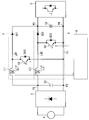
- the switching power supply circuit includes a main circuit 1, a slave circuit 2, input terminals P1 and P2, output terminals P3 and P4, and a power supply line LL.
- the power supply line LL connects the input terminal P2 and the output terminal P4.
- a DC voltage is applied between the input terminals P1 and P2.
- the diode rectifier circuit 3 is connected to the input terminals P1 and P2.
- the diode rectifier circuit 3 rectifies the AC voltage from the AC power source 4 and applies the rectified DC voltage between the input terminals P1 and P2.
- the potential applied to the input terminal P2 is lower than the potential applied to the input terminal P1. It is not essential that the diode rectifier circuit 3 is connected to the input terminals P1 and P2. Any configuration that applies a DC voltage between the input terminals P1 and P2 only needs to be connected to the input terminals P1 and P2.
- a capacitor C2 may be provided between the input terminals P1 and P2.
- the capacitor C2 can reduce current noise.
- the main circuit 1 includes a main power supply line LH1, a main reactor L1, a main diode D11, and a main insulated gate bipolar transistor (hereinafter referred to as a main transistor) S1.
- the main power line LH1 connects the input terminal P1 and the output terminal P3.
- the main reactor L1 and the main diode D11 are provided on the main power supply line LH1.
- Main diode D11 is connected in series with main reactor L1 on the side opposite to input terminal P1 with respect to main reactor L1.
- the anode of the main diode D11 is provided toward the main reactor L1 side.
- the main transistor S1 is provided between a point between the main reactor L1 and the main diode D11 and the power supply line LL.
- the main transistor S1 is provided with its collector terminal facing the main power supply line LH1 and its emitter terminal facing the power supply line LL.
- the main transistor S1 is turned on when a switch signal is input from the control unit 6 to its gate terminal.
- the slave circuit 2 includes a slave power line LH2, a slave reactor L2, slave diodes D21 and D22, and a slave insulated gate bipolar transistor (hereinafter referred to as slave transistor) S2.
- slave transistor a slave insulated gate bipolar transistor
- the slave power line LH2 connects the input terminal P1 and the output terminal P3.
- the sub reactor L2 and the sub diode D21 are provided on the sub power line LH2.
- the inductance of the sub reactor L2 is equal to the inductance of the main reactor L1.
- the sub diode D21 is connected in series with the sub reactor L2 on the side opposite to the input terminal P1 with respect to the sub reactor L2.
- the slave diode D21 has an anode facing the slave reactor L2.
- the sub-transistor S2 is provided between the point between the sub-reactor L2 and the sub-diode D21 and the power supply line LL.
- the sub transistor S2 is provided with its collector terminal facing the sub power line LH2 and its emitter terminal facing the power line LL.
- the sub-transistor S2 is turned on when a switch signal is input from the control unit 6 to its gate terminal.
- the slave diode D22 is connected in parallel with the slave transistor S2 with its anode directed toward the power supply line LL.
- a smoothing capacitor C1 is provided between the output terminals P3 and P4.
- the control unit 6 detects the current IL1 flowing through the main reactor L1, and makes the main transistor S1 conductive based on the current IL1.
- the controller 6 turns on the sub-transistor S2 on the condition that a predetermined period has elapsed since the main transistor S1 was turned on. Further, the control unit 6 may detect the current IL2 flowing through the sub reactor L2, and may make the sub transistor S2 conductive when one of the above conditions and a condition based on the current IL2 are satisfied. These conductions will be described in detail later.
- a method in which each reactor L1 and L2 constitutes a transformer can be adopted as in each document cited in the prior art document. Note that the control of the main transistor S1 and the sub-transistor S2 described below is mainly performed by the control unit 6 unless otherwise specified.
- the control unit 6 includes a microcomputer and a storage device.
- the microcomputer executes each processing step (in other words, a procedure) described in the program.
- the storage device is composed of one or more of various storage devices such as a ROM (Read Only Memory), a RAM (Random Access Memory), a rewritable nonvolatile memory (EPROM (Erasable Programmable ROM), etc.), and a hard disk device, for example. Is possible.
- the storage device stores various information, data, and the like, stores a program executed by the microcomputer, and provides a work area for executing the program. It can be understood that the microcomputer functions as various means corresponding to each processing step described in the program, or can realize that various functions corresponding to each processing step are realized. Further, the control unit 6 is not limited to this, and various procedures executed by the control unit 6 or various means or various functions to be realized may be realized in hardware or in part.
- This switching power supply circuit is suitable for high current applications as compared to, for example, a MOS field effect transistor because the main circuit 1 and the subcircuit 2 are each provided with insulated gate bipolar transistors S1 and S2.
- this switching power supply circuit is used for a large current application, it is desirable to employ a diode having a small forward drop voltage as the main diode D11 and the sub diode D21. This is because the conduction loss in the main diode D11 and the sub diode D21 increases as the current increases.
- the reverse recovery characteristics of the main diode D11 and the slave diode D21 are not excellent, and the reverse recovery current easily flows through the main diode D11 and the slave diode D21.
- the reverse recovery characteristics of the main diode D11 and the sub diode D21 are the same.
- an inverter 5 is connected to the output terminals P3 and P4.
- the inverter 5 does not need to be connected to the output terminals P3 and P4, and any other load may be connected to the output terminals P3 and P4.
- a current flows from the input terminal P1 to the input terminal P2 via the main reactor L1 and the main transistor S1.
- Such a current increases according to a slope determined by the inductance of the main reactor L1 and the DC voltage between the input terminals P1 and P2 (see the current IL1 in FIG. 2). Electromagnetic energy is accumulated in the reactor L1 by such current.
- the main transistor S1 When the main transistor S1 is switched from conduction to non-conduction, current flows from the input terminal P1 to the input terminal P2 via the main reactor L1, the main diode D11, and the smoothing capacitor C1. At this time, the voltage (inductive electromotive voltage) due to the electromagnetic energy accumulated in the reactor L1 is added to the DC voltage between the input terminals P1 and P2, and the sum is applied to the smoothing capacitor C1. Therefore, the main circuit 1 can boost the DC voltage between the input terminals P1 and P2 and apply it to the smoothing capacitor C1.
- Such current is reduced by an inclination based on the inductance of the main reactor L1 and the capacitance of the smoothing capacitor C1 (see current IL1 in FIG. 2).
- the current that is, the current IL1 becomes zero
- the main transistor S1 is turned on again. Thereafter, the above-described operation is repeated. With this operation, the current IL1 changes along a sawtooth shape.
- a mode in which the main transistor S1 is turned on after the current IL1 flowing through the main reactor L1 reaches zero is called a so-called critical current mode.
- the main circuit 1 can function as a switching power supply circuit that boosts the voltage between the input terminals P1 and P2 and applies it between the output terminals P3 and P4. Even in a period in which no current flows to the smoothing capacitor C1 (a period in which the main transistor S1 is conductive), current flows in the diode rectifier circuit 3 via the main transistor S1. Therefore, the conduction angle of the current flowing through the diode rectifier circuit 3 can be expanded. In other words, the main circuit 1 can function as a power factor correction circuit.
- An insulated gate bipolar transistor is employed as the switching element of the main circuit 1. Therefore, for example, a larger current can be passed as compared with a configuration employing a MOS field effect transistor.
- the sub-transistor S2 is turned on under a first condition that a predetermined period has elapsed since the main transistor S1 was turned on.
- the predetermined period is a period shorter than a period (hereinafter also referred to as a cycle) T from when the main transistor S1 is turned on to when it is turned on again.
- a cycle a period (hereinafter also referred to as a cycle) T from when the main transistor S1 is turned on to when it is turned on again.
- the slave circuit 2 performs the same operation with a half cycle delay with respect to the main circuit 1. Therefore, current IL2 flowing through sub reactor L2 is delayed by a half cycle with respect to current IL1 flowing through main reactor L1. Therefore, when one of the currents IL1 and IL2 is small, the other is large.
- the current flowing through the diode rectifier circuit 3 is equal to the current IL1 flowing through the main reactor L1.
- the current flowing through the diode rectifier circuit 3 is equal to the sum of the currents IL1 and IL2.
- the other is large, so that the average value of the current flowing through the diode rectifier circuit 3 can be increased without changing the maximum value (peak) of the current (FIG. 2).
- the peak of the current flowing through the diode rectifier circuit 3 can be reduced in order to achieve the same average current value.
- the sub-transistor S2 may be conducted on the second condition that the current IL2 flowing through the sub-reactor L2 reaches zero. As a result, the operation in the critical current mode can be ensured in the follower circuit 2 more reliably.
- the present switching power supply circuit is devised as follows so that the phase difference returns to the half cycle.
- the phase difference shift will be described.
- the voltage between the input terminals P1 and P2 increases instantaneously, and thereby the current IL2 can be delayed to zero.
- the slave transistor S2 is turned on further later than the time when the main transistor S1 is turned on by a half cycle delay.
- the slave transistor S2 is turned on when three-fifths of the period has elapsed since the time when the main transistor S1 was turned on.
- the currents IL1 and IL2 reach zero at the same period, so that the phase difference between the currents IL1 and IL2 maintains a value corresponding to three-fifth period. Therefore, the conduction time points of the main transistor S1 and the sub transistor S2 are shifted from each other by 3/5 cycles.
- the conduction period t2 of the sub-transistor S2 is set shorter than the conduction period t1 of the main transistor S1 in order to return the phase difference shift to a half cycle.
- the conduction period of the main transistor S1 is set to several microseconds, and the conduction period of the slave transistor S2 is set to be shorter by several hundreds of seconds.
- the peak of the current IL1 is lower than the peak of the current IL2.
- the current IL2 is reduced from a value lower than the current IL1. Moreover, since the inductances of the main reactor L1 and the sub reactor L2 are approximately the same, the inclination when the currents IL1 and IL2 are reduced is also approximately the same. Therefore, the period from when the sub transistor S2 is turned on to when the current IL2 becomes zero is shorter than the period (one cycle T) from when the main transistor S1 becomes conductive until the current IL1 reaches zero. Therefore, the current IL2 reaches zero before one cycle T elapses from the time when the slave transistor S2 becomes conductive.
- the period between the conduction points of the main transistor S ⁇ b> 1 and the slave transistor S ⁇ b> 2 is 3/5 cycles Even when the main transistor S1 and the sub-transistor S2 repeat conduction / non-conduction, the period can be returned to the half cycle.
- the difference between the conduction period t2 and the conduction period t1 may be variable. For example, if the current IL2 has already reached zero when a predetermined period (here, a half cycle) has elapsed since the main transistor S1 was turned on, the difference SUB1 is employed. If the current IL1 has not yet reached zero when a predetermined period has elapsed from when the main transistor S1 is turned on, the difference SUB2 larger than the difference SUB1 is employed.
- a predetermined period here, a half cycle
- the minimum value of the current IL2 is smaller than the minimum value of the current IL1.
- the minimum value of the current IL1 is ⁇ 0.32A
- the minimum value of the current IL2 is ⁇ 0.40A.
- the magnitude relationship between the minimum values of the currents IL1 and IL2 is considered as follows.
- the time point when the currents IL1 and IL2 change from increasing to decreasing depends on the time point when the main transistor S1 and the sub transistor S2 are turned on.
- the main transistor S1 receives a switch signal at its gate terminal when the current IL1 reaches zero, and the slave transistor S2 receives a switch signal at its gate terminal after the current IL2 reaches zero. Therefore, the period from when the current IL2 reaches zero until the current IL2 changes from decrease to increase is longer than the period from when the current IL1 reaches zero until the current IL1 changes from decrease to increase. Therefore, the minimum value of the current IL2 is smaller than the minimum value of the current IL1.
- the minimum value of the current IL1 is smaller than the minimum value of the current IL2, so that the current IL1 decreases from the minimum value to zero. Is shorter than the period until the current IL2 reaches the minimum value to zero. Therefore, the period during which the reverse voltage is applied to the main transistor S1 is shorter than that of the slave transistor S2.
- a slave diode D22 is provided in reverse parallel to the slave transistor S2 to which a reverse voltage can be applied over a long period of time.
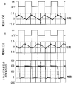
- FIG. 6 shows an example of a timing chart for the present switching power supply circuit.
- the current ID2 that flows through the slave diode D21, the current IL2, the current ISD2 that flows through one set of the slave transistor S2 and the slave diode D22, and the voltage VS2 across the slave transistor S2 are shown at the same coordinates. Yes. In this coordinate, when the vertical axis is regarded as current, the height of one block indicates 5A, and when the vertical axis is regarded as voltage, the height of one block indicates 200V.
- the horizontal axes A, B, and C arranged in order from the top in the figure indicate that the current values of the currents ISD2, IL2, and IS2 are zero, respectively, and the second horizontal axis D from the bottom in the figure indicates the voltage VS2 of the both-ends voltage VS2. It shows that the voltage value is zero.
- the direction from the secondary reactor L2 to the output terminal P3 is positive
- the current ISD2 the direction from the secondary power supply line LH2 to the power supply line LL is positive.
- the matter that the sub-transistor S2 conducts on the condition that the current IL2 reaches zero is one of the conditions. is required.
- the above items are not essential requirements for the reverse voltage applied to the slave transistor S2 due to the reverse recovery current described above. In short, it is only necessary that the inductances of the main reactor L1 and the sub reactor L2 are the same and the conduction period t2 is shorter than the conduction period t1.
- the main circuit 1 may further include a main diode D12.
- the main diode D12 is connected in parallel with the main transistor S1 with the anode directed toward the power supply line LL and the cathode directed toward the main power supply line LH1.
- the reverse voltage applied to the main transistor S1 can also be eliminated by the main diode D12.
- the charge / discharge current due to the parasitic capacitance existing in each part can flow by switching the main transistor S1 from non-conduction to conduction (turn-on) or switching from conduction to non-conduction (turn-off).
- Such charge / discharge current flows not only in the main circuit 1 but also in the sub-circuit 2 and can adversely affect the operation of the sub-circuit 2.
- the charging / discharging current also flows due to the turn-on or turn-off of the sub-transistor S2, which can adversely affect the main circuit 1. Further, under the influence of the charge / discharge current, there is a possibility of failing to detect that the currents IL1 and IL2 have become zero.
- the capacitance of the capacitor C2 be 0.5 ⁇ F or more. As a result, the charge / discharge current can be reduced. As a result, the adverse effect of the main circuit 1 and the subcircuit 2 acting on each other and the failure of the zero current detection of the currents IL1 and IL2 can be avoided or suppressed.
- the switching power supply circuit includes one main circuit 1 and one sub circuit 2. However, a plurality of slave circuits 2 may be provided. If the switching power supply circuit includes two slave circuits 2, one slave circuit 2 operates with a delay of a first predetermined period (for example, one-third cycle) with respect to the main circuit 1, and the other slave circuit 2 2 operates with a delay of a second predetermined period (for example, two-thirds cycle) with respect to the main circuit 1.
- a first predetermined period for example, one-third cycle
- a second predetermined period for example, two-thirds cycle
Abstract
Description
<構成>
図1に例示するように、本スイッチング電源回路は主回路1と従回路2と入力端P1,P2と出力端P3,P4と電源線LLとを備えている。電源線LLは入力端P2と出力端P4とを接続している。
まず図1,2を参照して本スイッチング電源回路の動作の概要について説明する。なお以下の説明及び図面では、電流IL1,IL2についてダイオード整流回路3からインバータ5側へ向かう方向を正と仮定している。
2 従回路
C2 コンデンサ
D11,D12,D21,D22 ダイオード
L1,L2 リアクトル
LH1,LH2,LL 電源線
S1,S2 絶縁ゲートバイポーラトランジスタ
Claims (5)
- 低電源線(LL)と、
いずれも前記低電源線よりも高い電位が印加される主電源線及び従電源線(LH1,LH2)と、
前記主電源線及び前記従電源線の上にそれぞれ設けられ、互いに等しいインダクタンスを有する主リアクトル及び従リアクトル(L1、L2)と、
前記主電源線及び前記従電源線の上でそれぞれ前記主リアクトル及び前記従リアクトルと直列に接続され、アノードをそれぞれ前記主リアクトル及び前記従リアクトル側に向けて設けられた第1の主ダイオード及び第1の従ダイオード(D11,D21)と、
前記主リアクトルと前記主ダイオードとの間の点と、前記低電源線との間で、エミッタを前記低電源線に向けて設けられ、前記主リアクトルを流れる電流が零に至ることを以って導通し、第1期間(t1)経過後に非導通する主絶縁ゲートバイポーラトランジスタ(S1)と、
前記従リアクトルと前記従ダイオードとの間の点と、前記低電源線との間で、エミッタを前記低電源線に向けて設けられ、前記主絶縁ゲートバイポーラトランジスタが導通した時点から、次に導通するまでの期間よりも短い一定期間を経過したことを条件の一つとして導通し、前記第1期間よりも短い第2期間(t2)経過後に非導通する従絶縁ゲートバイポーラトランジスタ(S1)と、
前記従絶縁ゲートバイポーラトランジスタ(S2)と並列に接続され、アノードを前記前記低電源線に向けて設けられた第2の従ダイオード(D22)と
を備える、スイッチング電源回路。 - 前記主絶縁ゲートバイポーラトランジスタ(S1)と並列に接続され、アノードを前記主電源線(LH1)に向けて設けられた第2の主ダイオード(D12)を更に有する、請求項1に記載のスイッチング電源回路。
- 一端が前記低電位線(LL)と、他端が、前記主リアクトル(L1)に対して前記第1の主ダイオード(D11)とは反対側で前記主電源線(LH1)と、前記従リアクトル(L2)に対して前記第1の従ダイオード(D21)とは反対側で前記従電源線(LH2)とに共通して接続され、静電容量が0.5μF以上であるコンデンサ(C2)を更に備える、請求項1又は2に記載のスイッチング電源回路。
- 前記条件と、前記従リアクトル(L2)を流れる電流が零に至る第2条件との両方を満足するときに前記従絶縁ゲートバイポーラトランジスタ(S2)を導通させる、請求項1又は2に記載のスイッチング電源回路。
- 前記条件と、前記従リアクトル(L2)を流れる電流が零に至る第2条件との両方を満足するときに前記従絶縁ゲートバイポーラトランジスタ(S2)を導通させる、請求項3に記載のスイッチング電源回路。
Priority Applications (5)
| Application Number | Priority Date | Filing Date | Title |
|---|---|---|---|
| ES10829852T ES2875422T3 (es) | 2009-11-12 | 2010-10-29 | Circuito de alimentación de conmutación |
| US13/498,596 US8952667B2 (en) | 2009-11-12 | 2010-10-29 | Switching power supply circuit |
| EP10829852.2A EP2501027B1 (en) | 2009-11-12 | 2010-10-29 | Switching power supply circuit |
| CN201080051217.5A CN102640407B (zh) | 2009-11-12 | 2010-10-29 | 开关电源电路 |
| AU2010319195A AU2010319195B2 (en) | 2009-11-12 | 2010-10-29 | Switching power supply circuit |
Applications Claiming Priority (2)
| Application Number | Priority Date | Filing Date | Title |
|---|---|---|---|
| JP2009-258565 | 2009-11-12 | ||
| JP2009258565A JP4853568B2 (ja) | 2009-11-12 | 2009-11-12 | スイッチング電源回路 |
Publications (1)
| Publication Number | Publication Date |
|---|---|
| WO2011058892A1 true WO2011058892A1 (ja) | 2011-05-19 |
Family
ID=43991551
Family Applications (1)
| Application Number | Title | Priority Date | Filing Date |
|---|---|---|---|
| PCT/JP2010/069305 WO2011058892A1 (ja) | 2009-11-12 | 2010-10-29 | スイッチング電源回路 |
Country Status (7)
| Country | Link |
|---|---|
| US (1) | US8952667B2 (ja) |
| EP (1) | EP2501027B1 (ja) |
| JP (1) | JP4853568B2 (ja) |
| CN (1) | CN102640407B (ja) |
| AU (1) | AU2010319195B2 (ja) |
| ES (1) | ES2875422T3 (ja) |
| WO (1) | WO2011058892A1 (ja) |
Families Citing this family (16)
| Publication number | Priority date | Publication date | Assignee | Title |
|---|---|---|---|---|
| EP2341605B1 (en) * | 2009-12-31 | 2018-03-07 | Nxp B.V. | A power factor correction stage |
| US8912775B2 (en) * | 2011-04-12 | 2014-12-16 | Infineon Technologies Ag | Power factor correction circuit having multiple switched-mode converter circuits |
| JP5584826B2 (ja) | 2011-04-26 | 2014-09-03 | ルネサスエレクトロニクス株式会社 | Pfc信号生成回路、それを用いたpfc制御システム、及びpfc制御方法 |
| CN104641543B (zh) * | 2012-09-21 | 2016-04-27 | 大金工业株式会社 | 直接型电力变换装置的控制方法 |
| KR101420516B1 (ko) * | 2012-10-30 | 2014-07-16 | 삼성전기주식회사 | 역률 개선 회로 및 역률 개선 제어 방법 |
| KR101412821B1 (ko) * | 2012-10-31 | 2014-06-27 | 삼성전기주식회사 | 역률 보정 회로 및 이를 포함하는 전원 장치 |
| KR101496810B1 (ko) | 2012-12-05 | 2015-02-27 | 삼성전기주식회사 | 역률 보정 장치, 전원 장치 및 모터 구동 장치 |
| EP2985897B1 (en) * | 2013-04-12 | 2019-10-02 | Mitsubishi Electric Corporation | Power conversion device |
| WO2015001617A1 (ja) * | 2013-07-02 | 2015-01-08 | 三菱電機株式会社 | 逆流防止装置、電力変換装置、モータ駆動装置及び冷凍空気調和装置 |
| JP5794273B2 (ja) * | 2013-10-07 | 2015-10-14 | ダイキン工業株式会社 | 直接形電力変換装置の制御方法 |
| CN104167918B (zh) * | 2014-06-30 | 2017-06-13 | 阳光电源股份有限公司 | 一种高变压比的直流‑直流变换器 |
| JP5930108B2 (ja) * | 2014-09-25 | 2016-06-08 | ダイキン工業株式会社 | 電力変換装置 |
| WO2017091998A1 (en) | 2015-12-03 | 2017-06-08 | Abb Beijing Drive Systems Co., Ltd. | Chopper assembly and controlling method thereof |
| WO2018038362A1 (ko) * | 2016-08-22 | 2018-03-01 | 데스틴파워 주식회사 | 벅 부스트 컨버터 |
| US10291111B1 (en) * | 2018-03-23 | 2019-05-14 | Hamilton Sundstrand Corporation | Feedback control for parallel power converter synchronization |
| JP2021058039A (ja) * | 2019-10-01 | 2021-04-08 | シャープ株式会社 | 整流回路および電源装置 |
Citations (2)
| Publication number | Priority date | Publication date | Assignee | Title |
|---|---|---|---|---|
| JP2006223025A (ja) * | 2005-02-08 | 2006-08-24 | Honda Motor Co Ltd | Dc/dcコンバータ |
| JP2007195282A (ja) * | 2006-01-17 | 2007-08-02 | Renesas Technology Corp | 電源装置 |
Family Cites Families (7)
| Publication number | Priority date | Publication date | Assignee | Title |
|---|---|---|---|---|
| US6091233A (en) * | 1999-01-14 | 2000-07-18 | Micro Linear Corporation | Interleaved zero current switching in a power factor correction boost converter |
| JP4098299B2 (ja) * | 2004-11-18 | 2008-06-11 | 本田技研工業株式会社 | Dc/dcコンバータ |
| US7304461B2 (en) | 2004-11-18 | 2007-12-04 | Honda Motor Co., Ltd. | DC/DC converter |
| JP2007252177A (ja) | 2006-02-20 | 2007-09-27 | Toshiba Kyaria Kk | 電力変換装置 |
| JP4963068B2 (ja) | 2007-02-06 | 2012-06-27 | 新電元工業株式会社 | 力率改善回路 |
| JP2009159727A (ja) * | 2007-12-26 | 2009-07-16 | Toshiba Corp | コンバータ電源回路およびコンバータ電源駆動方法 |
| JP5085397B2 (ja) * | 2008-04-11 | 2012-11-28 | ルネサスエレクトロニクス株式会社 | 電源装置および半導体集積回路装置 |
-
2009
- 2009-11-12 JP JP2009258565A patent/JP4853568B2/ja not_active Expired - Fee Related
-
2010
- 2010-10-29 ES ES10829852T patent/ES2875422T3/es active Active
- 2010-10-29 EP EP10829852.2A patent/EP2501027B1/en active Active
- 2010-10-29 US US13/498,596 patent/US8952667B2/en active Active
- 2010-10-29 WO PCT/JP2010/069305 patent/WO2011058892A1/ja active Application Filing
- 2010-10-29 CN CN201080051217.5A patent/CN102640407B/zh active Active
- 2010-10-29 AU AU2010319195A patent/AU2010319195B2/en active Active
Patent Citations (2)
| Publication number | Priority date | Publication date | Assignee | Title |
|---|---|---|---|---|
| JP2006223025A (ja) * | 2005-02-08 | 2006-08-24 | Honda Motor Co Ltd | Dc/dcコンバータ |
| JP2007195282A (ja) * | 2006-01-17 | 2007-08-02 | Renesas Technology Corp | 電源装置 |
Non-Patent Citations (2)
| Title |
|---|
| MAMORU KITAMURA: "1.5kW no Tei-noise Ko-choha Taisaku Dengen o Tsukureru Rinkai Mode/ Interleave PFC IC R2A20112", TRANSISTOR GIJUTSU, May 2008 (2008-05-01), pages 176 - 184, XP008160209 * |
| See also references of EP2501027A4 * |
Also Published As
| Publication number | Publication date |
|---|---|
| AU2010319195B2 (en) | 2014-02-06 |
| AU2010319195A1 (en) | 2012-04-26 |
| EP2501027A4 (en) | 2017-10-18 |
| JP2011103753A (ja) | 2011-05-26 |
| US20120187929A1 (en) | 2012-07-26 |
| EP2501027A1 (en) | 2012-09-19 |
| JP4853568B2 (ja) | 2012-01-11 |
| CN102640407B (zh) | 2015-01-21 |
| ES2875422T3 (es) | 2021-11-10 |
| US8952667B2 (en) | 2015-02-10 |
| CN102640407A (zh) | 2012-08-15 |
| EP2501027B1 (en) | 2021-06-09 |
Similar Documents
| Publication | Publication Date | Title |
|---|---|---|
| JP4853568B2 (ja) | スイッチング電源回路 | |
| US8724348B2 (en) | Power-supply unit, hard-disk drive, and switching method of the power-supply unit | |
| JP5590124B2 (ja) | Dc−dcコンバータ | |
| AU2013342516B2 (en) | Switching Power Supply Circuit Control Method | |
| US20150002108A1 (en) | Bridgeless power factor correction boost converter | |
| AU2011230323A1 (en) | Switching power supply circuit, and method for control of switching power supply circuit | |
| JPWO2012176403A1 (ja) | 昇降圧型ac/dcコンバータ | |
| WO2018061286A1 (ja) | 電力変換装置 | |
| CN112134474A (zh) | 半导体装置 | |
| JP5482358B2 (ja) | スイッチング電源回路の制御方法 | |
| KR20190064962A (ko) | Dc-dc 변환 시스템 | |
| US20200067413A1 (en) | Dc/dc converter | |
| JP5987423B2 (ja) | 電力変換装置 | |
| JP6458235B2 (ja) | スイッチング電源装置 | |
| WO2015178106A1 (ja) | 電源装置 | |
| JP5578234B2 (ja) | スイッチング電源装置およびこれを用いた電源システム、電子装置 | |
| WO2021028990A1 (ja) | Dc-dcコンバータ | |
| JP2013110785A (ja) | 三相整流装置 | |
| JP6052221B2 (ja) | 電力変換装置 | |
| JP6191017B2 (ja) | ハーフブリッジ回路及びハーフブリッジ回路から構成されるフルブリッジ回路及び3相インバータ回路 | |
| WO2024043124A1 (ja) | 電力変換装置 | |
| US9312749B2 (en) | Driver device for power factor correction circuit | |
| JP2018093610A (ja) | 電力変換回路 | |
| JP2020022299A (ja) | 電源装置 | |
| JP2014200173A (ja) | Dc−dcコンバータ |
Legal Events
| Date | Code | Title | Description |
|---|---|---|---|
| WWE | Wipo information: entry into national phase |
Ref document number: 201080051217.5 Country of ref document: CN |
|
| 121 | Ep: the epo has been informed by wipo that ep was designated in this application |
Ref document number: 10829852 Country of ref document: EP Kind code of ref document: A1 |
|
| WWE | Wipo information: entry into national phase |
Ref document number: 684/KOLNP/2012 Country of ref document: IN |
|
| WWE | Wipo information: entry into national phase |
Ref document number: 2010829852 Country of ref document: EP |
|
| WWE | Wipo information: entry into national phase |
Ref document number: 13498596 Country of ref document: US |
|
| WWE | Wipo information: entry into national phase |
Ref document number: 2010319195 Country of ref document: AU |
|
| ENP | Entry into the national phase |
Ref document number: 2010319195 Country of ref document: AU Date of ref document: 20101029 Kind code of ref document: A |
|
| NENP | Non-entry into the national phase |
Ref country code: DE |