WO2011036717A1 - 化合物薄膜太陽電池 - Google Patents
化合物薄膜太陽電池 Download PDFInfo
- Publication number
- WO2011036717A1 WO2011036717A1 PCT/JP2009/004842 JP2009004842W WO2011036717A1 WO 2011036717 A1 WO2011036717 A1 WO 2011036717A1 JP 2009004842 W JP2009004842 W JP 2009004842W WO 2011036717 A1 WO2011036717 A1 WO 2011036717A1
- Authority
- WO
- WIPO (PCT)
- Prior art keywords
- thin film
- layer
- solar cell
- light absorption
- aforementioned
- Prior art date
- Legal status (The legal status is an assumption and is not a legal conclusion. Google has not performed a legal analysis and makes no representation as to the accuracy of the status listed.)
- Ceased
Links
Images

Classifications
-
- H—ELECTRICITY
- H10—SEMICONDUCTOR DEVICES; ELECTRIC SOLID-STATE DEVICES NOT OTHERWISE PROVIDED FOR
- H10F—INORGANIC SEMICONDUCTOR DEVICES SENSITIVE TO INFRARED RADIATION, LIGHT, ELECTROMAGNETIC RADIATION OF SHORTER WAVELENGTH OR CORPUSCULAR RADIATION
- H10F77/00—Constructional details of devices covered by this subclass
- H10F77/10—Semiconductor bodies
- H10F77/12—Active materials
- H10F77/126—Active materials comprising only Group I-III-VI chalcopyrite materials, e.g. CuInSe2, CuGaSe2 or CuInGaSe2 [CIGS]
-
- H—ELECTRICITY
- H10—SEMICONDUCTOR DEVICES; ELECTRIC SOLID-STATE DEVICES NOT OTHERWISE PROVIDED FOR
- H10F—INORGANIC SEMICONDUCTOR DEVICES SENSITIVE TO INFRARED RADIATION, LIGHT, ELECTROMAGNETIC RADIATION OF SHORTER WAVELENGTH OR CORPUSCULAR RADIATION
- H10F10/00—Individual photovoltaic cells, e.g. solar cells
- H10F10/10—Individual photovoltaic cells, e.g. solar cells having potential barriers
- H10F10/16—Photovoltaic cells having only PN heterojunction potential barriers
- H10F10/167—Photovoltaic cells having only PN heterojunction potential barriers comprising Group I-III-VI materials, e.g. CdS/CuInSe2 [CIS] heterojunction photovoltaic cells
-
- H—ELECTRICITY
- H10—SEMICONDUCTOR DEVICES; ELECTRIC SOLID-STATE DEVICES NOT OTHERWISE PROVIDED FOR
- H10P—GENERIC PROCESSES OR APPARATUS FOR THE MANUFACTURE OR TREATMENT OF DEVICES COVERED BY CLASS H10
- H10P14/00—Formation of materials, e.g. in the shape of layers or pillars
- H10P14/20—Formation of materials, e.g. in the shape of layers or pillars of semiconductor materials
- H10P14/29—Formation of materials, e.g. in the shape of layers or pillars of semiconductor materials characterised by the substrates
- H10P14/2901—Materials
- H10P14/2922—Materials being non-crystalline insulating materials, e.g. glass or polymers
-
- H—ELECTRICITY
- H10—SEMICONDUCTOR DEVICES; ELECTRIC SOLID-STATE DEVICES NOT OTHERWISE PROVIDED FOR
- H10P—GENERIC PROCESSES OR APPARATUS FOR THE MANUFACTURE OR TREATMENT OF DEVICES COVERED BY CLASS H10
- H10P14/00—Formation of materials, e.g. in the shape of layers or pillars
- H10P14/20—Formation of materials, e.g. in the shape of layers or pillars of semiconductor materials
- H10P14/32—Formation of materials, e.g. in the shape of layers or pillars of semiconductor materials characterised by intermediate layers between substrates and deposited layers
- H10P14/3202—Materials thereof
- H10P14/3241—Materials thereof being conductive materials
-
- H—ELECTRICITY
- H10—SEMICONDUCTOR DEVICES; ELECTRIC SOLID-STATE DEVICES NOT OTHERWISE PROVIDED FOR
- H10P—GENERIC PROCESSES OR APPARATUS FOR THE MANUFACTURE OR TREATMENT OF DEVICES COVERED BY CLASS H10
- H10P14/00—Formation of materials, e.g. in the shape of layers or pillars
- H10P14/20—Formation of materials, e.g. in the shape of layers or pillars of semiconductor materials
- H10P14/34—Deposited materials, e.g. layers
- H10P14/3402—Deposited materials, e.g. layers characterised by the chemical composition
- H10P14/3434—Deposited materials, e.g. layers characterised by the chemical composition being oxide semiconductor materials
-
- H—ELECTRICITY
- H10—SEMICONDUCTOR DEVICES; ELECTRIC SOLID-STATE DEVICES NOT OTHERWISE PROVIDED FOR
- H10P—GENERIC PROCESSES OR APPARATUS FOR THE MANUFACTURE OR TREATMENT OF DEVICES COVERED BY CLASS H10
- H10P14/00—Formation of materials, e.g. in the shape of layers or pillars
- H10P14/20—Formation of materials, e.g. in the shape of layers or pillars of semiconductor materials
- H10P14/34—Deposited materials, e.g. layers
- H10P14/3402—Deposited materials, e.g. layers characterised by the chemical composition
- H10P14/3436—Deposited materials, e.g. layers characterised by the chemical composition being chalcogenide semiconductor materials not being oxides, e.g. ternary compounds
-
- H—ELECTRICITY
- H10—SEMICONDUCTOR DEVICES; ELECTRIC SOLID-STATE DEVICES NOT OTHERWISE PROVIDED FOR
- H10P—GENERIC PROCESSES OR APPARATUS FOR THE MANUFACTURE OR TREATMENT OF DEVICES COVERED BY CLASS H10
- H10P14/00—Formation of materials, e.g. in the shape of layers or pillars
- H10P14/20—Formation of materials, e.g. in the shape of layers or pillars of semiconductor materials
- H10P14/38—Formation of materials, e.g. in the shape of layers or pillars of semiconductor materials characterised by treatments done after the formation of the materials
-
- Y—GENERAL TAGGING OF NEW TECHNOLOGICAL DEVELOPMENTS; GENERAL TAGGING OF CROSS-SECTIONAL TECHNOLOGIES SPANNING OVER SEVERAL SECTIONS OF THE IPC; TECHNICAL SUBJECTS COVERED BY FORMER USPC CROSS-REFERENCE ART COLLECTIONS [XRACs] AND DIGESTS
- Y02—TECHNOLOGIES OR APPLICATIONS FOR MITIGATION OR ADAPTATION AGAINST CLIMATE CHANGE
- Y02E—REDUCTION OF GREENHOUSE GAS [GHG] EMISSIONS, RELATED TO ENERGY GENERATION, TRANSMISSION OR DISTRIBUTION
- Y02E10/00—Energy generation through renewable energy sources
- Y02E10/50—Photovoltaic [PV] energy
- Y02E10/541—CuInSe2 material PV cells
Definitions
- the present invention relates to a compound thin film solar cell.
- I-III-VI 2 based compound semiconductor having a chalcopyrite structure is mainly composed of Cu as a group I element, In and / or Ga as a group III element, and Se and / or S as a group VI element.
- a group I element In and / or Ga
- Se and / or S as a group VI element
- a compound thin film solar cell using Cu (In 1-x Ga x ) (Se 1-y S y ) 2 for the light absorption layer contains In and Ga as constituent elements.
- In and Ga are rare metals, and there is a high possibility that stable supply will be difficult due to the fact that it is difficult to produce high-grade ores that have low resource reserves or that can be mined economically.
- refining from ore is not easy because refining requires very high technology and large energy, and this is a factor that increases the price.
- a highly efficient CIGS (Cu (In 1-x Ga x ) Se 2 ) solar cell is obtained with a thin film of a p-type semiconductor in which CIGS has a slight Group III excess composition from a constant ratio.
- a multi-source deposition method particularly a three-stage method is used.
- In, Ga, Se is vapor-deposited on the first layer to form an (In, Ga) 2 Se 3 film, and then only Cu and Se are supplied to make the composition of the entire film Cu-rich.
- In, Ga, and Se fluxes are supplied again to make the final composition of the film (In, Ga) excessive.
- the vapor deposition method can precisely control the chemical composition and can produce a highly efficient CIGS solar cell, but it is difficult to increase the area due to process limitations.
- the compound thin film solar cell uses CuIn x Ga 1-x Se 2 (CIGS) (solid solution of CuInSe 2 and CuGaSe 2 ) or CdTe as a light absorption layer, and both are made of a material containing a harmful metal or a rare metal. Therefore, there is a problem that the environmental load is large and the manufacturing cost of the solar cell is increased.
- CGS CuIn x Ga 1-x Se 2
- the present invention aims to solve such a problem, and a compound thin film having a material structure that does not contain a harmful element typified by Se or Cd and a rare element typified by In or Ga as much as possible while maintaining high conversion efficiency. It aims at providing a solar cell and its manufacturing method.
- the compound thin film solar cell includes a substrate, a back electrode provided on the substrate, a take-out electrode provided on the back electrode, a light absorption layer provided on the back electrode, and the light absorption layer.
- a buffer layer provided; a transparent electrode layer provided on the buffer layer; an antireflection film provided on the transparent electrode layer; and a take-out electrode provided on the transparent electrode layer.
- a compound thin film solar cell having a material configuration that contains as little a harmful element as typified by Se or Cd and a rare element typified by In or Ga as much as possible.
- Se is used as a group VI element in a chalcopyrite compound semiconductor of the I-III-VI 2 system.
- Se has strong toxicity and a large band gap, there are environmental problems and cost problems such as the need to use a large amount of rare metals such as Ga and In. Te is less toxic than Se, and has a preferable characteristic that the band gap is small and the amount of rare metal used can be reduced as compared with a chalcopyrite compound semiconductor using Se as a group VI.
- CuAlTe 2 , CuGaTe 2 and CuInTe 2 all exhibit a chalcopyrite structure and form a solid solution.
- Table 1 shows band gaps of chalcopyrite type compound semiconductors of the I-III-VI 2 system and the group VI element consisting of Te.
- CuAlTe 2 in Table 1 is an experimental value obtained by the inventors, and values of CuGaTe 2 and CuInTe 2 are experimental values in the literature.
- the band gap can be greatly modulated by changing only the group III element in the I-III-VI 2 system.
- a preferred band gap for the solar spectrum is 1.0 eV to 1.5 eV.
- the band gap of the optimal sunlight spectrum is often set to 1.4 eV to 1.5 eV. There is also a report that the conversion efficiency becomes maximum in the vicinity of 1.2 eV.
- the band gap is preferably in the range of 1.0 eV to 1.5 eV, which is a preferable band gap for the light absorption layer of the solar cell.
- the band gap is preferably in the range of 1.0 eV to 1.5 eV, which is a preferable band gap for the light absorption layer of the solar cell.
- the band gap is preferably in the range of 1.0 eV to 1.5 eV, which is a preferable band gap for the light absorption layer of the solar cell.
- Compound semiconductor in which group VI Te of the I-III-VI 2 system chalcopyrite compound semiconductor which is a light absorption layer is partially substituted with Se or S (the amount of Se, S is from the amount (mol) of Te) Can be used as the light absorption layer. At that time, it is desired that the chalcopyrite structure is maintained that the band gap is in the range of 1.0 to 1.5 eV.
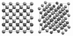
- FIG. 1 illustrates a molecular structure in which part of Te in a chalcopyrite type compound semiconductor CuAlTe 2 is replaced with O.
- the optical band gap of the CuAlTe 2 thin film is 2.25 eV, and the band gap can be controlled to 1.0 eV by replacing Al with In or Ga.
- Te has a lower vapor pressure than Se, it is easy to handle, and it is expected that the composition can be easily controlled when the film is formed. Furthermore, when a Te-based chalcopyrite compound semiconductor is used for the parent phase, the amount of In or Ga added to adjust to the optimum band gap can be reduced, so that segregation can be suppressed and a thin film having a uniform composition can be produced. .
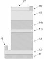
- FIG. 3 shows a schematic cross-sectional view of an example of a compound thin film solar cell according to the present invention.
- the compound thin film solar cell includes a substrate 11, a back electrode 12, a light absorption layer 13, buffer layers 14 a and b, a transparent electrode layer 15, a takeout electrode 16, and an antireflection film 17.
- the substrate 11 it is desirable to use blue plate glass, and it is also possible to use a metal plate such as stainless steel, Ti or Cr, or a resin such as polyimide.
- a metal film such as W can be used. Among these, it is desirable to use a Mo film.
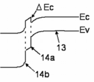
- FIG. 4 shows the band structure of the pn junction interface in the compound thin film solar cell.
- the chalcopyrite compound semiconductor of the light absorption layer 13 is a p-type semiconductor
- the buffer layer 14a typified by CdS or ZnO: Mg functions as an n-type semiconductor
- the buffer layer 14b typified by ZnO functions as an n + -type layer. Conceivable.
- the conduction band discontinuity (CBO) ⁇ E c is preferably 0 eV or more and 0.4 eV or less, and more preferably 0.1 eV or more and 0.35 eV or less.
- the conduction band structure or conduction band discontinuity can be directly evaluated by inverse photoelectron spectroscopy, which is the reverse process of photoemission.
- the thickness of the window layer and buffer layer formed on the light absorption layer is quite thick, such as several ⁇ m and several tens of nm, respectively. In this case, it is necessary to remove each layer without damage or deterioration, and etching using a low ion beam is usually used.
- the transparent electrode layer 15 is required to transmit sunlight and to have conductivity.
- B from ZnO: Al or diborane containing 2 wt% of alumina (Al 2 O 3 ) is used as a dopant.
- ZnO: B can be used.
- the extraction electrode 16 for example, Al, Ag, or Au can be used.
- MgF 2 is desirably used as the antireflection film 17.
- Example 1 A blue glass substrate was used as the substrate 11, and a Mo thin film serving as the back electrode 12 was deposited by about 700 nm by sputtering. Sputtering was performed by applying RF 200 W in an Ar gas atmosphere using Mo as a target. After the Mo thin film to be the back electrode 12 was deposited, a Cu (Al 1-y In y ) Te 2 thin film to be the light absorption layer 13 was similarly deposited by about 2 ⁇ m by RF sputtering. Here, the target composition y was set to 0.8 so that the band gap was about 1.18 eV. Film formation was performed by applying RF 200 W in an Ar gas atmosphere.
- the Cu (Al 1-y In y ) Te 2 thin film immediately after sputter deposition is amorphous and has a very small particle size, but is crystallized by heat treatment at a high temperature, and the particle size becomes 100 nm or more. This can contribute to higher efficiency of solar cells.
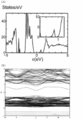
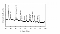
- FIG. 5 is an X-ray diffraction result of a thin film in which CuAlTe 2 serving as a parent phase is deposited under the same conditions as the film forming conditions. It can be seen that the thin film to be the light absorption layer 13 manufactured under the film forming conditions is a single phase film having a chalcopyrite structure. It was estimated from the optical property evaluation of the produced CuAlTe 2 thin film that the optical band gap was 2.25 eV (FIG. 6).
- a ZnO thin film to which Mg was added as a buffer layer 14a was deposited to a thickness of about 50 nm. As shown in FIG. 4, the amount of Mg added was set to 20% so as to form a band offset at the interface between the light absorption layer 13 and the buffer layer 14a. RF sputter was used for film formation, but the output was 50 W in consideration of plasma damage at the interface.
- a ZnO thin film was deposited as a buffer layer 14b, and then ZnO: Al containing 2 wt% of alumina (Al 2 O 3 ) to be the transparent electrode 15 was deposited to about 1 ⁇ m.
- NiCr and Au were deposited by an evaporation method.
- the film thickness was 100 nm and 300 nm, respectively.
- MgF 2 was deposited as an antireflection film 17 to a thickness of about 500 nm by sputtering to produce the compound thin film solar cell shown in FIG.
- Example 2 A blue glass substrate was used as the substrate 11, and a Mo thin film serving as the back electrode 12 was deposited by about 700 nm by sputtering. Sputtering was performed by applying RF 200 W in an Ar gas atmosphere using Mo as a target. After the Mo thin film serving as the back electrode 12 was deposited, a CuAlTe 2 thin film serving as the light absorption layer 13 was similarly deposited by about 2 ⁇ m by RF sputtering. Film formation was performed by applying RF 200 W in an Ar gas atmosphere.
- the film formation chamber was evacuated, and heat treatment was performed in an ultrahigh vacuum atmosphere at 500 ° C.
- the CuAlTe 2 thin film immediately after sputter deposition is amorphous and has a very small particle size, but is crystallized by heat treatment at a high temperature to have a particle size of 100 nm or more.
- Oxygen is ion-implanted into the prepared CuAlTe 2 thin film with an energy of 90 keV, and then recrystallization is performed with an excimer laser annealing to compensate for defects caused by the ion implantation. Replacement was performed.
- a ZnO thin film to which Mg was added as a buffer layer 14a was deposited to a thickness of about 50 nm.
- the amount of Mg added was set to 40% so as to form a band offset at the interface between the light absorption layer 13 and the buffer layer 14a.
- RF sputter was used for film formation, but the output was 50 W in consideration of plasma damage at the interface.
- a ZnO thin film was deposited as a buffer layer 14b, and then ZnO: Al containing 2 wt% of alumina (Al 2 O 3 ) to be the transparent electrode 15 was deposited to about 1 ⁇ m.
- NiCr and Au were deposited by an evaporation method.
- the film thickness was 100 nm and 300 nm, respectively.
- MgF 2 was deposited as an antireflection film 17 to a thickness of about 500 nm by sputtering to produce the compound thin film solar cell shown in FIG.
Landscapes
- Photovoltaic Devices (AREA)
Abstract
Description
(数式1)Eg=2.25-1.02x-1.29y (1.5≧Eg≧1.0)
(数式2)Eg=2.25-1.02x-1.29y (2.25≧Eg≧1.0)
従来はI-III-VI2系のカルコパイライト型化合物半導体において、VI族元素にSeを用いている。しかし、Seには強い毒性があること、バンドギャップが大きくなることから、希少金属であるGaやInを多く用いる必要があることといった、環境問題やコストの問題がある。
TeはSeより毒性が低く、SeをVI族に用いたカルコパイライト型化合物半導体に比べてバンドギャップが小さく希少金属の使用量を少なくできるという好ましい特性がある。
表1にI-III-VI2系でVI族元素がTeから成るカルコパイライト型化合物半導体のバンドギャップを示す。表1のCuAlTe2は発明者らの実験値でCuGaTe2とCuInTe2の値は文献の実験値である。表1から明らかなようにI-III-VI2系でIII族元素のみを変化させることでバンドギャップを大きく変調させることができる。
太陽光スペクトルに好ましいバンドギャップとしては1.0eVから1.5eVである。最適な太陽光スペクトルのバンドギャップとしては1.4eVから1.5eVとされることが多い。1.2eV近傍で変換効率が最大になるという報告もある。

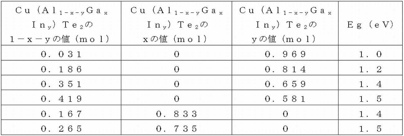
CuAlTe2のAlの一部をInで置換した場合(Cu(Al1-yIny)Te2)では太陽電池の光吸収層として好ましいバンドギャップである1.0eVから1.5eVの範囲とするためには、0.58≦y≦0.97の条件を満たす組成で固溶体を作製することが望まれる。
光吸収層であるI-III-VI2系カルコパイライト型化合物半導体のVI族のTeを一部Se又はSで部分的に置換した化合物半導体(Se、Sの量はTeの量(mol)より少ない)を光吸収層として用いることもできる。その際、バンドギャップが1.0から1.5eVの範囲内にあることカルコパイライト構造を保持していることが望まれる。
CuAlTe2薄膜の光学バンドギャップは2.25eVであり、AlをInあるいはGaで置換することにより、バンドギャップを1.0eVまで制御できる。種々のバンドギャップをもついずれの母相に対しても、中間準位を形成することにより、長波長側の光も取り込むことができ、太陽電池の高効率化が期待される。
基板11としては、青板ガラスを用いることが望ましく、ステンレス、Ti又はCr等の金属板あるいはポリイミド等の樹脂を用いることもできる。
裏面電極としては、W等の金属膜を用いることができる。その中でも、Mo膜を用いることが望ましい。
取り出し電極16としては、例えば、Al、Ag或いはAuを用いることができる。さらに、透明電極15との密着性を向上させるために、Ni或いはCrを堆積させた後、Al、Ag或いはAuを堆積させてもよい。
反射防止膜17としては、例えば、MgF2を用いることが望ましい。
以下、本発明の実施例を詳細に説明する。
基板11として青板ガラス基板を用い、スパッタ法により裏面電極12となるMo薄膜を700nm程度堆積した。スパッタは、Moをタ-ゲットとし、Arガス雰囲気中でRF200W印加することにより行った。
裏面電極12となるMo薄膜堆積後、光吸収層13となるCu(Al1-yIny)Te2薄膜を同じくRFスパッタにより2μm程度堆積した。ここでバンドギャップが1.18eV程度になるように、タ-ゲットの仕込み組成のyを0.8にした。製膜はArガス雰囲気中でRF200W印加することにより行った。
基板11として青板ガラス基板を用い、スパッタ法により裏面電極12となるMo薄膜を700nm程度堆積した。スパッタは、Moをタ-ゲットとし、Arガス雰囲気中でRF200W印加することにより行った。
裏面電極12となるMo薄膜堆積後、光吸収層13となるCuAlTe2薄膜を同じくRFスパッタにより2μm程度堆積した。製膜はArガス雰囲気中でRF200W印加することにより行った。
作製したCuAlTe2薄膜に90keVのエネルギ-で酸素をイオン注入し、その後、イオン注入によりできた欠陥を補償するために、エキシマレ-ザ-アニ-ルにより再結晶化を行い、TeのOによる部分置換を行った。
Claims (5)
- 基板と、
前記基板上に設けられた裏面電極と、
前記裏面電極上に設けられた取り出し電極と、
前記裏面電極上に設けられた光吸収層と、
前記光吸収層上に設けられたバッファ-層と、
前記バッファー層上に設けられた透明電極層と、
前記透明電極層上に設けられた反射防止膜と、
前記透明電極層上に設けられた取り出し電極とを少なくとも備え、
前記光吸収層がCu(Al1-x-yGaxIny)(Te1-zOz)2(ただし、xおよびyは(数式1)の範囲かつz=0、またはxおよびyは(数式2)の範囲かつ0.001≦z≦0.0625)であり、かつ前記化合物はカルコパイライト型の結晶構造をもつことを特徴とする化合物薄膜太陽電池。
(数式1)Eg=2.25-1.02x-1.29y (1.5≧Eg≧1.0)
(数式2)Eg=2.25-1.02x-1.29y (2.25≧Eg≧1.0) - 前記光吸収層のTeの一部がSe、S又はSe及びSのいずれかで置換され、
置換されたSe,Sの総mol数がTeのmol数より少ないことを特徴とする請求項1に記載の化合物薄膜太陽電池。 - 前記バッファ-層がCdS、Zn(O,S,OH)またはZnO:Mgであることを特徴とする請求項1に記載の化合物薄膜太陽電池。
- 前記光吸収層と前記バッファ-層の界面で形成されるバンド構造の伝導帯不連続量(ΔEc)が0<ΔEc≦0.4eVであることを特徴とする請求項1に記載の化合物薄膜太陽電池。
- 前記透明電極層にZnO、ZnO:Al又はZnO:Bを用いることを特徴とする請求項1に記載の化合物薄膜太陽電池。
Priority Applications (4)
| Application Number | Priority Date | Filing Date | Title |
|---|---|---|---|
| JP2011532801A JPWO2011036717A1 (ja) | 2009-09-25 | 2009-09-25 | 化合物薄膜太陽電池 |
| PCT/JP2009/004842 WO2011036717A1 (ja) | 2009-09-25 | 2009-09-25 | 化合物薄膜太陽電池 |
| CN2009801609565A CN102473747A (zh) | 2009-09-25 | 2009-09-25 | 化合物薄膜太阳能电池 |
| US13/420,836 US20120227803A1 (en) | 2009-09-25 | 2012-03-15 | Compound thin film solar cell |
Applications Claiming Priority (1)
| Application Number | Priority Date | Filing Date | Title |
|---|---|---|---|
| PCT/JP2009/004842 WO2011036717A1 (ja) | 2009-09-25 | 2009-09-25 | 化合物薄膜太陽電池 |
Related Child Applications (1)
| Application Number | Title | Priority Date | Filing Date |
|---|---|---|---|
| US13/420,836 Continuation-In-Part US20120227803A1 (en) | 2009-09-25 | 2012-03-15 | Compound thin film solar cell |
Publications (1)
| Publication Number | Publication Date |
|---|---|
| WO2011036717A1 true WO2011036717A1 (ja) | 2011-03-31 |
Family
ID=43795491
Family Applications (1)
| Application Number | Title | Priority Date | Filing Date |
|---|---|---|---|
| PCT/JP2009/004842 Ceased WO2011036717A1 (ja) | 2009-09-25 | 2009-09-25 | 化合物薄膜太陽電池 |
Country Status (4)
| Country | Link |
|---|---|
| US (1) | US20120227803A1 (ja) |
| JP (1) | JPWO2011036717A1 (ja) |
| CN (1) | CN102473747A (ja) |
| WO (1) | WO2011036717A1 (ja) |
Cited By (5)
| Publication number | Priority date | Publication date | Assignee | Title |
|---|---|---|---|---|
| WO2012153641A1 (ja) * | 2011-05-06 | 2012-11-15 | 株式会社 東芝 | 光電変換素子および太陽電池 |
| WO2012153640A1 (ja) * | 2011-05-06 | 2012-11-15 | 株式会社 東芝 | 光電変換素子および太陽電池 |
| JP2012235022A (ja) * | 2011-05-06 | 2012-11-29 | Toshiba Corp | 光電変換素子および太陽電池 |
| JP2012235021A (ja) * | 2011-05-06 | 2012-11-29 | Toshiba Corp | 光電変換素子および太陽電池 |
| JP2012235020A (ja) * | 2011-05-06 | 2012-11-29 | Toshiba Corp | 光電変換素子および太陽電池 |
Families Citing this family (2)
| Publication number | Priority date | Publication date | Assignee | Title |
|---|---|---|---|---|
| CN103346179B (zh) * | 2013-07-08 | 2015-09-16 | 深圳先进技术研究院 | 太阳能电池器件及其制备方法 |
| WO2022066707A1 (en) * | 2020-09-22 | 2022-03-31 | Caelux Corporation | Methods and devices for integrated tandem solar module fabrication |
Citations (2)
| Publication number | Priority date | Publication date | Assignee | Title |
|---|---|---|---|---|
| JP2007123721A (ja) * | 2005-10-31 | 2007-05-17 | Rohm Co Ltd | 光電変換装置の製造方法および光電変換装置 |
| JP2009117431A (ja) * | 2007-11-02 | 2009-05-28 | Univ Of Yamanashi | pn接合型太陽電池およびその製造方法 |
Family Cites Families (3)
| Publication number | Priority date | Publication date | Assignee | Title |
|---|---|---|---|---|
| CN1937260A (zh) * | 2005-09-19 | 2007-03-28 | 允瞻通讯有限公司 | 薄膜太阳能电池元件及其制造方法 |
| US20070074757A1 (en) * | 2005-10-04 | 2007-04-05 | Gurdian Industries Corp | Method of making solar cell/module with porous silica antireflective coating |
| KR100810730B1 (ko) * | 2006-06-19 | 2008-03-07 | (주)인솔라텍 | 태양전지용 광흡수층의 제조방법 |
-
2009
- 2009-09-25 JP JP2011532801A patent/JPWO2011036717A1/ja active Pending
- 2009-09-25 WO PCT/JP2009/004842 patent/WO2011036717A1/ja not_active Ceased
- 2009-09-25 CN CN2009801609565A patent/CN102473747A/zh active Pending
-
2012
- 2012-03-15 US US13/420,836 patent/US20120227803A1/en not_active Abandoned
Patent Citations (2)
| Publication number | Priority date | Publication date | Assignee | Title |
|---|---|---|---|---|
| JP2007123721A (ja) * | 2005-10-31 | 2007-05-17 | Rohm Co Ltd | 光電変換装置の製造方法および光電変換装置 |
| JP2009117431A (ja) * | 2007-11-02 | 2009-05-28 | Univ Of Yamanashi | pn接合型太陽電池およびその製造方法 |
Non-Patent Citations (3)
| Title |
|---|
| I.V.BODNAR: "Optical and Thermal Properties of CuAlxInl-xTe Solid Solutions", SEMICONDUCTORS, vol. 37, no. 11, 2003, pages 1247 - 1251 * |
| J.C.BERNEDE ET AL.: "On the influence of oxygen contamination on the properties of CuAlX2(X=Se, Te)", JOURNAL OF MATERIALS SCIENCE, vol. 36, 2001, pages 87 - 92, XP019209396, DOI: doi:10.1023/A:1004894825543 * |
| TAKASHI MINEMOTO: "CuGa(Te,Se)2 Usumaku no Sakusei to Taiyo Denchi eno Oyo", NAOJI IWATANI KINEN ZAIDAN KENKYU HOKOKUSHO, vol. 29, 2000, pages 84 - 86 * |
Cited By (7)
| Publication number | Priority date | Publication date | Assignee | Title |
|---|---|---|---|---|
| WO2012153641A1 (ja) * | 2011-05-06 | 2012-11-15 | 株式会社 東芝 | 光電変換素子および太陽電池 |
| WO2012153640A1 (ja) * | 2011-05-06 | 2012-11-15 | 株式会社 東芝 | 光電変換素子および太陽電池 |
| JP2012235022A (ja) * | 2011-05-06 | 2012-11-29 | Toshiba Corp | 光電変換素子および太陽電池 |
| JP2012235024A (ja) * | 2011-05-06 | 2012-11-29 | Toshiba Corp | 光電変換素子および太陽電池 |
| JP2012235023A (ja) * | 2011-05-06 | 2012-11-29 | Toshiba Corp | 光電変換素子および太陽電池 |
| JP2012235021A (ja) * | 2011-05-06 | 2012-11-29 | Toshiba Corp | 光電変換素子および太陽電池 |
| JP2012235020A (ja) * | 2011-05-06 | 2012-11-29 | Toshiba Corp | 光電変換素子および太陽電池 |
Also Published As
| Publication number | Publication date |
|---|---|
| US20120227803A1 (en) | 2012-09-13 |
| JPWO2011036717A1 (ja) | 2013-02-14 |
| CN102473747A (zh) | 2012-05-23 |
Similar Documents
| Publication | Publication Date | Title |
|---|---|---|
| JP5389253B2 (ja) | 化合物薄膜太陽電池とその製造方法 | |
| TWI427814B (zh) | 太陽能電池的製造方法 | |
| KR101522128B1 (ko) | 5원 화합물 반도체 cztsse의 제조 방법, 및 박막 태양광 전지 | |
| JP5003698B2 (ja) | 太陽電池、及び太陽電池の製造方法 | |
| Gharibshahian et al. | Potential efficiency improvement of Cu (In, Ga) Se2 thin-film solar cells by the window layer optimization | |
| EP2876696B1 (en) | Method for preparing copper indium gallium selenide film solar cell | |
| JPWO2011083646A1 (ja) | スパッタリングターゲット、化合物半導体薄膜、化合物半導体薄膜を有する太陽電池及び化合物半導体薄膜の製造方法 | |
| US20110232760A1 (en) | Photoelectric conversion device and solar cell | |
| EP3853912B1 (en) | Method for post-treating an absorber layer | |
| JPWO2011036717A1 (ja) | 化合物薄膜太陽電池 | |
| US20100051105A1 (en) | Flexible substrate for ii-vi compound solar cells | |
| US20140290739A1 (en) | Thin-film solar battery and method of making same | |
| JP2014045000A (ja) | 化合物太陽電池およびその製造方法 | |
| US20150037927A1 (en) | Method for producing the pentanary compound semiconductor cztsse doped with sodium | |
| WO2011108033A1 (ja) | 化合物薄膜太陽電池及びその製造方法 | |
| US20120125425A1 (en) | Compound semiconductor solar cell and method of manufacturing the same | |
| JP2014157931A (ja) | Cigs系化合物太陽電池 | |
| US8846438B2 (en) | Method for indium sputtering and for forming chalcopyrite-based solar cell absorber layers | |
| JP5378534B2 (ja) | カルコパイライト型化合物薄膜の製造方法およびそれを用いた薄膜太陽電池の製造方法 | |
| KR101131008B1 (ko) | Se 또는 S계 박막태양전지 및 그 제조방법 | |
| KR101761565B1 (ko) | 태양 전지 및 이의 제조 방법 | |
| JP5710369B2 (ja) | 光電変換素子および太陽電池 | |
| KR101081079B1 (ko) | 태양전지 및 이의 제조방법 | |
| JP5575163B2 (ja) | Cis系薄膜太陽電池の製造方法 | |
| KR20150136721A (ko) | 고품질 cigs 광흡수층을 포함하는 태양전지 및 이의 제조방법 |
Legal Events
| Date | Code | Title | Description |
|---|---|---|---|
| WWE | Wipo information: entry into national phase |
Ref document number: 200980160956.5 Country of ref document: CN |
|
| 121 | Ep: the epo has been informed by wipo that ep was designated in this application |
Ref document number: 09849748 Country of ref document: EP Kind code of ref document: A1 |
|
| WWE | Wipo information: entry into national phase |
Ref document number: 2011532801 Country of ref document: JP |
|
| NENP | Non-entry into the national phase |
Ref country code: DE |
|
| 122 | Ep: pct application non-entry in european phase |
Ref document number: 09849748 Country of ref document: EP Kind code of ref document: A1 |