WO2011033593A1 - 通信装置 - Google Patents
通信装置 Download PDFInfo
- Publication number
- WO2011033593A1 WO2011033593A1 PCT/JP2009/004773 JP2009004773W WO2011033593A1 WO 2011033593 A1 WO2011033593 A1 WO 2011033593A1 JP 2009004773 W JP2009004773 W JP 2009004773W WO 2011033593 A1 WO2011033593 A1 WO 2011033593A1
- Authority
- WO
- WIPO (PCT)
- Prior art keywords
- communication
- conductor plate
- substrate
- antenna
- terminal
- Prior art date
- Legal status (The legal status is an assumption and is not a legal conclusion. Google has not performed a legal analysis and makes no representation as to the accuracy of the status listed.)
- Ceased
Links
Images



Classifications
-
- H—ELECTRICITY
- H01—ELECTRIC ELEMENTS
- H01Q—ANTENNAS, i.e. RADIO AERIALS
- H01Q1/00—Details of, or arrangements associated with, antennas
- H01Q1/12—Supports; Mounting means
- H01Q1/22—Supports; Mounting means by structural association with other equipment or articles
- H01Q1/24—Supports; Mounting means by structural association with other equipment or articles with receiving set
- H01Q1/241—Supports; Mounting means by structural association with other equipment or articles with receiving set used in mobile communications, e.g. GSM
- H01Q1/242—Supports; Mounting means by structural association with other equipment or articles with receiving set used in mobile communications, e.g. GSM specially adapted for hand-held use
- H01Q1/243—Supports; Mounting means by structural association with other equipment or articles with receiving set used in mobile communications, e.g. GSM specially adapted for hand-held use with built-in antennas
-
- H—ELECTRICITY
- H01—ELECTRIC ELEMENTS
- H01Q—ANTENNAS, i.e. RADIO AERIALS
- H01Q1/00—Details of, or arrangements associated with, antennas
- H01Q1/27—Adaptation for use in or on movable bodies
- H01Q1/273—Adaptation for carrying or wearing by persons or animals
-
- H—ELECTRICITY
- H01—ELECTRIC ELEMENTS
- H01Q—ANTENNAS, i.e. RADIO AERIALS
- H01Q1/00—Details of, or arrangements associated with, antennas
- H01Q1/52—Means for reducing coupling between antennas; Means for reducing coupling between an antenna and another structure
- H01Q1/521—Means for reducing coupling between antennas; Means for reducing coupling between an antenna and another structure reducing the coupling between adjacent antennas
-
- H—ELECTRICITY
- H01—ELECTRIC ELEMENTS
- H01Q—ANTENNAS, i.e. RADIO AERIALS
- H01Q21/00—Antenna arrays or systems
- H01Q21/28—Combinations of substantially independent non-interacting antenna units or systems
-
- H—ELECTRICITY
- H04—ELECTRIC COMMUNICATION TECHNIQUE
- H04B—TRANSMISSION
- H04B13/00—Transmission systems characterised by the medium used for transmission, not provided for in groups H04B3/00 - H04B11/00
- H04B13/005—Transmission systems in which the medium consists of the human body
Definitions
- the present invention relates to a communication device.
- a communication system in which a human body is used as a transmission line to communicate between devices (see, for example, Patent Document 1).
- a pair of electrodes is installed in the device.
- One is a signal electrode for transmitting and receiving a signal
- the other is a reference electrode for transmitting a reference potential.
- the devices communicate by electrostatically coupling signal electrodes and reference electrodes with each other and transmitting a potential difference between the electrodes.
- the area of the electrodes be large in order to stabilize the coupling between the devices.
- the potential difference is reduced when the signal electrode and the reference electrode are short-circuited inside the device, it is necessary to separate the pair of electrodes inside the device. Therefore, when a small wireless terminal such as a mobile phone is also operable as an apparatus of the communication system, it is preferable to place a pair of electrodes at both ends of the small wireless terminal.
- an antenna is often installed at the end of a small wireless terminal, and there is a high possibility that the antenna and the electrode are installed at the same end. As a result, the electrodes may degrade antenna performance.
- An object of the present invention is to provide a communication device in which deterioration of antenna performance due to electrodes is reduced.
- a communication device includes a substrate, an antenna disposed on the substrate, a first communication unit that transmits or receives a signal at a predetermined frequency via the antenna, and a first conductor plate And a terminal disposed on the substrate and connected by the conductor wire with the first conductor plate, and disposed on the substrate, electrically connected to the terminal, and a communication partner via the first conductor plate And a second conductor plate electrically connected to the conductor line and having a length of about 1 ⁇ 4 wavelength of the predetermined frequency.
- FIG. 6 is a schematic view illustrating a communication device according to Comparative Example 1;
- FIG. 10 is a schematic view illustrating a communication device communication system 10 according to Comparative Example 2.
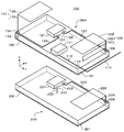
- It is a schematic diagram showing communication system 10A concerning a 2nd embodiment of the present invention.
- It is a schematic diagram showing the communication system 10B which concerns on the 3rd Embodiment of this invention.
- It is a schematic diagram showing 100 C of communication apparatuses which concern on the 4th Embodiment of this invention.
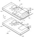
- FIG. 1 is a schematic view showing a communication system 10 according to a first embodiment of the present invention.
- the communication system 10 includes communication devices 100 and 200.
- the communication devices 100 and 200 communicate using a human body as a communication path.
- the communication device 100 can wirelessly communicate with an external device other than the communication device 200.
- the communication device 100 is incorporated in a portable wireless device and communicates with a base station.
- the communication device 100 includes a substrate 101, a ground portion 102, a communication portion 111, a signal line 112, a power feeding portion 113, an antenna 114, a communication portion 121, a terminal 122, a signal line 123, a terminal 124, a signal line 125, a conductor plate 126, a conductor A plate 127, terminals 131, and through holes 132 are provided.
- the substrate 101 is made of an insulating material (organic material (such as resin), composite material (such as a composite of glass fiber and resin)).
- the substrate 101 may be either a single layer or a multilayer. That is, it is also possible to constitute substrate 101 by a multilayer substrate which laminated a plurality of substrates. In this case, the conductor layer is disposed between the plurality of substrates.
- the ground portion 102 is disposed on the lower surface of the substrate 101, and is a conductor having a reference potential, for example, a metal layer.
- the communication unit 111 is disposed on the top surface of the substrate 101, and wirelessly communicates with an external device via an antenna 114 by radio waves.
- the signal line 112 is mounted on the substrate 101 and connects the power supply unit 113 and the communication unit 111.
- the feed unit 113 is disposed on the top surface of the substrate 101 and supplies power to the antenna 114.
- the antenna 114 is connected to the feeding unit 113, and transmits a wireless signal to an external device.
- the antenna 114 may operate as a receiving antenna for receiving a wireless signal from an external device.
- the antenna 114 may be a transmitting and receiving antenna capable of transmitting and receiving a wireless signal.
- the communication unit 121 is mounted on the substrate 101 and communicates with the communication device 200. That is, the communication unit 121 includes a transmission unit that transmits a signal to the communication device 200 and a reception unit that receives a signal from the communication device 200, and which one is to be connected to the terminal 122 can be switched.
- the terminals 122 and 131 are mounted on the communication unit 121, and are an input / output signal terminal of the communication unit 121 and a reference potential terminal.
- the terminal 122 is an input / output signal terminal mounted on the communication unit 121, and is connected to the signal line 123.
- the signal line 123 is mounted on the substrate, and both ends thereof are connected to the terminal 124 and the terminal 122.
- the terminals 124 are mounted on the substrate.
- the signal line 125 connects the terminal 124 and the conductor plate 126.
- the signal line 125 is a conductor line formed of a conductor element.
- the conductor plate 126 is connected to the end of the signal line 125.
- the conductor plate 127 is connected between the terminal 124 and the conductor plate 126 on the signal line 125.
- the whole of the conductor plates 126 and 127 constitutes an electrode 128.
- the terminal 131 is a reference potential terminal mounted on the communication unit 121, and is connected to the ground unit 102 through the through hole 132.
- the communication device 200 includes a substrate 201, a ground portion 202, a communication portion 221, terminals 222, signal lines 223, terminals 224, signal lines 225, conductor plates 226, terminals 231, and through holes 232.
- These substrates 201 and the like correspond to the substrate 101 of the communication device 100, the ground portion 102, the communication portion 121, the terminal 122, the signal line 123, the terminal 124, the signal line 125, the conductor plate 126, the terminal 131, and the through hole 132, respectively. , Omitted the detailed description.
- One or both of the conductor plates 126 and 127 of the communication device 100 capacitively couple with the surface of the human body.
- the conductor plate 226 of the communication device 200 is also electrostatically coupled to the surface of the same human body. That is, the conductor plates 126 and 127 of the communication device 100 and the conductor plate 226 of the communication device 200 are electrostatically coupled through the human body.
- ground portion 102 of the communication device 100 and the ground portion 202 of the communication device 200 are electrostatically coupled via a space.
- the signal (potential difference) generated by the communication unit 121 can be detected by the communication unit 221 of the communication device 200.
- the communication unit 121 can detect a signal (potential difference) generated by the communication unit 221 of the communication apparatus 200.
- the conductor plates 126 and 127 require a certain area to electrostatically couple with the surface of the human body.
- the current leaked from the feeding portion 113 to the substrate 101 flows from the terminal 124 through the signal line 125 to the conductor plates 127 and 126, thereby deteriorating the characteristics of the antenna 114.
- a method of adding a notch or a choke element to a substrate for example, JP 2008-300897 A, JP 2008-283464 A.
- a method of adding a 1 ⁇ 4 wavelength choke element to the outer conductor of the sleeve antenna In these methods, a choke element or the like is added at a position different from the radiation element portion of the antenna, and the choke element or the like does not contribute to radiation in the antenna.
- the length of the conductor plate 127 on the signal line 125 is approximately 1 ⁇ 4 of the wavelength of the operating frequency of the antenna 114, and the conductor plate 127 is operated as a choke stub. As a result, the current leaks from the feeding portion 113 onto the substrate 101 and flows through the terminal 124 and the signal line 125 to the conductor plate 126 is suppressed.
- the conductor plate 127 can also function as an electrode.
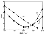
- FIG. 2 is a graph showing a frequency characteristic of a reflection characteristic VSWR (Voltag Standing Wave Ratio (voltage standing wave ratio)) when the antenna 114 is fed.
- FIG. 2 also shows the characteristics (graphs G2 and G3) of the communication devices 100X and 100Y according to comparative examples 1 and 2 in addition to the characteristic (graph G1) of the communication device 100 according to the present embodiment.
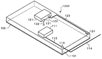
- 3 and 4 show the communication devices 100X and 100Y, respectively.
- the communication device 100 ⁇ / b> X according to the comparative example 1 does not have both the signal line 125 and the conductor plates 126 and 127.
- the communication device 100 ⁇ / b> Y according to the comparative example 2 does not have the conductor plate 127 (the conductor plate 126 is added).
- the VSWR characteristics of the antenna 114 in the comparative example 1 are 2 or less at the operating frequency (1975 MHz to 2050 MHz).
- Comparative Example 2 the communication device 100Y
- the conductor plate 126 is added, and the frequency characteristic of the antenna 114 is changed.
- the conductor plate 127 having a length of 1 ⁇ 4 of the wavelength of the operating frequency of the antenna 114 is connected.
- the frequency range in which the VSWR of the antenna 114 is 2 or less is substantially the same as in Comparative Example 1. That is, in the embodiment having the conductor plates 126 and 127, the comparative example 1 having no conductor plates 126 and 127 and the frequency range in which the antenna 114 operates, that is, the communication characteristics in the communication unit 111 are almost the same.
- the conductor plate 127 suppresses the leakage current flowing from the substrate 101 through the signal line 125 to the conductor plate 126.
- the conductor plate 127 plays a role as an electrode.
- the communication unit 121 communicates with the communication device 200
- the conductor plates 126 and 127 electrostatically couple with the electrodes 226 of the communication device 200.
- the conductor plates 126 and 127 are connected in parallel, the area of the electrode 128 is increased, and the coupling between the communication devices 100 and 200 is strengthened.
- the conductor plate 127 is installed on a surface different from the conductor plate 126. Since the surface of the electrode 128 electrostatically coupled to the electrode 226 of the communication device 200 is increased, the communication unit 121 can obtain diversity performance.
- the operating frequency range of the antenna 114 is 1975 MHz to 2050 MHz, but it is not limited to this frequency range.
- the operating frequency of the antenna 114 changes in accordance with the frequency used in the communication unit 111, and the conductor plate 127 also has a length of about 1 ⁇ 4 of the wavelength corresponding to the operating frequency of the first antenna 114.
- the communication device 100 can suppress the current leaked from the antenna 114 flowing to the electrode by the conductor plate 127, and the communication unit 111 can prevent the deterioration of the communication characteristics.
- the area of the electrode 128 can be expanded, and the diversity performance in the communication unit 121 can be obtained.
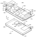
- FIG. 5 is a schematic view showing a communication system 10A according to a second embodiment of the present invention.
- the communication system 10A includes communication devices 100A and 200 that communicate with each other.
- a terminal 131, a signal line 133, a terminal 134, a signal line 135, and a conductor plate 136 are added to the communication device 100.
- An electrode 137 formed of the signal line 135 and the conductor plate 136 is connected to the terminal 134 mounted on the substrate 101.
- the terminal 134 is connected to the terminal 131 by the signal line 133 mounted on the substrate.
- the terminal 134 is also connected to the ground portion 102 by the through hole 132.
- the electrodes 128, 137 are each coupled to the electrodes 226, 202 of the communication device 200. Thereby, the potential difference between the two electrodes installed in one of the communication devices 100 and 200 can be transmitted between the two electrodes installed in the other communication device.
- the potential difference between the electrodes 128 and 137 is transmitted.
- the distance between the electrodes 128, 137 is small, coupling occurs at the electrodes 128, 137.
- the potential difference between the electrodes 128 and 137 is reduced, and the communication characteristics are degraded. Therefore, the electrodes 128 and 137 are disposed on the opposite longitudinal sides of the substrate 101 (the distance between the centers of the respective sides is maximum). The distance between the electrodes 128, 137 can be increased to suppress the reduction in coupling and potential difference between the electrodes 128, 137.
- the electrode 137 and the ground portion 102 are connected to constitute an electrode as a whole, and the electrode area can be enlarged.
- the electrode 128 is connected to a terminal 122 which is an input / output signal terminal, and the electrode 137 is connected to a terminal 131 which is a reference potential terminal.
- the connection terminals of the electrodes 128 and 137 may be interchanged.
- the electrode 128 is connected to the terminal 131 which is a reference potential terminal, the terminal 134 is not connected to the ground portion 102, and the terminal 124 is connected to the ground portion 102 by a through hole. As a result, the effective area of the electrode 128 is enlarged.
- FIG. 6 is a schematic view showing a communication system 10B according to a third embodiment of the present invention.
- the communication system 10B includes communication devices 100B and 200 that communicate with each other.
- a communication unit 141, a signal line 142, a power feeding unit 143, an antenna 144, and a conductor plate 138 are added to the communication device 100.
- a feeding portion 143 is provided on an end side of the substrate 101 on which the terminal 134 to which the conductor plate 136 is connected is mounted, and the antenna 144 is connected to the feeding portion 143.
- the power supply unit 143 is connected to the communication unit 141 mounted on the substrate 101 by the signal line 142.
- a conductor plate 138 having a length of 1 ⁇ 4 of the wavelength of the operating frequency of the antenna 144 is connected to the signal line 135.
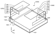
- FIG. 7 is a schematic view showing a communication device 100C of the communication system 10C according to the fourth embodiment of the present invention.
- the communication system 10C includes communication devices 100C and 200 that communicate with each other. Note that only a part of the communication device 100C is shown, and the communication device 200 is not shown.
- a conductor plate 161, switches 162 and 163, a conductor plate 151, and switches 152 and 153 are added to the communication device 100.
- the electrode 128C is configured by the signal line 125, the conductor plates 126, 127, 161, and the switches 162, 163.
- An electrode 137C is constituted by the signal line 135, the conductor plates 136, 138, 151, and the switches 152, 153.
- Conductor plates 126 and 161 are connected to signal line 125 by switches 162 and 163, respectively.
- the electrode 137C has the conductor plates 136 and 151 connected to the signal line 135 by switches 152 and 153, respectively.
- the conductor plates 126 and 161 can be fixed to, for example, the housing of the communication terminal device.
- the switches 162, 163, 152, 153 can be controlled by the communication unit 121.
- the communication unit 121 to which the electrodes 128C and 137C are connected measures the potential difference between the electrodes 128C and 137C when the signal from the communication device 200 is received. Based on the result, the connection state between the switches 162, 163, 152, 153 and the conductor plates 126, 161, 136, 138 is controlled so that the potential difference between the electrodes 128C, 137C is maximized. By doing this, it is possible to maximize transmission power and reception power.
- the number of conductive plates connected by the switch is two for both the electrodes 128C and 137C, but the number may be changed according to the configuration.
- FIG. 8 is a schematic view showing a communication device 100D of a communication system 10D according to a fifth embodiment of the present invention.
- the communication system 10D includes communication devices 100D and 200 that communicate with each other. Only a part of the communication device 100D is shown, and the communication device 200 is not shown.
- a conductor plate 171 and a switch 172 are added to the communication device 100.
- the electrode 128 C is composed of a signal line 125, three conductor plates 126, 127, 171, and a switch 172. One of the conductor plates 127 and 171 is connected to the signal line 125 by the switch 172.
- the switch 172 is connected to the communication unit 111 via a control line (not shown) and controlled.
- the antenna 114 is an antenna having a wide band or a characteristic having a plurality of resonant frequencies, and the communication unit 111 may switch between a plurality of frequencies for communication. In this case, it is preferable to change the length of the conductor plate 127 each time the frequency is switched. Here, it is difficult to change the length of the conductor plate 127 once installed. Then, the conductor boards 127 and 171 according to the frequency used by the communication part 111 are installed beforehand. When the communication unit 111 communicates, a control signal corresponding to the frequency to be used is transmitted to the switch 172 through the control line. As a result, the switch 172 connects the conductor plates 127 and 171 corresponding to the control signal to the signal line 125. By doing this, even if the electrode 128 is an antenna with a characteristic that the antenna 114 has a wide band or a plurality of resonance frequencies, it is possible to prevent the deterioration of the antenna performance at the frequency used by the communication unit 111.
- a conductor plate which is not selected and is not connected to the signal line 125 may be connected to the conductor plate 126 by a switch.
- the conductor plate not selected is connected to the conductor plate 126, the effect of enlarging the electrode area is obtained.
- the conductor plates 127 and 171 are disposed in the same plane. On the other hand, as long as the conductor plate 126 on the signal line 125 and the substrate 101 are connected, the conductor plates 127 and 171 may not be installed in the same plane.
- the conductor plate 171 and the switch 172 may be added to the communication device 100B according to the third embodiment.
- the antenna 144 is also an antenna having a wide band or a characteristic having a plurality of resonance frequencies, and the communication unit 141 performs communication by switching a plurality of frequencies.
- the electrode 137B may have the same configuration as the electrode 128D of the present embodiment, and the conductor plate 138 and another electrode may be switched and used.
- FIG. 9 is a schematic view showing a communication device 100E of a communication system 10E according to a sixth embodiment of the present invention.
- the communication system 10E includes communication devices 100E and 200 that communicate with each other. Note that only a part of the communication device 100E is shown, and the communication device 200 is not shown.
- switches 181 and 182 are added to the communication apparatus 100.
- the electrode 128E is configured by the signal line 125, the conductor plates 126 and 127, and the switches 181 and 182.
- the conductor plate 127 is connected to the conductor plate 126 and the terminal 183 on the substrate 101 by the switches 181 and 182.
- the terminal 183 on the substrate 101 is connected to the ground portion 102 by the through hole 184.
- the switches 181 and 182 are connected to the communication unit 111 via a control line (not shown) and controlled.
- the electrical length of the conductor plate 127 can be changed by switching the connection state of the conductor plate 127 to the conductor plate 126 and the ground portion 102 by the switches 181 and 182 as described above. For this reason, even if the antenna 114 is an antenna having a wide band or a characteristic having a plurality of resonance frequencies, it is possible to prevent deterioration of the antenna performance at the frequency used by the communication unit 111.
- switches 181 and 182 may be added to the communication apparatus 100B according to the third embodiment.
- the antenna 144 is also an antenna having a wide band or a characteristic having a plurality of resonance frequencies, and the communication unit 141 performs communication by switching a plurality of frequencies.
- the electrode 137B may have the same configuration as the electrode 128E of the present embodiment, and the conductor plate 138 and another electrode may be switched and used.
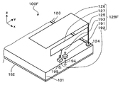
- FIG. 10 is a schematic view showing a communication device 100F of a communication system 10F according to a seventh embodiment of the present invention.
- the communication system 10F includes communication devices 100F and 200 that communicate with each other. Note that only a part of the communication device 100F is shown, and the communication device 200 is not shown.
- capacitors 191 and 192 and a switch 193 are added to the communication device 100.
- Capacitors 191 and 192 are disposed on the substrate 101 under the conductor plate 127. Capacitors 191 and 192 are connected to conductor plate 127 by switch 193. Capacitors 191 and 192 are connected to ground portion 102 by through holes 194 and 195. The switch 193 is connected to the communication unit 111 via a control line (not shown) and controlled.
- a control signal corresponding to the frequency to be used is transmitted to the switch 193 through the control line.
- the switch 193 is connected to either or neither of the capacitors 191 and 192.
- the conductor plate 127 can be changed to an electrical length corresponding to the frequency used by the communication unit 111. That is, even if the antenna 114 is an antenna having a wide band or a characteristic having a plurality of resonance frequencies, deterioration of the antenna performance can be prevented.
- the number of capacitors may be changed according to the frequency used by the communication unit 111 to be three or more.
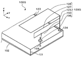
- variable capacitance element 195 is connected to the communication unit 111 by a control line.
- a control signal corresponding to the frequency used by the communication unit 111 is transmitted from the communication unit 111 via the control line to the switch 193 and the variable capacitance. It is sent to each of the elements 195.
- the switch 193 is in a state in which the conductor plate 127 and the variable capacitance element 195 are connected, and the variable capacitance element 195 has a capacitance value according to the control signal.
- the conductor plate 127 has an electrical length corresponding to the frequency used by the communication unit 111. That is, even if the antenna 114 is an antenna having a wide band or a characteristic having a plurality of resonance frequencies, it is possible to prevent deterioration of antenna performance at a frequency used by the communication unit 111.
- capacitors 191 and 192 and a switch 193 may be added to the communication device 100B according to the third embodiment.
- the antenna 144 is also an antenna having a wide band or a characteristic having a plurality of resonance frequencies, and the communication unit 141 performs communication by switching a plurality of frequencies.
- the electrode 137B may have the same configuration as the electrode 128F of this embodiment, and the presence or absence of connection of a capacitor may be switched.
Landscapes
- Engineering & Computer Science (AREA)
- Computer Networks & Wireless Communication (AREA)
- Signal Processing (AREA)
- Transceivers (AREA)
- Support Of Aerials (AREA)
Abstract
通信装置が、基板と、前記基板に配置されるアンテナと、前記アンテナを介して所定の周波数で信号を送信又は受信する第1の通信部と、第1の導体板と、前記基板に配置され、前記第1の導体板と導体線で接続される端子と、前記基板に配置され、前記端子と電気的に接続され、前記第1の導体板を介して通信相手と通信を行う第2の通信部と、前記導体線と電気的に接続され、前記所定の周波数の略1/4波長の長さを有する第2導体板と、を具備する。
Description
本発明は、通信装置に関する。
人体を伝送路とし、機器間で通信する通信システムがある(例えば、特許文献1参照)。この通信システムでは、機器内に一対の電極が設置される。一つは信号を送受信するための信号電極であり、もう一方は基準電位を伝達するための基準電極である。機器は互いの信号電極と基準電極どうしが静電結合し、電極間の電位差を伝達することで、通信する。
上記通信システムでは、機器間での結合を安定化させるため電極の面積が大きい方が好ましい。また、機器内部で信号電極と基準電極がショートしてしまうと電位差が小さくなるので、機器内部では一対の電極を離しておく必要がある。そのため、携帯電話などの小形無線端末を上記通信システムの機器としても動作可能にする場合、一対の電極を小形無線端末の両端に設置することが好ましい。
しかし、小形無線端末の端部にアンテナが設置されることが多く、アンテナと電極が同一端部に設置される可能性が高い。この結果、電極がアンテナ性能を劣化させる可能性がある。
本発明は、電極によるアンテナ性能の劣化を低減した通信装置を提供することを目的とする。
しかし、小形無線端末の端部にアンテナが設置されることが多く、アンテナと電極が同一端部に設置される可能性が高い。この結果、電極がアンテナ性能を劣化させる可能性がある。
本発明は、電極によるアンテナ性能の劣化を低減した通信装置を提供することを目的とする。
本発明の一態様に係る通信装置は、基板と、前記基板に配置されるアンテナと、前記アンテナを介して所定の周波数で信号を送信又は受信する第1の通信部と、第1の導体板と、前記基板に配置され、前記第1の導体板と導体線で接続される端子と、前記基板に配置され、前記端子と電気的に接続され、前記第1の導体板を介して通信相手と通信を行う第2の通信部と、前記導体線と電気的に接続され、前記所定の周波数の略1/4波長の長さを有する第2導体板と、を具備する。
本発明によれば、電極によるアンテナ性能の劣化を低減した通信装置を提供できる。
以下、図面を参照しながら本実施の形態について詳細に説明する。
(第1の実施形態)
図1は本発明の第1の実施形態に係る通信システム10を表す模式図である。通信システム10は、通信装置100、200を有する。通信装置100、200は人体を通信経路として通信する。また、通信装置100は、通信装置200以外の外部機器と無線通信が可能であり、例えば、携帯無線機に内蔵され、基地局と通信する。
図1は本発明の第1の実施形態に係る通信システム10を表す模式図である。通信システム10は、通信装置100、200を有する。通信装置100、200は人体を通信経路として通信する。また、通信装置100は、通信装置200以外の外部機器と無線通信が可能であり、例えば、携帯無線機に内蔵され、基地局と通信する。
通信装置100は、基板101、グランド部102、通信部111、信号線112、給電部113、アンテナ114、通信部121、端子122、信号線123、端子124、信号線125、導体板126、導体板127、端子131、スルーホール132を有する。
基板101は、絶縁材料(有機材料(樹脂等)、複合材料(ガラス繊維と樹脂の複合体等))から構成される。なお、基板101は、単層、多層の何れであっても良い。即ち、基板101を複数の基板を積層した多層基板で構成することも可能である。この場合、複数の基板間に導体層が配置される。
グランド部102は、基板101の下面に配置され、基準電位を有する導体、例えば、金属層である。
通信部111は、基板101の上面に配置され、アンテナ114を介して、外部機器と電波により無線通信する。
信号線112は、基板101上に実装され、給電部113と通信部111を接続する。
給電部113は、基板101の上面に配置され、アンテナ114に電力を供給する。
アンテナ114は、給電部113に接続され、外部機器に無線信号を送信する。あるいは、アンテナ114が外部機器から無線信号を受信する受信アンテナとして動作してもよい。また、アンテナ114が、無線信号を送信及び受信可能な送受信アンテナであってもよい。
信号線112は、基板101上に実装され、給電部113と通信部111を接続する。
給電部113は、基板101の上面に配置され、アンテナ114に電力を供給する。
アンテナ114は、給電部113に接続され、外部機器に無線信号を送信する。あるいは、アンテナ114が外部機器から無線信号を受信する受信アンテナとして動作してもよい。また、アンテナ114が、無線信号を送信及び受信可能な送受信アンテナであってもよい。
通信部121は、基板101上に実装され、通信装置200と通信する。即ち、通信部121は、通信装置200に信号を送信する送信部と、通信装置200からの信号を受信する受信部とを有し、このいずれを端子122に接続するかを切り替えられる。
端子122、131はそれぞれ、通信部121に実装され、通信部121の入出力信号端子、基準電位端子である。
端子122は、通信部121に実装される入出力信号端子であり、信号線123に接続される。
信号線123は、基板上に実装され、両端が端子124と端子122に接続される。
端子124は、基板上に実装される。
信号線123は、基板上に実装され、両端が端子124と端子122に接続される。
端子124は、基板上に実装される。
信号線125は、端子124と導体板126とを接続する。信号線125は、導体素子で構成される導体線である。
導体板126は、信号線125の端部に接続される。
導体板127は、信号線125上で端子124と導体板126の間に接続される。
導体板126、127の全体が電極128を構成する。
導体板126は、信号線125の端部に接続される。
導体板127は、信号線125上で端子124と導体板126の間に接続される。
導体板126、127の全体が電極128を構成する。
端子131は、通信部121に実装される基準電位端子であり、スルーホール132を介して、グランド部102に接続される。
通信装置200は、基板201、グランド部202、通信部221、端子222、信号線223、端子224、信号線225、導体板226、端子231、スルーホール232を有する。これら基板201等は、通信装置100の基板101、グランド部102、通信部121、端子122、信号線123、端子124、信号線125、導体板126、端子131、スルーホール132とそれぞれ対応するため、詳細な説明を省略する。
(通信システム10の動作)
通信装置100の導体板126、127の一方または双方が人体の表面と静電結合する。通信装置200の導体板226も同一人体の表面と静電結合する。即ち、通信装置100の導体板126、127と通信装置200の導体板226が人体を介して静電結合する。
通信装置100の導体板126、127の一方または双方が人体の表面と静電結合する。通信装置200の導体板226も同一人体の表面と静電結合する。即ち、通信装置100の導体板126、127と通信装置200の導体板226が人体を介して静電結合する。
一方、通信装置100のグランド部102と通信装置200のグランド部202が空間を介して静電結合する。
この結果、通信部121が発した信号(電位差)を通信装置200の通信部221で検知できる。逆に、通信装置200の通信部221が発した信号(電位差)を通信部121で検知できる。
導体板126や127は、人体表面と静電結合するために、ある程度の面積が必要である。基板101上に導体板126や127が接続されると、給電部113から基板101に漏洩した電流が、端子124から信号線125をとおり導体板127や126に流れ、アンテナ114の特性を劣化させてしまう。
給電部113から漏洩して基板101上に流れる電流を抑制することで、アンテナの特性を改善する手法が存在する。例えば、基板に切り込みやチョーク素子を付加する手法がある(例えば、特開2008-300897公報、特開2008-283464公報)。また、スリーブアンテナの外導体に1/4波長のチョーク素子を付加する手法がある。これらの手法では、アンテナの放射素子部分と異なる位置にチョーク素子等が付加され、チョーク素子等はアンテナでの放射には寄与しない。
ここでは、信号線125上の導体板127の長さをアンテナ114の動作周波数の波長の略1/4とし、導体板127をチョークスタブとして動作させる。これにより、給電部113から基板101上に漏洩し、端子124、信号線125を経由して導体板126に流れる電流が抑圧される。また、導体板127は、電極としても機能できる。
図2は、アンテナ114を給電したときの反射特性VSWR(Voltag Standing Wave Ratio(電圧定在波比))の周波数特性を示すグラフである。図2には、本実施形態に係る通信装置100の特性(グラフG1)に加え、比較例1、2に係る通信装置100X、100Yの特性(グラフG2、G3)も表している。図3、図4がそれぞれ通信装置100X、100Yを表す。
図3に示すように、比較例1に係る通信装置100Xは、信号線125および導体板126、127の双方を有しない。図4に示すように、比較例2に係る通信装置100Yは、導体板127を有しない(導体板126が付加されている)。
比較例1(通信装置100X)でのアンテナ114のVSWR特性は動作周波数(1975MHz~2050MHz)で2以下である。比較例2(通信装置100Y)では、導体板126が付加され、アンテナ114の周波数特性が変化している。このように周波数特性がずれることによって、通信部111と外部機器との通信特性が劣化する。実施例(通信装置100)では、アンテナ114の動作周波数の波長の1/4の長さの導体板127が接続されている。この結果、アンテナ114のVSWRが2以下となる周波数範囲は比較例1とほぼ同様となる。即ち、導体板126、127を有する実施例は、導体板126、127を有しない比較例1と、アンテナ114の動作する周波数範囲、即ち、通信部111での通信特性がほぼ同一である。
このように、導体板127は、基板101から信号線125を通って導体板126に流れる漏洩電流を抑圧する。これに加え、導体板127は、電極としての役割を果たす。通信部121が通信装置200と通信するとき、導体板126、127は通信装置200の電極226と静電的に結合する。このとき、導体板126と127は並列に接続されているので、電極128の面積が増大し、通信装置100、200間の結合が強くなる。
図1では、導体板127が導体板126と異なる面に設置される。通信装置200の電極226と静電結合する電極128の面が増えるので、通信部121はダイバーシチ性能を得ることができる。
なお、本実施例ではアンテナ114の動作周波数範囲を1975MHz~2050MHzとしたが、この周波数範囲に限るものではない。通信部111で使用される周波数に応じてアンテナ114の動作周波数は変わり、導体板127もアンテナ第1の114の動作周波数に応じた波長の略1/4の長さとなる。
このように通信装置100は、導体板127によって、電極に流れるアンテナ114から漏洩する電流を抑圧し、通信部111で通信特性の劣化を防ぐことができる。これに加えて、電極128の面積を拡大し、かつ通信部121でのダイバーシチ性能を得ることができる。
(第2の実施形態)
図5は本発明の第2の実施形態に係る通信システム10Aを表す模式図である。通信システム10Aは、互いに通信する通信装置100A、200を有する。
図5は本発明の第2の実施形態に係る通信システム10Aを表す模式図である。通信システム10Aは、互いに通信する通信装置100A、200を有する。
通信装置100Aは、通信装置100に、端子131、信号線133、端子134、信号線135、導体板136が付加されている。
基板101上に実装された端子134に信号線135と導体板136とで構成された電極137が接続されている。そして、端子134は、基板上に実装された信号線133によって端子131と接続される。端子134は、スルーホール132によってグランド部102にも接続される。
電極128、137は、それぞれが通信装置200の電極226、202に結合している。これにより、通信装置100、200の一方に設置された2つの電極間の電位差を、他方の通信装置に設置された2つの電極間に伝達できる。
上述したように、通信部121での通信では電極128、137間の電位差を伝達する。電極128、137の距離が狭いと、電極128、137で結合が生じる。この結果、電極128、137間の電位差が小さくなり、通信特性が劣化する。そこで、電極128、137を基板101の対向する長手側の辺に配置する(それぞれの辺の中心間の距離が最大)。電極128、137の距離を広くして、電極128、137間の結合および電位差の減少を抑制できる。
また、電極137とグランド部102が接続され、全体として電極が構成され、電極面積を拡大できる。
本実施形態では、電極128が入出力信号端子である端子122に接続され、電極137が基準電位端子である端子131に接続されている。一方、電極128、137の接続端子が入れ替わっても構わない。電極128が基準電位端子である端子131に接続されている場合は、端子134はグランド部102と接続されず、端子124がスルーホールでグランド部102に接続される。その結果、電極128の実効的な面積が拡大される。
(第3の実施形態)
図6は本発明の第3の実施形態に係る通信システム10Bを表す模式図である。通信システム10Bは、互いに通信する通信装置100B、200を有する。
図6は本発明の第3の実施形態に係る通信システム10Bを表す模式図である。通信システム10Bは、互いに通信する通信装置100B、200を有する。
通信装置100Bは、通信装置100に、通信部141、信号線142、給電部143、アンテナ144、導体板138が付加されている。導体板136が接続される端子134が実装されている基板101の端辺部に給電部143が設けられ、給電部143にアンテナ144が接続される。給電部143は基板101に実装された通信部141と、信号線142で接続されている。そして、信号線135上にはアンテナ144の動作周波数の波長の1/4の長さの導体板138が接続されている。
このように導体板138を信号線135に接続することで、電極が接続されている同じ端辺部に接続されているアンテナ144の性能の劣化を防げる。
(第4の実施形態)
図7は本発明の第4の実施形態に係る通信システム10Cの通信装置100Cを表す模式図である。通信システム10Cは、互いに通信する通信装置100C、200を有する。なお、通信装置100Cの一部のみを示し、通信装置200は図示を省略している。
図7は本発明の第4の実施形態に係る通信システム10Cの通信装置100Cを表す模式図である。通信システム10Cは、互いに通信する通信装置100C、200を有する。なお、通信装置100Cの一部のみを示し、通信装置200は図示を省略している。
通信装置100Cは、通信装置100に、導体板161、スイッチ162、163、導体板151、スイッチ152、153が付加されている。電極128Cが、信号線125、導体板126、127、161、スイッチ162、163によって構成される。電極137Cが、信号線135、導体板136、138、151、スイッチ152、153によって構成される。
導体板126と161がそれぞれスイッチ162と163によって信号線125に接続されている。電極137Cは導体板136と151がそれぞれスイッチを152と153によって信号線135に接続されている。導体板126および161は例えば通信端末機器の筐体に固定された状態とすることができる。スイッチ162、163、152、153は、通信部121により、制御可能とする。
電極128C、137Cが接続されている通信部121では、通信装置200からの信号の受信時に、電極128C、137C間の電位差を測定する。その結果に基づいて、電極128C、137C間の電位差が最大となるようにスイッチ162、163、152、153と導体板126、161、136、138との接続状態を制御する。このようにすることで、送信電力および受信電力を最大にすることが可能である。
なお、本実施形態では、スイッチによって接続される導体板は電極128C、137Cともに2つであったが、構成に応じて個数を変化させてもよい。
なお、本実施形態では、スイッチによって接続される導体板は電極128C、137Cともに2つであったが、構成に応じて個数を変化させてもよい。
(第5の実施形態)
図8は本発明の第5の実施形態に係る通信システム10Dの通信装置100Dを表す模式図である。通信システム10Dは、互いに通信する通信装置100D、200を有する。なお、通信装置100Dの一部のみを示し、通信装置200は図示を省略している。
図8は本発明の第5の実施形態に係る通信システム10Dの通信装置100Dを表す模式図である。通信システム10Dは、互いに通信する通信装置100D、200を有する。なお、通信装置100Dの一部のみを示し、通信装置200は図示を省略している。
通信装置100Dは、通信装置100に、導体板171、スイッチ172が付加されている。
電極128Cが、信号線125、3つの導体板126、127、171、スイッチ172で構成されている。導体板127と171はスイッチ172によって、どちらか一方が信号線125に接続される。スイッチ172は、通信部111と図示しない制御線で接続され、制御されるものとする。
アンテナ114が広帯域もしくは共振周波数を複数有する特性のアンテナであり、通信部111が複数の周波数を切り替えて通信することがある。この場合、周波数が切り替わるごとに導体板127の長さを変化することが好ましい。ここで、一度設置された導体板127の長さを変えることは難しい。そこで、あらかじめ通信部111で使用する周波数に応じた導体板127、171を設置する。通信部111が通信するとき、使用する周波数に応じた制御信号が制御線を通してスイッチ172へ送信される。この結果、スイッチ172が制御信号に対応した導体板127、171と信号線125を接続する。このようにすることで、電極128は、アンテナ114が広帯域もしくは共振周波数を複数有する特性のアンテナであっても、通信部111が使用する周波数でのアンテナ性能の劣化を防ぐことができる。
図示はしていないが、選択されずに信号線125に接続していない状態となった導体板が導体板126にスイッチによって接続されていてもよい。選択されなかった導体板が導体板126に接続されると、電極面積を拡大した効果が得られる。
本実施形態では導体板127と171は同一面内に設置されている。これに対して、信号線125上の導体板126と基板101の間で接続されていれば、導体板127と171が同一面内に設置されていなくてもよい。
また、第3の実施形態に係る通信装置100Bに、導体板171、スイッチ172を付加しても良い。ここで、アンテナ144が同様に広帯域もしくは共振周波数を複数有する特性のアンテナであり、通信部141が複数の周波数を切り替えて通信することが考えられる。この場合、電極137Bにも、本実施形態の電極128Dと同様の構成とし、導体板138と他の電極を切り替えて用いるようにしても良い。
(第6の実施形態)
図9は本発明の第6の実施形態に係る通信システム10Eの通信装置100Eを表す模式図である。通信システム10Eは、互いに通信する通信装置100E、200を有する。なお、通信装置100Eの一部のみを示し、通信装置200は図示を省略している。
図9は本発明の第6の実施形態に係る通信システム10Eの通信装置100Eを表す模式図である。通信システム10Eは、互いに通信する通信装置100E、200を有する。なお、通信装置100Eの一部のみを示し、通信装置200は図示を省略している。
通信装置100Eは、通信装置100に、スイッチ181、182が付加されている。
電極128Eが、信号線125、導体板126、127、スイッチ181、182で構成されている。導体板127がスイッチ181と182によって、導体板126と基板101上の端子183に接続されている。基板101上の端子183はスルーホール184によりグランド部102に接続されている。スイッチ181、182は、通信部111と図示しない制御線で接続され、制御されるものとする。
このようにスイッチ181、182によって導体板127を導体板126とグランド部102への接続状態を切り替えることで、導体板127の電気長を変えることができる。このため、アンテナ114が広帯域もしくは共振周波数を複数有する特性のアンテナであっても、通信部111が使用する周波数でのアンテナ性能の劣化を防ぐことができる。
また、第3の実施形態に係る通信装置100Bに、スイッチ181、182を付加しても良い。ここで、アンテナ144が同様に広帯域もしくは共振周波数を複数有する特性のアンテナであり、通信部141が複数の周波数を切り替えて通信することが考えられる。この場合、電極137Bにも、本実施形態の電極128Eと同様の構成とし、導体板138と他の電極を切り替えて用いるようにしても良い。
(第7の実施形態)
図10は本発明の第7の実施形態に係る通信システム10Fの通信装置100Fを表す模式図である。通信システム10Fは、互いに通信する通信装置100F、200を有する。なお、通信装置100Fの一部のみを示し、通信装置200は図示を省略している。
図10は本発明の第7の実施形態に係る通信システム10Fの通信装置100Fを表す模式図である。通信システム10Fは、互いに通信する通信装置100F、200を有する。なお、通信装置100Fの一部のみを示し、通信装置200は図示を省略している。
通信装置100Fは、通信装置100に、コンデンサ191、192、スイッチ193が付加されている。
導体板127の下の基板101上にコンデンサ191と192が配置される。コンデンサ191と192はスイッチ193によって導体板127と接続される。コンデンサ191と192は、スルーホール194、195によってグランド部102に接続されている。スイッチ193は、通信部111と図示しない制御線で接続され、制御されるものとする。
通信部111が通信するとき、使用する周波数に応じた制御信号が制御線を通してスイッチ193へ送信される。その結果、制御信号に応じて、スイッチ193がコンデンサ191と192のどちらかに接続またはどちらとも接続しない状態になる。このようにすることで、導体板127は通信部111が使用する周波数に応じた電気長に変えることができる。即ち、アンテナ114が広帯域もしくは共振周波数を複数有する特性のアンテナであっても、アンテナ性能の劣化を防ぐことができる。
コンデンサの数は通信部111が使用する周波数に応じて、変化させ、3個以上としても良い。
また、図11のように可変容量素子195を用いることも可能である。可変容量素子195は通信部111と制御線で接続されている。通信部111が使用する周波数に応じて、導体板127の電気長を変えるとき、通信部111からは、通信部111が使用する周波数に応じた制御信号が制御線を介してスイッチ193と可変容量素子195のそれぞれに送られる。そして、スイッチ193は導体板127と可変容量素子195を接続した状態になり、可変容量素子195は制御信号に応じた容量値となる。
これによって、導体板127は通信部111が使用する周波数に応じた電気長となる。即ち、アンテナ114が広帯域もしくは共振周波数を複数有する特性のアンテナであっても、通信部111が使用する周波数でのアンテナ性能の劣化を防ぐことができる。
これによって、導体板127は通信部111が使用する周波数に応じた電気長となる。即ち、アンテナ114が広帯域もしくは共振周波数を複数有する特性のアンテナであっても、通信部111が使用する周波数でのアンテナ性能の劣化を防ぐことができる。
また、第3の実施形態に係る通信装置100Bに、コンデンサ191、192、スイッチ193を付加しても良い。ここで、アンテナ144が同様に広帯域もしくは共振周波数を複数有する特性のアンテナであり、通信部141が複数の周波数を切り替えて通信することが考えられる。この場合、電極137Bにも、本実施形態の電極128Fと同様の構成とし、コンデンサの接続の有無等を切り替えても良い。
(その他の実施形態)
本発明の実施形態は上記の実施形態に限られず拡張、変更可能であり、拡張、変更した実施形態も本発明の技術的範囲に含まれる。
本発明の実施形態は上記の実施形態に限られず拡張、変更可能であり、拡張、変更した実施形態も本発明の技術的範囲に含まれる。
10…通信システム、100、200…通信装置、101…基板、101…基板、102…グランド部、111…通信部、112…信号線、113…給電部、114…アンテナ、121…通信部、122…端子、123…信号線、124…端子、125…信号線、126、127…導体板、128…電極
Claims (5)
- 基板と、
前記基板に配置されるアンテナと、
前記アンテナを介して所定の周波数で信号を送信又は受信する第1の通信部と、
第1の導体板と、
前記基板に配置され、前記第1の導体板と導体線で接続される端子と、
前記基板に配置され、前記端子と電気的に接続され、前記第1の導体板を介して通信相手と通信を行う第2の通信部と、
前記導体線と電気的に接続され、前記所定の周波数の略1/4波長の長さを有する第2導体板と、
を具備することを特徴とする通信装置。 - 前記第1、第2の導体板が略直交する
ことを特徴とする請求項1記載の通信装置。 - 前記基板に配置され、前記第2の通信部と電気的に接続される第3の導体板、をさらに具備し、
前記第2の通信部が、信号端子と基準電位端子を有し、
前記端子が前記信号端子に接続され、前記第3の導体板が前記基準電位端子に接続される、
ことを特徴とする請求項2記載の通信装置。 - 前記基板が長方形であり、
前記第1、第2の端子が、前記基板の長手方向に配置される、
ことを特徴とする請求項3記載の通信装置。 - 前記第1、第2の導体板の電気的接続の有無を切り替える第1のスイッチと、
前記基板と前記第2の導体板の電気的接続の有無を切り替える第2のスイッチと、
をさらに具備することを特徴とする請求項4記載の通信装置。
Priority Applications (3)
| Application Number | Priority Date | Filing Date | Title |
|---|---|---|---|
| JP2011531664A JP5330523B2 (ja) | 2009-09-18 | 2009-09-18 | 通信装置 |
| PCT/JP2009/004773 WO2011033593A1 (ja) | 2009-09-18 | 2009-09-18 | 通信装置 |
| US13/361,011 US8847827B2 (en) | 2009-09-18 | 2012-01-30 | Communication apparatus |
Applications Claiming Priority (1)
| Application Number | Priority Date | Filing Date | Title |
|---|---|---|---|
| PCT/JP2009/004773 WO2011033593A1 (ja) | 2009-09-18 | 2009-09-18 | 通信装置 |
Related Child Applications (1)
| Application Number | Title | Priority Date | Filing Date |
|---|---|---|---|
| US13/361,011 Continuation US8847827B2 (en) | 2009-09-18 | 2012-01-30 | Communication apparatus |
Publications (1)
| Publication Number | Publication Date |
|---|---|
| WO2011033593A1 true WO2011033593A1 (ja) | 2011-03-24 |
Family
ID=43758221
Family Applications (1)
| Application Number | Title | Priority Date | Filing Date |
|---|---|---|---|
| PCT/JP2009/004773 Ceased WO2011033593A1 (ja) | 2009-09-18 | 2009-09-18 | 通信装置 |
Country Status (3)
| Country | Link |
|---|---|
| US (1) | US8847827B2 (ja) |
| JP (1) | JP5330523B2 (ja) |
| WO (1) | WO2011033593A1 (ja) |
Cited By (2)
| Publication number | Priority date | Publication date | Assignee | Title |
|---|---|---|---|---|
| JP2013121034A (ja) * | 2011-12-07 | 2013-06-17 | Toshiba Corp | 通信装置 |
| JP2013223160A (ja) * | 2012-04-18 | 2013-10-28 | Toshiba Corp | 通信装置 |
Citations (4)
| Publication number | Priority date | Publication date | Assignee | Title |
|---|---|---|---|---|
| JPH07202774A (ja) * | 1993-12-28 | 1995-08-04 | Toshiba Corp | 無線装置 |
| JP2005004383A (ja) * | 2003-06-10 | 2005-01-06 | Nippon Telegr & Teleph Corp <Ntt> | 電界利用監視システム |
| JP2008205604A (ja) * | 2007-02-16 | 2008-09-04 | Mitsubishi Denki Tokki System Kk | アンテナ装置 |
| JP2009065666A (ja) * | 2000-10-24 | 2009-03-26 | Sony Corp | 情報処理装置、電子機器、通信システム |
Family Cites Families (9)
| Publication number | Priority date | Publication date | Assignee | Title |
|---|---|---|---|---|
| JP3595930B2 (ja) | 1998-11-16 | 2004-12-02 | 三和シヤッター工業株式会社 | 建築用電動開閉装置 |
| JP4868195B2 (ja) | 2000-10-24 | 2012-02-01 | ソニー株式会社 | 電子機器および情報処理装置 |
| JP4019742B2 (ja) | 2001-05-14 | 2007-12-12 | ソニー株式会社 | 情報伝送装置及び情報伝送システム |
| JP2007194842A (ja) * | 2006-01-18 | 2007-08-02 | Fujitsu Component Ltd | 通信装置 |
| JP4804447B2 (ja) * | 2006-12-05 | 2011-11-02 | パナソニック株式会社 | アンテナ装置及び無線通信装置 |
| JP4962723B2 (ja) * | 2007-02-20 | 2012-06-27 | ミツミ電機株式会社 | アンテナ素子および広帯域アンテナ装置 |
| JP4738380B2 (ja) | 2007-05-10 | 2011-08-03 | 株式会社東芝 | 電子機器 |
| JP2008300897A (ja) | 2007-05-29 | 2008-12-11 | Ngk Spark Plug Co Ltd | アンテナ装置 |
| WO2009044540A1 (ja) * | 2007-10-02 | 2009-04-09 | Panasonic Corporation | 携帯無線通信装置 |
-
2009
- 2009-09-18 WO PCT/JP2009/004773 patent/WO2011033593A1/ja not_active Ceased
- 2009-09-18 JP JP2011531664A patent/JP5330523B2/ja not_active Expired - Fee Related
-
2012
- 2012-01-30 US US13/361,011 patent/US8847827B2/en active Active
Patent Citations (4)
| Publication number | Priority date | Publication date | Assignee | Title |
|---|---|---|---|---|
| JPH07202774A (ja) * | 1993-12-28 | 1995-08-04 | Toshiba Corp | 無線装置 |
| JP2009065666A (ja) * | 2000-10-24 | 2009-03-26 | Sony Corp | 情報処理装置、電子機器、通信システム |
| JP2005004383A (ja) * | 2003-06-10 | 2005-01-06 | Nippon Telegr & Teleph Corp <Ntt> | 電界利用監視システム |
| JP2008205604A (ja) * | 2007-02-16 | 2008-09-04 | Mitsubishi Denki Tokki System Kk | アンテナ装置 |
Cited By (4)
| Publication number | Priority date | Publication date | Assignee | Title |
|---|---|---|---|---|
| JP2013121034A (ja) * | 2011-12-07 | 2013-06-17 | Toshiba Corp | 通信装置 |
| US9014630B2 (en) | 2011-12-07 | 2015-04-21 | Kabushiki Kaisha Toshiba | Communication apparatus |
| JP2013223160A (ja) * | 2012-04-18 | 2013-10-28 | Toshiba Corp | 通信装置 |
| US9130273B2 (en) | 2012-04-18 | 2015-09-08 | Kabushiki Kaisha Toshiba | Communication apparatus |
Also Published As
| Publication number | Publication date |
|---|---|
| JP5330523B2 (ja) | 2013-10-30 |
| US8847827B2 (en) | 2014-09-30 |
| JPWO2011033593A1 (ja) | 2013-02-07 |
| US20120127042A1 (en) | 2012-05-24 |
Similar Documents
| Publication | Publication Date | Title |
|---|---|---|
| US7557761B2 (en) | Array antenna apparatus having at least two feeding elements and operable in multiple frequency bands | |
| CN1778014B (zh) | 可变频率天线及包含该天线的设备 | |
| US8633860B2 (en) | Dual feed antenna | |
| JP5354403B2 (ja) | アンテナ装置及び無線通信機 | |
| US9755305B2 (en) | Active antenna adapted for impedance matching and band switching using a shared component | |
| TWI536667B (zh) | 可調式天線 | |
| US8866692B2 (en) | Electronic device with isolated antennas | |
| EP1708373B1 (en) | Antenna device and radio communication device using the same | |
| US7768463B2 (en) | Antenna assembly, printed wiring board and device | |
| US20060262028A1 (en) | Small multi-mode antenna and rf module using the same | |
| US8648763B2 (en) | Ground radiator using capacitor | |
| JP2008177888A (ja) | 多周波アンテナ | |
| JP2011066701A (ja) | アンテナ構造および無線通信装置およびアンテナ構成方法 | |
| JP5061124B2 (ja) | アンテナ装置及び通信装置 | |
| US8862191B2 (en) | Communication device | |
| JP2005117099A (ja) | 携帯無線通信機 | |
| JP2013247503A (ja) | 携帯無線機 | |
| JP2007221288A (ja) | アンテナ装置及び無線通信装置 | |
| US20150155634A1 (en) | Antenna arrangement and device | |
| CN205082056U (zh) | 高频线路及普通线路一体型子板 | |
| JP5330523B2 (ja) | 通信装置 | |
| JP6477731B2 (ja) | 高周波スイッチモジュール | |
| KR20260029227A (ko) | 무선 회로부에 대한 고조파 누설 억제 | |
| CN119009485A (zh) | 天线模组和电子设备 |
Legal Events
| Date | Code | Title | Description |
|---|---|---|---|
| 121 | Ep: the epo has been informed by wipo that ep was designated in this application |
Ref document number: 09849452 Country of ref document: EP Kind code of ref document: A1 |
|
| WWE | Wipo information: entry into national phase |
Ref document number: 2011531664 Country of ref document: JP |
|
| NENP | Non-entry into the national phase |
Ref country code: DE |
|
| 122 | Ep: pct application non-entry in european phase |
Ref document number: 09849452 Country of ref document: EP Kind code of ref document: A1 |