WO2011030741A1 - 透明電極及び結晶シリコン系太陽電池 - Google Patents
透明電極及び結晶シリコン系太陽電池 Download PDFInfo
- Publication number
- WO2011030741A1 WO2011030741A1 PCT/JP2010/065281 JP2010065281W WO2011030741A1 WO 2011030741 A1 WO2011030741 A1 WO 2011030741A1 JP 2010065281 W JP2010065281 W JP 2010065281W WO 2011030741 A1 WO2011030741 A1 WO 2011030741A1
- Authority
- WO
- WIPO (PCT)
- Prior art keywords
- thin film
- carbon
- transparent electrode
- layer
- based thin
- Prior art date
- Legal status (The legal status is an assumption and is not a legal conclusion. Google has not performed a legal analysis and makes no representation as to the accuracy of the status listed.)
- Ceased
Links
Images










Classifications
-
- H—ELECTRICITY
- H10—SEMICONDUCTOR DEVICES; ELECTRIC SOLID-STATE DEVICES NOT OTHERWISE PROVIDED FOR
- H10F—INORGANIC SEMICONDUCTOR DEVICES SENSITIVE TO INFRARED RADIATION, LIGHT, ELECTROMAGNETIC RADIATION OF SHORTER WAVELENGTH OR CORPUSCULAR RADIATION
- H10F77/00—Constructional details of devices covered by this subclass
- H10F77/20—Electrodes
- H10F77/244—Electrodes made of transparent conductive layers, e.g. transparent conductive oxide [TCO] layers
Definitions
- the present invention mainly includes transparent electrodes and back electrodes of single crystal silicon-based or non-single-crystal silicon solar cells, transparent intermediate layers of hybrid solar cells, transparent electrodes of compound semiconductor solar cells, touch panels, PDPs, LCDs, and electroluminescence.
- EL Display materials, low dielectric constant films used in compound semiconductor high-speed devices, surface acoustic wave elements, window glass coatings for the purpose of cutting infrared rays, gas sensors, prism sheets utilizing nonlinear optics, transparent magnetic materials, optical recording
- the present invention relates to a transparent electrode capable of achieving high conductivity in materials such as an element, an optical switch, an optical waveguide, an optical splitter, a photoacoustic material, and a high temperature heater material.
- the present invention also relates to a crystalline silicon solar cell having a heterojunction on the surface of a single crystal silicon substrate, and more particularly to a crystalline silicon solar cell excellent in photoelectric conversion efficiency.
- ITO indium tin oxide
- tin oxide zinc oxide, and the like are widely used as the transparent conductive layer.
- Such a transparent conductive layer is formed by a physical vapor deposition method (PVD method) such as a magnetron sputtering method or a molecular beam epitaxy method, or a chemical vapor deposition method (CVD method) such as thermal CVD or plasma CVD. It is known that it is formed by an electroless method.
- PVD method physical vapor deposition method
- CVD method chemical vapor deposition method
- ITO is an excellent material as a transparent conductive material, and is currently widely used for transparent conductive layers.
- indium as a raw material may be depleted, and there is an urgent need to search for a material that can replace ITO in terms of resources and cost.
- Measures against such problems related to the indium raw material include two methods of using a non-indium material and reducing the amount of indium used.
- Non-Patent Document 1 describes a transparent conductive film using zinc oxide as a non-indium material.
- zinc oxide has poor durability against water and air, and in particular, the conductivity easily changes.
- Patent Document 1 describes an electrode using carbon nanotubes. However, since it is difficult to produce a large amount of carbon nanotubes, the cost is high and the transparency is inferior, so that it has not been put into practical use.
- Patent Document 2 discloses a technique for reducing the amount of ITO used by laminating zinc oxide containing gallium and aluminum and ITO.
- a crystalline silicon solar cell using a crystalline silicon substrate has high photoelectric conversion efficiency and has already been widely put into practical use as a photovoltaic power generation system.
- a crystalline silicon solar cell in which an amorphous silicon thin film having a band gap different from that of single crystal silicon is formed on the surface of the single crystal and a diffusion potential is formed is called a heterojunction solar cell.
- a solar cell in which a thin amorphous silicon layer is interposed between a conductive amorphous silicon thin film for forming a diffusion potential and a crystalline silicon surface is a crystalline silicon solar cell having the highest conversion efficiency. It is known as one of the forms.
- a thin intrinsic amorphous silicon layer between the crystalline silicon surface and the conductive amorphous silicon-based thin film the generation of new defect levels due to the film formation is reduced and the crystalline silicon surface is formed. Existing defects (mainly silicon dangling bonds) can be terminated with hydrogen.
- Patent Document 5 discloses a photovoltaic element in which a diamond-like carbon film having a refractive index in the range of 1.6 to 2.0 is disposed on the back electrode side.
- the carbon layer having a refractive index in this range is amorphous carbon having a dense film.
- Patent Document 6 reports indium oxide doped with tungsten as a transparent electrode material.
- This transparent electrode material has a thickness of 100 nm and a resistivity of 3 to 9 ⁇ 10 ⁇ 4 ⁇ ⁇ cm.
- the transparent electrode material described in Patent Document 7 achieves a resistivity of 2.2 ⁇ 10 ⁇ 4 ⁇ ⁇ cm by doping with fluorine.
- Non-Patent Document 2 achieves a resistivity of 2.1 ⁇ 10 ⁇ 4 ⁇ ⁇ cm with indium oxide doped with tin.
- the film thickness of the transparent electrode is about 100 nm, but the sheet resistance of the transparent electrode is 20 ⁇ / ⁇ or more.
- the crystalline silicon solar cell there are a collecting electrode and a bus bar on the transparent electrode, which is a cause of reducing the effective area for power generation and the conversion efficiency of the module.
- An object of the present invention is to provide a transparent electrode exhibiting good conductivity.
- Another object of the present invention is to improve the photoelectric conversion efficiency by increasing the amount of light taken into the photoelectric conversion layer in the crystalline silicon solar cell.
- the present inventors have conducted intensive studies. As a result, by forming a conductive compound on a carbon-based thin film typified by a conductive nanocarbon material, the grain boundaries of the conductive compound can be obtained. It has been found that a highly conductive transparent electrode can be produced while suppressing a decrease in conductivity due to scattering.
- the present inventors have found that the use of the transparent electrode can improve the photoelectric conversion efficiency of the crystalline silicon solar cell, particularly the output current.
- one aspect of the present invention is a transparent electrode formed on a substrate, the transparent electrode having a carbon-based thin film layer formed on the substrate, and a transparent conductive compound layer formed thereon.
- the transparent conductive compound layer is a transparent electrode characterized in that a part of the transparent conductive compound layer penetrates into the carbon-based thin film.
- the thickness direction there is a carbon-based single region in which only the carbon-based material constituting the carbon-based thin film layer is present on the substrate side, and conductivity is present on the side far from the substrate.
- a single region of conductive oxide in which only the conductive oxide constituting the oxide layer is present, and there is a mixed region in which the carbon-based material and the conductive oxide are mixed between these two regions.
- a cross section obtained by cutting the mixed region along a plane parallel to the base material includes a cross section containing the carbon-based material and the conductive oxide in a ratio of 3 to 7 to 7 to 3.
- the carbon-based thin film layer has a refractive index of 1.2 to 1.6 at a wavelength of 500 nm.
- the carbon-based thin film layer is formed from an aggregate of particulate and / or plate-like carbon substances.
- the oxide constituting the conductive oxide layer is an oxide of one or more metals selected from the group consisting of zinc, indium, tin, tungsten, titanium, molybdenum, and niobium.
- the oxide constituting the conductive oxide layer is an oxide of one or more metals selected from the group consisting of zinc, indium, and tin.
- Another aspect of the present invention is a crystalline silicon solar cell including the transparent electrode of the present invention described above.
- a single-conductivity single crystal silicon substrate is used as a base material, a p-type silicon thin film layer is provided on one surface of the base material, and substantially between the base material and the p type silicon thin film layer.
- a silicon-based thin film layer having an n-type silicon-based thin film layer on the other surface of the base material, and a substantially authentic silicon-based thin film layer between the base material and the n-type silicon-based thin film layer.
- the transparent electrode is provided on the p-type silicon thin film layer and the n-type silicon thin film layer, and a collector electrode is provided on the transparent electrode.
- the one conductivity type single crystal silicon substrate has a thickness of 250 ⁇ m or less.
- the resistivity of the transparent electrode is 1.8 ⁇ 10 ⁇ 4 ⁇ ⁇ cm or less.
- the transparent electrode of the present invention it is possible to provide a substrate with a transparent electrode that exhibits good characteristics in “conductivity”, which is a particularly important factor in solar cells, touch panels, electroluminescent electrode substrates, and the like.
- the crystalline silicon solar cell of the present invention impurity diffusion at each interface of the crystalline silicon solar cell is reduced, and further improvement in adhesion between the interfaces can be expected. For this reason, the crystalline silicon solar cell excellent in photoelectric conversion efficiency can be provided.
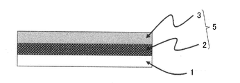
- FIG. 2 It is a section schematic diagram of a transparent electrode.
- A is a perspective view which shows the transparent electrode which concerns on one Embodiment of this invention formed on the board
- substrate (b) is an enlarged view of the transparent electrode part of (a). It is the perspective view which abbreviate
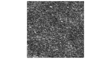
- A) is a perspective view showing each cutting position of the transparent electrode of FIG. 2 (b), and (b) shows a mixed state of the carbon-based material and the conductive oxide in the cross section at each cutting position of (a). It is explanatory drawing shown. It is a surface atomic force microscope (AFM) image of a carbon-type thin film.
- AFM surface atomic force microscope
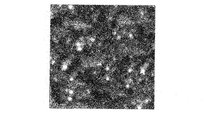
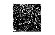
- FIG. 2 is a surface AFM image of a transparent electrode in Example 1.
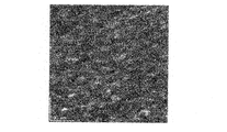
- FIG. 6 is a surface AFM image of a transparent electrode in Comparative Example 1.
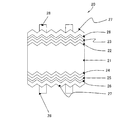
- 10 is a schematic cross-sectional view according to a crystalline silicon solar cell of Example 8.
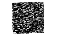
- FIG. 10 is a surface AFM image of a crystalline silicon solar cell of Example 8.
- 7 is a surface AFM image of a crystalline silicon solar cell of Comparative Example 4.
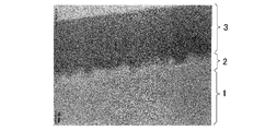
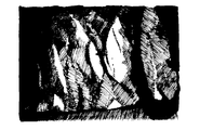
- 10 is a cross-sectional TEM image of the crystalline silicon solar cell of Example 8. It is a graph showing the result of depth direction analysis (Depth Profile). It is the figure which sketched the AFM image of FIG.
- One aspect of the present invention is “a transparent electrode formed on a substrate, wherein the transparent electrode has a carbon-based thin film layer formed on the substrate, and further a transparent conductive compound layer thereon. And a part of the transparent conductive compound layer penetrates into the carbon-based thin film ”.
- the transparent electrode of the present invention is formed on a substrate.
- “formed on the substrate” includes both those formed directly on the substrate and those formed indirectly through other layers. As an example of the latter, one aspect
- a transparent conductive compound typified by an indium oxide-based compound has a film thickness and a conductivity that are substantially proportional, and the conductivity increases as the film thickness increases. It is known that when the film thickness is increased, the crystallinity is improved depending on the film forming process, and the carrier concentration is increased and the mobility is increased. On the other hand, as the film thickness increases, the transparency deteriorates. Thus, since conductivity and transparency are often in a trade-off relationship with each other, it is difficult to achieve both at a high level.
- the inventors focusing on the high carrier concentration of the transparent conductive compound and the high mobility of the carbon-based thin film, the inventors have found a transparent electrode that can achieve high conductivity. Furthermore, since conductivity becomes high, it becomes possible to make a required film thickness thin, and as a result, it becomes possible to improve transparency.
- FIG. 1 shows a typical schematic diagram of the transparent electrode of the present invention.
- the transparent electrode 5 according to an embodiment of the present invention includes a carbon-based thin film layer 2 and a conductive oxide layer 3. Specifically, a carbon-based thin film layer 2 is formed on a substrate (base material) 1 and a transparent conductive compound layer 3 that is a conductive oxide layer is further formed.
- the transparent electrode 5 of this embodiment As shown in FIG. 2, a part of the conductive oxide layer 3 becomes the carbon-based thin film layer 2 in the interface region between the carbon-based thin film layer 2 and the conductive oxide layer 3. It has entered. Specifically, when the transparent electrode 5 is layered in the thickness direction, the substrate 1 side has a carbon-based single region 11 in which only the carbon-based material constituting the carbon-based thin film layer 2 exists, and is on the side far from the substrate 1. Includes a conductive oxide single region 13 in which only the conductive oxide constituting the conductive oxide layer 3 exists. Between these two regions 11 and 13, there is a mixed region 12 in which a carbon-based material and a conductive oxide are mixed.
- the surface of the carbon-based thin film layer 2 on the conductive oxide layer 3 side has irregular irregularities such as clouds and rocks as shown in FIG.
- the mixed region 12 is formed by the conductive oxide layer 3 entering the unevenness.
- the carbon-based thin film layer 2 is hatched in FIGS.
- the abundance ratio of the carbon-based material and the conductive oxide in the mixed region 12 continuously changes from the carbon-based single region 11 to the conductive oxide single region 13.
- the existence ratio does not change stepwise.
- the present invention is not limited to this configuration.
- the abundance ratio changes stepwise in part or all from the carbon-based single region 11 to the conductive oxide single region 13. There may be.
- FIG. 4B schematically shows a cross section of the transparent electrode 5 cut along a plane parallel to the substrate 1 (a plane orthogonal to the thickness direction of the transparent electrode 5). That is, in the AA cross section that cuts the carbon-based single region 11 in the carbon-based thin film layer 2, the abundance ratio of the carbon-based material is 100%. In the DD cross section where the conductive oxide single region 13 in the conductive oxide layer 3 is cut, the abundance ratio of the conductive oxide is 100%.
- both the carbon-based material and the conductive oxide are mixed.
- the abundance ratio of the carbon-based material or the conductive oxide is more than 0% and less than 100%, and the change from 0% to 100% is continuous.
- the abundance ratio of the carbon-based material is more than 0 and less than 50%.
- the abundance ratio of the carbon-based material is 50% or more and less than 100%.
- the cross section obtained by cutting the mixed region 12 along a plane parallel to the substrate 1 includes a cross section containing the carbon-based material and the conductive oxide in a ratio of 3 to 7 to 7 to 3.
- the degree of penetration of the conductive oxide layer 3 into the carbon-based thin film layer 2 is preferably at least half the film thickness of the carbon-based thin film layer 2, but is not limited thereto. It is not a thing. That is, the thickness of the mixed region 22 preferably occupies half or more of the total thickness of the carbon-based thin film layer 2, but may be less than half. In other words, the thickness of the mixed region 22 is preferably larger than the thickness of the carbon-based single region 11, but may be smaller than the thickness of the carbon-based single region 11.
- a transparent electrode 5 is constituted by the carbon-based thin film layer 2 and the transparent conductive compound layer 3.
- the substrate 1 and the transparent electrode 5 constitute a “substrate with a transparent electrode”.
- the base material 1 in the present invention is not particularly limited and can be used properly depending on the application.
- the hard or soft material is not particularly limited.
- the hard material for the base material include single crystal silicon substrates, non-single crystal silicon substrates, oxides such as glass and sapphire, compound semiconductor substrates such as gallium nitride and gallium arsenide, copper-indium-selenium (CIS). ), Copper-indium-gallium-selenium (CIGS), or the like can be used.
- CIS and CIGS cadmium sulfide (CdS), zinc sulfide (ZnS), and zinc oxide (ZnO) may be formed as a buffer layer.
- Specific examples of the glass include alkali glass, borosilicate glass, and non-alkali glass.
- the single crystal or non-single crystal silicon substrate may be intrinsic, but an impurity doped by an ion implantation method or the like can be used.
- crystalline silicon is generally doped p-type or n-type, and conversion efficiency can be improved by using the transparent electrode of the present invention as a transparent electrode on top of this.
- boron is typical
- n-type phosphorus is typical. It can also be used as a transparent electrode of a so-called heterojunction crystalline silicon solar cell in which amorphous silicon is formed on these crystalline silicon substrates.
- the heterojunction crystalline silicon solar cell is, for example, formed by depositing amorphous intrinsic silicon on a single crystal silicon substrate in a thickness of 3 to 200 nm, and further depositing conductive doped amorphous silicon in a thickness of 1 to 30 nm. In addition, a transparent electrode and a collecting electrode are produced.
- the thickness of the single crystal silicon substrate or the non-single crystal silicon substrate may be appropriately selected according to the purpose such as use, but is generally preferably in the range of 80 to 1000 ⁇ m, and more preferably in the range of 100 to 700 ⁇ m.
- the silicon substrate When the silicon substrate is used as a photoelectric conversion layer or a carrier transport layer of a solar cell, a large amount of light can be taken into the photoelectric conversion layer to generate a large amount of current. If the silicon substrate is thin, light sufficient to perform photoelectric conversion may not be captured. Conversely, when the silicon substrate is too thick, carriers generated in the silicon may recombine before reaching the electrode.
- the thickness of the substrate in the case of using glass or sapphire can be arbitrarily selected depending on the purpose of use, but 0.5 to 4.5 mm can be exemplified as a preferable range in consideration of the balance between handling and weight. If the substrate such as glass is too thin, the strength is insufficient, so that it tends to break easily due to impact. On the other hand, if the thickness is too large, the weight becomes heavy and the thickness of the device is affected. Therefore, it is difficult to use the portable device, and it is not preferable in terms of transparency and cost.
- examples of the soft material for the substrate include thermoplastic resins and thermosetting resins.
- examples of the thermoplastic resin include acrylic resin, polyester, polycarbonate resin, polyolefin, and cycloolefin polymer.
- examples of the thermosetting resin include polyurethane.
- a substrate mainly composed of a cycloolefin polymer (COP) having particularly excellent optical isotropy and water vapor blocking properties is preferable.
- COP include norbornene polymers, copolymers of norbornene and olefins, and polymers of unsaturated alicyclic hydrocarbons such as cyclopentadiene.
- the main chain and side chain of the constituent molecules do not contain a functional group having a large polarity, such as a carbonyl group or a hydroxyl group.
- a functional group having a large polarity such as a carbonyl group or a hydroxyl group.
- PEN polyethylene naphthalate
- PES polyethersulfone
- the thickness of the base material using these soft materials can be arbitrarily selected depending on the purpose of use, and is preferably about 0.03 mm to 3.0 mm. If the thickness of the substrate is thin, handling is difficult and the strength is insufficient. On the other hand, if the thickness is large, there are problems in transparency and cost, and the thickness of the device increases, so that it tends to be difficult to use for portable devices.
- a layer for providing a role as an optical design or a base layer may be formed.
- These layers include low-conductivity layers such as silicon oxide, zirconium oxide, hafnium oxide, aluminum oxide, and gallium oxide, and wide gap semiconductor layers such as niobium oxide, titanium oxide, zinc oxide, indium oxide, and tin oxide. Can be mentioned. By adding these layers, it is possible to suppress the reflection of light at the interface from the viewpoint of the difference in refractive index, and it is possible to promote the growth of the carbon-based thin film layer 2 as an underlayer.
- the carbon-based thin film layer 2 is a layer made of a compound containing carbon as a main component.
- FIG. 5 is an atomic force microscope (AFM) image from the surface of the carbon-based thin film
- FIG. 6 is a cross-sectional transmission electron microscope (TEM) image.
- a layer adjacent to the carbon-based thin film layer 2 is a substrate (base material) 1.
- the black layer located on the carbon-based thin film layer 2 is the conductive oxide layer 3. From FIG. 6, it can be confirmed that a part of the conductive oxide layer 3 enters the carbon-based thin film layer 2. Although it seems that a part of the conductive oxide layer 3 has reached the substrate 1, this is a problem in photographing technology and has not actually reached.
- the carbon-based thin film layer in the present invention preferably contains an aggregate of particulate and / or plate-like carbon compounds. This means that a structure having a large gap is formed in the layer. Therefore, when the transparent conductive compound layer 3 is formed, the transparent conductive compound enters the gaps in the carbon-based thin film, and the transparent conductive compound layer is single. The conductivity can be improved as compared with the layer.
- the degree of penetration of the transparent conductive compound layer 3 into the carbon-based thin film layer 2 is determined by the observation of the cross section by TEM, the element in the depth direction, such as secondary ion mass spectrometry (SIMS) or X-ray photoelectron spectroscopy (XPS). This can be confirmed by conducting an analysis.
- SIMS secondary ion mass spectrometry
- XPS X-ray photoelectron spectroscopy
- the transparent electrode of the present invention a part of the conductive oxide layer enters the carbon-based thin film layer.
- the transparent electrode of the present invention has high conductivity.
- the conductive compound supplies the conductive carrier
- the carbon of the carbon-based thin film assists the movement of the conductive carrier.
- carrier scattering at the crystal grain boundary causes a decrease in conductivity.
- the presence of a carbon layer at the crystal grain boundary causes scattering at the crystal grain boundary. It is considered that the carrier to be taken out can be taken out to the carbon-based thin film side.
- the carbon-based thin film layer can be a growth nucleus of the transparent conductive oxide layer.
- the carbon-based thin film layer can be a growth nucleus of the transparent conductive oxide layer.
- the conductivity can be improved, and at the same time, the dopant becomes active by substituting the target site, and the amount of carriers can be increased.
- the activation of conductivity due to ionization of metal in the transparent electrode layer can be considered as a cause of improving the conductivity.
- conductive carriers electrospray carriers
- XPS X-ray photoelectron spectroscopy
- particulate and / or plate-like carbon compounds include fullerenes, carbon nanotubes, graphene, carbon nanowalls, and the like, but are not limited to these compounds. You may not have).
- the carbon-based thin film layer 2 may have a form in which the particulate or plate-like carbon-based compound is present in amorphous carbon.
- the carbon-based thin film layer 2 may contain hydrogen or oxygen in addition to carbon. This is entered depending on the film forming conditions, and there is no problem in characteristics if both elements are 40 atomic% or less.
- the carbon-based thin film layer 2 can be produced by general vapor deposition growth. Examples thereof include a sputtering method, a chemical vapor deposition (CVD) method, a vapor deposition method, and a pulse laser deposition (PLD) method. Among them, the sputtering method and the CVD method are advantageous in terms of excellent productivity because a large area can be easily formed.
- the film can be formed by using carbon as a target, using argon as a carrier gas, and further adding 2 to 40% by volume of carbon dioxide or oxygen. .
- the refractive index can be controlled by adding hydrogen to the reaction system.
- any power source such as a direct current (DC) power source or a low frequency / high frequency power source can be used.
- the carbon-based thin film layer necessary for the present invention can be formed.
- the carbon-based thin film layer 2 is produced by the CVD method, it can be produced by arbitrarily selecting and mixing hydrocarbon gas, carbon dioxide, and hydrogen as source gases.
- the hydrocarbon gas include those obtained by heating and vaporizing aliphatic hydrocarbons such as methane, ethane, and propane, and aromatic hydrocarbons such as benzene.
- the film thickness of the carbon-based thin film layer 2 is preferably 1 to 50 nm, and more preferably 2 to 30 nm. Since the carbon-based thin film has a porous structure, physical strength such as scratch resistance may be lowered if the film thickness is too thick.
- the refractive index of the carbon-based thin film according to the present invention is preferably 1.2 to 1.6 at a wavelength of 500 nm. Furthermore, 1.3 to 1.5 is preferable. From the viewpoint of being able to enter the transparent conductive oxide as described above and become a growth nucleus, a favorable transparent electrode can be produced in the above range.
- the refractive index can be determined by, for example, ellipsometry measurement. In detail, it can obtain
- Refractive index and density have a correlation, and those having a low refractive index generally have a low density.
- the refractive index is in the above range, the carbon-based thin film has a rough structure, and a conductive oxide enters the carbon-based thin film, so that improvement in conductivity can be expected.
- the refractive index is lower than the above range, the density of the carbon-based thin film is too small, and there is a tendency that there is no effect on improving the conductivity.
- the refractive index is larger than the above range, the density of the carbon-based thin film increases, and the conductive oxide does not enter the carbon-based thin film, and the effect of improving the conductivity tends to be difficult to obtain.
- the transparent conductive compound layer 3 in the present invention is made of a transparent conductive oxide.
- the transparent conductive oxide is preferably employed from the viewpoint of uniform film formation with a large area and physical strength and durability.
- Examples of the transparent conductive oxide include oxides of one or more metals selected from zinc, indium, tin, tungsten, titanium, molybdenum, niobium, and the like. More preferably, an oxide of one or more metals selected from zinc, indium, and tin is used. These oxides can be used alone or as a plurality of composite oxides.
- the transparent conductive compound layer 3 can be produced by a known method. Examples include sputtering, metal organic chemical vapor deposition (MOCVD), thermal CVD, plasma CVD, molecular beam epitaxy (MBE), and pulsed laser deposition (PLD).
- MOCVD metal organic chemical vapor deposition
- MBE molecular beam epitaxy
- PLD pulsed laser deposition
- a conductive doping agent can be added to the above metal oxide.
- aluminum, gallium, boron, silicon, carbon, or the like can be added to zinc oxide.
- Zinc, tin, titanium, tungsten, molybdenum, silicon, or the like can be added to indium oxide.
- Fluorine or the like can be added to tin oxide.
- the transparent conductive compound layer 3 can also be constituted by an organic conductive compound or a polymer conductive compound.
- the “substrate with a transparent electrode” in which the transparent electrode of the present invention is formed on a glass substrate or a soft material having a high softening (melting) temperature may be annealed to increase conductivity and light transmittance. it can.
- the annealing atmosphere is preferably a vacuum or an inert gas stream.
- the transparent conductive compound may be thermally oxidized and the conductivity may be reduced.
- the annealing temperature is not less than the temperature at which the crystallinity of zinc oxide is improved, and is preferably not more than the melting temperature of the substrate, specifically about 200 to 450 ° C. By annealing at, an excellent substrate with a transparent electrode can be produced.
- the film thickness of the transparent conductive compound layer 3 is preferably in the range of 100 to 5000 mm (10 to 500 nm), more preferably in the range of 150 to 2000 mm (15 to 200 nm).
- a transparent conductive compound layer having a film thickness in this range a substrate with a transparent electrode having both high transparency and conductivity can be produced.
- the transparent conductive compound layer may be striped and may not be a film.
- the film thickness of the transparent conductive compound layer is increased, light absorption by the transparent conductive compound is increased and the transmittance is decreased, and cracks are likely to occur in the transparent conductive compound layer due to stress.
- the method for detecting the doping amount contained in the transparent conductive compound layer 3 may be any method as long as it is a method usually used for elemental analysis.
- elemental analysis for example, atomic absorption analysis, fluorescent X-ray analysis, etc. Elemental analysis means, X-ray photoelectron spectroscopy, Auger electron spectroscopy, electron beam microanalyzer, and other techniques such as secondary ion mass spectrometry can be used.
- EDX energy dispersive X-ray fluorescence analysis
- SEM scanning electron microscope
- TEM transmission electron microscope
- the surface resistance of the substrate with a transparent electrode to be produced varies depending on the intended use, but can generally be used in the range of 5 to 2500 ⁇ / ⁇ .
- the crystalline silicon solar cell of the present invention includes the transparent electrode of the present invention.
- a single conductivity type single crystal silicon substrate is used as a base material, a p-type silicon-based thin film layer is provided on one surface of the base material, and substantially between the base material and the p-type silicon-based thin film layer.
- a transparent electrode is provided on the p-type silicon thin film layer and the n-type silicon thin film layer, and a collector electrode is provided on the transparent electrode.
- the thickness of the one conductivity type single crystal silicon substrate is 250 ⁇ m or less.
- a single crystal silicon substrate contains an impurity that supplies electric charge to silicon in order to provide conductivity.
- single crystal silicon substrates are generally classified into an n-type that supplies phosphorus atoms that introduce electrons into Si atoms and a p-type that supplies boron atoms that introduce holes (also referred to as holes).
- the heterojunction on the incident side is preferably a reverse junction.
- the single crystal silicon semiconductor substrate used in the present invention is preferably an n-type single crystal silicon semiconductor substrate.
- the reflection layer means a layer that adds a function of reflecting light to the solar cell.
- a metal layer such as Ag or Al may be used, and white high reflection made of metal oxide fine particles such as MgO, Al 2 O 3 , and white zinc. You may form using a material.
- dielectric layers with different refractive indexes and film thicknesses, a multilayer film is formed, and the reflected light at the interface in the multilayer film is interfered with, so that light with a certain range of wavelengths can be detected.
- a photonic structure having reflectivity may be formed.
- a ceramic material or a dielectric layer since the material is an insulator, it is preferable to form the reflective layer after forming the collector electrode on the conductive oxide.
- a preferred configuration of the present invention is a protective layer / collector electrode / transparent electrode layer / n-type amorphous silicon-based thin film.
- the incident surface be an n-layer from the viewpoint of high efficiency recovery of carriers with the reverse junction as the light incident side.
- the incident surface of the single crystal silicon substrate is preferably cut out so as to be a (100) plane.
- a texture structure can be easily formed by anisotropic etching with different etching rates of the (100) plane and the (111) plane.
- the texture size increases as the etching progresses. For example, when the etching time is lengthened, the texture size increases, but the texture size can also be increased by increasing the etchant concentration, the supply rate, and the liquid temperature so as to increase the reaction rate.
- the texture size generally differs between the surface on which the process such as rubbing is performed and the surface on which the process is not performed. Also, in the sharp valleys of the texture formed on the substrate surface, defects are likely to occur due to compressive stress when forming a thin film, so the process of relaxing the shape of the texture valleys and peaks formed after texture formation etching It is preferable to perform isotropic etching with low selectivity on the (100) plane and the (111) plane.
- a method for forming a silicon-based thin film on the single crystal silicon substrate thus manufactured it is particularly preferable to use a plasma CVD method.
- a substrate temperature of 100 to 300 ° C., a pressure of 20 to 2600 Pa, and a high frequency power density of 0.003 to 0.5 W / cm 2 are preferably used.
- a silicon-containing gas such as SiH 4 or Si 2 H 6 or a mixture of these gases and H 2 is preferably used.
- the dopant gas for forming the p-type or n-type layer of the silicon-based thin film in the photoelectric conversion unit for example, B 2 H 6 or PH 3 is preferably used. Further, since the addition amount of impurities such as P and B may be small, a mixed gas diluted with SiH 4 or H 2 in advance can also be used. Further, by adding a gas containing a different element such as CH 4 , CO 2 , NH 3 , GeH 4 or the like to the gas, it is possible to alloy and change the energy gap.
- a p-type silicon thin film layer is provided on one surface of the single crystal silicon substrate, and substantially genuine silicon is provided between the single crystal silicon substrate and the p type silicon thin film layer.
- the system thin film layer is provided.
- the substantially genuine i-type silicon thin film layer is preferably i-type hydrogenated amorphous silicon composed of silicon and hydrogen.
- i-type hydrogenated amorphous silicon layer is formed by CVD, passivation of the single crystal silicon surface can be effectively performed while suppressing impurity diffusion to the single crystal silicon substrate. Further, by changing the amount of hydrogen in the film, it is possible to give an effective profile to the carrier recovery in the energy gap.
- the p-type silicon thin film layer is preferably a p-type hydrogenated amorphous silicon layer or a p-type oxidized amorphous silicon layer. From the viewpoint of impurity diffusion and series resistance, it is preferable to use a p-type hydrogenated amorphous silicon layer for the p-type silicon thin film layer. On the other hand, a p-type oxidized amorphous silicon layer can also be used as a wide gap low refractive index layer from the viewpoint of reducing optical loss.
- n-type silicon thin film layer for example, an n-type hydrogenated amorphous silicon layer, an n-type amorphous silicon nitride layer, and an n-type microcrystalline silicon layer are preferable.
- n-type hydrogenated amorphous silicon that does not contain a crystallization-inhibiting element as the underlayer of the n-type microcrystalline silicon thin film.
- the n-type microcrystalline silicon-based thin film layer include an n-type microcrystalline silicon layer, an n-type microcrystalline silicon carbide layer, and an n-type microcrystalline silicon oxide layer.
- n-type microcrystalline silicon layer to which no impurity is positively added is preferable.
- the n-type microcrystalline silicon layer is provided because the crystallinity of the transparent electrode layer formed thereon can be improved as compared with the case where it is formed on the n-type amorphous silicon layer. It is preferable.
- the n-type silicon thin film layer of the present invention is preferably composed of an n-type hydrogenated amorphous silicon thin film layer and an n-type microcrystalline silicon thin film layer from the i-type silicon thin film layer side.
- the effective optical gap can be widened and the refractive index is lowered, so that optical merit may be obtained.
- the crystalline silicon solar cell of the present invention includes the transparent electrode of the present invention on the p-type and n-type silicon thin film layers.
- the transparent electrode of the present invention includes a carbon-based thin film and a conductive oxide. The detailed description of the transparent electrode of the present invention is as described above.
- the film thickness of the conductive oxide layer in the crystalline silicon solar cell of the present invention is preferably 10 nm or more and 140 nm or less from the viewpoints of transparency and conductivity.
- the role of the conductive oxide layer is to transport carriers to the collector electrode, and it is only necessary to have conductivity necessary for that purpose.
- a conductive oxide layer that is too thick may reduce transmittance due to its own absorption loss, and as a result, may cause a decrease in photoelectric conversion efficiency.
- the resistivity of the transparent electrode layer in the crystalline silicon solar cell of the present invention is preferably 1.8 ⁇ 10 ⁇ 4 ⁇ ⁇ cm or less, more preferably 0.8 ⁇ 10 ⁇ 5 ⁇ ⁇ cm to 1.4 ⁇ . More preferably, it is 10 ⁇ 4 ⁇ ⁇ cm.
- the origin of these conductivities is generally due to free electron drift or diffusion, and substances with such free electrons are reflected by free electrons at wavelengths of 1000 nm and above according to the classic Drude law. ⁇ Absorption occurs. For this reason, if the resistivity is too low, the transmittance on the long wavelength side may be significantly reduced. On the other hand, if the resistivity is too high, it is necessary to increase the number of collector electrodes or increase the film thickness of the transparent electrode. is there.
- the substrate temperature during the production of the transparent electrode layer in the crystalline silicon solar cell of the present invention is preferably 150 ° C. or lower.
- the low temperature side may be, for example, room temperature, but 50 ° C. or higher is preferable because adhesion at the interface of the silicon semiconductor layer / carbon thin film / conductive oxide layer tends to be improved.
- a collector electrode can be formed on the transparent electrode layer.
- the collector electrode can be produced by a known technique such as ink jet, screen printing, conductive wire bonding, spraying, etc., but screen printing is more preferable from the viewpoint of productivity.
- screen printing a process of forming a collecting electrode by printing a conductive paste composed of metal particles and a resin binder by screen printing is preferably used.
- the cell may be annealed also to solidify the conductive paste used for the collector electrode. Annealing also improves each interface characteristic such as improvement of the transmittance / resistivity ratio of the conductive oxide layer and reduction of contact resistance and interface state.
- the annealing temperature is preferably kept in a high temperature region around 100 ° C. from the deposition temperature of the silicon-based thin film. If the annealing temperature is too high, dopant diffusion from the conductive silicon thin film layer to the intrinsic silicon thin film layer, formation of impurity levels due to diffusion of different elements from the conductive oxide layer to the silicon region, amorphous silicon The characteristics may deteriorate due to the formation of defect levels therein.
- a film such as ethylene vinyl acetate (EVA) resin as a protective layer on these layers, it is possible to improve physical strength. Furthermore, it can also serve to prevent deterioration of the silicon layer and electrode layer due to oxygen and moisture. Further, it is possible to suppress loss of optical characteristics by performing blasting or the like having haze on the EVA film. A well-known thing can be used as said protective layer.
- EVA ethylene vinyl acetate
- a resistivity meter Loresta GP MCT-610 (manufactured by Mitsubishi Chemical Corporation) was used for the surface resistance measurement.
- a spectroscopic ellipsometer VASE (manufactured by JA Woollam Co., Ltd.) was used to measure the film thickness of the transparent conductive oxide layer. Fitting was performed using the Chaucy model.
- H-7650 (manufactured by Hitachi, Ltd.) was used as the transmission electron microscope.
- JSPM-4200 manufactured by JEOL Ltd.
- Example 1 A carbon-based thin film was formed to a thickness of 10 nm on an intrinsic silicon substrate.
- the film formation conditions were as follows: the substrate temperature was room temperature, carbon was used as the target, argon and carbon dioxide were used as the carrier gases, 80 sccm and 20 sccm, respectively, and a power density of 0.5 W / cm 2 was applied at a pressure of 8.0 Pa.
- a film was formed. When the surface of this carbon-based thin film was observed with AFM, it was observed as an aggregate of particles (FIG. 5).
- a 50 nm thick indium-zinc composite oxide (IZO: containing 10% by weight of zinc oxide) was formed thereon as a transparent conductive oxide layer.
- IZO indium-zinc composite oxide
- the film forming conditions were as follows: the substrate temperature was room temperature, indium-zinc composite oxide (IZO: containing 10% by weight of zinc oxide) was used as a target, argon was used as a carrier gas at 100 sccm, and the pressure was 0.2 W at a pressure of 0.2 Pa. A film was formed by applying a power density of / cm 2 .
- IZO indium-zinc composite oxide
- argon was used as a carrier gas at 100 sccm
- the pressure was 0.2 W at a pressure of 0.2 Pa.
- a film was formed by applying a power density of / cm 2 .
- the sheet resistance of the transparent electrode thus prepared was measured and found to be 50 ⁇ / ⁇ .
- the shape of the carbon-based thin film was traced (FIG. 7). That is, a dark part exists in a part of FIG. 7, and it is expected that the voids of the carbon-based thin film are traced as they are.
- IZO entered the carbon-based thin film.
- Example 2 A 5 nm niobium oxide layer was formed on alkali-free glass (trade name OA-10, manufactured by Nippon Electric Glass Co., Ltd.).
- the film forming conditions were as follows: the substrate temperature was room temperature, niobium oxide was used as a target, argon and oxygen were used as carrier gases at 70 sccm and 30 sccm, respectively, and a power density of 0.5 W / cm 2 was applied at a pressure of 0.2 Pa.
- a film was formed.
- a carbon-based thin film was formed thereon with a thickness of 10 nm.
- the film formation conditions were as follows: the substrate temperature was room temperature, carbon was used as the target, argon and carbon dioxide were used as the carrier gases, 80 sccm and 20 sccm, respectively, and a power density of 0.5 W / cm 2 was applied at a pressure of 8.0 Pa. A film was formed. When the surface structure of the carbon-based thin film was confirmed by AFM, it was observed as an aggregate of particles. A 50 nm thick indium-zinc composite oxide (IZO: containing 10% by weight of zinc oxide) was formed thereon as a transparent conductive oxide layer.
- IZO indium-zinc composite oxide
- the film forming conditions were as follows: the substrate temperature was room temperature, indium-zinc composite oxide (IZO: containing 10% by weight of zinc oxide) was used as a target, argon was used as a carrier gas at 100 sccm, and the pressure was 0.2 W at a pressure of 0.2 Pa. A film was formed by applying a power density of / cm 2 .
- IZO indium-zinc composite oxide
- argon was used as a carrier gas at 100 sccm
- the pressure was 0.2 W at a pressure of 0.2 Pa.
- a film was formed by applying a power density of / cm 2 .
- the sheet resistance of the transparent electrode thus produced was measured and found to be 55 ⁇ / ⁇ .
- Example 3 A transparent electrode was produced in the same manner except that IZO of Example 1 was changed to indium-tungsten composite oxide (IWO: containing 1 wt% of tungsten oxide).
- the sheet resistance of the transparent electrode thus produced was measured and found to be 55 ⁇ / ⁇ .
- Example 4 A transparent electrode was prepared in the same manner except that IZO of Example 1 was changed to indium-tin composite oxide (ITO: containing 10% by weight of tin oxide).
- ITO indium-tin composite oxide
- the sheet resistance of the transparent electrode thus produced was measured and found to be 45 ⁇ / ⁇ .
- Example 5 A transparent electrode was produced in the same manner except that IZO of Example 1 was changed to an indium-titanium composite oxide (ITO: containing 1% by weight of titanium oxide).
- ITO indium-titanium composite oxide
- the sheet resistance of the transparent electrode thus prepared was measured and found to be 60 ⁇ / ⁇ .
- Example 6 A transparent electrode was produced in the same manner except that IZO of Example 1 was changed to indium-molybdenum composite oxide (IMO: containing 1% by weight of molybdenum oxide).
- IMO indium-molybdenum composite oxide
- the sheet resistance of the transparent electrode thus prepared was measured and found to be 58 ⁇ / ⁇ .
- Example 7 A transparent electrode was prepared in the same manner except that the thickness of the carbon-based thin film of Example 1 was 60 nm.
- the cross-sectional TEM of the carbon-based thin film thus produced was measured, it was a structure in which the plate-like ones overlapped (FIG. 6).
- the sheet resistance of the transparent electrode thus produced was 52 ⁇ / ⁇ .
- indium-zinc composite oxide (IZO: containing 10% by weight of zinc oxide) was formed as a transparent conductive oxide layer on an intrinsic silicon substrate to a thickness of 50 nm.
- the film forming conditions were as follows: the substrate temperature was room temperature, indium-zinc composite oxide (IZO: containing 10% by weight of zinc oxide) was used as a target, and argon gas was used as a carrier gas at 100 sccm at a pressure of 0.2 Pa.
- a film was formed by applying a power density of 5 W / cm 2 .
- the sheet resistance of the transparent electrode thus produced was measured and found to be 120 ⁇ / ⁇ .
- AFM AFM
- Example 2 An indium-zinc composite oxide (IZO: containing 10% by weight of zinc oxide) was deposited on an alkali-free glass as a transparent conductive oxide layer to a thickness of 50 nm.
- the film forming conditions were as follows: the substrate temperature was room temperature, indium-zinc composite oxide (IZO: containing 10% by weight of zinc oxide) was used as a target, and argon gas was used as a carrier gas at 100 sccm at a pressure of 0.2 Pa.
- a film was formed by applying a power density of 5 W / cm 2 .
- the sheet resistance of the transparent electrode thus prepared was measured and found to be 150 ⁇ / ⁇ .
- niobium oxide layer was formed on alkali-free glass.
- the film forming conditions were as follows: the substrate temperature was room temperature, niobium oxide was used as a target, argon and oxygen were used as carrier gases at 70 sccm and 30 sccm, respectively, and a power density of 0.5 W / cm 2 was applied at a pressure of 0.2 Pa. A film was formed. A 50 nm thick indium-zinc composite oxide (IZO: containing 10% by weight of zinc oxide) was formed thereon as a transparent conductive oxide layer.
- IZO indium-zinc composite oxide
- the film forming conditions were as follows: the substrate temperature was room temperature, indium-zinc composite oxide (IZO: containing 10% by weight of zinc oxide) was used as a target, and argon gas was used as a carrier gas at 100 sccm at a pressure of 0.2 Pa. A film was formed by applying a power density of 5 W / cm 2 .
- IZO indium-zinc composite oxide
- argon gas was used as a carrier gas at 100 sccm at a pressure of 0.2 Pa.
- a film was formed by applying a power density of 5 W / cm 2 .
- the sheet resistance of the transparent electrode thus prepared was measured and found to be 150 ⁇ / ⁇ .
- FIG. 9 is a schematic cross-sectional view showing a crystalline silicon-based solar cell 20 of Example 8 according to the present invention.
- the crystalline silicon solar cell 20 of the present embodiment is a heterojunction solar cell, and has a texture on both sides of the n-type single crystal silicon substrate 21.
- an i-type amorphous silicon layer 22 / p-type amorphous silicon layer 23 / carbon-based thin film 26 is formed on the incident surface of the n-type single crystal silicon substrate 21, an i-type amorphous silicon layer 22 / p-type amorphous silicon layer 23 / carbon-based thin film 26 is formed.
- a conductive oxide layer 27 is formed thereon, and a collector electrode 28 is formed thereon.
- an i-type amorphous silicon layer 24 / n-type amorphous silicon layer 25 / carbon-based thin film 26 is formed on the back surface of the substrate 21. Further, a conductive oxide layer 27 is formed thereon, and a collector electrode 28 is formed thereon.
- a crystalline silicon solar cell 20 of Example 8 shown in FIG. 9 was produced as follows.
- n-type single crystal silicon substrate having an incident plane of (100) and a thickness of 200 ⁇ m was washed in acetone, then immersed in a 2 wt% HF aqueous solution for 3 minutes to remove the silicon oxide film on the surface, The rinse with ultrapure water was performed twice.
- the substrate was dipped in a 5/15 wt% KOH / isopropyl alcohol aqueous solution maintained at 70 ° C. for 15 minutes, and a texture was formed by etching the substrate surface. Thereafter, rinsing with ultrapure water was performed twice.
- the surface of the single crystal silicon substrate 11 was observed with an atomic force microscope (AFM manufactured by Pacific Nanotechnology Co., Ltd.), the substrate surface was most etched and a pyramidal texture with an exposed (111) plane was formed. It had been.
- AFM atomic force microscope
- the single crystal silicon substrate 21 was introduced into a CVD apparatus, and an i-type amorphous silicon layer 22 was formed to a thickness of 3 nm on the incident surface.
- the film thickness of the thin film formed in this example was measured by spectroscopic ellipsometry (trade name VASE, manufactured by JA Woollam Co., Ltd.) when the film was formed on a glass substrate under the same conditions.
- the film forming speed was obtained and calculated on the assumption that the film was formed at the same film forming speed.
- the film forming conditions for the i-type amorphous silicon layer 22 were a substrate temperature of 150 ° C., a pressure of 120 Pa, a SiH 4 / H 2 flow rate ratio of 3/10, and an input power density of 0.011 W / cm ⁇ 2 .
- a p-type amorphous silicon layer 13 was deposited on the i-type amorphous silicon layer 22 to a thickness of 4 nm.
- the conditions for forming the p-type amorphous silicon layer 23 were as follows: the substrate temperature was 150 ° C., the pressure was 60 Pa, the SiH 4 / B 2 H 6 flow rate ratio was 1/3, and the input power density was 0.01 W / cm ⁇ 2. It was.
- the B 2 H 6 gas used above was a gas diluted with H 2 to a B 2 H 6 concentration of 5000 ppm.
- an i-type amorphous silicon layer 24 was formed to a thickness of 6 nm on the back side.
- the film forming conditions for the i-type amorphous silicon layer 24 were a substrate temperature of 150 ° C., a pressure of 120 Pa, a SiH 4 / H 2 flow rate ratio of 3/10, and an input power density of 0.011 W / cm ⁇ 2 .
- An n-type amorphous silicon layer 25 having a thickness of 4 nm was formed on the i-type amorphous silicon layer 24.
- the film forming conditions for the n-type amorphous silicon layer 25 were a substrate temperature of 150 ° C., a pressure of 60 Pa, a SiH 4 / PH 3 flow rate ratio of 1/2, and an input power density of 0.01 W / cm ⁇ 2 .
- the PH 3 gas used above was a gas diluted with H 2 to a PH 3 concentration of 5000 ppm.
- a carbon-based thin film 26 having a thickness of 10 nm was formed on the p-type amorphous silicon layer 23 and the n-type amorphous silicon layer 25.
- the film forming conditions were as follows: the substrate temperature was 150 ° C., carbon was used as the target, argon and carbon dioxide were used as the carrier gases, 80 sccm and 20 sccm, respectively, and a power density of 0.5 W / cm 2 was applied at a pressure of 8.0 Pa. To form a film.
- the surface of the carbon-based thin film 26 was observed with an AFM, it was observed as an aggregate of particles like FIG.
- the refractive index of the carbon-based thin film 26 measured by spectroscopic ellipsometry was 1.4.
- a 100 nm thick indium-tin composite oxide (ITO: containing 10% by weight of tin oxide) was formed as a conductive oxide layer 27 thereon.
- the film forming conditions were as follows: the substrate temperature was 150 ° C., indium-tin composite oxide (ITO: containing 10% by weight of tin oxide) was used as a target, argon was used as a carrier gas at 100 sccm, and the pressure was 0.2 Pa.
- the film was formed with a power density of 5 W / cm 2 .
- This carbon-based thin film 10 nm and ITO 100 nm were formed on an intrinsic silicon substrate (resistance of 1 ⁇ 10 6 ⁇ / ⁇ or more) under the same conditions as described above. When this resistivity was measured, it was 1.4 ⁇ 10 ⁇ 4 ⁇ ⁇ cm.
- FIG. 10 When the surface of the transparent electrode portion was observed with AFM, the shape of the carbon thin film was traced (FIG. 10). That is, as in Example 1, a dark part was present in part of FIG. 10, and it was expected that the voids of the carbon-based thin film were traced as they were.
- Example 9 A crystalline silicon-based solar cell 20 is produced in the same manner as in Example 8, except that the carbon-based thin film 26 of Example 8 is formed under the conditions of argon, carbon dioxide, and hydrogen of 75 sccm, 20 sccm, and 5 sccm, respectively. did.
- the refractive index of the carbon-based thin film was measured by spectroscopic ellipsometry and found to be 1.5.
- This carbon-based thin film 10 nm and ITO 100 nm were formed on an intrinsic silicon substrate (resistance of 1 ⁇ 10 6 ⁇ / ⁇ or more) under the same conditions. When this resistivity was measured, it was 1.4 ⁇ 10 ⁇ 4 ⁇ ⁇ cm.
- Example 10 A crystalline silicon solar cell 20 was produced in the same manner as in Example 8, except that indium-zinc composite oxide (IZO: containing 10% by weight of zinc oxide) was used as the conductive oxide layer of Example 8. An indium-zinc composite oxide (IZO: containing 10% by weight of zinc oxide) was used as an IZO target.
- indium-zinc composite oxide IZO: containing 10% by weight of zinc oxide
- a carbon-based thin film of 10 nm and IZO of 100 nm were formed on an intrinsic silicon substrate (resistance of 1 ⁇ 10 6 ⁇ / ⁇ or more) under the same conditions as described above. When this resistivity was measured, it was 1.3 ⁇ 10 ⁇ 4 ⁇ ⁇ cm.
- Example 11 A crystalline silicon solar cell 20 was produced in the same manner as in Example 8, except that the conductive oxide layer of Example 8 was zinc-gallium composite oxide (GZO: containing 2% by weight of gallium oxide). As a GZO target, a zinc-gallium composite oxide (GZO: containing 2% by weight of gallium oxide) was used.
- GZO zinc-gallium composite oxide
- the carbon-based thin film 10 nm and GZO 100 nm were formed on an intrinsic silicon substrate (resistance of 1 ⁇ 10 6 ⁇ / ⁇ or more) under the same conditions as described above. When this resistivity was measured, it was 1.4 ⁇ 10 ⁇ 4 ⁇ ⁇ cm.
- Example 8 is the same as Example 8 except that the conductive oxide layer of Example 8 has a thickness of 1500 nm of zinc-boron composite oxide (BZO: containing 2% by weight of boron oxide) and the thickness of the carbon-based thin film is 100 nm.
- BZO zinc-boron composite oxide
- a crystalline silicon solar cell 20 was produced.
- BZO was fabricated using a metal organic chemical vapor deposition (MOCVD) method. Diethylzane and water were used as raw materials, each of which was vaporized at 100 ° C., and three kinds of diborane raw materials diluted with hydrogen to 5000 ppm were charged into the reaction system using hydrogen as a carrier gas.
- the substrate temperature was 150 ° C.
- the deposition chamber was 3.0 Torr.
- a carbon-based thin film of 100 nm and BZO of 1500 nm were formed on an intrinsic silicon substrate (resistance of 1 ⁇ 10 6 ⁇ / ⁇ or more) under the same conditions as described above.
- the resistivity was measured and found to be 1.8 ⁇ 10 ⁇ 4 ⁇ ⁇ cm.
- Example 13 A crystalline silicon solar cell 20 was produced in the same manner as in Example 8 except that indium oxide was used as the conductive oxide layer of Example 8. Indium oxide was used as the target of indium oxide. A carbon-based thin film of 10 nm and indium oxide of 100 nm were formed on an intrinsic silicon substrate (resistance of 1 ⁇ 10 6 ⁇ / ⁇ or more) under the same conditions as described above. When this resistivity was measured, it was 1.5 ⁇ 10 ⁇ 4 ⁇ ⁇ cm.
- Example 14 As the conductive oxide layer of Example 8, an indium-tin composite oxide (ITO: containing 2% by weight of tin oxide) was formed to a thickness of 100 nm.
- the film forming conditions were as follows: the substrate temperature was 150 ° C., indium-tin composite oxide (ITO: containing 2% by weight of tin oxide) was used as a target, argon was used as a carrier gas at 100 sccm, and the pressure was 0.2 Pa.
- the film was formed with a power density of 5 W / cm 2 .
- This carbon-based thin film 10 nm and ITO 100 nm were formed on an intrinsic silicon substrate (resistance of 1 ⁇ 10 6 ⁇ / ⁇ or more) under the same conditions as described above. When this resistivity was measured, it was 1.3 ⁇ 10 ⁇ 4 ⁇ ⁇ cm.
- Example 4 A crystalline silicon solar cell was produced in the same manner as in Example 8 except that no carbon thin film was provided. The interval between the collecting electrodes was 5 mm.
- An ITO 100 nm film was formed on an intrinsic silicon substrate (resistance of 1 ⁇ 10 6 ⁇ / ⁇ or more) under the same conditions as described above.
- the resistivity was measured and found to be 2.4 ⁇ 10 ⁇ 4 ⁇ ⁇ cm.
- FIG. 11 shows a surface AFM image of the transparent electrode portion. Comparing FIG. 10 (Example 8) and FIG. 11 (Comparative Example 4), FIG. 10 was darker. Thereby, the height difference which exists on the carbon-type thin film layer of the transparent electrode of Example 8 was confirmed.
- Comparative Example 5 A crystalline silicon solar cell was produced in the same manner as in Comparative Example 4 except that the distance between the collector electrodes was 10 mm.
- the film forming conditions of the carbon-based thin film 16 were as follows. Using methane as a raw material, a substrate temperature was set to room temperature, a pressure was set to 20 Pa, and an applied power density was formed to a thickness of 70 nm by plasma CVD with an applied power density of 0.1 W / cm 2 . The refractive index of the carbon-based thin film was measured by spectroscopic ellipsometry and found to be 1.7. A crystalline silicon solar cell was produced in the same manner as in Example 8 except for the carbon thin film 26.
- Comparative Example 7 A crystalline silicon solar cell was produced in the same manner as in Comparative Example 6 except that the thickness of the carbon thin film was 10 nm.
- Table 1 shows the short-circuit current (Jsc), open-circuit voltage (Voc), fill factor (FF), and conversion efficiency (Eff) of the solar cell module.
- the short-circuit current was particularly improved by forming a conductive oxide film on a carbon-based thin film as the transparent electrode layer. This is presumably because the conductivity of the transparent electrode layer was improved, so that the interval between the collecting electrodes could be increased, and the amount of light taken up increased. Since the transparent electrode of the comparative example has high resistivity, it is considered that the performance is inferior due to loss of carrier transport.
- the reason why the short-circuit current is smaller in the comparative example 6 than in the example is that the refractive index is amorphous silicon layer> conductive oxide> carbon-based thin film. It is thought to be trapped in. In Comparative Example 7, it was considered that the improvement in characteristics was not observed because the carbon-based thin film did not contribute to the conductivity.
- the ratio of the conductive oxide thin film changed rapidly from 1 to 0.
Landscapes
- Photovoltaic Devices (AREA)
Abstract
太陽電池等に用いられる透明電極について、透明導電膜の膜厚を大きくすることなく導電性を向上させることを課題とする。 基材上に形成された透明電極であって、該透明電極が、基材上に炭素系薄膜層が形成されており、さらにその上に導電性酸化物層が形成されており、且つ該導電性酸化物層はその一部が炭素系薄膜層に入り込んでいることを特徴とする透明電極が提供される。当該透明電極を備えた結晶シリコン系太陽電池も提供される。
Description
本発明は、主として単結晶シリコン系または非単結晶シリコン系太陽電池の透明電極や裏面電極、ハイブリッド型太陽電池の透明中間層、化合物半導体系太陽電池の透明電極、タッチパネルやPDP、LCDやエレクトロルミネッセンス(EL)ディスプレイ材料、化合物半導体高速デバイスに用いる低誘電率膜、表面弾性波素子、赤外線カットなどを目的とした窓ガラスコーティング、ガスセンサー、非線形光学を活用したプリズムシート、透明磁性体、光学記録素子、光スイッチ、光導波路、光スプリッタ、光音響材料、高温発熱ヒーター材料、などの材料において、高い導電性を達成可能な透明電極に関するものである。
また本発明は、単結晶シリコン基板表面にヘテロ接合を有する結晶シリコン系太陽電池に関し、更に詳しくは光電変換効率に優れた結晶シリコン系太陽電池に関するものである。
太陽電池やタッチパネルやディスプレイ材料などに使用される透明電極付き基板は、その透明導電層として酸化インジウム錫(ITO)や酸化錫、酸化亜鉛などが広く使用されている。このような透明導電層は、マグネトロンスパッタリング法やモレキュラービームエピタキシー法などの物理気相堆積法(PVD法)、熱CVDやプラズマCVDなどの化学気相堆積法(CVD法)などにより形成されるほか、無電解法により形成されることが知られている。
中でもITOは透明導電材料として非常に優れた材料であり、現在広く透明導電層に使用されている。しかしながら、原料のインジウムが枯渇する可能性があり、資源的にもコスト的にもITOに替わる材料の探索が急務となっている。
このようなインジウムの原料に関わる問題への対策として、非インジウム材料を使用すること、使用するインジウムの量を減らすことの2つの方法が挙げられる。
例えば、非特許文献1には非インジウム材料として酸化亜鉛を用いた透明導電膜が記載されている。しかし、酸化亜鉛は、水や空気に対する耐久性が乏しく、特に導電率が容易に変化してしまうことが記載されている。
酸化物以外の材料としては、例えば、特許文献1にカーボンナノチューブを用いた電極について記載されている。しかし、カーボンナノチューブは大量に作製することが困難であるためにコストが高くなること、透明性が劣ることから実用化までには至っていない。
一方、特許文献2には、ガリウムやアルミニウムを含む酸化亜鉛とITOを積層することで、ITOの使用量を減少する技術が開示されている。
このようにインジウムの代替材料の研究やインジウムの使用量を減少させる研究は広く行われているが、前者の場合には実用化に対して課題が多く、後者の場合にはインジウムの使用量を減少することができるが導電性の向上などの課題がある。
結晶シリコン基板を用いた結晶シリコン太陽電池は、光電変換効率が高く、既に太陽光発電システムとして広く一般に実用化されている。中でも単結晶シリコンとはバンドギャップの異なる非晶質シリコン系薄膜を単結晶表面へ製膜し、拡散電位を形成した結晶シリコン太陽電池はヘテロ接合太陽電池と呼ばれている。
さらに、中でも拡散電位を形成するための導電型非晶質シリコン系薄膜と結晶シリコン表面の間に薄い真性の非晶質シリコン層を介在させる太陽電池は、変換効率の最も高い結晶シリコン太陽電池の形態の一つとして知られている。結晶シリコン表面と導電型非晶質シリコン系薄膜の間に、薄い真性な非晶質シリコン層を製膜することで、製膜による新たな欠陥準位の生成を低減しつつ結晶シリコンの表面に存在する欠陥(主にシリコンの未結合手)を水素で終端化処理することができる。また、導電型非晶質シリコン系薄膜を製膜する際の、キャリア導入不純物の結晶シリコン表面への拡散を防止することもできる。
近年、結晶シリコン太陽電池の原料問題の観点から使用する単結晶シリコン基板の厚みを低減する必要性が高まっている。このため、この基板の厚みの低減に応じて、光を基板内へ閉じ込める技術が重要となっている。
これに対し、一般的に非晶質シリコンを導電型層として用いるヘテロ接合太陽電池において、入射面と裏面に酸化インジウムを透明電極として用いることが透過率、導電性、電気的接合及び信頼性の観点から良いことが開示されている(例えば、特許文献3参照)。一方で、厚いi層を有する薄膜シリコン太陽電池において、裏面n型層上に製膜する導電性酸化物層として酸化亜鉛を用いる際に、i型微結晶シリコン/n型微結晶シリコン層を導電性酸化物層との界面に配置することが開示されている(例えば、特許文献4参照)。
特許文献5には、屈折率が1.6~2.0の範囲のダイヤモンド様炭素膜が背面電極側に配置されている光起電力素子が開示されている。しかし、この範囲の屈折率のカーボン層は膜が密なアモルファスカーボンである。
特許文献6には透明電極材料として、タングステンをドーピングした酸化インジウムが報告されている。この透明電極材料は100nmの膜厚で抵抗率が3~9×10⁻⁴Ω・cmである。一方、特許文献7に記載の透明電極材料はフッ素をドーピングすることで抵抗率が2.2×10⁻⁴Ω・cmを達成している。さらに非特許文献2では錫をドーピングした酸化インジウムで抵抗率が2.1×10⁻⁴Ω・cmを達成している。
結晶シリコン系太陽電池では透明電極の膜厚は約100nm程度であるが、上記の透明電極のシート抵抗は20Ω/□以上である。しかし、結晶シリコン系太陽電池では、透明電極の上に集電極とバスバーがあり、これが発電のための有効面積を小さくし、モジュールの変換効率を小さくする原因であった。
一方、上記透明電極を用いたまま集電極の占める面積を減らす場合には、透明電極の厚さを厚くして導電率を上げる必要があり、これは透明電極での光吸収ロスの原因となるため、光電変換効率を上げることができなかった。
非特許文献3の10ページには酸化亜鉛への導電性ドーピングにより1.5×1021cm-3のキャリア濃度であり、且つ1.9×10⁻⁴Ω・cmの抵抗率を達成したことが記載されている。しかし、その化学的な不安定さから実用化の障害となっている。
澤田豊 監修、「透明導電膜」、6~19ページ(1999年)(シーエムシー出版)
Japanese Journal of Applied physics,46.L685(2007)
透明導電膜、澤田豊著、シーエムシー出版(2005)
本発明は、良好な導電性を示す透明電極を提供することを目的とする。
また本発明は、結晶シリコン系太陽電池において、光電変換層への光の取り込み量を多くすることで光電変換効率の向上をはかることを目的とする。
上記課題を解決するために、本発明者らは鋭意検討を重ねた結果、導電性ナノカーボン物質に代表される炭素系薄膜上に導電性化合物を製膜することで、導電性化合物の粒界散乱による導電性の低下を抑制し、高導電性の透明電極を作製可能であることを見出した。
また本発明者らは、前記透明電極を用いることによって、結晶シリコン系太陽電池の光電変換効率、特に出力電流の向上が可能であることを見出した。
すなわち本発明の1つの様相は、基材上に形成された透明電極であって、該透明電極が、基材上に炭素系薄膜層が形成されており、さらにその上に透明導電性化合物層が形成されており、且つ該透明導電性化合物層はその一部が炭素系薄膜に入り込んでいることを特徴とする透明電極である。
好ましくは、透明電極を厚さ方向に層別したとき、基材側には炭素系薄膜層を構成する炭素系物質のみが存在する炭素系単独領域があり、基材から遠い側には導電性酸化物層を構成する導電性酸化物のみが存在する導電性酸化物単独領域があり、これら2つの領域の間に、炭素系物質と導電性酸化物とが混在する混在領域がある。
好ましくは、前記混在領域を基材に対して平行な平面で切断した断面には、炭素系物質と導電性酸化物とを3対7から7対3の範囲の割合で含む断面が存在する。
好ましくは、前記炭素系薄膜層が、500nmの波長における屈折率が1.2~1.6のものである。
好ましくは、前記炭素系薄膜層が、粒子状及び/又は板状の炭素物質の集合体から形成される。
好ましくは、前記導電性酸化物層を構成する酸化物が、亜鉛、インジウム、錫、タングステン、チタン、モリブデン、及びニオブからなる群より選択される1種以上の金属の酸化物である。
好ましくは、前記導電性酸化物層を構成する酸化物が、亜鉛、インジウム、及び錫からなる群より選択される1種以上の金属の酸化物である。
本発明の他の様相は、上記した本発明の透明電極を備えたことを特徴とする結晶シリコン系太陽電池である。
好ましくは、一導電型単結晶シリコン基板を基材とし、前記基材の一面にp型シリコン系薄膜層を有し、前記基材と前記p型シリコン系薄膜層との間に実質的に真正なシリコン系薄膜層を備え、前記基材の他面にn型シリコン系薄膜層を有し、前記基材と前記n型シリコン系薄膜層との間に実質的に真正なシリコン系薄膜層を備え、前記p型シリコン系薄膜層上及び前記n型シリコン系薄膜層上に、前記透明電極を備え、前記透明電極上に集電極を設けている。
好ましくは、前記一導電型単結晶シリコン基板の厚みが250μm以下である。
好ましくは、前記透明電極の抵抗率が1.8×10⁻⁴Ω・cm以下である。
本発明の透明電極によれば、太陽電池やタッチパネルやエレクトロルミネッセンス用電極基板などで特に重要な要素である「導電性」において良好な特性を示す透明電極付き基板を提供することが可能となる。
本発明の結晶シリコン型太陽電池によれば、結晶シリコン系太陽電池の各界面における不純物拡散が減少し、さらに各界面どうしの密着性の向上が期待できる。このため、光電変換効率に優れた結晶シリコン系太陽電池を提供できる。
以下、本発明の実施形態について、図面を参照しながら詳細に説明する。なお、以下の説明は、実施形態の理解を容易にするためのものであり、これによって、本発明が制限して理解されるべきではない。
本発明の1つの様相は、「基材上に形成された透明電極であって、該透明電極が、基材上に炭素系薄膜層が形成されており、さらにその上に透明導電性化合物層が形成されており、且つ該透明導電性化合物層はその一部が炭素系薄膜に入り込んでいることを特徴とする透明電極」に関するものである。
本発明の透明電極は基材上に形成されたものである。ここで「基材上に形成」とは、基材上に直接的に形成されたものと、他の層を介して間接的に形成されたものの両方を含む。後者の例としては、後述する本発明の結晶シリコン系太陽電池の一態様が挙げられる。すなわち、本発明の結晶シリコン系太陽電池の一態様においては、一導電型単結晶シリコン基板(基材)と透明電極との間に各種のシリコン系薄膜層を有している。
太陽電池やエレクトロルミネッセンス照明デバイス、タッチパネルなどに用いられる透明電極において、重要な要素として「導電性」と「透明性」がある。通常、酸化インジウム系化合物に代表される透明導電性化合物は、その膜厚と導電性がほぼ比例しており、膜厚が厚くなると導電性が向上する。これは、膜厚が厚くなると製膜工程によっては結晶性が向上し、キャリア濃度の上昇と移動度の向上が起こるためであることが知られている。一方で膜厚が厚くなると透明性が悪くなる。このように、導電性と透明性は互いにトレードオフの関係にあることが多いため、両方を高いレベルで達成することは困難である。
本発明では、透明導電性化合物の高キャリア濃度、炭素系薄膜の高移動度に着目し、導電性を高いレベルで達成可能な透明電極を見出した。さらに導電性が高くなることで、必要な膜厚を薄くすることが可能となるので、結果として透明性を向上することが可能となる。
以下、本発明に係る透明電極の代表的な態様を説明する。
図1に本発明の透明電極の代表的な模式図を示している。図1に示すように、本発明の一実施形態に係る透明電極5は、炭素系薄膜層2と導電性酸化物層3とからなる。詳細には、基板(基材)1上に炭素系薄膜層2が形成され、さらに導電性酸化物層である透明導電性化合物層3が形成されてなるものである。
本実施形態の透明電極5においては、図2に示すように、炭素系薄膜層2と導電性酸化物層3の界面領域において、導電性酸化物層3の一部が炭素系薄膜層2に入り込んでいる。詳細には、透明電極5を厚さ方向に層別したとき、基板1側には炭素系薄膜層2を構成する炭素系物質のみが存在する炭素系単独領域11があり、基板1から遠い側には導電性酸化物層3を構成する導電性酸化物のみが存在する導電性酸化物単独領域13がある。そして、これら2つの領域11,13の間に、炭素系物質と導電性酸化物とが混在する混在領域12がある。
炭素系薄膜層2における導電性酸化物層3側の面は、図3に示すように、雲や岩石の如く不規則な凹凸を有している。この凹凸に導電性酸化物層3が入り込むことで、混在領域12が形成されている。
なお、理解を容易にするために、図2~4において、炭素系薄膜層2にはハッチングを施している。
炭素系薄膜層2における導電性酸化物層3側の面は、図3に示すように、雲や岩石の如く不規則な凹凸を有している。この凹凸に導電性酸化物層3が入り込むことで、混在領域12が形成されている。
なお、理解を容易にするために、図2~4において、炭素系薄膜層2にはハッチングを施している。
本実施形態においては、混在領域12における炭素系物質と導電性酸化物の存在比率が、炭素系単独領域11から導電性酸化物単独領域13に至る間で連続的に変化する。換言すれば、前記存在比率は、段階的には変化しない。ただし本発明はこの構成に限定されるものではなく、例えば、炭素系単独領域11から導電性酸化物単独領域13に至る間の一部又は全部において、前記存在比率が段階的に変化するものであってもよい。
図4(b)は、透明電極5を、基板1に対して平行な平面(透明電極5の厚み方向に直交する平面)で切断した断面を模式的に表している。すなわち、炭素系薄膜層2における炭素系単独領域11を切断するA-A断面では、炭素系物質の存在比率が100%である。また、導電性酸化物層3における導電性酸化物単独領域13を切断するD-D断面では、導電性酸化物の存在比率が100%である。
一方、混在領域12を切断した切断面では、炭素系物質と導電性酸化物の両方が混在する。混在領域12においては、炭素系物質あるいは導電性酸化物の存在比率が0%を超え100%未満であり、かつ0%から100%への変化は連続的である。例えば、より基板1側に近いB-B断面では、炭素系物質の存在比率が0を超え50%未満である。基板1から遠い側のC-C断面では、炭素系物質の存在比率が50%以上100%未満である。
好ましくは、混在領域12を、基板1に対して平行な平面で切断した断面は、炭素系物質と導電性酸化物とを3対7から7対3の範囲の割合で含む断面が存在する。換言すれば、前記断面において、炭素系物質あるいは導電性酸化物の存在比率が30%から70%の範囲である断面が、少なくとも1つ存在する。
好ましくは、混在領域12を、基板1に対して平行な平面で切断した断面は、炭素系物質と導電性酸化物とを3対7から7対3の範囲の割合で含む断面が存在する。換言すれば、前記断面において、炭素系物質あるいは導電性酸化物の存在比率が30%から70%の範囲である断面が、少なくとも1つ存在する。
なお、導電性酸化物層3の炭素系薄膜層2への入り込み度合いについては、導電性酸化物層3が炭素系薄膜層2の膜厚の半分以上であることが好ましいが、それに限定されるものではない。すなわち、混在領域22の厚みは、炭素系薄膜層2全体の厚みの半分以上を占めることが好ましいが、半分未満でもかまわない。さらに換言すれば、混在領域22の厚みは、炭素系単独領域11の厚みより大きいことが好ましいが、炭素系単独領域11の厚みより小さくてもかまわない。
炭素系薄膜層2と透明導電性化合物層3によって、透明電極5が構成される。また、基板1と透明電極5によって、「透明電極付き基板」が構成される。
本発明における上記基材1については、用途によって使い分けられるものであり、特に限定されない。透明電極の基材として使用する場合には、硬質または軟質材料は特に限定されない。例えば、前記基材用の硬質材料としては、単結晶シリコン基板、非単結晶シリコン基板、ガラス、サファイヤなどの酸化物や窒化ガリウムやヒ化ガリウムなどの化合物半導体基板、銅-インジウム-セレン(CIS)や銅-インジウム-ガリウム-セレン(CIGS)などを用いることができる。これらのCISやCIGS上にはバッファー層として硫化カドミウム(CdS)や硫化亜鉛(ZnS)、酸化亜鉛(ZnO)を製膜しても良い。ガラスの具体例としては、アルカリガラスやホウ珪酸ガラス、無アルカリガラスなどがあげられる。
前記単結晶または非単結晶シリコン基板は真性であってもよいが、イオン注入法などにより不純物をドーピングしたものを用いることができる。結晶シリコン系太陽電池では結晶シリコンはp型またはn型にドーピングされているものが一般的であり、この上に透明電極として本発明の透明電極を使用することで変換効率の向上が可能となる。ドーピングは、p型であればホウ素が代表的であり、n型であればリンが代表的である。またこれらの結晶シリコン基板上に非晶質シリコンを製膜した、いわゆるヘテロ接合型結晶シリコン系太陽電池の透明電極としても使用することができる。ヘテロ接合型結晶シリコン系太陽電池は、例えば、単結晶シリコン基板に非晶質の真性シリコンを3~200nm製膜し、さらに導電性ドーピングされた非晶質シリコンを1~30nm製膜されたものに、透明電極、集電極を作製したものである。
前記の単結晶シリコン基板または非単結晶シリコン基板の厚みは、用途等目的に応じて適宜選択すればよいが、概して80~1000μmの範囲が好ましく、さらには100~700μmの範囲が好ましい。
前記シリコン基板を太陽電池の光電変換層やキャリア輸送層として用いる場合には、光電変換層に多くの光を取り込むことにより多くの電流を発生することができる。シリコン基板が薄い膜厚では光電変換を十分に行うだけの光を取り込むことができない場合がある。逆にシリコン基板が厚すぎる場合には、シリコン内で発生したキャリアが電極に到達する前に再結合してしまう場合がある。
ガラスあるいはサファイヤを用いる場合の基板の厚みは、使用目的により任意に選択することができるが、取り扱いと重量のバランスを加味して、0.5mm~4.5mmが好ましい範囲として例示できる。ガラス等の基板が薄すぎると強度が不足するために、衝撃により割れやすい傾向がある。また厚すぎると重量が重くなることと、機器の厚みに影響を及ぼすことから、ポータブル機器への利用は困難となる上、透明性とコストの面からも好ましくない。
一方、前記基材用の軟質材料としては、熱可塑性樹脂や熱硬化性樹脂があげられる。熱可塑性樹脂としては、例えば、アクリル樹脂やポリエステル、ポリカーボネート樹脂、ポリオレフィン、シクロオレフィンポリマーなどが、熱硬化製性樹脂としては、例えば、ポリウレタンがあげられる。中でも、特に優れた光学等方性と水蒸気遮断性に優れているシクロオレフィンポリマー(COP)を主成分とする基材が好ましい。COPとしては、ノルボルネンの重合体やノルボルネンとオレフィンとの共重合体、シクロペンタジエンなどの不飽和脂環式炭化水素の重合体などが挙げられる。水蒸気遮断性の観点から、構成分子の主鎖および側鎖には大きな極性を示す官能基、例えばカルボニル基やヒドロキシル基を含まないことが好ましい。その他耐熱性に優れるという観点から、前記軟質材料として、ポリエチレンナフタレート(PEN)やポリエーテルスルホン(PES)なども使用できる。これらは適宜単独若しくは組み合わせて使用できる。
これら軟質材料を用いた基材の厚みとしては、使用目的により任意に選択することができるが、好ましくは0.03mm~3.0mm程度をあげることができる。前記基板の厚みが薄いとハンドリングが困難であることと、強度が不足する点が課題となる。また逆に厚みが厚いと透明性とコストに課題があり、機器の厚みも増すことから、ポータブル機器には使用が困難となる傾向がある。
これらの基板上に炭素系薄膜層2を形成する前に、光学設計や下地層としての役割を付与するための層を形成してもよい。これらの層としては、酸化ケイ素、酸化ジルコニウム、酸化ハフニウム、酸化アルミニウム、酸化ガリウムなどの導電性の低いものから酸化ニオブや酸化チタン、酸化亜鉛、酸化インジウム、酸化錫などのワイドギャップ半導体層などが挙げられる。これらの層を加えることで、屈折率差の観点から界面での光の反射の抑制を可能にし、下地層として炭素系薄膜層2の成長を促進することが可能となる。
前記炭素系薄膜層2は炭素を主成分とする化合物からなる層である。図5は炭素系薄膜の表面からの原子間力顕微鏡(AFM)の画像、図6は断面の透過電子顕微鏡(TEM)の画像である。
図6において、図の上下方向が透明電極の厚み方向に相当する。白い部分が炭素系薄膜層2である。炭素系薄膜層2の下に隣接している層が基板(基材)1である。炭素系薄膜層2の上に位置する黒い層が導電性酸化物層3である。図6より、導電性酸化物層3の一部が炭素系薄膜層2に入り込んでいる様子が確認できる。なお、導電性酸化物層3の一部が基板1に到達しているように見えるが、これは撮影技術上の問題であり、実際には到達していない。
図6において、図の上下方向が透明電極の厚み方向に相当する。白い部分が炭素系薄膜層2である。炭素系薄膜層2の下に隣接している層が基板(基材)1である。炭素系薄膜層2の上に位置する黒い層が導電性酸化物層3である。図6より、導電性酸化物層3の一部が炭素系薄膜層2に入り込んでいる様子が確認できる。なお、導電性酸化物層3の一部が基板1に到達しているように見えるが、これは撮影技術上の問題であり、実際には到達していない。
本発明における炭素系薄膜層は、図5および図6に示すように、粒子状及び/又は板状の炭素系化合物の集合体が含まれていることが好ましい。これは、層中に隙間の大きい構造となることを意味しており、従って透明導電性化合物層3を形成した時に、炭素系薄膜の隙間に透明導電性化合物が入り込み、透明導電性化合物層単層よりも導電性の向上が可能となる。透明導電性化合物層3の炭素系薄膜層2への入り込みの度合いは、TEMによる断面の観察や、二次イオン質量分析(SIMS)またはX線光電子分光(XPS)のように深さ方向の元素分析を実施することで、確認可能である。
本発明の透明電極では、導電性酸化物層の一部が炭素系薄膜層に入り込んでいる。この構成により、本発明の透明電極は導電性の高いものとなる。この構成で導電性が向上する理由は明確でないが、導電性化合物が導電性キャリアを供給し、炭素系薄膜のカーボンが導電性キャリアの移動を補助する形式になっているものと考えられる。例えば、結晶性の導電性酸化物を用いた場合では、結晶粒界でのキャリアの散乱が導電性低下の原因となるが、結晶粒界に炭素層が存在することで、結晶粒界で散乱されるキャリアを炭素系薄膜側に取り出すことが可能になるものと考えられる。
さらに、炭素系薄膜層が透明導電性酸化物層の成長核となりうることも予想される。この場合には、製膜された透明導電性酸化物層において格子欠損や格子間原子の存在などのいわゆる構造欠陥が減少することで、導電性キャリアの散乱・トラップの原因が抑制されることで導電性の向上が期待できると同時に、ドーパントが目的とするサイトを置換することで活性となり、キャリア量を多くすることが可能となることが予想される。
またさらに、導電性が向上する原因として、透明電極層中の金属のイオン化による導電性の活性化が考えられる。これは、金属がイオン化することで導電性キャリア(電子)を放出することを示している。このイオン化が、炭素系薄膜層が存在することで、製膜初期から起こることが想定される。このような金属のイオン化については、例えば、X線光電子分光(XPS)などで結合エネルギーのシフトを見ることで、知ることができる。
粒子状及び/又は板状の炭素系化合物としては、例えばフラーレンやカーボンナノチューブ、グラフェン、カーボンナノウォールなどが挙げられるが、これらの化合物に限らず、上記化合物の不完全体(構造を完全に形成していないもの)でも構わない。
炭素系薄膜層2は、上記粒子状または板状の炭素系化合物がアモルファスカーボン中に存在する形態でもかまわない。
炭素系薄膜層2には炭素以外にも水素や酸素が含まれていても良い。これは製膜条件によって入るものであり、どちらの元素も40原子%以下であれば特性に問題はない。
炭素系薄膜層2は一般的な気相堆積成長で作製することができる。例えば、スパッタリング法や化学気相堆積(CVD)法、蒸着法、パルスレーザー堆積(PLD)法などがあげられる。中でもスパッタリング法やCVD法は大面積を簡便に製膜できることから生産性に優れる点で優位である。スパッタリング法で炭素系薄膜層2を作製する場合には、ターゲットにカーボンを用いて、キャリアガスとしてアルゴンを使用し、さらに二酸化炭素または酸素を2~40体積%加えることで製膜することができる。さらにこの反応系に水素を添加することで、屈折率の制御が可能である。スパッタリング法で製膜する場合の電源は、直流(DC)電源や低周波・高周波電源など任意の電源を使用することができる。どのような電源を使用しても本発明に必要な炭素系薄膜層を形成することができる。CVD法によって炭素系薄膜層2を作製する場合には、原料ガスとして炭化水素ガス、二酸化炭素、水素を任意に選択・混合することで作製することができる。炭化水素ガスとしてはメタンやエタン、プロパンなどの脂肪族炭化水素やベンゼンなどの芳香族炭化水素を加熱気化したものなどが挙げられる。
炭素系薄膜層2の膜厚は1~50nmが好ましく、さらには2~30nmが好ましい。炭素系薄膜は多孔質構造のため、膜厚が厚すぎる場合には引っ掻き耐性などの物理的強度が低下する場合がある。
さらに、炭素系薄膜には、強いケイ素-炭素共有結合および強い炭素-酸素結合が形成されることから、半導体層と導電性酸化物層との付着力向上の効果が期待できる。
本発明にかかる炭素系薄膜の屈折率は、500nmの波長において1.2~1.6が好ましい。さらには1.3~1.5が好ましい。上記のような透明導電性酸化物の入り込みや成長核となりうる観点から、上記範囲である場合に良好な透明電極が作製可能となる。屈折率は、例えばエリプソメトリー測定によって求めることが可能である。詳細には、分光エリプソメーターで測定した偏光の位相差と振幅差からフィッティングすることで求めることができる。より具体的には、cauchyモデルを用いてフィッティングすることで計算的に膜厚と複素屈折率を求めることができる。屈折率と密度は相関があり、低屈折率のものは一般的に密度が小さい。屈折率が上記範囲の場合には、炭素系薄膜が粗な構造となり、炭素系薄膜中に導電性酸化物が入り込むため導電性の向上が期待できる。上記範囲より屈折率が低い場合には、炭素系薄膜の密度が小さすぎ、導電性向上に対して効果がない傾向がある。逆に上記範囲より屈折率が大きい場合には、炭素系薄膜の密度が大きくなり、導電性酸化物が炭素系薄膜に入り込むことがなくなり、導電性向上の効果が得られにくい傾向がある。
本発明における透明導電性化合物層3は、透明導電性酸化物で構成される。透明導電性酸化物は、大面積の均一製膜と、物理的な強度および耐久性の観点から、好ましく採用される。透明導電性酸化物としては、例えば、亜鉛、インジウム、錫、タングステン、チタン、モリブデン、ニオブなどから選択された1種以上の金属の酸化物が挙げられる。より好ましくは、亜鉛、インジウム、及び錫から選択された1種以上の金属の酸化物が用いられる。これらの酸化物を単独または複数の複合酸化物として使用することができる。透明導電性化合物層3は公知の手法で作製することができる。例えば、スパッタリング法や有機金属化学気相堆積法(MOCVD)や熱CVD法、プラズマCVD法、分子線ビームエピタキシー法(MBE)やパルスレーザー堆積法(PLD)などが挙げられる。
前記した金属酸化物には、導電性ドーピング剤を添加することができる。例えば、酸化亜鉛にはアルミニウムやガリウム、ホウ素、ケイ素、炭素などを添加することができる。酸化インジウムには亜鉛や錫、チタン、タングステン、モリブデン、ケイ素などを添加することができる。酸化錫にはフッ素など添加することができる。これらの導電性酸化物層は単膜で用いても良いし、積層構造でもよい。
なお、有機導電性化合物や高分子導電性化合物によっても透明導電性化合物層3を構成し得る。
またガラス基板や高い軟化(溶融)温度を有する軟質な材料上に本発明の透明電極が形成された「透明電極付き基板」は、導電性と光線透過率を上げるためにアニール処理をすることができる。アニール雰囲気は真空または不活性ガス気流下が好ましい。酸素雰囲気でアニールすると、透明導電性化合物が熱酸化され、導電率が低下する場合がある。例えば、透明導電性化合物として酸化亜鉛を用いる場合のアニール温度は、酸化亜鉛の結晶性が向上する温度以上であり、基板の溶融温度以下であることが好ましく、具体的には200~450℃程度でアニールすることで、良好な透明電極付き基板を作製することができる。
透明導電性化合物層3の膜厚は、100~5000Å(10~500nm)の範囲が好ましく、さらには150~2000Å(15~200nm)の範囲であることがより好ましい。この範囲の膜厚の透明導電性化合物層を用いることで、高い透明性と導電性を併せ持つ透明電極付き基板を作製することができる。透明導電性化合物層の膜厚が薄くなると、マグネトロンスパッタリングによる製膜では、透明導電性化合物が縞状成長となり、膜とならない場合がある。一方、透明導電性化合物層の膜厚が厚くなると、透明導電性化合物による光の吸収が大きくなり透過率が低下し、また応力により透明導電性化合物層にクラックが入りやすくなる場合がある。
透明導電性化合物層3に含まれるドーピング量の検出方法は、通常元素分析に用いられる手法であれば、どのような方法を用いてもかまわないが、例えば、原子吸光分析や蛍光X線分析などの元素分析手段や、X線光電子分光やオージェ電子分光、電子線マイクロアナライザなどの分光学的手法や二次イオン質量分析などの手法を用いることができる。
中でも、エネルギー分散型蛍光X線分析(EDX)は走査電子顕微鏡(SEM)や透過電子顕微鏡(TEM)による形状観察と同時に精度良く元素分析を行うことができ、かつ比較的簡便な手法である。
作製される透明電極付き基板の表面抵抗は、使用用途によってさまざまであるが、一般的に5~2500Ω/□の範囲で使用されうる。
次に、本発明の結晶シリコン系太陽電池の実施形態について説明する。本発明の結晶シリコン系太陽電池は、本発明の透明電極を備えたものである。
1つの態様では、一導電型単結晶シリコン基板を基材とし、前記基材の一面にp型シリコン系薄膜層を有し、前記基材と前記p型シリコン系薄膜層との間に実質的に真正なシリコン系薄膜層を備え、前記基材の他面にn型シリコン系薄膜層を有し、前記基材と前記n型シリコン系薄膜層との間に実質的に真正なシリコン系薄膜層を備え、前記p型シリコン系薄膜層上及び前記n型シリコン系薄膜層上に、前記透明電極を備え、前記透明電極上に集電極を設けている。
1つの態様では、前記一導電型単結晶シリコン基板の厚みが250μm以下である。
まず、本発明の結晶シリコン系太陽電池の一態様における、一導電型単結晶シリコン基板について説明する。
一般的に単結晶シリコン基板は、導電性を持たせるためにシリコンに対して電荷を供給する不純物を含有させる。前述したように、一般に単結晶シリコン基板は、Si原子に対して電子を導入するリン原子を供給したn型と、ホール(正孔ともいう)を導入するボロン原子を供給したp型がある。太陽電池に用いる場合、単結晶シリコン基板へ入射した光が最も多く吸収される入射側のへテロ接合を逆接合として強い電場を設けることで、電子正孔対を効率的に分離回収することができる。よって入射側のヘテロ接合は逆接合とすることが好ましい。一方で、正孔と電子を比較した場合、有効質量及び散乱断面積の小さい電子の方が一般的に移動度は大きくなる。以上の観点から、本発明において使用する単結晶シリコン半導体基板は、n型単結晶シリコン半導体基板であることが好ましい。
n型単結晶シリコン基板を用いた場合の本発明の好適な構成としては、例えば、保護層/集電極/透明電極層/p型非晶質シリコン系薄膜層/i型非晶質シリコン系薄膜層/n型単結晶シリコン基板/i型非晶質シリコン系薄膜層/n型非晶質シリコン系薄膜層/透明電極層/集電極/保護層となり、この場合は裏面をn層とすることが好ましい。
また、裏面をn層とする場合においては、光閉じ込めの観点から、透明電極層上に反射層を形成すると更に好ましい。反射層とは光を反射する機能を太陽電池に付加する層を意味し、例えばAgやAlといった金属層でも良く、MgOやAl2O3、白色亜鉛といった金属酸化物の微粒子からなる白色高反射材料を用いて形成しても良い。また、屈折率と膜厚の異なる二種類以上の誘電体層を積層して多層膜を製膜し、多層膜内の界面における反射光を干渉させることで、一定範囲の波長の光に対して反射率を有するフォトニック構造を形成しても良い。但し、セラミック系材料や誘電体層を用いる場合は、当該材料は絶縁体であるため、導電性酸化物上に集電極を形成した後に反射層を製膜することが好ましい。
また、前記一導電型単結晶シリコン基板として、p型単結晶シリコン基板を用いた場合の本発明の好適な構成としては、保護層/集電極/透明電極層/n型非晶質シリコン系薄膜層/i型非晶質シリコン系薄膜層/p型単結晶シリコン基板/i型非晶質シリコン系薄膜層/p型非晶質シリコン系薄膜層/透明電極層/集電極/保護層となり、この場合は逆接合部を光入射側とするキャリアの高効率回収の観点から、入射面をn層とすることが好ましい。
単結晶シリコン基板の入射面は(100)面であるように切り出されていることが好ましい。これは、単結晶シリコン基板をエッチングする場合に、(100)面と(111)面のエッチングレートが異なる異方性エッチングによって容易にテクスチャ構造を形成できるためである。一般的にテクスチャサイズはエッチングが進行すればするほど大きくなる。例えば、エッチング時間を長くするとテクスチャサイズは大きくなるが、反応速度が大きくなるようにエッチャント濃度、供給速度の増加や液温の上昇等によってもテクスチャサイズを大きくすることができる。また、エッチングが開始される表面状態によってもエッチング速度が異なるため、一般にラビング等の工程を実施した表面とそうでない表面とではテクスチャサイズが異なる。また、基板表面に形成されたテクスチャの鋭い谷部では、薄膜を製膜する際の圧縮応力によって、欠陥が発生しやすいため、テクスチャ形成エッチング後に形成したテクスチャの谷や山の形状を緩和する工程として、(100)面と(111)面の選択性の低い等方性エッチングを行うことが好ましい。
このようにして作製した単結晶シリコン基板へのシリコン系薄膜の製膜方法としては、特にプラズマCVD法を用いることが好ましい。プラズマCVD法を用いた場合のシリコン系薄膜の形成条件としては、例えば、基板温度100~300℃、圧力20~2600Pa、高周波パワー密度0.003~0.5W/cm2が好ましく用いられる。シリコン系薄膜の形成に使用する原料ガスとしては、SiH4、Si2H6等のシリコン含有ガス、またはそれらのガスとH2を混合したものが好適に用いられる。光電変換ユニットにおけるシリコン系薄膜のp型またはn型層を形成するためのドーパントガスとしては、例えば、B2H6またはPH3等が好ましく用いられる。また、PやBといった不純物の添加量は微量でよいため、予めSiH4やH2などで希釈された混合ガスを用いることもできる。また、CH4、CO2、NH3、GeH4等といった異種元素を含むガスを上記ガスに添加することで、合金化しエネルギーギャップを変更することもできる。
本発明の結晶シリコン系太陽電池においては、前記単結晶シリコン基板の一面にp型シリコン系薄膜層を有し、前記単結晶シリコン基板とp型シリコン系薄膜層の間に実質的に真正なシリコン系薄膜層を備えており、また、前記単結晶シリコン基板の他面にn型シリコン系薄膜層を有し、前記単結晶シリコン基板とn型シリコン系薄膜層の間に実質的に真正なシリコン系薄膜層を備えている。
上記の実質的に真正なi型シリコン系薄膜層は、シリコンと水素で構成されるi型水素化非晶質シリコンであることが好ましい。この場合、i型水素化非晶質シリコン層のCVD製膜時に、単結晶シリコン基板への不純物拡散を抑えつつ、単結晶シリコン表面のパッシベーションを有効に行うことができる。また、膜中の水素量を変化させることで、エネルギーギャップにキャリア回収を行う上で有効なプロファイルを持たせることができる。
前記p型シリコン系薄膜層は、p型水素化非晶質シリコン層か、p型酸化非晶質シリコン層であることが好ましい。不純物拡散や直列抵抗の観点から、p型シリコン系薄膜層はp型水素化非晶質シリコン層を用いることが好ましい。一方で、ワイドギャップの低屈折率層として光学的なロスを低減できる観点から、p型酸化非晶質シリコン層を用いることもできる。
また、前記のn型シリコン系薄膜層としては、例えば、n型水素化非晶質シリコン層、n型非晶質シリコンナイトライド層、n型微結晶シリコン層が好ましい。本発明の構成においては、n型微結晶シリコン系薄膜の下地層として、結晶化阻害元素を含まないn型水素化非晶質シリコンを用いることが特に好ましい。n型微結晶シリコン系薄膜層に関しては、n型微結晶シリコン層、n型微結晶シリコンカーバイド層、n型微結晶シリコンオキサイド層等が挙げられるが、欠陥の生成を抑制する観点から、ドーパント以外の不純物を積極的に添加しないn型微結晶シリコン層が好ましい。上記の場合、n型微結晶シリコン層は、その上に製膜する透明電極層の結晶性を、n型非晶質シリコン層上に製膜する場合に比べて向上させることができるため、設けることが好ましい。
本発明において、n型シリコン系薄膜層の製膜に関しては、i型シリコン層への不純物拡散及び製膜ダメージを低減させることが好ましい。一方、n型微結晶シリコン層を製膜するためには、水素プラズマを高密度で発生させるため高パワーでプラズマを発生させる必要がある。しかしながら、予めn型水素化非晶質シリコンを薄く製膜しておき、これを下地としてn型微結晶シリコン層を製膜することで製膜に要するパワーを低減することができる。このため、本発明のn型シリコン系薄膜層としては、i型シリコン薄膜層側から、n型水素化非晶質シリコン薄膜層とn型微結晶シリコン薄膜層で構成されることが好ましい。
一方で、シリコンに酸素や炭素を添加することで実効的な光学ギャップを広げることができ、屈折率も低下するので、光学的なメリットが得られる場合がある。上記観点から、結晶化を妨げない流量比範囲、例えばCO2/SiH4<10、CH4/SiH4<3にて添加することが好ましい。
本発明の結晶シリコン系太陽電池では、p型およびn型シリコン系薄膜層上に本発明の透明電極を備えている。上記のとおり、本発明の透明電極は、炭素系薄膜と導電性酸化物を含んで構成される。本発明の透明電極についての詳細な説明は、すでに述べたとおりである。
本発明の結晶シリコン系太陽電池における導電性酸化物層の膜厚は、透明性と導電性の観点から、10nm以上140nm以下であることが好ましい。導電性酸化物層の役割は、集電極へのキャリアの輸送であり、そのために必要な導電性があればよい。一方で透明性の観点から、厚すぎる導電性酸化物層は、それ自身の吸収ロスのために透過率が減少し、その結果光電変換効率を低下させる原因となりうる場合がある。
本発明の結晶シリコン系太陽電池における透明電極層の抵抗率は1.8×10⁻⁴Ω・cm以下であることが好ましく、さらには0.8×10⁻⁵Ω・cm~1.4×10⁻⁴Ω・cmであることがより好ましい。これらの導電性の起源は一般的に自由電子のドリフトまたは拡散によるものであり、このような自由電子を有する物質は、古典的なドルーデ則に従うと、1000nm以上の波長において自由電子に起因する反射・吸収が発生する。このため、抵抗率が低すぎるものは長波長側での透過率が著しく低下する可能性がある。一方、抵抗率が高すぎるものは、集電極の数を増やしたり、透明電極の膜厚を厚くしたりする必要があるので、結果として光取り込み効率が低下し、性能の向上が期待できない場合がある。
本発明の結晶シリコン系太陽電池における透明電極層作製時の基板温度は、150℃以下が好ましい。それ以上の高温となると、非晶質シリコン層から水素が脱離し、ケイ素原子にダングリングボンドが発生し、キャリアの再結合中心となりうる傾向がある。低温側は、例えば室温でも構わないが、50℃以上であれば、シリコン半導体層/炭素系薄膜/導電性酸化物層の界面の密着が良くなる傾向があるために好ましい。
透明電極層上には集電極が形成されうる。集電極は、インクジェット、スクリーン印刷、導線接着、スプレー等の公知技術によって作製できるが、生産性の観点からスクリーン印刷がより好ましい。スクリーン印刷は金属粒子と樹脂バインダーからなる導電ペーストをスクリーン印刷によって印刷し、集電極を形成する工程が好ましく用いられる。
集電極に用いられる導電ペーストの固化も兼ねてセルのアニールが行われうる。アニールによって、導電性酸化物層の透過率/抵抗率比の向上、接触抵抗や界面準位の低減といった各界面特性の向上なども得られる。アニール温度としてはシリコン系薄膜の製膜温度から100℃前後の高温度領域に留めることが好ましい。アニール温度が高すぎると、導電型シリコン系薄膜層から真性シリコン系薄膜層へのドーパントの拡散、導電性酸化物層からシリコン領域への異種元素の拡散による不純物準位の形成、非晶質シリコン中での欠陥準位の形成などによって、特性が悪化してしまう場合がある。
これらの層の上に、例えばエチレン・ビニル・アセテート(EVA)樹脂のようなフィルムを保護層としてコーティングすることで、物理的な強度を向上することが可能である。さらに、酸素や水分によるシリコン層や電極層の劣化を防ぐ役割を果たすこともできる。また、このEVAフィルムにヘイズを有するようなブラスト処理等を施すことで、光学特性の損失を抑えることも可能となる。前記保護層としては公知のものを使用できる。
以下に、実施例をもって本発明を具体的に説明するが、本発明はこれらの実施例に限定されるものではない。なお、本実施例において、表面抵抗測定には抵抗率計ロレスタGP MCT-610(三菱化学社製)を用いた。透明導電性酸化物層の膜厚の測定には分光エリプソメーターVASE(J.Aウーラム社製)を使用した。フィッティングはChaucyモデルにより行った。透過電子顕微鏡はH-7650(日立製作所製)を用いた。原子間力顕微鏡はJSPM-4200(日本電子製)を用いた。
まず、透明電極の実施例について説明する。
(実施例1)
真性シリコン基板上に炭素系薄膜を10nm製膜した。製膜条件は、基板温度を室温とし、ターゲットとしてカーボンを、キャリアガスとしてアルゴンと二酸化炭素をそれぞれ80sccm、20sccm使用して、8.0Paの圧力で0.5W/cm2のパワー密度をかけて製膜した。この炭素系薄膜の表面をAFMで観察したところ、粒子状のものの集合のように観測された(図5)。この上に透明導電性酸化物層としてインジウム-亜鉛複合酸化物(IZO:酸化亜鉛10重量%含有)を50nm製膜した。製膜条件は、基板温度を室温とし、ターゲットとしてインジウム-亜鉛複合酸化物(IZO:酸化亜鉛10重量%含有)を、キャリアガスとしてアルゴンを100sccm使用して、0.2Paの圧力で0.5W/cm2のパワー密度をかけて製膜した。
真性シリコン基板上に炭素系薄膜を10nm製膜した。製膜条件は、基板温度を室温とし、ターゲットとしてカーボンを、キャリアガスとしてアルゴンと二酸化炭素をそれぞれ80sccm、20sccm使用して、8.0Paの圧力で0.5W/cm2のパワー密度をかけて製膜した。この炭素系薄膜の表面をAFMで観察したところ、粒子状のものの集合のように観測された(図5)。この上に透明導電性酸化物層としてインジウム-亜鉛複合酸化物(IZO:酸化亜鉛10重量%含有)を50nm製膜した。製膜条件は、基板温度を室温とし、ターゲットとしてインジウム-亜鉛複合酸化物(IZO:酸化亜鉛10重量%含有)を、キャリアガスとしてアルゴンを100sccm使用して、0.2Paの圧力で0.5W/cm2のパワー密度をかけて製膜した。
このようにして作製した透明電極のシート抵抗を測定したところ、50Ω/□であった。この透明電極の表面をAFMで観察したころ、炭素系薄膜の形状をトレースしたような形状になっていた(図7)。すなわち図7中の一部に暗部が存在し、炭素系薄膜の空隙をそのままトレースしていると予想されるものとなった。断面TEMの結果、IZOが炭素系薄膜に入り込んでいることが確認された。
(実施例2)
無アルカリガラス(商品名OA-10、日本電気硝子社製)に酸化ニオブ層を5nm製膜した。製膜条件は、基板温度を室温とし、ターゲットとして酸化ニオブを、キャリアガスとしてアルゴンと酸素をそれぞれ70sccm、30sccm使用して、0.2Paの圧力で0.5W/cm2のパワー密度をかけて製膜した。この上に炭素系薄膜を10nm製膜した。製膜条件は、基板温度を室温とし、ターゲットとしてカーボンを、キャリアガスとしてアルゴンと二酸化炭素をそれぞれ80sccm、20sccm使用して、8.0Paの圧力で0.5W/cm2のパワー密度をかけて製膜した。この炭素系薄膜の表面構造をAFMで確認したところ、粒子状のものの集合のように観測された。この上に透明導電性酸化物層としてインジウム-亜鉛複合酸化物(IZO:酸化亜鉛10重量%含有)を50nm製膜した。製膜条件は、基板温度を室温とし、ターゲットとしてインジウム-亜鉛複合酸化物(IZO:酸化亜鉛10重量%含有)を、キャリアガスとしてアルゴンを100sccm使用して、0.2Paの圧力で0.5W/cm2のパワー密度をかけて製膜した。
無アルカリガラス(商品名OA-10、日本電気硝子社製)に酸化ニオブ層を5nm製膜した。製膜条件は、基板温度を室温とし、ターゲットとして酸化ニオブを、キャリアガスとしてアルゴンと酸素をそれぞれ70sccm、30sccm使用して、0.2Paの圧力で0.5W/cm2のパワー密度をかけて製膜した。この上に炭素系薄膜を10nm製膜した。製膜条件は、基板温度を室温とし、ターゲットとしてカーボンを、キャリアガスとしてアルゴンと二酸化炭素をそれぞれ80sccm、20sccm使用して、8.0Paの圧力で0.5W/cm2のパワー密度をかけて製膜した。この炭素系薄膜の表面構造をAFMで確認したところ、粒子状のものの集合のように観測された。この上に透明導電性酸化物層としてインジウム-亜鉛複合酸化物(IZO:酸化亜鉛10重量%含有)を50nm製膜した。製膜条件は、基板温度を室温とし、ターゲットとしてインジウム-亜鉛複合酸化物(IZO:酸化亜鉛10重量%含有)を、キャリアガスとしてアルゴンを100sccm使用して、0.2Paの圧力で0.5W/cm2のパワー密度をかけて製膜した。
このようにして作製した透明電極のシート抵抗を測定したところ、55Ω/□であった。
(実施例3)
実施例1のIZOをインジウム-タングステン複合酸化物(IWO:酸化タングステン1重量%含有)に変更した以外は、同様にして透明電極を作製した。
実施例1のIZOをインジウム-タングステン複合酸化物(IWO:酸化タングステン1重量%含有)に変更した以外は、同様にして透明電極を作製した。
このようにして作製した透明電極のシート抵抗を測定したところ、55Ω/□であった。
(実施例4)
実施例1のIZOをインジウム-錫複合酸化物(ITO:酸化錫10重量%含有)に変更した以外は、同様にして透明電極を作製した。
実施例1のIZOをインジウム-錫複合酸化物(ITO:酸化錫10重量%含有)に変更した以外は、同様にして透明電極を作製した。
このようにして作製した透明電極のシート抵抗を測定したところ、45Ω/□であった。
(実施例5)
実施例1のIZOをインジウム-チタン複合酸化物(ITiO:酸化チタン1重量%含有)に変更した以外は、同様にして透明電極を作製した。
実施例1のIZOをインジウム-チタン複合酸化物(ITiO:酸化チタン1重量%含有)に変更した以外は、同様にして透明電極を作製した。
このようにして作製した透明電極のシート抵抗を測定したところ、60Ω/□であった。
(実施例6)
実施例1のIZOをインジウム-モリブデン複合酸化物(IMO:酸化モリブデン1重量%含有)に変更した以外は、同様にして透明電極を作製した。
実施例1のIZOをインジウム-モリブデン複合酸化物(IMO:酸化モリブデン1重量%含有)に変更した以外は、同様にして透明電極を作製した。
このようにして作製した透明電極のシート抵抗を測定したところ、58Ω/□であった。
(実施例7)
実施例1の炭素系薄膜の膜厚を60nmとした以外は同様にして透明電極を作製した。このようにして作製した炭素系薄膜の断面TEMを測定したところ、板状のものが重なり合ったような構造をしていた(図6)。
実施例1の炭素系薄膜の膜厚を60nmとした以外は同様にして透明電極を作製した。このようにして作製した炭素系薄膜の断面TEMを測定したところ、板状のものが重なり合ったような構造をしていた(図6)。
このようにして作製した透明電極のシート抵抗は52Ω/□であった。
(比較例1)
真性シリコン基板上に透明導電性酸化物層としてインジウム-亜鉛複合酸化物(IZO:酸化亜鉛10重量%含有)を50nm製膜した。製膜条件は、基板温度を室温とし、ターゲットとしてインジウム-亜鉛複合酸化物(IZO:酸化亜鉛10重量%含有)を、キャリアガスとしてアルゴンガスを100sccm使用して、0.2Paの圧力で0.5W/cm2のパワー密度をかけて製膜した。
真性シリコン基板上に透明導電性酸化物層としてインジウム-亜鉛複合酸化物(IZO:酸化亜鉛10重量%含有)を50nm製膜した。製膜条件は、基板温度を室温とし、ターゲットとしてインジウム-亜鉛複合酸化物(IZO:酸化亜鉛10重量%含有)を、キャリアガスとしてアルゴンガスを100sccm使用して、0.2Paの圧力で0.5W/cm2のパワー密度をかけて製膜した。
このようにして作製した透明電極のシート抵抗を測定したところ120Ω/□であった。この透明電極の表面をAFMで観察したころ(図8)、平坦な形状となった。これは空隙等無いことから、IZOのモルフォロジーのみで形状が形成されていると予想できるものである。
(比較例2)
無アルカリガラス上に透明導電性酸化物層としてインジウム-亜鉛複合酸化物(IZO:酸化亜鉛10重量%含有)を50nm製膜した。製膜条件は、基板温度を室温とし、ターゲットとしてインジウム-亜鉛複合酸化物(IZO:酸化亜鉛10重量%含有)を、キャリアガスとしてアルゴンガスを100sccm使用して、0.2Paの圧力で0.5W/cm2のパワー密度をかけて製膜した。
無アルカリガラス上に透明導電性酸化物層としてインジウム-亜鉛複合酸化物(IZO:酸化亜鉛10重量%含有)を50nm製膜した。製膜条件は、基板温度を室温とし、ターゲットとしてインジウム-亜鉛複合酸化物(IZO:酸化亜鉛10重量%含有)を、キャリアガスとしてアルゴンガスを100sccm使用して、0.2Paの圧力で0.5W/cm2のパワー密度をかけて製膜した。
このようにして作製した透明電極のシート抵抗を測定したところ150Ω/□であった。
(比較例3)
無アルカリガラス上に酸化ニオブ層を5nm製膜した。製膜条件は、基板温度を室温とし、ターゲットとして酸化ニオブを、キャリアガスとしてアルゴンと酸素をそれぞれ70sccm、30sccm使用して、0.2Paの圧力で0.5W/cm2のパワー密度をかけて製膜した。この上に透明導電性酸化物層としてインジウム-亜鉛複合酸化物(IZO:酸化亜鉛10重量%含有)を50nm製膜した。製膜条件は、基板温度を室温とし、ターゲットとしてインジウム-亜鉛複合酸化物(IZO:酸化亜鉛10重量%含有)を、キャリアガスとしてアルゴンガスを100sccm使用して、0.2Paの圧力で0.5W/cm2のパワー密度をかけて製膜した。
無アルカリガラス上に酸化ニオブ層を5nm製膜した。製膜条件は、基板温度を室温とし、ターゲットとして酸化ニオブを、キャリアガスとしてアルゴンと酸素をそれぞれ70sccm、30sccm使用して、0.2Paの圧力で0.5W/cm2のパワー密度をかけて製膜した。この上に透明導電性酸化物層としてインジウム-亜鉛複合酸化物(IZO:酸化亜鉛10重量%含有)を50nm製膜した。製膜条件は、基板温度を室温とし、ターゲットとしてインジウム-亜鉛複合酸化物(IZO:酸化亜鉛10重量%含有)を、キャリアガスとしてアルゴンガスを100sccm使用して、0.2Paの圧力で0.5W/cm2のパワー密度をかけて製膜した。
このようにして作製した透明電極のシート抵抗を測定したところ150Ω/□であった。
以上の結果から、基材上に炭素系薄膜を形成し、さらにその上に透明性導電性酸化物に代表される透明導電性化合物層を形成することで、従来よりも導電性の高い透明電極を作製できることがわかった。さらに、実施例1~7の全てにおいて、導電性酸化物が炭素系薄膜へ入り込んでいることが確認された。
続いて、結晶シリコン系太陽電池の実施例について、以下に説明する。
(実施例8)
図9は、本発明に従う実施例8の結晶シリコン系太陽電池20を示す模式的断面図である。本実施例の結晶シリコン系太陽電池20はヘテロ接合太陽電池であり、n型単結晶シリコン基板21の両面にそれぞれテクスチャを備えている。n型単結晶シリコン基板21の入射面にはi型非晶質シリコン層22/p型非晶質シリコン層23/炭素系薄膜26が製膜されている。その上に導電性酸化物層27が形成され、その上に集電極28が形成されている。一方、基板21の裏面にはi型非晶質シリコン層24/n型非晶質シリコン層25/炭素系薄膜26が製膜されている。さらにその上に導電性酸化物層27が形成され、その上に集電極28が形成されている。
図9は、本発明に従う実施例8の結晶シリコン系太陽電池20を示す模式的断面図である。本実施例の結晶シリコン系太陽電池20はヘテロ接合太陽電池であり、n型単結晶シリコン基板21の両面にそれぞれテクスチャを備えている。n型単結晶シリコン基板21の入射面にはi型非晶質シリコン層22/p型非晶質シリコン層23/炭素系薄膜26が製膜されている。その上に導電性酸化物層27が形成され、その上に集電極28が形成されている。一方、基板21の裏面にはi型非晶質シリコン層24/n型非晶質シリコン層25/炭素系薄膜26が製膜されている。さらにその上に導電性酸化物層27が形成され、その上に集電極28が形成されている。
図9に示す実施例8の結晶シリコン系太陽電池20を以下のようにして製造した。
入射面の面方位が(100)で、厚みが200μmのn型単結晶シリコン基板をアセトン中で洗浄した後、2重量%のHF水溶液に3分間浸漬し、表面の酸化シリコン膜を除去し、超純水によるリンスを2回行った。次に70℃に保持した5/15重量%のKOH/イソプロピルアルコール水溶液に15分間浸漬し、基板表面をエッチングすることでテクスチャを形成した。その後に超純水によるリンスを2回行った。原子間力顕微鏡(AFM パシフィックナノテクノロジー社製)による単結晶シリコン基板11の表面観察を行ったところ、基板表面はエッチングが最も進行しており、(111)面が露出したピラミッド型のテクスチャが形成されていた。
エッチングが終了した単結晶シリコン基板21をCVD装置へ導入し、入射面にi型非晶質シリコン層22を3nm製膜した。本実施例において製膜した薄膜の膜厚は、ガラス基板上に同条件にて製膜した場合の膜厚を分光エリプソメトリー(商品名VASE、ジェー・エー・ウーラム社製)にて測定し、製膜速度を求め、同じ製膜速度にて製膜されていると仮定して算出した。i型非晶質シリコン層22の製膜条件は基板温度が150℃、圧力120Pa、SiH4/H2流量比が3/10、投入パワー密度が0.011W/cm-2であった。i型非晶質シリコン層22の上にp型非晶質シリコン層13を4nm製膜した。p型非晶質シリコン層23の製膜条件は、基板温度が150℃、圧力60Pa、SiH4/B2H6流量比が1/3、投入パワー密度が0.01W/cm-2であった。なお、上記でいうB2H6ガスは、B2H6濃度を5000ppmまでH2で希釈したガスを用いた。
次に裏面側にi型非晶質シリコン層24を6nm製膜した。i型非晶質シリコン層24の製膜条件は基板温度が150℃、圧力120Pa、SiH4/H2流量比が3/10、投入パワー密度が0.011W/cm-2であった。i型非晶質シリコン層24上にn型非晶質シリコン層25を4nm製膜した。n型非晶質シリコン層25の製膜条件は、基板温度が150℃、圧力60Pa、SiH4/PH3流量比が1/2、投入パワー密度が0.01W/cm-2であった。なお、上記でいうPH3ガスは、PH3濃度を5000ppmまでH2で希釈したガスを用いた。
p型非晶質シリコン層23およびn型非晶質シリコン層25に炭素系薄膜26を10nm製膜した。製膜条件は、基板温度を150℃とし、ターゲットとしてカーボンを、キャリアガスとしてアルゴンと二酸化炭素をそれぞれ80sccm、20sccm使用して、8.0Paの圧力で0.5W/cm2のパワー密度をかけて製膜した。この炭素系薄膜26の表面をAFMで観察したところ、図5と同様に、粒子状のものの集合のように観測された。分光エリプソメトリーで炭素系薄膜26の屈折率を測定したところ1.4であった。この上に導電性酸化物層27としてインジウム-錫複合酸化物(ITO:酸化錫10重量%含有)を100nm製膜した。製膜条件は、基板温度を150℃とし、ターゲットとしてインジウム-錫複合酸化物(ITO:酸化錫10重量%含有)を、キャリアガスとしてアルゴンを100sccm使用して、0.2Paの圧力で0.5W/cm2のパワー密度かけて製膜した。
最後に、上記の透明電極層上に銀ペーストをスクリーン印刷し、櫛形電極を形成し、集電極28とした。集電極の間隔は10mmとした。
真性シリコン基板(抵抗1×10⁶Ω/□以上)にこの炭素系薄膜10nmとITO100nmを上記と同条件で製膜した。この抵抗率を測定したところ1.4×10-4Ω・cmであった。
透明電極部分の表面をAFMで観察したころ、炭素系薄膜の形状をトレースしたような形状になっていた(図10)。すなわち実施例1と同様に、図10中の一部に暗部が存在し、炭素系薄膜の空隙をそのままトレースしていると予想されるものとなった。
本実施例で製造した結晶シリコン系太陽電池を断面TEMで測定したところ、ITOが炭素系薄膜に入り込んでいることが確認された(図12)。
(実施例9)
実施例8の炭素系薄膜26の製膜条件において、キャリアガスをアルゴンと二酸化炭素と水素をそれぞれ75sccm、20sccm、5sccmとした以外は、実施例8と同様にして結晶シリコン系太陽電池20を作製した。分光エリプソメトリーで炭素系薄膜の屈折率を測定したところ1.5であった。
実施例8の炭素系薄膜26の製膜条件において、キャリアガスをアルゴンと二酸化炭素と水素をそれぞれ75sccm、20sccm、5sccmとした以外は、実施例8と同様にして結晶シリコン系太陽電池20を作製した。分光エリプソメトリーで炭素系薄膜の屈折率を測定したところ1.5であった。
真性シリコン基板(抵抗1×10⁶Ω/□以上)にこの炭素系薄膜10nmとITO100nmを同条件で製膜した。この抵抗率を測定したところ1.4×10-4Ω・cmであった。
(実施例10)
実施例8の導電性酸化物層としてインジウム-亜鉛複合酸化物(IZO:酸化亜鉛10重量%含有)とした以外は、実施例8と同様にして結晶シリコン系太陽電池20を作製した。IZOのターゲットとしてはインジウム-亜鉛複合酸化物(IZO:酸化亜鉛10重量%含有)を使用した。
実施例8の導電性酸化物層としてインジウム-亜鉛複合酸化物(IZO:酸化亜鉛10重量%含有)とした以外は、実施例8と同様にして結晶シリコン系太陽電池20を作製した。IZOのターゲットとしてはインジウム-亜鉛複合酸化物(IZO:酸化亜鉛10重量%含有)を使用した。
真性シリコン基板(抵抗1×10⁶Ω/□以上)にこの炭素系薄膜10nmとIZO100nmを上記と同条件で製膜した。この抵抗率を測定したところ1.3×10-4Ω・cmであった。
(実施例11)
実施例8の導電性酸化物層として亜鉛-ガリウム複合酸化物(GZO:酸化ガリウム2重量%含有)とした以外は、実施例8と同様にして結晶シリコン系太陽電池20を作製した。GZOのターゲットとしては亜鉛-ガリウム複合酸化物(GZO:酸化ガリウム2重量%含有)を使用した。
実施例8の導電性酸化物層として亜鉛-ガリウム複合酸化物(GZO:酸化ガリウム2重量%含有)とした以外は、実施例8と同様にして結晶シリコン系太陽電池20を作製した。GZOのターゲットとしては亜鉛-ガリウム複合酸化物(GZO:酸化ガリウム2重量%含有)を使用した。
真性シリコン基板(抵抗1×10⁶Ω/□以上)にこの炭素系薄膜10nmとGZO100nmを上記と同条件で製膜した。この抵抗率を測定したところ1.4×10-4Ω・cmであった。
(実施例12)
実施例8の導電性酸化物層として亜鉛-ホウ素複合酸化物(BZO:酸化ホウ素2重量%含有)を1500nmの膜厚とし、炭素系薄膜の膜厚を100nmとした以外は、実施例8と同様にして結晶シリコン系太陽電池20を作製した。BZOは有機金属化学的気相堆積法(MOCVD)法を用いて作製した。原料にはジエチル亜鉛と水を用い、それぞれを100℃で気化し、さらに水素で5000ppmに希釈したジボランの3種類の原料を水素をキャリアガスとして反応系に投入した。基板温度を150℃にし、製膜室内は3.0Torrとした。
実施例8の導電性酸化物層として亜鉛-ホウ素複合酸化物(BZO:酸化ホウ素2重量%含有)を1500nmの膜厚とし、炭素系薄膜の膜厚を100nmとした以外は、実施例8と同様にして結晶シリコン系太陽電池20を作製した。BZOは有機金属化学的気相堆積法(MOCVD)法を用いて作製した。原料にはジエチル亜鉛と水を用い、それぞれを100℃で気化し、さらに水素で5000ppmに希釈したジボランの3種類の原料を水素をキャリアガスとして反応系に投入した。基板温度を150℃にし、製膜室内は3.0Torrとした。
真性シリコン基板(抵抗1×10⁶Ω/□以上)にこの炭素系薄膜100nmとBZO1500nmを上記と同条件で製膜した。この抵抗率を測定したところ1.8×10-4Ω・cmであった。
(実施例13)
実施例8の導電性酸化物層として酸化インジウムとした以外は、実施例8と同様にして結晶シリコン系太陽電池20を作製した。酸化インジウムのターゲットとしては酸化インジウムを使用した。
真性シリコン基板(抵抗1×10⁶Ω/□以上)にこの炭素系薄膜10nmと酸化インジウム100nmを上記と同条件で製膜した。この抵抗率を測定したところ1.5×10-4Ω・cmであった。
実施例8の導電性酸化物層として酸化インジウムとした以外は、実施例8と同様にして結晶シリコン系太陽電池20を作製した。酸化インジウムのターゲットとしては酸化インジウムを使用した。
真性シリコン基板(抵抗1×10⁶Ω/□以上)にこの炭素系薄膜10nmと酸化インジウム100nmを上記と同条件で製膜した。この抵抗率を測定したところ1.5×10-4Ω・cmであった。
(実施例14)
実施例8の導電性酸化物層として、インジウム-錫複合酸化物(ITO:酸化錫2重量%含有)を100nm製膜した。製膜条件は、基板温度を150℃とし、ターゲットとしてインジウム-錫複合酸化物(ITO:酸化錫2重量%含有)を、キャリアガスとしてアルゴンを100sccm使用して、0.2Paの圧力で0.5W/cm2のパワー密度かけて製膜した。
実施例8の導電性酸化物層として、インジウム-錫複合酸化物(ITO:酸化錫2重量%含有)を100nm製膜した。製膜条件は、基板温度を150℃とし、ターゲットとしてインジウム-錫複合酸化物(ITO:酸化錫2重量%含有)を、キャリアガスとしてアルゴンを100sccm使用して、0.2Paの圧力で0.5W/cm2のパワー密度かけて製膜した。
真性シリコン基板(抵抗1×10⁶Ω/□以上)にこの炭素系薄膜10nmとITO100nmを上記と同条件で製膜した。この抵抗率を測定したところ1.3×10-4Ω・cmであった。
(比較例4)
炭素系薄膜を設けない以外は実施例8と同様にして結晶シリコン系太陽電池を作製した。また集電極の間隔は5mmとした。
炭素系薄膜を設けない以外は実施例8と同様にして結晶シリコン系太陽電池を作製した。また集電極の間隔は5mmとした。
真性シリコン基板(抵抗1×10⁶Ω/□以上)にITO100nmを上記と同条件で製膜した。この抵抗率を測定したところ2.4×10-4Ω・cmであった。
透明電極部分の表面AFM画像を図11に示す。図10(実施例8)と図11(比較例4)を比較すると、図10の方が濃淡が濃く出ていた。これにより、実施例8の透明電極の炭素系薄膜層上に存在する高低差が確認できた。
(比較例5)
集電極の間隔を10mmとした以外は、比較例4と同様にして結晶シリコン系太陽電池を作製した。
集電極の間隔を10mmとした以外は、比較例4と同様にして結晶シリコン系太陽電池を作製した。
(比較例6)
炭素系薄膜16の製膜条件を以下のようにした。原料としてメタンを用いて、基板温度を室温とし、圧力を20Pa、印加パワー密度が0.1W/cm2のプラズマCVD法で70nmの膜厚で製膜した。分光エリプソメトリーで炭素系薄膜の屈折率を測定したところ1.7であった。炭素系薄膜26以外は実施例8と同様にして結晶シリコン系太陽電池を作製した。
炭素系薄膜16の製膜条件を以下のようにした。原料としてメタンを用いて、基板温度を室温とし、圧力を20Pa、印加パワー密度が0.1W/cm2のプラズマCVD法で70nmの膜厚で製膜した。分光エリプソメトリーで炭素系薄膜の屈折率を測定したところ1.7であった。炭素系薄膜26以外は実施例8と同様にして結晶シリコン系太陽電池を作製した。
(比較例7)
炭素系薄膜の膜厚を10nmとした以外は比較例6と同様にして結晶シリコン系太陽電池を作製した。
炭素系薄膜の膜厚を10nmとした以外は比較例6と同様にして結晶シリコン系太陽電池を作製した。
実施例8~14及び比較例4~7の太陽電池セルの光電変換特性を、ソーラーシミュレータを用いて評価した。上記太陽電池モジュールの短絡電流(Jsc)、開放電圧(Voc)、曲線因子(FF)、変換効率(Eff)を表1に示す。

表1に示すように、透明電極層として炭素系薄膜上に導電性酸化物を製膜した構造とすることで、特に短絡電流が向上することがわかった。これは、透明電極層の導電性が向上したため、集電極の間隔を広げることが可能となり、光の取り込み量が増えたためと考えられる。比較例の透明電極では抵抗率が高いために、キャリア輸送のロスが発生するために性能が劣るものと考えられる。また比較例6において短絡電流が実施例に比べて小さい理由は、屈折率が非晶質シリコン層>導電性酸化物>炭素系薄膜となるため、70nmの膜厚とすると光が実質炭素系薄膜に閉じ込められる為だと考えられる。比較例7については、炭素系薄膜の導電性への寄与が無かったため、特性の向上が見られなかったと考えられる。
〔深さ方向分析〕
シリコン基板上に炭素系薄膜7nmを成膜し、さらにその上にIZOの導電性酸化物薄膜50nmを成膜して、基板上に透明電極を形成した。この透明電極の深さ方向におけるIZOの濃度変化(Depth Profile)を、スパッタエッチングを用いた方法で測定した。対照として、シリコン基板上にIZOの導電性酸化物薄膜50nmのみを成膜した透明電極についても測定した。結果を図13に示す。グラフの縦軸は導電性酸化物層が占める比率(0~1)、横軸はスパッタ時間(分)である。
シリコン基板上に炭素系薄膜7nmを成膜し、さらにその上にIZOの導電性酸化物薄膜50nmを成膜して、基板上に透明電極を形成した。この透明電極の深さ方向におけるIZOの濃度変化(Depth Profile)を、スパッタエッチングを用いた方法で測定した。対照として、シリコン基板上にIZOの導電性酸化物薄膜50nmのみを成膜した透明電極についても測定した。結果を図13に示す。グラフの縦軸は導電性酸化物層が占める比率(0~1)、横軸はスパッタ時間(分)である。
その結果、炭素系薄膜を有する透明電極では、導電性酸化物薄膜(導電性酸化物単独領域13)から炭素系薄膜(炭素系物質単独領域11)に至る際に、導電性酸化物薄膜の比率が連続的なカーブを描いて1から0に変化していた(特に、スパッタ時間が53分~62分の範囲を参照)。これは、導電性酸化物薄膜と炭素系薄膜との界面領域(混在領域12)において、導電性酸化物薄膜の一部が炭素系薄膜に入り込んでいることを示していた。一方、炭素系薄膜を有しない対照の透明電極では、導電性酸化物薄膜の比率が1から0に急激に変化していた。
1 基板
2 炭素系薄膜
3 透明導電性化合物層
5 透明電極
11 炭素系物質単独領域
12 混在領域
13 導電性酸化物単独領域
20 結晶シリコン系太陽電池
21 n型単結晶シリコン基板
22 i型非晶質シリコン層
23 p型非晶質シリコン層
24 i型非晶質シリコン層
25 n型非晶質シリコン層
26 炭素系薄膜層
27 導電性酸化物層
28 集電極
2 炭素系薄膜
3 透明導電性化合物層
5 透明電極
11 炭素系物質単独領域
12 混在領域
13 導電性酸化物単独領域
20 結晶シリコン系太陽電池
21 n型単結晶シリコン基板
22 i型非晶質シリコン層
23 p型非晶質シリコン層
24 i型非晶質シリコン層
25 n型非晶質シリコン層
26 炭素系薄膜層
27 導電性酸化物層
28 集電極
Claims (11)
- 基材上に形成された透明電極であって、
該透明電極が、基材上に炭素系薄膜層が形成されており、さらにその上に導電性酸化物層が形成されており、且つ該導電性酸化物層はその一部が炭素系薄膜層に入り込んでいることを特徴とする透明電極。 - 透明電極を厚さ方向に層別したとき、基材側には炭素系薄膜層を構成する炭素系物質のみが存在する炭素系単独領域があり、基材から遠い側には導電性酸化物層を構成する導電性酸化物のみが存在する導電性酸化物単独領域があり、これら2つの領域の間に、炭素系物質と導電性酸化物とが混在する混在領域があることを特徴とする請求項1に記載の透明電極。
- 前記混在領域を基材に対して平行な平面で切断した断面には、炭素系物質と導電性酸化物とを3対7から7対3の範囲の割合で含む断面が存在することを特徴とする請求項2に記載の透明電極。
- 前記炭素系薄膜層が、500nmの波長における屈折率が1.2~1.6のものであることを特徴とする請求項1乃至3のいずれかに記載の透明電極。
- 前記炭素系薄膜層が、粒子状及び/又は板状の炭素物質の集合体から形成されることを特徴とする請求項1乃至4のいずれかに記載の透明電極。
- 前記導電性酸化物層を構成する酸化物が、亜鉛、インジウム、錫、タングステン、チタン、モリブデン、及びニオブからなる群より選択される1種以上の金属の酸化物であることを特徴とする請求項1乃至5のいずれかに記載の透明電極。
- 前記導電性酸化物層を構成する酸化物が、亜鉛、インジウム、及び錫からなる群より選択される1種以上の金属の酸化物であることを特徴とする請求項6に記載の透明電極。
- 請求項1乃至7のいずれかに記載の透明電極を備えたことを特徴とする結晶シリコン系太陽電池。
- 一導電型単結晶シリコン基板を基材とし、
前記基材の一面にp型シリコン系薄膜層を有し、
前記基材と前記p型シリコン系薄膜層との間に実質的に真正なシリコン系薄膜層を備え、
前記基材の他面にn型シリコン系薄膜層を有し、
前記基材と前記n型シリコン系薄膜層との間に実質的に真正なシリコン系薄膜層を備え、
前記p型シリコン系薄膜層上及び前記n型シリコン系薄膜層上に、前記透明電極を備え、
前記透明電極上に集電極を設けたことを特徴とする請求項8に記載の結晶シリコン系太陽電池。 - 前記一導電型単結晶シリコン基板の厚みが250μm以下であることを特徴とする請求項9に記載の結晶シリコン系太陽電池。
- 前記透明電極の抵抗率が1.8×10⁻⁴Ω・cm以下であることを特徴とする請求項8乃至10のいずれかに記載の結晶シリコン系太陽電池。
Applications Claiming Priority (4)
| Application Number | Priority Date | Filing Date | Title |
|---|---|---|---|
| JP2009207236A JP2012234847A (ja) | 2009-09-08 | 2009-09-08 | 結晶シリコン系太陽電池 |
| JP2009-207236 | 2009-09-08 | ||
| JP2009209553A JP2012234623A (ja) | 2009-09-10 | 2009-09-10 | 透明電極 |
| JP2009-209553 | 2009-09-10 |
Publications (1)
| Publication Number | Publication Date |
|---|---|
| WO2011030741A1 true WO2011030741A1 (ja) | 2011-03-17 |
Family
ID=43732413
Family Applications (1)
| Application Number | Title | Priority Date | Filing Date |
|---|---|---|---|
| PCT/JP2010/065281 Ceased WO2011030741A1 (ja) | 2009-09-08 | 2010-09-07 | 透明電極及び結晶シリコン系太陽電池 |
Country Status (1)
| Country | Link |
|---|---|
| WO (1) | WO2011030741A1 (ja) |
Citations (6)
| Publication number | Priority date | Publication date | Assignee | Title |
|---|---|---|---|---|
| JP2003197943A (ja) * | 2002-12-05 | 2003-07-11 | Sanyo Electric Co Ltd | 太陽電池素子及び太陽電池モジュール |
| JP2003324209A (ja) * | 2001-11-29 | 2003-11-14 | Sanyo Electric Co Ltd | 光起電力装置及びその製造方法 |
| JP2009117071A (ja) * | 2007-11-02 | 2009-05-28 | Kaneka Corp | 透明導電膜 |
| JP2009193673A (ja) * | 2008-02-12 | 2009-08-27 | Kaneka Corp | 透明導電膜の製造方法 |
| JP2009202379A (ja) * | 2008-02-27 | 2009-09-10 | Kiyoshi Chiba | 積層体 |
| JP2009301799A (ja) * | 2008-06-11 | 2009-12-24 | Sharp Corp | 透明導電膜 |
-
2010
- 2010-09-07 WO PCT/JP2010/065281 patent/WO2011030741A1/ja not_active Ceased
Patent Citations (6)
| Publication number | Priority date | Publication date | Assignee | Title |
|---|---|---|---|---|
| JP2003324209A (ja) * | 2001-11-29 | 2003-11-14 | Sanyo Electric Co Ltd | 光起電力装置及びその製造方法 |
| JP2003197943A (ja) * | 2002-12-05 | 2003-07-11 | Sanyo Electric Co Ltd | 太陽電池素子及び太陽電池モジュール |
| JP2009117071A (ja) * | 2007-11-02 | 2009-05-28 | Kaneka Corp | 透明導電膜 |
| JP2009193673A (ja) * | 2008-02-12 | 2009-08-27 | Kaneka Corp | 透明導電膜の製造方法 |
| JP2009202379A (ja) * | 2008-02-27 | 2009-09-10 | Kiyoshi Chiba | 積層体 |
| JP2009301799A (ja) * | 2008-06-11 | 2009-12-24 | Sharp Corp | 透明導電膜 |
Similar Documents
| Publication | Publication Date | Title |
|---|---|---|
| JP5252066B2 (ja) | 透明導電膜積層体及びその製造方法、並びに薄膜太陽電池及びその製造方法 | |
| JP2011060970A (ja) | 結晶シリコン系太陽電池とその製造方法 | |
| JPWO2012020682A1 (ja) | 結晶シリコン系太陽電池 | |
| JP2012234847A (ja) | 結晶シリコン系太陽電池 | |
| KR20150082344A (ko) | 투명 도전막 적층체 및 그 제조 방법, 및 박막 태양 전지 및 그 제조 방법 | |
| CN113853687A (zh) | 太阳能电池、层叠体、多结太阳能电池、太阳能电池组件和太阳能发电系统 | |
| KR100681162B1 (ko) | 반도체 장치 및 그 제조 방법 | |
| JP5307688B2 (ja) | 結晶シリコン系太陽電池 | |
| JP5541980B2 (ja) | 結晶シリコン系太陽電池およびその製造方法 | |
| JP5533448B2 (ja) | 透明導電膜積層体及びその製造方法、並びに薄膜太陽電池及びその製造方法 | |
| KR20210099964A (ko) | 양면 수광형 태양전지의 제조방법 및 이를 통해 제조한 양면 수광형 태양전지 | |
| KR20150083869A (ko) | 투명 도전막 적층체 및 그 제조 방법, 및 박막 태양 전지 및 그 제조 방법 | |
| JP2011077454A (ja) | 結晶シリコン系太陽電池とその製造方法 | |
| KR101474487B1 (ko) | 박막형 태양전지 및 그 제조방법 | |
| CN102386244B (zh) | 一种CdTe电池过渡层及其制备方法及CdTe电池 | |
| US20110155229A1 (en) | Solar cell and method for manufacturing the same | |
| JP2012234623A (ja) | 透明電極 | |
| JP5405923B2 (ja) | 光電変換素子及びその製造方法 | |
| KR101306529B1 (ko) | 태양전지 및 이의 제조방법 | |
| JP2011003639A (ja) | 結晶シリコン系太陽電池とその製造方法 | |
| JP5632697B2 (ja) | 薄膜太陽電池 | |
| EP2787535A2 (en) | Solar cell and method of manufacturing the same | |
| JP5730729B2 (ja) | 透明電極付き基板 | |
| JP5285331B2 (ja) | 薄膜光電変換装置 | |
| JP5307280B2 (ja) | 薄膜光電変換素子 |
Legal Events
| Date | Code | Title | Description |
|---|---|---|---|
| 121 | Ep: the epo has been informed by wipo that ep was designated in this application |
Ref document number: 10815338 Country of ref document: EP Kind code of ref document: A1 |
|
| NENP | Non-entry into the national phase |
Ref country code: DE |
|
| 122 | Ep: pct application non-entry in european phase |
Ref document number: 10815338 Country of ref document: EP Kind code of ref document: A1 |
|
| NENP | Non-entry into the national phase |
Ref country code: JP |