WO2011024280A1 - アンテナ装置及び通信装置 - Google Patents
アンテナ装置及び通信装置 Download PDFInfo
- Publication number
- WO2011024280A1 WO2011024280A1 PCT/JP2009/064994 JP2009064994W WO2011024280A1 WO 2011024280 A1 WO2011024280 A1 WO 2011024280A1 JP 2009064994 W JP2009064994 W JP 2009064994W WO 2011024280 A1 WO2011024280 A1 WO 2011024280A1
- Authority
- WO
- WIPO (PCT)
- Prior art keywords
- antenna
- switch
- antenna element
- lumped constant
- antenna device
- Prior art date
- Legal status (The legal status is an assumption and is not a legal conclusion. Google has not performed a legal analysis and makes no representation as to the accuracy of the status listed.)
- Ceased
Links
Images















Classifications
-
- H—ELECTRICITY
- H01—ELECTRIC ELEMENTS
- H01Q—ANTENNAS, i.e. RADIO AERIALS
- H01Q9/00—Electrically-short antennas having dimensions not more than twice the operating wavelength and consisting of conductive active radiating elements
- H01Q9/04—Resonant antennas
- H01Q9/0407—Substantially flat resonant element parallel to ground plane, e.g. patch antenna
- H01Q9/0442—Substantially flat resonant element parallel to ground plane, e.g. patch antenna with particular tuning means
-
- H—ELECTRICITY
- H01—ELECTRIC ELEMENTS
- H01Q—ANTENNAS, i.e. RADIO AERIALS
- H01Q1/00—Details of, or arrangements associated with, antennas
- H01Q1/12—Supports; Mounting means
- H01Q1/22—Supports; Mounting means by structural association with other equipment or articles
- H01Q1/24—Supports; Mounting means by structural association with other equipment or articles with receiving set
- H01Q1/241—Supports; Mounting means by structural association with other equipment or articles with receiving set used in mobile communications, e.g. GSM
- H01Q1/242—Supports; Mounting means by structural association with other equipment or articles with receiving set used in mobile communications, e.g. GSM specially adapted for hand-held use
- H01Q1/243—Supports; Mounting means by structural association with other equipment or articles with receiving set used in mobile communications, e.g. GSM specially adapted for hand-held use with built-in antennas
-
- H—ELECTRICITY
- H01—ELECTRIC ELEMENTS
- H01Q—ANTENNAS, i.e. RADIO AERIALS
- H01Q5/00—Arrangements for simultaneous operation of antennas on two or more different wavebands, e.g. dual-band or multi-band arrangements
- H01Q5/20—Arrangements for simultaneous operation of antennas on two or more different wavebands, e.g. dual-band or multi-band arrangements characterised by the operating wavebands
- H01Q5/25—Ultra-wideband [UWB] systems, e.g. multiple resonance systems; Pulse systems
-
- H—ELECTRICITY
- H01—ELECTRIC ELEMENTS
- H01Q—ANTENNAS, i.e. RADIO AERIALS
- H01Q5/00—Arrangements for simultaneous operation of antennas on two or more different wavebands, e.g. dual-band or multi-band arrangements
- H01Q5/30—Arrangements for providing operation on different wavebands
- H01Q5/307—Individual or coupled radiating elements, each element being fed in an unspecified way
- H01Q5/314—Individual or coupled radiating elements, each element being fed in an unspecified way using frequency dependent circuits or components, e.g. trap circuits or capacitors
-
- H—ELECTRICITY
- H01—ELECTRIC ELEMENTS
- H01Q—ANTENNAS, i.e. RADIO AERIALS
- H01Q9/00—Electrically-short antennas having dimensions not more than twice the operating wavelength and consisting of conductive active radiating elements
- H01Q9/04—Resonant antennas
- H01Q9/06—Details
- H01Q9/14—Length of element or elements adjustable
- H01Q9/145—Length of element or elements adjustable by varying the electrical length
-
- H—ELECTRICITY
- H01—ELECTRIC ELEMENTS
- H01Q—ANTENNAS, i.e. RADIO AERIALS
- H01Q9/00—Electrically-short antennas having dimensions not more than twice the operating wavelength and consisting of conductive active radiating elements
- H01Q9/04—Resonant antennas
- H01Q9/30—Resonant antennas with feed to end of elongated active element, e.g. unipole
- H01Q9/42—Resonant antennas with feed to end of elongated active element, e.g. unipole with folded element, the folded parts being spaced apart a small fraction of the operating wavelength
-
- H—ELECTRICITY
- H04—ELECTRIC COMMUNICATION TECHNIQUE
- H04B—TRANSMISSION
- H04B1/00—Details of transmission systems, not covered by a single one of groups H04B3/00 - H04B13/00; Details of transmission systems not characterised by the medium used for transmission
- H04B1/38—Transceivers, i.e. devices in which transmitter and receiver form a structural unit and in which at least one part is used for functions of transmitting and receiving
- H04B1/40—Circuits
Definitions
- the present invention relates to a frequency tunable technique.
- Small antennas are required for antennas mounted on mobile terminals (for example, mobile phones) and PCs.
- the antenna is also required to support a wide band in order to support a plurality of wireless communication systems.
- the antenna device described in Patent Document 1 supports a plurality of wireless communication systems using a multi-resonant antenna. Specifically, this antenna device forms a multi-resonance antenna by adding another antenna element sharing a feeding point to the folded monopole antenna.
- the operating frequency of the antenna device is adjusted by impedance adjusting means. Specifically, this antenna device adjusts the operating frequency by adjusting the impedance of the open end of the antenna element. This antenna device supports a wide band by adjusting the operating frequency.
- the antenna device is configured by a multi-resonance antenna and the frequency tunable technique is applied, there is a possibility that a resonance frequency that needs adjustment and a resonance frequency that does not need adjustment are mixed.
- a resonance frequency that needs adjustment and a resonance frequency that does not need adjustment are mixed.
- a single feeding point is shared from the viewpoint of mountability.
- an object of the present invention is to provide a frequency tunable technique capable of reducing the influence on the antenna element due to the loss of the active element.
- An antenna device includes a first antenna element including a forward path portion whose start point is connected to a feeding point, a return portion, and a return path portion whose end point is grounded, and is inserted into the return path portion.
- a communication device includes a first antenna element including an outward path portion whose start point is connected to a feeding point, a return portion, and a return path portion whose end point is grounded, and is inserted into the return path portion A first lumped constant element, a switch that selects a path according to a control signal, and a second lumped constant element that is selectively connected in parallel to the first lumped constant element via the switch.
- An antenna device including: a radio unit that up-converts a baseband transmission signal into a radio transmission signal transmitted from the antenna device, and downconverts a radio reception signal received from the antenna device into a baseband reception signal; A signal processing unit that performs signal processing on the transmission signal and the reception signal.
- the figure which shows the simulation result of VSWR of the antenna apparatus of FIG. The figure which shows the simulation result of the radiation efficiency of the antenna apparatus of FIG.
- the figure which shows the simulation result of the radiation efficiency of the antenna apparatus of FIG. The figure which shows the structural example of the frequency switching circuit in the antenna apparatus of FIG.
- the figure which shows the structural example of the frequency switching circuit in the antenna apparatus of FIG. The figure which shows the simulation result of VSWR of the antenna apparatus of FIG. 8 at the time of applying the structure of FIG. 12A and FIG. 12B, respectively.
- the figure which shows the simulation result of VSWR when the stub position is shifted in the antenna apparatus of FIG. The figure which shows the simulation result of VSWR when the stub position is shifted in the antenna apparatus of FIG.
- the figure which shows the structural example of the frequency switching circuit in the antenna apparatus of FIG. The figure which shows the simulation result of VSWR of the antenna apparatus of FIG. 8 at the time of applying the frequency switching circuit of FIG.
- the figure which shows the simulation result of VSWR of the antenna apparatus of FIG. The figure which shows the simulation result of the radiation efficiency of the antenna apparatus of FIG.
- the figure which shows the simulation result of the radiation efficiency of the antenna apparatus of FIG. The block diagram which shows the communication apparatus using the antenna device which concerns on one Embodiment.
- the figure which shows the experimental result of the radiation characteristic of the antenna apparatus of FIG. The figure which shows the experimental result of the radiation characteristic of the antenna apparatus of FIG.
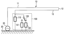
- the antenna device includes a first antenna element 10, a feeding point 20, a ground substrate (GND) 30, and a frequency switching circuit 100.
- the first antenna element 10 is a so-called folded monopole antenna.
- the first antenna element 10 is referred to as the forward path portion 11 from the start point (point connected to the feeding point 20) to the folded portion 12, and is connected from the folded portion 12 to the end point (connected to the GND 30 (grounded)).
- the points up to point) are referred to as the return path section 13.
- the start point of the first antenna element 10 is connected to the feeding point, and the end point is grounded to the GND 30.
- a frequency switching circuit 100 is inserted in the return path unit 13.
- the resonance frequency of the first antenna element 10 can be adjusted by a frequency switching circuit.
- the frequency switching circuit 100 includes a first lumped constant element 110 inserted in the return path section 13 of the first antenna element 10, and a switch 120 and a switch 120 connected in parallel to the first lumped constant element 110.
- a second lumped constant element 131 and a second lumped constant element 132 are connected in series.
- the second lumped constant element 131 and the second lumped constant element 132 may be collectively referred to as a second lumped constant element group.
- the switch 120 is controlled by a control signal (not shown), for example, and selectively connects each of the second lumped constant element groups to the first lumped constant element 110 in parallel.
- the frequency switching circuit 100 corresponds to a parallel connection of the first lumped constant element 110 and the second lumped constant element group selected by the switch 120. Thereby, the frequency switching circuit 100 can adjust the resonance frequency of the first antenna element 10. Further, the frequency switching circuit 100 does not allow the elements to be connected uniformly through the switch, but includes the first lumped constant element 110 inserted into the return path portion of the first antenna element 10 without using the switch 120. Provided. Therefore, the high-frequency current passing through the frequency switching circuit 100 can be dispersed into the current passing through the lumped constant element 110 and the switch 120.
- the frequency switching circuit 100 compared to a configuration in which elements can be connected uniformly through a switch, the high-frequency current passing through the switch is reduced, and the first antenna due to the loss of the active element (switch 120). The influence on the operation of the element 10 can be reduced.
- the antenna device includes the frequency switching circuit 100 in the return path portion 13 of the first antenna element 10 that is a folded monopole antenna.
- the frequency switching circuit 100 includes a first lumped constant element 110 that is directly inserted into the return path portion of the first antenna element 10, a switch 120, and the first lumped constant element 110 via the switch 120. And a second lumped element group that is selectively connected in parallel. Therefore, according to the antenna device according to the present embodiment, the first lumped constant element 110 is directly inserted into the first antenna element 10 without passing through an active element such as the switch 120. Therefore, the first antenna element Compared with the case where both the 10 and the second lumped constant element group can be connected via a switch, the influence of the active element on the operation of the first antenna element 10 can be reduced.
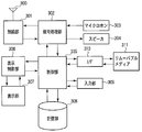
- the antenna device according to each embodiment including the present embodiment can be used for transmission / reception of a radio signal in a communication device (for example, a mobile phone, a PC, etc.) shown in FIG. 21 includes an antenna device 300, a radio unit 301, a signal processing unit 302, a microphone 303, a speaker 304, a control unit 305, a display control unit 306, a display unit 307, a storage unit 308, an input unit 309, and an I / F 310. And a removable medium 311.
- a communication device for example, a mobile phone, a PC, etc.
- FIG. 21 includes an antenna device 300, a radio unit 301, a signal processing unit 302, a microphone 303, a speaker 304, a control unit 305, a display control unit 306, a display unit 307, a storage unit 308, an input unit 309, and an I / F 310.
- a removable medium 311 for example, a mobile phone, a PC, etc.
- the antenna device 300 corresponds to the antenna device according to each embodiment including the present embodiment.
- the antenna device 300 can adjust at least one of the resonance frequencies by switching the state of the internal frequency switching circuit in accordance with, for example, a control signal input from the control unit 305.
- the antenna device of FIG. 21 can obtain the same effect as each embodiment including the present embodiment.
- the radio unit 301 operates in accordance with an instruction from the control unit 305, up-converts a transmission signal output from the signal processing unit 302 to a radio frequency band, and is accommodated in a mobile communication network (not shown) via the antenna device 300. It transmits to a station apparatus, receives the radio signal transmitted from the said base station apparatus via the antenna apparatus 300, and down-converts it to a baseband signal.
- the signal processing unit 302 operates according to an instruction from the control unit 305, converts an audio signal input from the microphone 303 into transmission data, modulates a carrier wave based on the transmission data, and generates the transmission signal.
- the baseband signal input from the wireless unit 301 is demodulated to obtain received data, and an audio signal obtained by decoding the received data is output from the speaker 304.
- the control unit 305 includes a processor such as a CPU, for example, and comprehensively controls each component of the communication apparatus in FIG.
- the storage unit 308 is a storage medium such as a RAM (Random Access Memory), a ROM (Read Only Memory), and a hard disk, and includes a control program and control data of the control unit 305, various data created by the user, and a removable medium 311.
- Control data related to The display control unit 306 drives and controls the display unit 307 in accordance with an instruction from the control unit 305, and causes the display unit 307 to display an image signal based on display data provided from the control unit 305.
- the input unit 309 includes a user interface that receives a request from a user using an input device such as a plurality of key switches (for example, a so-called numeric keypad) or a touch panel.
- the interface (I / F) 310 is an interface for physically and electrically connecting the removable medium 311 to exchange data, and is controlled by the control unit 305.
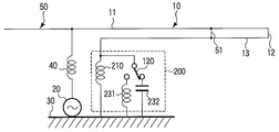
- the antenna device according to the second embodiment of the present invention is configured by replacing the frequency switching circuit 100 with a frequency switching circuit 200 in the antenna device of FIG.
- the frequency switching circuit 200 includes an inductor 210 that is directly inserted into the return path section 13 of the first antenna element 10, and an inductor 231 and a capacitor 232 that can be connected to the inductor 210 in parallel via the switch 120. That is, the frequency switching circuit 200 corresponds to a configuration in which the inductor 210 is employed as the first lumped constant element 110 and the inductor 231 and the capacitor 232 are employed as the second lumped constant element group in the frequency switching circuit 100 described above.
- the inductor 231 is selected by the switch 120 when the resonance frequency is higher than the resonance frequency by the inductor 210 and the antenna element 10, and the capacitor 232 is selected by the switch 120 when the resonance frequency is lower than the resonance frequency by the inductor 210 and the antenna element 10. .
- the lumped constant element employed in the frequency switching circuit 200 may be changed as appropriate according to the frequency characteristics required for the antenna device according to the present embodiment.
- the inductor 210 as the first lumped constant element
- the configuration of the frequency switching circuit shown in FIG. 12A (hereinafter referred to as configuration 1) is compared with the configuration of the frequency switching circuit shown in FIG. 12B (hereinafter referred to as configuration 2).
- Configuration 1 employs an inductor (7.2 nH) as the first lumped constant element
- Configuration 2 employs a capacitor (1.2 pF) as the first lumped constant element
- Configuration 1 employs a capacitor (1.2 pF) as the second lumped constant element
- Configuration 2 employs an inductor (7.2 nH) as the second lumped constant element.
- the configurations 1 and 2 correspond to the parallel connection of the inductor (7.2 nH) and the capacitor (1.2 pF) if the switch is ignored.
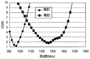
- FIG. 13A shows a simulation result of VSWR when these configurations 1 and 2 are employed
- FIG. 13B shows a simulation result of radiation efficiency. The specific simulation conditions of FIGS.
- the configuration 1 has a lower resonance frequency than the configuration 2. Therefore, if a capacitor and an inductor having the same parameters are used as the first lumped constant element and the second lumped constant element, the configuration 1 in which the inductor is employed as the first lumped constant element has the capacitor as the first lumped constant element. It can be said that a lower resonance frequency can be set as compared with the configuration 2 employed as the constant element.
- the first lumped constant element is an inductor L2 (7.2 nH)
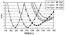
- the second lumped constant element is a capacitor C1 (1.2 pF) and a variable element V1.
- FIG. 16A the simulation result of the radiation efficiency is shown in FIG. 16B.
- the specific simulation conditions in FIGS. 16A and 16B will be described later together with FIGS.
- the resonance frequency becomes higher than when a capacitor is connected, and the change in the resonance frequency due to a change in parameter (inductance) Is small.
- the resonance frequency is lower than when an inductor is connected, and the change in the resonance frequency due to a change in parameter (capacitance) is large.
- the antenna device selects specific elements as the first lumped constant element group and the second lumped constant element group according to desired frequency characteristics. Therefore, according to the antenna device according to the present embodiment, the resonance frequency can be set low by employing, for example, an inductor as the first lumped constant element.
- the antenna device according to the third embodiment of the present invention corresponds to a configuration in which an inductor 40 is directly inserted into the forward path portion 11 of the first antenna element 10 in the antenna device of FIG.
- the antenna device according to the present embodiment may be configured by directly inserting the inductor 40 into the forward path portion 11 of the first antenna element 10 in the antenna devices according to other embodiments.
- the inductor 40 (third lumped constant element) has substantially the same electrical length (that is, inductance) as the element (that is, the inductor 210) that is directly inserted into the return path portion 13 of the first antenna element.
- the inductor 40 is connected to the forward path section 11 so that the electrical length of the forward path section 11 of the first antenna element 10 and the electrical length of the return path section 13 are substantially equal. Inserted directly. Therefore, according to the antenna device according to the present embodiment, since the first antenna element 10 operates in the folded mode, the impedance of the antenna is improved. Therefore, it becomes difficult to receive the influence of the impedance fall by proximity
- the antenna device according to the fourth embodiment of the present invention corresponds to a configuration in which a second antenna element 50 and a stub 51 are further provided in the antenna device of FIG.
- the second antenna element 50 is a monopole antenna that shares a part of the feeding point 20 and the forward path part 11 with the first antenna element 10.
- the second antenna element 50 branches off from the forward path portion 11 of the first antenna element 10.
- the stub 51 short-circuits the forward path portion 11 and the return path portion 13 of the first antenna element.
- the electrical length from the start point of the first antenna element 10 to the end point of the first antenna element 10 via the forward path portion 11, the stub 51 and the return path portion 13 is the resonance of the second antenna element 50. It is desirable that it is 1 ⁇ 2 times the wavelength corresponding to the frequency.
- the frequency characteristics of the antenna device according to the present embodiment will be considered based on simulation. Specifically, it will be demonstrated that the resonance frequency of the first antenna element 10 is switched by the frequency switching circuit 200 and that the resonance frequency of the second antenna element 50 is not easily influenced by the frequency switching circuit 200.
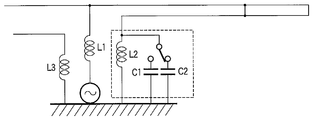
- the antenna apparatus shown in FIG. 8 is a simulation target. The moment method (4 NEC2) is used for the simulation. In the antenna device of FIG. 8, a parasitic antenna element is shown. This antenna element will be described in the sixth embodiment. In the antenna apparatus of FIG. 8, the parameters are as follows.
- Inductor L1 has an inductance of 7.2 nH
- inductor L2 has an inductance of 7.2 nH
- inductor L3 has an inductance of 0 nH
- capacitor C1 has a capacitance of 1.2 pF
- capacitor C2 has a capacitance of 0.5 pF. It is.
- the switch is expressed by an equivalent circuit model of the MESFET switch. Specifically, assume that the switch insertion loss is 0.25 dB and the isolation is about 32 dB. At this time, in the 50 ⁇ system, the switch is equivalent to a 3 ⁇ resistor in the ON state, and is equivalent to a parallel connection of a 3500 ⁇ resistor and a 0.5 pF capacitor in the OFF state.
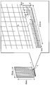
- FIG. 8 is represented by the simulation model shown in FIG. FIG. 9 shows specific dimensions of the antenna element and the ground substrate.
- the dotted line portion represents the frequency switching circuit.
- state1 a state in which the capacitor C1 is selected via the switch
- state2 a state in which the capacitor C2 is selected via the switch
- FIG. 10A shows the VSWR of the antenna device of FIG. 8 in the vicinity of the resonance frequency of the first antenna element.
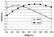
- FIG. 11A shows the radiation characteristics of the antenna device of FIG. 8 near the resonance frequency of the first antenna element.
- the resonance frequency of the first antenna element changes according to the state of the frequency switching circuit.
- FIG. 10B represents the VSWR of the antenna device of FIG. 8 near the resonance frequency of the second antenna element.
- FIG. 11B represents the radiation characteristic of the antenna device of FIG. 8 near the resonance frequency of the second antenna element.
- the resonance frequency of the second antenna element is constant regardless of the state of the frequency switching circuit.
- FIG. 22A represents the radiation characteristic of the antenna device in the vicinity of the resonance frequency of the first antenna element.
- FIG. 22B represents the radiation characteristics of the antenna device in the vicinity of the resonance frequency of the second antenna element.
- the resonance frequency of the second antenna element is constant regardless of the state of the frequency switching circuit.
- the resonant frequency which can be read from FIG. 22A and FIG. 22B has fallen, this is considered to be the influence of the dielectric material used for mounting of an antenna apparatus.
- the electrical length from the start point of the first antenna element to the end point of the first antenna element via the forward path, the stub, and the return path is the resonance frequency of the second antenna element. It is desirable to provide a stub so as to be 1/2 the corresponding wavelength. If the stub is offset from this position, the resonance frequency of the second antenna element is affected by the frequency switching circuit.
- FIG. 14A shows the VSWR (in the vicinity of the resonance frequency of the second antenna element) when the stub position is offset by ⁇ 10 mm (10 mm in the direction opposite to the folded portion) in the antenna device of FIG. FIG.
- FIGS. 14A and 14B shows VSWR (in the vicinity of the resonance frequency of the second antenna element) when the stub position is offset by +5 mm (5 mm in the direction of the folded portion) in the antenna device of FIG.
- the second antenna element is affected by the frequency switching circuit depending on the position of the stub, so that attention is required.
- the antenna device short-circuits the second antenna element branched from the forward path portion of the first antenna element and the forward path portion and the return path portion of the first antenna element.
- a stub is provided. Therefore, according to the antenna device according to the present embodiment, it is possible to add a resonance mode that is not affected by the frequency switching circuit.
- the antenna device according to the fifth embodiment of the present invention corresponds to a configuration in which a third antenna element 60 is further provided in the antenna device of FIG.
- the antenna device according to this embodiment may be configured by additionally providing a third antenna element 60 in the antenna devices according to other embodiments.
- the third antenna element 60 branches from the return path portion 13 of the first antenna element 10 and includes a contact point to the switch 120.
- the resonance frequency of the third antenna element 60 changes according to the state of the frequency switching circuit 200.
- the frequency characteristics of the antenna device according to the present embodiment will be considered based on simulation. Specifically, it will be demonstrated that the resonance frequency of the first antenna element 10 is switched by the frequency switching circuit 200, the resonance frequency of the third antenna element 60 is also switched by the frequency switching circuit 200, and the like.
- the antenna device shown in FIG. 17 is a simulation target. The moment method (4 NEC2) is used for the simulation. In the antenna device of FIG. 17, the parameters are as follows.
- the inductance of the inductor L1 is 7.2 nH
- the inductance of the inductor L2 is 7.2 nH
- the capacitance of the capacitor C1 is 0.2 pF
- the capacitance of the capacitor C2 is 0.5 pF.
- the switch is expressed by an equivalent circuit model of the MESFET switch. Specifically, assume that the switch insertion loss is 0.25 dB and the isolation is about 32 dB. At this time, in the 50 ⁇ system, the switch is equivalent to a 3 ⁇ resistor in the ON state, and is equivalent to a parallel connection of a 3500 ⁇ resistor and a 0.5 pF capacitor in the OFF state.
- the antenna of FIG. 17 is represented by a simulation model shown in FIG. FIG. 18 shows specific dimensions of the antenna element and the ground substrate. In FIG. 18, the dotted line portion represents the frequency switching circuit.
- a state in which the capacitor C1 is selected through the switch is referred to as state 1
- a state in which the capacitor C2 is selected through the switch is referred to as state 2.
- FIG. 19A shows the VSWR of the antenna device of FIG. 17 in the vicinity of the resonance frequency of the first antenna element.
- FIG. 20A represents the radiation characteristic of the antenna device of FIG. 17 near the resonance frequency of the first antenna element.
- the resonance frequency of the first antenna element changes in accordance with the state of the frequency switching circuit.
- FIG. 19B represents the VSWR of the antenna of FIG. 17 near the resonance frequency of the third antenna element.
- FIG. 20B shows the radiation characteristic of the antenna device of FIG. 17 near the resonance frequency of the third antenna element.
- the resonance frequency of the third antenna element also changes according to the state of the frequency switching circuit.
- the antenna device includes the third antenna element that branches from the return path portion of the first antenna element and includes a contact point to the switch. Therefore, according to the antenna device according to the present embodiment, it is possible to add a resonance mode capable of changing the frequency according to the state of the frequency switching circuit.
- the antenna device according to the sixth embodiment of the present invention corresponds to a configuration in which a fourth antenna element 70 and an inductor 71 are further provided in the antenna device of FIG.
- the antenna device according to the present embodiment may be configured by additionally providing a fourth antenna element 70 and an inductor 71 in the antenna devices according to other embodiments.
- the fourth antenna element 70 is a parasitic element.
- the fourth antenna element 70 is grounded to the GND 30 at a position close to the feeding point 20.
- the fourth antenna element 70 is not affected by the frequency switching circuit 200.
- the antenna device includes the fourth antenna element that is not fed. Therefore, according to the antenna device according to the present embodiment, it is possible to add a resonance mode that is not affected by the frequency switching circuit.
- the antenna device according to the seventh embodiment of the present invention corresponds to a configuration in which a control signal source 90 and a low-pass filter 91 are further provided in the antenna device of FIG.
- the antenna device according to this embodiment may be configured by additionally providing a control signal source 90 and a low-pass filter 91 in the antenna devices according to other embodiments.
- the control signal source 90 generates a control signal given to the switch 120.
- the low-pass filter 91 performs a filtering process to suppress the high-frequency component of the control signal from the control signal source 90 and gives the low-frequency component of the control signal to the switch 120.
- the low-pass filter 91 performs the same filtering process on the power supply signal.
- it is desirable that the cutoff frequency of the low-pass filter 91 is lower than all the operating frequencies supported by the antenna device according to the present embodiment.
- the antenna device according to the present embodiment performs low-pass filter processing on the control signal given to the switch 120. Therefore, according to the antenna device according to the present embodiment, it is possible to suppress degradation of antenna characteristics due to the high-frequency current of the antenna device being coupled to the control signal line.
- the present invention is not limited to the above-described embodiments as they are, and can be embodied by modifying the constituent elements without departing from the scope of the invention in the implementation stage.
- Various inventions can be formed by appropriately combining a plurality of constituent elements disclosed in the above embodiments. Further, for example, a configuration in which some components are deleted from all the components shown in each embodiment is also conceivable. Furthermore, you may combine suitably the component described in different embodiment.
- Antenna device 301 ... Radio unit 302 ... Signal processing unit 303 ... Microphone 304 ... Speaker 305 ... Control unit 306 ... Display control unit 307 ... Display unit 308 ... Storage unit 309 ... Input unit 310 ... I / F 311 ... Removable media
Landscapes
- Engineering & Computer Science (AREA)
- Computer Networks & Wireless Communication (AREA)
- Signal Processing (AREA)
- Variable-Direction Aerials And Aerial Arrays (AREA)
- Details Of Aerials (AREA)
- Transceivers (AREA)
Abstract
アンテナ装置は、始点が給電点(20)に接続された往路部(11)と、折り返し部(12)と、終点が接地された復路部(13)とを含む第1のアンテナ素子(10)と、復路部(13)に挿入される第1の集中定数素子(110)と、制御信号に従って経路選択をするスイッチ(120)と、スイッチ(120)を介して第1の集中定数素子(110)に対して選択的に並列接続される第2の集中定数素子(131,132)とを具備する。
Description
本発明は、周波数チューナブル技術に関する。
携帯端末(例えば、携帯電話機)、PCなどに実装されるアンテナには、小型化が要求される。また、アンテナは複数の無線通信システムへの対応のために広帯域をサポートすることも要求される。
特許文献1記載のアンテナ装置は、多共振アンテナを用いて複数の無線通信システムをサポートしている。具体的には、このアンテナ装置は、折り返しモノポールアンテナに給電点を共有する別のアンテナ素子を付加することにより多共振アンテナを形成している。
特許文献2記載のアンテナ装置は、インピーダンス調整手段によってアンテナ装置の動作周波数を調整している。具体的には、このアンテナ装置は、アンテナ素子の開放端のインピーダンスを調整することにより動作周波数を調整する。このアンテナ装置は、動作周波数の調整によって広帯域をサポートする。
特許文献1記載のアンテナ装置を小型化すると、多共振アンテナの各素子でサポート可能な帯域が減少し、結果として一部帯域の確保が困難となる問題がある。また、周波数チューナブルアンテナ(リコンフィギュアラブルアンテナ)に関して、特許文献2記載のアンテナ装置のように、スイッチなどのアクティブ素子を用いてアンテナ装置に接続する素子を切り替えてアンテナの動作周波数を調整する構成が知られている。しかしながら、アクティブ素子の損失がアンテナ放射効率に影響を与える。更に、この影響はアンテナ装置の小型化に伴って、アンテナ素子の放射抵抗の減少によって顕著に現れる。また、アンテナ装置を多共振アンテナで構成し、周波数チューナブル技術を適用する場合に、調整の必要な共振周波数と調整の不要な共振周波数とが混在する可能性がある。また、携帯端末、PCに実装されるアンテナ装置では、実装性の観点から、給電点は1つに共通化されることが望ましい。
従って、本発明はアクティブ素子の損失によるアンテナ素子への影響を低減可能な周波数チューナブル技術を提供することを目的とする。
本発明の一態様に係るアンテナ装置は、始点が給電点に接続された往路部と、折り返し部と、終点が接地された復路部とを含む第1のアンテナ素子と、前記復路部に挿入される第1の集中定数素子と、制御信号に従って経路選択をするスイッチと、前記スイッチを介して前記第1の集中定数素子に対して選択的に並列接続される第2の集中定数素子とを具備する。
本発明の他の態様に係る通信装置は、始点が給電点に接続された往路部と、折り返し部と、終点が接地された復路部とを含む第1のアンテナ素子と、前記復路部に挿入される第1の集中定数素子と、制御信号に従って経路選択をするスイッチと、前記スイッチを介して前記第1の集中定数素子に対して選択的に並列接続される第2の集中定数素子とを含むアンテナ装置と、ベースバンドの送信信号を前記アンテナ装置から送信される無線送信信号にアップコンバートし、前記アンテナ装置から受信された無線受信信号をベースバンドの受信信号にダウンコンバートする無線部と、前記送信信号及び前記受信信号に対して信号処理を行う信号処理部とを具備する。
本発明によれば、アクティブ素子の損失によるアンテナ素子への影響を低減可能な周波数チューナブル技術を提供できる。
以下、図面を参照して、本発明の実施形態について説明する。
(第1の実施形態)
図1に示すように、本発明の第1の実施形態に係るアンテナ装置は、第1のアンテナ素子10、給電点20、グラウンド基板(GND)30及び周波数切り替え回路100を有する。
(第1の実施形態)
図1に示すように、本発明の第1の実施形態に係るアンテナ装置は、第1のアンテナ素子10、給電点20、グラウンド基板(GND)30及び周波数切り替え回路100を有する。
第1のアンテナ素子10は、いわゆる折り返しモノポールアンテナである。以降の説明において、第1のアンテナ素子10に関して、始点(給電点20に接続される点)から折り返し部12までを往路部11と称し、折り返し部12から終点(GND30に接続(接地)される点)までを復路部13と称する。第1のアンテナ素子10の始点は給電点に接続され、終点はGND30に接地される。復路部13には、周波数切り替え回路100が挿入されている。第1のアンテナ素子10の共振周波数は、周波数切り替え回路によって調整できる。
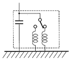
周波数切り替え回路100は、第1のアンテナ素子10の復路部13に挿入される第1の集中定数素子110と、この第1の集中定数素子110に対して並列接続されるスイッチ120とスイッチ120に対して直列接続される第2の集中定数素子131及び第2の集中定数素子132を含む。尚、以降の説明において、第2の集中定数素子131及び第2の集中定数素子132を第2の集中定数素子群として総称することもある。スイッチ120は、例えば図示しない制御信号によって制御され、第2の集中定数素子群の各々を第1の集中定数素子110に対して選択的に並列接続させる。即ち、周波数切り替え回路100は、第1の集中定数素子110と、第2の集中定数素子群のうちスイッチ120によって選択されたものとの並列接続に相当する。これによって、周波数切り替え回路100は、第1のアンテナ素子10の共振周波数を調整できる。また、周波数切り替え回路100は、一律にスイッチを介して素子を接続可能とするのでなく、スイッチ120を介さずに第1のアンテナ素子10の復路部に挿入される第1の集中定数素子110を設けている。従って、周波数切り替え回路100を通過する高周波電流を集中定数素子110とスイッチ120を通過する電流に分散できる。故に、周波数切り替え回路100によれば、一律にスイッチを介して素子を接続可能とする構成に比べて、スイッチを通過する高周波電流を低減し、アクティブ素子(スイッチ120)の損失による第1のアンテナ素子10の動作への影響を低減できる。
以上説明したように、本実施形態に係るアンテナ装置は、折り返しモノポールアンテナである第1のアンテナ素子10の復路部13に周波数切り替え回路100を設けている。そして、この周波数切り替え回路100は、第1のアンテナ素子10の復路部に直接挿入される第1の集中定数素子110と、スイッチ120と、このスイッチ120を介して第1の集中定数素子110と選択的に並列接続される第2の集中定数素子群とを含む。従って、本実施形態に係るアンテナ装置によれば、第1の集中定数素子110がスイッチ120のようなアクティブ素子を介さずに第1のアンテナ素子10に直接挿入されるため、第1のアンテナ素子10及び第2の集中定数素子群の両方をスイッチを介して接続可能とする場合に比べてアクティブ素子による第1のアンテナ素子10の動作への影響を低減できる。
また、本実施形態を含む各実施形態に係るアンテナ装置は、例えば図21に示すような通信装置(例えば、携帯電話機、PCなど)において無線信号の送受信のために使用可能である。図21の通信装置は、アンテナ装置300、無線部301、信号処理部302、マイクロホン303、スピーカ304、制御部305、表示制御部306、表示部307、記憶部308、入力部309、I/F310、リムーバブルメディア311を有する。
アンテナ装置300は、本実施形態を含む各実施形態に係るアンテナ装置に相当する。アンテナ装置300は、例えば制御部305から入力される制御信号に従って内部の周波数切り替え回路の状態を切り替えることによって、共振周波数の少なくとも1つを調整可能である。アンテナ装置300として、本実施形態を含む各実施形態に係るアンテナ装置を使用することにより、図21のアンテナ装置は本実施形態を含む各実施形態と同じ効果を得ることができる。
無線部301は、制御部305からの指示に従って動作し、信号処理部302から出力される送信信号を無線周波数帯にアップコンバートし、アンテナ装置300を介して図示しない移動通信網に収容される基地局装置に送信したり、上記基地局装置から送信された無線信号をアンテナ装置300を介して受信してベースバンド信号にダウンコンバートしたりする。
信号処理部302は、制御部305からの指示に従って動作し、マイクロホン303から入力された音声信号を送信データに変換し、当該送信データに基づいて搬送波を変調して上記送信信号を生成したり、無線部301から入力される上記ベースバンド信号を復調して受信データを得て、当該受信データを復号して得た音声信号をスピーカ304より出力したりする。制御部305は、例えばCPUなどのプロセッサを備え、図21の通信装置の各構成要素を統括制御する。
記憶部308には、RAM(Random Access Memory)やROM(Read Only Memory)、ハードディスクなどの記憶媒体であって、制御部305の制御プログラムや制御データ、ユーザが作成した種々のデータ、リムーバブルメディア311に関わる制御データなどを記憶する。表示制御部306は、制御部305からの指示に従って、表示部307を駆動制御し、制御部305から与えられる表示データに基づく画像信号を表示部307に表示させる。入力部309は、複数のキースイッチ(例えば、いわゆるテンキー(numeric keypad))やタッチパネルなどの入力デバイスを用いて、ユーザからの要求を受理するユーザインタフェースを含む。インタフェース(I/F)310は、リムーバブルメディア311を物理的及び電気的に接続して、データ交換を行うためのインタフェースであって、制御部305によって制御される。
(第2の実施形態)
図2に示すように、本発明の第2の実施形態に係るアンテナ装置は、図1のアンテナ装置において周波数切り替え回路100を周波数切り替え回路200に置き換えて構成している。以下の説明では、図2において図1と同一部分には同一符号を付して示し、異なる部分を中心に述べる。
図2に示すように、本発明の第2の実施形態に係るアンテナ装置は、図1のアンテナ装置において周波数切り替え回路100を周波数切り替え回路200に置き換えて構成している。以下の説明では、図2において図1と同一部分には同一符号を付して示し、異なる部分を中心に述べる。
周波数切り替え回路200は、第1のアンテナ素子10の復路部13に直接挿入されるインダクタ210と、このインダクタ210に対してスイッチ120を介して並列接続可能なインダクタ231及びキャパシタ232を含む。即ち、周波数切り替え回路200は、前述した周波数切り替え回路100において第1の集中定数素子110としてインダクタ210を採用し、第2の集中定数素子群としてインダクタ231及びキャパシタ232を採用した構成に相当する。共振周波数をインダクタ210とアンテナ素子10による共振周波数より高くするときにはインダクタ231がスイッチ120によって選択され、共振周波数をインダクタ210とアンテナ素子10による共振周波数より低くするときにはキャパシタ232がスイッチ120によって選択される。尚、周波数切り替え回路200において採用される集中定数素子は、本実施形態に係るアンテナ装置に要求される周波数特性に応じて適宜変更されてよい。
以下、第1の集中定数素子としてインダクタ210を採用することの技術的意義を説明する。
一般に、アンテナ装置を小型化するほど、共振周波数を低くすることが困難となる。故に、本実施形態に係るアンテナ装置を小型に構成する場合を想定すると、周波数切り替え回路200はより低い共振周波数を設定可能であることが望ましいと考えられる。そこで、第1の集中定数素子としてインダクタを採用する場合と、キャパシタを採用する場合とでアンテナ素子10の周波数特性にどのような差異が生じるかを検討する。具体的には、図12Aに示す周波数切り替え回路の構成(以下、構成1と称する)と、図12Bに示す周波数切り替え回路の構成(以下、構成2と称する)とを比較する。構成1は第1の集中定数素子としてインダクタ(7.2nH)を採用し、構成2は第1の集中定数素子としてキャパシタ(1.2pF)を採用している。一方、構成1は第2の集中定数素子としてキャパシタ(1.2pF)を採用し、構成2は第2の集中定数素子としてインダクタ(7.2nH)を採用している。即ち、構成1及び構成2は、スイッチを無視すれば、いずれもインダクタ(7.2nH)及びキャパシタ(1.2pF)の並列接続に相当する。これら構成1及び構成2を夫々採用した場合におけるVSWRのシミュレーション結果を図13Aに示し、放射効率のシミュレーション結果を図13Bに示す。尚、図13A及び図13Bの具体的なシミュレーション条件は、図8及び図9と共に後述する。図13A及び図13Bから明らかなように、構成1は構成2に比べて共振周波数が低い。故に、同一パラメータのキャパシタ及びインダクタを第1の集中定数素子及び第2の集中定数素子として使用するのであれば、インダクタを第1の集中定数素子として採用する構成1が、キャパシタを第1の集中定数素子として採用する構成2に比べて低い共振周波数を設定可能であるといえる。
一般に、アンテナ装置を小型化するほど、共振周波数を低くすることが困難となる。故に、本実施形態に係るアンテナ装置を小型に構成する場合を想定すると、周波数切り替え回路200はより低い共振周波数を設定可能であることが望ましいと考えられる。そこで、第1の集中定数素子としてインダクタを採用する場合と、キャパシタを採用する場合とでアンテナ素子10の周波数特性にどのような差異が生じるかを検討する。具体的には、図12Aに示す周波数切り替え回路の構成(以下、構成1と称する)と、図12Bに示す周波数切り替え回路の構成(以下、構成2と称する)とを比較する。構成1は第1の集中定数素子としてインダクタ(7.2nH)を採用し、構成2は第1の集中定数素子としてキャパシタ(1.2pF)を採用している。一方、構成1は第2の集中定数素子としてキャパシタ(1.2pF)を採用し、構成2は第2の集中定数素子としてインダクタ(7.2nH)を採用している。即ち、構成1及び構成2は、スイッチを無視すれば、いずれもインダクタ(7.2nH)及びキャパシタ(1.2pF)の並列接続に相当する。これら構成1及び構成2を夫々採用した場合におけるVSWRのシミュレーション結果を図13Aに示し、放射効率のシミュレーション結果を図13Bに示す。尚、図13A及び図13Bの具体的なシミュレーション条件は、図8及び図9と共に後述する。図13A及び図13Bから明らかなように、構成1は構成2に比べて共振周波数が低い。故に、同一パラメータのキャパシタ及びインダクタを第1の集中定数素子及び第2の集中定数素子として使用するのであれば、インダクタを第1の集中定数素子として採用する構成1が、キャパシタを第1の集中定数素子として採用する構成2に比べて低い共振周波数を設定可能であるといえる。
以下、第2の集中定数素子群としてどのような集中定数素子を接続すべきかについて考察する。
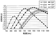
まず、図15に示すような周波数切り替え回路の構成を想定する。図15の周波数切り替え回路において、第1の集中定数素子はインダクタL2(7.2nH)であり、第2の集中定数素子はキャパシタC1(1.2pF)及び可変素子V1である。可変素子V1をスイッチによって選択し、この可変素子V1のパラメータを1.2nH、4.2nH、7.2nH、0.2pF、1.2pF及び2.2pFに夫々変化させた場合におけるVSWRのシミュレーション結果を図16Aに示し、放射効率のシミュレーション結果を図16Bに示す。尚、図16A及び図16Bの具体的なシミュレーション条件は、図8及び図9と共に後述する。図16A及び図16Bから明らかなように、第2の集中定数素子としてインダクタを接続すると、キャパシタを接続する場合に比べて共振周波数は高くなり、また、パラメータ(インダクタンス)の変化による共振周波数の変化が小さい。一方、第2の集中定数素子としてキャパシタを接続すると、インダクタを接続する場合に比べて共振周波数は低くなり、また、パラメータ(キャパシタンス)の変化による共振周波数の変化が大きい。
まず、図15に示すような周波数切り替え回路の構成を想定する。図15の周波数切り替え回路において、第1の集中定数素子はインダクタL2(7.2nH)であり、第2の集中定数素子はキャパシタC1(1.2pF)及び可変素子V1である。可変素子V1をスイッチによって選択し、この可変素子V1のパラメータを1.2nH、4.2nH、7.2nH、0.2pF、1.2pF及び2.2pFに夫々変化させた場合におけるVSWRのシミュレーション結果を図16Aに示し、放射効率のシミュレーション結果を図16Bに示す。尚、図16A及び図16Bの具体的なシミュレーション条件は、図8及び図9と共に後述する。図16A及び図16Bから明らかなように、第2の集中定数素子としてインダクタを接続すると、キャパシタを接続する場合に比べて共振周波数は高くなり、また、パラメータ(インダクタンス)の変化による共振周波数の変化が小さい。一方、第2の集中定数素子としてキャパシタを接続すると、インダクタを接続する場合に比べて共振周波数は低くなり、また、パラメータ(キャパシタンス)の変化による共振周波数の変化が大きい。
以上説明したように、本実施形態に係るアンテナ装置は、所望の周波数特性に応じて第1の集中定数素子及び第2の集中定数素子群として具体的な素子を選択している。従って、本実施形態に係るアンテナ装置によれば、例えば第1の集中定数素子としてインダクタを採用することによって、共振周波数を低く設定できる。
(第3の実施形態)
図3に示すように、本発明の第3の実施形態に係るアンテナ装置は、図2のアンテナ装置において第1のアンテナ素子10の往路部11にインダクタ40を直接挿入した構成に相当する。以下の説明では、図3において図2と同一部分には同一符号を付して示し、異なる部分を中心に述べる。尚、本実施形態に係るアンテナ装置は、その他の実施形態に係るアンテナ装置において第1のアンテナ素子10の往路部11にインダクタ40を直接挿入することにより構成されてもよい。
図3に示すように、本発明の第3の実施形態に係るアンテナ装置は、図2のアンテナ装置において第1のアンテナ素子10の往路部11にインダクタ40を直接挿入した構成に相当する。以下の説明では、図3において図2と同一部分には同一符号を付して示し、異なる部分を中心に述べる。尚、本実施形態に係るアンテナ装置は、その他の実施形態に係るアンテナ装置において第1のアンテナ素子10の往路部11にインダクタ40を直接挿入することにより構成されてもよい。
インダクタ40(第3の集中定数素子)は、第1のアンテナ素子の復路部13に直接挿入される素子(即ち、インダクタ210)と電気長(即ち、インダクタンス)が略等しい。
以上説明したように、本実施形態に係るアンテナ装置は、第1のアンテナ素子10の往路部11の電気長と復路部13の電気長とが略等しくなるように、インダクタ40を往路部11に直接挿入している。従って、本実施形態に係るアンテナ装置によれば、第1のアンテナ素子10が折り返しモードで動作するため、アンテナのインピーダンスが向上する。従って、GND30などの周辺金属の近接によるインピーダンス低下の影響を受けにくくなる。
(第4の実施形態)
図4に示すように、本発明の第4の実施形態に係るアンテナ装置は、図3のアンテナ装置において第2のアンテナ素子50及びスタブ51を更に設けた構成に相当する。以下の説明では、図4において図3と同一部分には同一符号を付して示し、異なる部分を中心に述べる。尚、本実施形態に係るアンテナ装置は、その他の実施形態に係るアンテナ装置において第2のアンテナ素子50及びスタブ51を付加的に設けることにより構成されてもよい。
図4に示すように、本発明の第4の実施形態に係るアンテナ装置は、図3のアンテナ装置において第2のアンテナ素子50及びスタブ51を更に設けた構成に相当する。以下の説明では、図4において図3と同一部分には同一符号を付して示し、異なる部分を中心に述べる。尚、本実施形態に係るアンテナ装置は、その他の実施形態に係るアンテナ装置において第2のアンテナ素子50及びスタブ51を付加的に設けることにより構成されてもよい。
第2のアンテナ素子50は、給電点20と往路部11の一部を第1のアンテナ素子10と共有するモノポールアンテナである。第2のアンテナ素子50は、第1のアンテナ素子10の往路部11から分岐している。スタブ51は、第1のアンテナ素子の往路部11と復路部13との間を短絡している。尚、第1のアンテナ素子10の始点から往路部11とスタブ51と復路部13とを経由して第1のアンテナ素子10の終点に至るまでの電気長は、第2のアンテナ素子50の共振周波数に対応する波長の1/2倍であることが望ましい。このようなスタブ51を設けることにより、第2のアンテナ素子50の共振周波数への周波数切り替え回路200による影響を低減できる。即ち、第1のアンテナ素子10の共振周波数が切り替えられたとしても、第2のアンテナ素子50の共振周波数は変化しにくくなる。
以下、シミュレーションに基づいて本実施形態に係るアンテナ装置の周波数特性を考察する。具体的には、第1のアンテナ素子10の共振周波数は周波数切り替え回路200によって切り替えられること、第2のアンテナ素子50の共振周波数は周波数切り替え回路200の影響を受けにくいことなどを実証する。
図8に示すアンテナ装置がシミュレーションの対象となる。シミュレーションにはモーメント法(4NEC2)を用いる。尚、図8のアンテナ装置において、無給電のアンテナ素子が示されているが、このアンテナ素子については第6の実施形態において説明する。図8のアンテナ装置において、パラメータは次の通りである。インダクタL1のインダクタンスは7.2nHであり、インダクタL2のインダクタンスは7.2nHであり、インダクタL3のインダクタンスは0nHであり、キャパシタC1のキャパシタンスは1.2pFであり、キャパシタC2のキャパシタンスは0.5pFである。また、スイッチは、MESFETスイッチの等価回路モデルで表現する。具体的には、スイッチの挿入損失は0.25dBであって、アイソレーションは約32dBであると仮定する。このとき、スイッチは50Ω系ではON状態において3Ωの抵抗と等価であり、OFF状態において3500Ωの抵抗と0.5pFのキャパシタの並列接続と等価である。図8のアンテナは、図9に示すシミュレーションモデルで表される。図9は、アンテナ素子、グラウンド基板の具体的寸法を示している。尚、図9において点線部分は周波数切り替え回路を表している。以降の説明において、図8のアンテナ装置に関して、スイッチを介してキャパシタC1を選択した状態をstate1と称し、スイッチを介してキャパシタC2を選択した状態をstate2と称する。
図8に示すアンテナ装置がシミュレーションの対象となる。シミュレーションにはモーメント法(4NEC2)を用いる。尚、図8のアンテナ装置において、無給電のアンテナ素子が示されているが、このアンテナ素子については第6の実施形態において説明する。図8のアンテナ装置において、パラメータは次の通りである。インダクタL1のインダクタンスは7.2nHであり、インダクタL2のインダクタンスは7.2nHであり、インダクタL3のインダクタンスは0nHであり、キャパシタC1のキャパシタンスは1.2pFであり、キャパシタC2のキャパシタンスは0.5pFである。また、スイッチは、MESFETスイッチの等価回路モデルで表現する。具体的には、スイッチの挿入損失は0.25dBであって、アイソレーションは約32dBであると仮定する。このとき、スイッチは50Ω系ではON状態において3Ωの抵抗と等価であり、OFF状態において3500Ωの抵抗と0.5pFのキャパシタの並列接続と等価である。図8のアンテナは、図9に示すシミュレーションモデルで表される。図9は、アンテナ素子、グラウンド基板の具体的寸法を示している。尚、図9において点線部分は周波数切り替え回路を表している。以降の説明において、図8のアンテナ装置に関して、スイッチを介してキャパシタC1を選択した状態をstate1と称し、スイッチを介してキャパシタC2を選択した状態をstate2と称する。
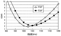
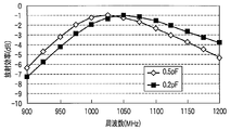
図10Aは、第1のアンテナ素子の共振周波数付近における図8のアンテナ装置のVSWRを表している。図11Aは、第1のアンテナ素子の共振周波数付近における図8のアンテナ装置の放射特性を表している。図10A及び図11Aから明らかなように、第1のアンテナ素子の共振周波数は、周波数切り替え回路の状態に応じて変化している。一方、図10Bは、第2のアンテナ素子の共振周波数付近における図8のアンテナ装置のVSWRを表している。図11Bは、第2のアンテナ素子の共振周波数付近における図8のアンテナ装置の放射特性を表している。図10B及び図11Bから明らかなように、第2のアンテナ素子の共振周波数は、周波数切り替え回路の状態に関わらず一定である。
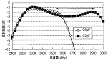
更に、図8のアンテナ装置を実装し、放射特性を確認したところ、図11A及び図11Bのシミュレーション結果に対応する実験結果を得ることができた。図22Aは、第1のアンテナ素子の共振周波数付近におけるアンテナ装置の放射特性を表している。図22Aから明らかなように、第1のアンテナ素子の共振周波数は、周波数切り替え回路の状態に応じて変化している。一方、図22Bは、第2のアンテナ素子の共振周波数付近におけるアンテナ装置の放射特性を表している。図22Bから明らかなように、第2のアンテナ素子の共振周波数は、周波数切り替え回路の状態に関わらず一定である。尚、図11A及び図11Bに比べて、図22A及び図22Bから読みとれる共振周波数は低下しているが、これはアンテナ装置の実装に用いた誘電体の影響であると考えられる。
ところで、前述のように、第1のアンテナ素子の始点から往路部とスタブと復路部とを経由して第1のアンテナ素子の終点に至るまでの電気長が第2のアンテナ素子の共振周波数に対応する波長の1/2倍となるように、スタブを設けることが望ましい。スタブをこの位置からをオフセットさせると、第2のアンテナ素子の共振周波数が周波数切り替え回路の影響を受けてしまう。例えば、図14Aは、図8のアンテナ装置においてスタブ位置を-10mm(折り返し部と反対方向に10mm)オフセットさせた場合の(第2のアンテナ素子の共振周波数付近の)VSWRを表している。また、図14Bは、図8のアンテナ装置においてスタブ位置を+5mm(折り返し部の方向に5mm)オフセットさせた場合の(第2のアンテナ素子の共振周波数付近の)VSWRを表している。図14A及び図14Bから明らかなように、スタブの位置によっては第2のアンテナ素子が周波数切り替え回路の影響を受けてしまうため注意を要する。
以上説明したように、本実施形態に係るアンテナ装置は、第1のアンテナ素子の往路部から分岐する第2のアンテナ素子と、第1のアンテナ素子の往路部と復路部との間を短絡するスタブとを設けている。従って、本実施形態に係るアンテナ装置によれば、周波数切り替え回路の影響を受けない共振モードを追加できる。
(第5の実施形態)
図5に示すように、本発明の第5の実施形態に係るアンテナ装置は、図4のアンテナ装置において、第3のアンテナ素子60を更に設けた構成に相当する。以下の説明では、図5において図4と同一部分には同一符号を付して示し、異なる部分を中心に述べる。尚、本実施形態に係るアンテナ装置は、その他の実施形態に係るアンテナ装置において第3のアンテナ素子60を付加的に設けることにより構成されてもよい。
図5に示すように、本発明の第5の実施形態に係るアンテナ装置は、図4のアンテナ装置において、第3のアンテナ素子60を更に設けた構成に相当する。以下の説明では、図5において図4と同一部分には同一符号を付して示し、異なる部分を中心に述べる。尚、本実施形態に係るアンテナ装置は、その他の実施形態に係るアンテナ装置において第3のアンテナ素子60を付加的に設けることにより構成されてもよい。
第3のアンテナ素子60は、第1のアンテナ素子10の復路部13から分岐し、スイッチ120への接点を含んでいる。この第3のアンテナ素子60の共振周波数は、周波数切り替え回路200の状態に応じて変化する。
以下、シミュレーションに基づいて本実施形態に係るアンテナ装置の周波数特性を考察する。具体的には、第1のアンテナ素子10の共振周波数は周波数切り替え回路200によって切り替えられること、第3のアンテナ素子60の共振周波数もまた周波数切り替え回路200によって切り替えられることなどを実証する。
図17に示すアンテナ装置がシミュレーションの対象となる。シミュレーションにはモーメント法(4NEC2)を用いる。図17のアンテナ装置において、パラメータは次の通りである。インダクタL1のインダクタンスは7.2nHであり、インダクタL2のインダクタンスは7.2nHであり、キャパシタC1のキャパシタンスは0.2pFであり、キャパシタC2のキャパシタンスは0.5pFである。また、スイッチは、MESFETスイッチの等価回路モデルで表現する。具体的には、スイッチの挿入損失は0.25dBであって、アイソレーションは約32dBであると仮定する。このとき、スイッチは50Ω系ではON状態において3Ωの抵抗と等価であり、OFF状態において3500Ωの抵抗と0.5pFのキャパシタの並列接続と等価である。図17のアンテナは、図18に示すシミュレーションモデルで表される。図18は、アンテナ素子、グラウンド基板の具体的寸法を示している。尚、図18において点線部分は周波数切り替え回路を表している。以降の説明において、図17のアンテナ装置に関して、スイッチを介してキャパシタC1を選択した状態をstate1とし、スイッチを介してキャパシタC2を選択した状態をstate2と称する。
図17に示すアンテナ装置がシミュレーションの対象となる。シミュレーションにはモーメント法(4NEC2)を用いる。図17のアンテナ装置において、パラメータは次の通りである。インダクタL1のインダクタンスは7.2nHであり、インダクタL2のインダクタンスは7.2nHであり、キャパシタC1のキャパシタンスは0.2pFであり、キャパシタC2のキャパシタンスは0.5pFである。また、スイッチは、MESFETスイッチの等価回路モデルで表現する。具体的には、スイッチの挿入損失は0.25dBであって、アイソレーションは約32dBであると仮定する。このとき、スイッチは50Ω系ではON状態において3Ωの抵抗と等価であり、OFF状態において3500Ωの抵抗と0.5pFのキャパシタの並列接続と等価である。図17のアンテナは、図18に示すシミュレーションモデルで表される。図18は、アンテナ素子、グラウンド基板の具体的寸法を示している。尚、図18において点線部分は周波数切り替え回路を表している。以降の説明において、図17のアンテナ装置に関して、スイッチを介してキャパシタC1を選択した状態をstate1とし、スイッチを介してキャパシタC2を選択した状態をstate2と称する。
図19Aは、第1のアンテナ素子の共振周波数付近における図17のアンテナ装置のVSWRを表している。図20Aは、第1のアンテナ素子の共振周波数付近における図17のアンテナ装置の放射特性を表している。図19A及び図20Aから明らかなように、第1のアンテナ素子の共振周波数は、周波数切り替え回路の状態に応じて変化している。一方、図19Bは、第3のアンテナ素子の共振周波数付近における図17のアンテナのVSWRを表している。図20Bは、第3のアンテナ素子の共振周波数付近における図17のアンテナ装置の放射特性を表している。図19B及び図20Bから明らかなように、第3のアンテナ素子の共振周波数もまた、周波数切り替え回路の状態に応じて変化している。
以上説明したように、本実施形態に係るアンテナ装置は、第1のアンテナ素子の復路部から分岐し、スイッチへの接点を含む第3のアンテナ素子を設けている。従って、本実施形態に係るアンテナ装置によれば、周波数切り替え回路の状態に応じて周波数変化可能な共振モードを追加できる。
(第6の実施形態)
図6に示すように、本発明の第6の実施形態に係るアンテナ装置は、図5のアンテナ装置において第4のアンテナ素子70及びインダクタ71を更に設けた構成に相当する。以下の説明では、図6において図5と同一部分には同一符号を付して示し、異なる部分を中心に述べる。尚、本実施形態に係るアンテナ装置は、その他の実施形態に係るアンテナ装置において第4のアンテナ素子70及びインダクタ71を付加的に設けることにより構成されてもよい。
図6に示すように、本発明の第6の実施形態に係るアンテナ装置は、図5のアンテナ装置において第4のアンテナ素子70及びインダクタ71を更に設けた構成に相当する。以下の説明では、図6において図5と同一部分には同一符号を付して示し、異なる部分を中心に述べる。尚、本実施形態に係るアンテナ装置は、その他の実施形態に係るアンテナ装置において第4のアンテナ素子70及びインダクタ71を付加的に設けることにより構成されてもよい。
第4のアンテナ素子70は、無給電素子である。第4のアンテナ素子70は、給電点20に近接した位置でGND30に接地されている。この第4のアンテナ素子70は、周波数切り替え回路200の影響を受けない。
以上説明したように、本実施形態に係るアンテナ装置は、無給電の第4のアンテナ素子を設けている。従って、本実施形態に係るアンテナ装置によれば、周波数切り替え回路の影響を受けない共振モードを追加できる。
(第7の実施形態)
図7に示すように、本発明の第7の実施形態に係るアンテナ装置は、図3のアンテナ装置において制御信号源90及び低域通過型フィルタ91を更に設けた構成に相当する。以下の説明では、図7において図3と同一部分には同一符号を付して示し、異なる部分を中心に述べる。尚、本実施形態に係るアンテナ装置は、その他の実施形態に係るアンテナ装置において制御信号源90及び低域通過型フィルタ91を付加的に設けることにより構成されてもよい。
図7に示すように、本発明の第7の実施形態に係るアンテナ装置は、図3のアンテナ装置において制御信号源90及び低域通過型フィルタ91を更に設けた構成に相当する。以下の説明では、図7において図3と同一部分には同一符号を付して示し、異なる部分を中心に述べる。尚、本実施形態に係るアンテナ装置は、その他の実施形態に係るアンテナ装置において制御信号源90及び低域通過型フィルタ91を付加的に設けることにより構成されてもよい。
制御信号源90は、スイッチ120に与えられる制御信号を生成する。低域通過型フィルタ91は、制御信号源90からの制御信号の高周波成分を抑圧するフィルタ処理を行って、制御信号の低周波成分をスイッチ120に与える。尚、制御信号の信号線と電源線とが共有されている場合には、低域通過型フィルタ91は電源信号にも同様のフィルタ処理を行う。また、低域通過型フィルタ91のカットオフ周波数は、本実施形態に係るアンテナ装置がサポートする全ての動作周波数よりも低いことが望ましい。
以上説明したように、本実施形態に係るアンテナ装置は、スイッチ120に与えられる制御信号に対して低域通過フィルタ処理を行っている。従って、本実施形態に係るアンテナ装置によれば、アンテナ装置の高周波電流が制御信号線と結合することによる、アンテナ特性の劣化を抑制できる。
尚、本発明は上記各実施形態そのままに限定されるものではなく、実施段階ではその要旨を逸脱しない範囲で構成要素を変形して具体化できる。また上記各実施形態に開示されている複数の構成要素を適宜組み合わせることによって種々の発明を形成できる。また例えば、各実施形態に示される全構成要素からいくつかの構成要素を削除した構成も考えられる。さらに、異なる実施形態に記載した構成要素を適宜組み合わせてもよい。
10・・・第1のアンテナ素子
11・・・往路部
12・・・折り返し部
13・・・復路部
20・・・給電部
30・・・GND
40・・・インダクタ
50・・・第2のアンテナ素子
51・・・スタブ
60・・・第3のアンテナ素子
70・・・第4のアンテナ素子
71・・・インダクタ
90・・・低域通過型フィルタ
91・・・制御信号源
100・・・周波数切り替え回路
110・・・第1の集中定数素子
120・・・切り替え部
131,132・・・第2の集中定数素子
200・・・周波数切り替え回路
210・・・インダクタ
120・・・切り替え部
231・・・インダクタ
232・・・キャパシタ
300・・・アンテナ装置
301・・・無線部
302・・・信号処理部
303・・・マイクロホン
304・・・スピーカ
305・・・制御部
306・・・表示制御部
307・・・表示部
308・・・記憶部
309・・・入力部
310・・・I/F
311・・・リムーバブルメディア
11・・・往路部
12・・・折り返し部
13・・・復路部
20・・・給電部
30・・・GND
40・・・インダクタ
50・・・第2のアンテナ素子
51・・・スタブ
60・・・第3のアンテナ素子
70・・・第4のアンテナ素子
71・・・インダクタ
90・・・低域通過型フィルタ
91・・・制御信号源
100・・・周波数切り替え回路
110・・・第1の集中定数素子
120・・・切り替え部
131,132・・・第2の集中定数素子
200・・・周波数切り替え回路
210・・・インダクタ
120・・・切り替え部
231・・・インダクタ
232・・・キャパシタ
300・・・アンテナ装置
301・・・無線部
302・・・信号処理部
303・・・マイクロホン
304・・・スピーカ
305・・・制御部
306・・・表示制御部
307・・・表示部
308・・・記憶部
309・・・入力部
310・・・I/F
311・・・リムーバブルメディア
Claims (14)
- 始点が給電点に接続された往路部と、折り返し部と、終点が接地された復路部とを含む第1のアンテナ素子と、
前記復路部に挿入される第1の集中定数素子と、
制御信号に従って経路選択をするスイッチと、
前記スイッチを介して前記第1の集中定数素子に対して選択的に並列接続される第2の集中定数素子と
を具備するアンテナ装置。 - 前記第1の集中定数素子は、第1のインダクタを含み、
前記第2の集中定数素子は前記スイッチによっていずれか一方が前記第1のインダクタに対して選択的に並列接続される第2のインダクタ及びキャパシタを含み、
前記スイッチは、前記第1のアンテナ素子の共振周波数を低くするときに前記第1のインダクタに対して前記キャパシタを並列接続させ、前記第1のアンテナ素子の共振周波数を高くするときに前記第1のインダクタに対して前記第2のインダクタを並列接続させる請求項1記載のアンテナ装置。 - 前記往路部に挿入され、前記第1の集中定数素子と電気長が略等しい第3の集中定数素子を更に具備する請求項1記載のアンテナ装置。
- 前記第1のアンテナ素子と前記給電点及び前記往路部の一部を共有し、前記往路部から分岐した第2のアンテナ素子と、
前記往路部と前記復路部との間を短絡するスタブと
を更に具備する請求項1記載のアンテナ装置。 - 前記復路部から分岐し、前記スイッチへの接点を含む第3のアンテナ素子を更に具備する請求項1記載のアンテナ装置。
- 前記給電点に近接して設けられる無給電の第4のアンテナ素子を更に具備する請求項1記載のアンテナ装置。
- 前記スイッチがONであるときの前記第1のアンテナ素子の第1の動作周波数及び前記スイッチがOFFであるときの前記第1のアンテナ素子の第2の動作周波数よりもカットオフ周波数が低く、前記制御信号をフィルタ処理する低域通過型フィルタを更に具備する請求項1記載のアンテナ装置。
- 始点が給電点に接続された往路部と、折り返し部と、終点が接地された復路部とを含む第1のアンテナ素子と、前記復路部に挿入される第1の集中定数素子と、制御信号に従ってON/OFFするスイッチと、前記スイッチを介して前記第1の集中定数素子に対して選択的に並列接続される第2の集中定数素子とを含むアンテナ装置と、
ベースバンドの送信信号を前記アンテナ装置から送信される無線送信信号にアップコンバートし、前記アンテナ装置から受信された無線受信信号をベースバンドの受信信号にダウンコンバートする無線部と、
前記送信信号及び前記受信信号に対して信号処理を行う信号処理部と
を具備する通信装置。 - 前記第1の集中定数素子は、第1のインダクタを含み、前記第2の集中定数素子は前記スイッチによっていずれか一方が前記第1のインダクタに対して選択的に並列接続される第2のインダクタ及びキャパシタを含み、前記スイッチは、前記第1のアンテナ素子の共振周波数を低くするときに前記第1のインダクタに対して前記キャパシタを並列接続させ、前記第1のアンテナ素子の共振周波数を高くするときに前記第1のインダクタに対して前記第2のインダクタを並列接続させる請求項8記載の通信装置。
- 前記アンテナ装置は、前記往路部に挿入され前記第1の集中定数素子と電気長が略等しい第3の集中定数素子を更に具備する請求項8記載の通信装置。
- 前記アンテナ装置は、
前記第1のアンテナ素子と前記給電点及び前記往路部の一部を共有し、前記往路部から分岐した第2のアンテナ素子と、
前記往路部と前記復路部との間を短絡するスタブと
を更に具備する請求項8記載の通信装置。 - 前記アンテナ装置は、前記復路部から分岐し前記スイッチへの接点を含む第3のアンテナ素子を更に具備する請求項8記載の通信装置。
- 前記アンテナ装置は、前記給電点に近接して設けられる無給電の第4のアンテナ素子を更に具備する請求項8記載の通信装置。
- 前記アンテナ装置は、前記スイッチがONであるときの前記第1のアンテナ素子の第1の動作周波数及び前記スイッチがOFFであるときの前記第1のアンテナ素子の第2の動作周波数よりもカットオフ周波数が低く、前記制御信号をフィルタ処理する低域通過型フィルタを更に具備する請求項8記載の通信装置。
Priority Applications (4)
| Application Number | Priority Date | Filing Date | Title |
|---|---|---|---|
| JP2010549969A JP5275369B2 (ja) | 2009-08-27 | 2009-08-27 | アンテナ装置及び通信装置 |
| PCT/JP2009/064994 WO2011024280A1 (ja) | 2009-08-27 | 2009-08-27 | アンテナ装置及び通信装置 |
| US13/082,246 US8699964B2 (en) | 2009-08-27 | 2011-04-07 | Antenna apparatus and communication apparatus |
| US14/171,254 US8942641B2 (en) | 2009-08-27 | 2014-02-03 | Antenna apparatus and communication apparatus |
Applications Claiming Priority (1)
| Application Number | Priority Date | Filing Date | Title |
|---|---|---|---|
| PCT/JP2009/064994 WO2011024280A1 (ja) | 2009-08-27 | 2009-08-27 | アンテナ装置及び通信装置 |
Related Child Applications (1)
| Application Number | Title | Priority Date | Filing Date |
|---|---|---|---|
| US13/082,246 Continuation US8699964B2 (en) | 2009-08-27 | 2011-04-07 | Antenna apparatus and communication apparatus |
Publications (1)
| Publication Number | Publication Date |
|---|---|
| WO2011024280A1 true WO2011024280A1 (ja) | 2011-03-03 |
Family
ID=43627406
Family Applications (1)
| Application Number | Title | Priority Date | Filing Date |
|---|---|---|---|
| PCT/JP2009/064994 Ceased WO2011024280A1 (ja) | 2009-08-27 | 2009-08-27 | アンテナ装置及び通信装置 |
Country Status (3)
| Country | Link |
|---|---|
| US (2) | US8699964B2 (ja) |
| JP (1) | JP5275369B2 (ja) |
| WO (1) | WO2011024280A1 (ja) |
Cited By (17)
| Publication number | Priority date | Publication date | Assignee | Title |
|---|---|---|---|---|
| DE102011050566A1 (de) * | 2011-03-23 | 2012-09-27 | Media Tek Inc. | Antenna module |
| WO2013136749A1 (ja) * | 2012-03-15 | 2013-09-19 | Necカシオモバイルコミュニケーションズ株式会社 | アンテナ装置及び無線通信端末 |
| WO2014050122A1 (ja) * | 2012-09-28 | 2014-04-03 | パナソニック株式会社 | 携帯無線機 |
| WO2014181569A1 (ja) * | 2013-05-10 | 2014-11-13 | 株式会社村田製作所 | アンテナ装置 |
| EP2732504A4 (en) * | 2011-07-13 | 2015-04-22 | Amphenol Finland Oy | PEILANTENNENANORDNUNG |
| CN104836021A (zh) * | 2014-02-12 | 2015-08-12 | 宏碁股份有限公司 | 通信装置 |
| JP2016116226A (ja) * | 2014-12-16 | 2016-06-23 | アップル インコーポレイテッド | 多無線コントローラ集積回路を伴うワイヤレス電子装置 |
| JP2017501619A (ja) * | 2013-11-27 | 2017-01-12 | ノキア テクノロジーズ オーユー | 多帯域アンテナ構成 |
| JP2017501634A (ja) * | 2013-12-31 | 2017-01-12 | ▲華▼▲為▼▲終▼端有限公司 | ループ状アンテナおよびモバイル端末 |
| JPWO2017022370A1 (ja) * | 2015-07-31 | 2018-02-22 | 株式会社村田製作所 | アンテナ整合回路、アンテナ回路、フロントエンド回路および通信装置 |
| CN108352613A (zh) * | 2015-11-13 | 2018-07-31 | 三星电子株式会社 | 包括天线的电子设备 |
| CN111029729A (zh) * | 2019-12-24 | 2020-04-17 | 西安易朴通讯技术有限公司 | 天线组件及电子设备 |
| CN111370855A (zh) * | 2020-03-20 | 2020-07-03 | 维沃移动通信有限公司 | 一种天线结构及电子设备 |
| JP2020537416A (ja) * | 2017-10-09 | 2020-12-17 | 華為技術有限公司Huawei Technologies Co.,Ltd. | アンテナ装置及び端末 |
| JPWO2021074969A1 (ja) * | 2019-10-15 | 2021-04-22 | ||
| WO2023120074A1 (ja) * | 2021-12-22 | 2023-06-29 | 株式会社村田製作所 | アンテナ装置、および通信端末装置 |
| JP2023539096A (ja) * | 2021-06-18 | 2023-09-13 | 安徽安努奇科技有限公司 | 同調回路および通信設備 |
Families Citing this family (66)
| Publication number | Priority date | Publication date | Assignee | Title |
|---|---|---|---|---|
| US8744384B2 (en) | 2000-07-20 | 2014-06-03 | Blackberry Limited | Tunable microwave devices with auto-adjusting matching circuit |
| US9406444B2 (en) | 2005-11-14 | 2016-08-02 | Blackberry Limited | Thin film capacitors |
| US8125399B2 (en) | 2006-01-14 | 2012-02-28 | Paratek Microwave, Inc. | Adaptively tunable antennas incorporating an external probe to monitor radiated power |
| US7711337B2 (en) | 2006-01-14 | 2010-05-04 | Paratek Microwave, Inc. | Adaptive impedance matching module (AIMM) control architectures |
| US7535312B2 (en) | 2006-11-08 | 2009-05-19 | Paratek Microwave, Inc. | Adaptive impedance matching apparatus, system and method with improved dynamic range |
| US7714676B2 (en) | 2006-11-08 | 2010-05-11 | Paratek Microwave, Inc. | Adaptive impedance matching apparatus, system and method |
| US7917104B2 (en) | 2007-04-23 | 2011-03-29 | Paratek Microwave, Inc. | Techniques for improved adaptive impedance matching |
| US8213886B2 (en) | 2007-05-07 | 2012-07-03 | Paratek Microwave, Inc. | Hybrid techniques for antenna retuning utilizing transmit and receive power information |
| US7991363B2 (en) | 2007-11-14 | 2011-08-02 | Paratek Microwave, Inc. | Tuning matching circuits for transmitter and receiver bands as a function of transmitter metrics |
| US8072285B2 (en) | 2008-09-24 | 2011-12-06 | Paratek Microwave, Inc. | Methods for tuning an adaptive impedance matching network with a look-up table |
| US8472888B2 (en) | 2009-08-25 | 2013-06-25 | Research In Motion Rf, Inc. | Method and apparatus for calibrating a communication device |
| WO2011024280A1 (ja) * | 2009-08-27 | 2011-03-03 | 株式会社 東芝 | アンテナ装置及び通信装置 |
| US9026062B2 (en) | 2009-10-10 | 2015-05-05 | Blackberry Limited | Method and apparatus for managing operations of a communication device |
| US8803631B2 (en) | 2010-03-22 | 2014-08-12 | Blackberry Limited | Method and apparatus for adapting a variable impedance network |
| CA2797074C (en) | 2010-04-20 | 2018-08-14 | Research In Motion Rf, Inc. | Method and apparatus for managing interference in a communication device |
| US9379454B2 (en) | 2010-11-08 | 2016-06-28 | Blackberry Limited | Method and apparatus for tuning antennas in a communication device |
| JP5017461B2 (ja) | 2011-01-25 | 2012-09-05 | 株式会社東芝 | アンテナ装置とこのアンテナ装置を備えた電子機器 |
| EP2676325A4 (en) * | 2011-02-14 | 2014-03-12 | Fujitsu Ltd | MULTIBAND ANTENNA |
| US8712340B2 (en) | 2011-02-18 | 2014-04-29 | Blackberry Limited | Method and apparatus for radio antenna frequency tuning |
| US8655286B2 (en) | 2011-02-25 | 2014-02-18 | Blackberry Limited | Method and apparatus for tuning a communication device |
| US9166279B2 (en) | 2011-03-07 | 2015-10-20 | Apple Inc. | Tunable antenna system with receiver diversity |
| US9246221B2 (en) | 2011-03-07 | 2016-01-26 | Apple Inc. | Tunable loop antennas |
| JP5060629B1 (ja) | 2011-03-30 | 2012-10-31 | 株式会社東芝 | アンテナ装置とこのアンテナ装置を備えた電子機器 |
| US8594584B2 (en) | 2011-05-16 | 2013-11-26 | Blackberry Limited | Method and apparatus for tuning a communication device |
| US8626083B2 (en) | 2011-05-16 | 2014-01-07 | Blackberry Limited | Method and apparatus for tuning a communication device |
| WO2013022826A1 (en) | 2011-08-05 | 2013-02-14 | Research In Motion Rf, Inc. | Method and apparatus for band tuning in a communication device |
| JP5127966B1 (ja) * | 2011-08-30 | 2013-01-23 | 株式会社東芝 | アンテナ装置とこのアンテナ装置を備えた電子機器 |
| JP5162012B1 (ja) | 2011-08-31 | 2013-03-13 | 株式会社東芝 | アンテナ装置とこのアンテナ装置を備えた電子機器 |
| US9350069B2 (en) | 2012-01-04 | 2016-05-24 | Apple Inc. | Antenna with switchable inductor low-band tuning |
| US9190712B2 (en) * | 2012-02-03 | 2015-11-17 | Apple Inc. | Tunable antenna system |
| US8948889B2 (en) | 2012-06-01 | 2015-02-03 | Blackberry Limited | Methods and apparatus for tuning circuit components of a communication device |
| US9853363B2 (en) | 2012-07-06 | 2017-12-26 | Blackberry Limited | Methods and apparatus to control mutual coupling between antennas |
| US20140015719A1 (en) * | 2012-07-13 | 2014-01-16 | Pulse Finland Oy | Switched antenna apparatus and methods |
| EP2688144B1 (en) * | 2012-07-17 | 2016-10-12 | BlackBerry Limited | Antenna tuning for multiband operation |
| US9246223B2 (en) | 2012-07-17 | 2016-01-26 | Blackberry Limited | Antenna tuning for multiband operation |
| US9350405B2 (en) | 2012-07-19 | 2016-05-24 | Blackberry Limited | Method and apparatus for antenna tuning and power consumption management in a communication device |
| US9413066B2 (en) | 2012-07-19 | 2016-08-09 | Blackberry Limited | Method and apparatus for beam forming and antenna tuning in a communication device |
| US9362891B2 (en) | 2012-07-26 | 2016-06-07 | Blackberry Limited | Methods and apparatus for tuning a communication device |
| WO2014042301A1 (ko) * | 2012-09-17 | 2014-03-20 | 주식회사 이엠따블유 | 메타머티리얼 안테나 |
| KR101393829B1 (ko) * | 2012-10-04 | 2014-05-12 | 엘지이노텍 주식회사 | 통신 단말기, 그의 안테나 장치 및 그의 동작 방법 |
| US9484633B2 (en) | 2012-10-26 | 2016-11-01 | Nokia Technologies Oy | Loop antenna having a parasitically coupled element |
| TWI511380B (zh) * | 2012-11-28 | 2015-12-01 | Acer Inc | 通訊裝置 |
| US9374113B2 (en) | 2012-12-21 | 2016-06-21 | Blackberry Limited | Method and apparatus for adjusting the timing of radio antenna tuning |
| US10404295B2 (en) | 2012-12-21 | 2019-09-03 | Blackberry Limited | Method and apparatus for adjusting the timing of radio antenna tuning |
| KR102025706B1 (ko) * | 2013-01-30 | 2019-09-26 | 삼성전자주식회사 | 휴대용 단말기의 안테나 장치 |
| JP6139279B2 (ja) | 2013-05-31 | 2017-05-31 | 株式会社東芝 | アンテナ装置とこのアンテナ装置を備えた電子機器 |
| CN104218330A (zh) * | 2013-06-05 | 2014-12-17 | 中兴通讯股份有限公司 | 一种天线 |
| CN105745960B (zh) | 2013-11-19 | 2019-05-28 | 诺基亚技术有限公司 | 用于标识切换故障模式的装置、方法和计算机可读存储介质 |
| US10797385B2 (en) | 2013-12-12 | 2020-10-06 | Huawei Device Co., Ltd. | Antenna, antenna apparatus, terminal, and method for adjusting working frequency band of antenna |
| CN110299618B (zh) * | 2014-01-23 | 2022-09-30 | 荣耀终端有限公司 | 一种天线系统以及终端 |
| EP3499641B1 (en) * | 2014-02-12 | 2022-01-26 | Huawei Device Co., Ltd. | Antenna and mobile terminal |
| US20170229779A1 (en) * | 2014-08-08 | 2017-08-10 | Huawei Technologies Co., Ltd. | Antenna Apparatus and Terminal |
| US9438319B2 (en) | 2014-12-16 | 2016-09-06 | Blackberry Limited | Method and apparatus for antenna selection |
| JP2016220169A (ja) * | 2015-05-26 | 2016-12-22 | 京セラ株式会社 | チューナブルアンテナ |
| TWI577087B (zh) * | 2015-08-26 | 2017-04-01 | 宏碁股份有限公司 | 通訊裝置 |
| WO2017142554A1 (en) * | 2016-02-19 | 2017-08-24 | Hewlett-Packard Development Company, L.P. | Bypass a tunable capacitor of an antenna tuner |
| US10340581B2 (en) * | 2016-07-19 | 2019-07-02 | Chiun Mai Communication Systems, Inc. | Antenna structure and wireless communication device using same |
| US10483622B2 (en) * | 2016-07-19 | 2019-11-19 | Chiun Mai Communication Systems, Inc. | Antenna structure and wireless communication device using same |
| CN107799909B (zh) * | 2016-09-01 | 2021-02-05 | 深圳富泰宏精密工业有限公司 | 天线结构及具有该天线结构的无线通信装置 |
| CN108987932A (zh) * | 2017-06-05 | 2018-12-11 | 北京小米移动软件有限公司 | 天线、倒f天线及电子设备 |
| CN107331969A (zh) * | 2017-06-19 | 2017-11-07 | 上海传英信息技术有限公司 | 一种移动终端的天线、控制方法及具有该天线的移动终端 |
| CN107317113A (zh) * | 2017-06-27 | 2017-11-03 | 北京小米移动软件有限公司 | 天线模块及电子设备 |
| FR3087583B1 (fr) * | 2018-10-22 | 2021-07-02 | St Microelectronics Tours Sas | Antenne pour dispositif mobile de communication |
| CN109659693B (zh) * | 2018-12-12 | 2021-08-24 | 维沃移动通信有限公司 | 一种天线结构及通信终端 |
| US11342671B2 (en) | 2019-06-07 | 2022-05-24 | Sonos, Inc. | Dual-band antenna topology |
| CN118399075B (zh) * | 2022-08-23 | 2025-05-02 | 华为技术有限公司 | 一种天线系统及电子设备 |
Citations (7)
| Publication number | Priority date | Publication date | Assignee | Title |
|---|---|---|---|---|
| JPH09307344A (ja) * | 1996-05-13 | 1997-11-28 | Matsushita Electric Ind Co Ltd | 平面アンテナ |
| JPH1079622A (ja) * | 1996-09-02 | 1998-03-24 | Matsushita Electric Ind Co Ltd | 周波数共用アンテナ |
| JP2006196994A (ja) * | 2005-01-11 | 2006-07-27 | Toshiba Corp | 無線装置 |
| JP2007123982A (ja) * | 2005-10-25 | 2007-05-17 | Sony Ericsson Mobilecommunications Japan Inc | マルチバンド対応アンテナ装置および通信端末装置 |
| WO2008013021A1 (en) * | 2006-07-28 | 2008-01-31 | Murata Manufacturing Co., Ltd. | Antenna device and radio communication device |
| JP2008028734A (ja) * | 2006-07-21 | 2008-02-07 | Hitachi Metals Ltd | 表面実装型アンテナ及びそれを搭載した通信機器 |
| JP2008177668A (ja) * | 2007-01-16 | 2008-07-31 | Toshiba Corp | アンテナ装置 |
Family Cites Families (31)
| Publication number | Priority date | Publication date | Assignee | Title |
|---|---|---|---|---|
| DE2631304C3 (de) * | 1976-02-27 | 1981-09-17 | Hutzler Manufacturing Co., Inc., Long Island, N.Y. | Vorrichtung zum Sieben von granulatförmigem oder pulverförmigem Material, wie Mehl |
| JPH09301344A (ja) | 1996-05-15 | 1997-11-25 | Sugita:Kk | 化粧箱 |
| US5789995A (en) * | 1996-09-20 | 1998-08-04 | Motorola, Inc. | Low loss electronic radio frequency switch |
| JP4122578B2 (ja) | 1997-07-17 | 2008-07-23 | 株式会社デンソー | 熱交換器 |
| US6246866B1 (en) * | 1998-12-04 | 2001-06-12 | Motorola, Inc. | Dual band receiver |
| JP3347093B2 (ja) * | 1999-06-10 | 2002-11-20 | 埼玉日本電気株式会社 | 携帯無線機及びその終端整合切替方法 |
| DE10029733A1 (de) * | 2000-06-23 | 2002-01-03 | Alcatel Sa | Antennenanordnung für Mobilfunktelefone |
| GB0209818D0 (en) * | 2002-04-30 | 2002-06-05 | Koninkl Philips Electronics Nv | Antenna arrangement |
| JP2004201278A (ja) | 2002-12-06 | 2004-07-15 | Sharp Corp | パターンアンテナ |
| CN1762097B (zh) * | 2003-03-14 | 2010-10-13 | 株式会社Ntt都科摩 | 匹配电路和包括匹配电路的功率放大器 |
| JP4422724B2 (ja) * | 2003-07-22 | 2010-02-24 | エヌエックスピー ビー ヴィ | 適応フィルタをもつアンテナスイッチ |
| JP2005136572A (ja) * | 2003-10-29 | 2005-05-26 | Renesas Technology Corp | 無線通信用半導体集積回路およびデータ処理用半導体集積回路並びに携帯端末 |
| JP2005295493A (ja) | 2004-03-12 | 2005-10-20 | Mitsubishi Materials Corp | アンテナ装置 |
| JP3805772B2 (ja) | 2004-01-13 | 2006-08-09 | 株式会社東芝 | アンテナ装置及び携帯無線通信装置 |
| US7132946B2 (en) * | 2004-04-08 | 2006-11-07 | 3M Innovative Properties Company | Variable frequency radio frequency identification (RFID) tags |
| JP2006101486A (ja) | 2004-08-30 | 2006-04-13 | Mitsubishi Materials Corp | 無線通信モジュール及び無線通信装置 |
| JP2006166994A (ja) | 2004-12-13 | 2006-06-29 | Heiwa Corp | 球検出器の検査装置 |
| JP2006279530A (ja) | 2005-03-29 | 2006-10-12 | Toshiba Corp | アンテナ装置及び該アンテナ装置を備えた携帯型電子機器 |
| DE102005052637A1 (de) * | 2005-11-04 | 2007-05-24 | Atmel Duisburg Gmbh | Monolithisch integrierte Schaltung |
| JP4231867B2 (ja) | 2005-11-18 | 2009-03-04 | 株式会社東芝 | 無線装置および電子機器 |
| JP4146478B2 (ja) | 2006-07-07 | 2008-09-10 | 株式会社東芝 | 無線モジュール及び携帯端末 |
| WO2008101302A1 (en) | 2007-02-23 | 2008-08-28 | Resmed Ltd | Demand valve for breathing apparatus |
| JP2008271468A (ja) | 2007-04-25 | 2008-11-06 | Toshiba Corp | アンテナ装置 |
| KR100964652B1 (ko) | 2007-05-03 | 2010-06-22 | 주식회사 이엠따블유 | 다중 대역 안테나 및 그를 포함하는 무선 통신 장치 |
| US8525736B2 (en) | 2007-07-05 | 2013-09-03 | Mitsubishi Cable Industries, Ltd. | Antenna device |
| JP2009100602A (ja) * | 2007-10-18 | 2009-05-07 | Yamaha Corp | Dc−dcコンバータ |
| KR100981883B1 (ko) | 2008-04-30 | 2010-09-14 | 주식회사 에이스테크놀로지 | 지연파 구조를 이용한 광대역 내장형 안테나 |
| JP4197734B2 (ja) | 2008-05-26 | 2008-12-17 | 株式会社東芝 | 無線モジュール |
| JP2010041071A (ja) | 2008-07-31 | 2010-02-18 | Toshiba Corp | アンテナ装置 |
| WO2011024280A1 (ja) * | 2009-08-27 | 2011-03-03 | 株式会社 東芝 | アンテナ装置及び通信装置 |
| JP5017461B2 (ja) * | 2011-01-25 | 2012-09-05 | 株式会社東芝 | アンテナ装置とこのアンテナ装置を備えた電子機器 |
-
2009
- 2009-08-27 WO PCT/JP2009/064994 patent/WO2011024280A1/ja not_active Ceased
- 2009-08-27 JP JP2010549969A patent/JP5275369B2/ja active Active
-
2011
- 2011-04-07 US US13/082,246 patent/US8699964B2/en not_active Expired - Fee Related
-
2014
- 2014-02-03 US US14/171,254 patent/US8942641B2/en active Active
Patent Citations (7)
| Publication number | Priority date | Publication date | Assignee | Title |
|---|---|---|---|---|
| JPH09307344A (ja) * | 1996-05-13 | 1997-11-28 | Matsushita Electric Ind Co Ltd | 平面アンテナ |
| JPH1079622A (ja) * | 1996-09-02 | 1998-03-24 | Matsushita Electric Ind Co Ltd | 周波数共用アンテナ |
| JP2006196994A (ja) * | 2005-01-11 | 2006-07-27 | Toshiba Corp | 無線装置 |
| JP2007123982A (ja) * | 2005-10-25 | 2007-05-17 | Sony Ericsson Mobilecommunications Japan Inc | マルチバンド対応アンテナ装置および通信端末装置 |
| JP2008028734A (ja) * | 2006-07-21 | 2008-02-07 | Hitachi Metals Ltd | 表面実装型アンテナ及びそれを搭載した通信機器 |
| WO2008013021A1 (en) * | 2006-07-28 | 2008-01-31 | Murata Manufacturing Co., Ltd. | Antenna device and radio communication device |
| JP2008177668A (ja) * | 2007-01-16 | 2008-07-31 | Toshiba Corp | アンテナ装置 |
Cited By (29)
| Publication number | Priority date | Publication date | Assignee | Title |
|---|---|---|---|---|
| DE102011050566B4 (de) * | 2011-03-23 | 2013-06-20 | Media Tek Inc. | Antennen-Modul |
| US8552919B2 (en) | 2011-03-23 | 2013-10-08 | Mediatek Inc. | Antenna module |
| DE102011050566A1 (de) * | 2011-03-23 | 2012-09-27 | Media Tek Inc. | Antenna module |
| EP2732504A4 (en) * | 2011-07-13 | 2015-04-22 | Amphenol Finland Oy | PEILANTENNENANORDNUNG |
| WO2013136749A1 (ja) * | 2012-03-15 | 2013-09-19 | Necカシオモバイルコミュニケーションズ株式会社 | アンテナ装置及び無線通信端末 |
| WO2014050122A1 (ja) * | 2012-09-28 | 2014-04-03 | パナソニック株式会社 | 携帯無線機 |
| JPWO2014050122A1 (ja) * | 2012-09-28 | 2016-08-22 | パナソニックIpマネジメント株式会社 | 携帯無線機 |
| US9634390B2 (en) | 2013-05-10 | 2017-04-25 | Murata Manufacturing Co., Ltd. | Antenna device |
| WO2014181569A1 (ja) * | 2013-05-10 | 2014-11-13 | 株式会社村田製作所 | アンテナ装置 |
| JP2017501619A (ja) * | 2013-11-27 | 2017-01-12 | ノキア テクノロジーズ オーユー | 多帯域アンテナ構成 |
| JP2017501634A (ja) * | 2013-12-31 | 2017-01-12 | ▲華▼▲為▼▲終▼端有限公司 | ループ状アンテナおよびモバイル端末 |
| CN104836021A (zh) * | 2014-02-12 | 2015-08-12 | 宏碁股份有限公司 | 通信装置 |
| US9930725B2 (en) | 2014-12-16 | 2018-03-27 | Apple Inc. | Wireless electronic device with multiradio controller integrated circuit |
| JP2016116226A (ja) * | 2014-12-16 | 2016-06-23 | アップル インコーポレイテッド | 多無線コントローラ集積回路を伴うワイヤレス電子装置 |
| JPWO2017022370A1 (ja) * | 2015-07-31 | 2018-02-22 | 株式会社村田製作所 | アンテナ整合回路、アンテナ回路、フロントエンド回路および通信装置 |
| CN108352613A (zh) * | 2015-11-13 | 2018-07-31 | 三星电子株式会社 | 包括天线的电子设备 |
| JP2020537416A (ja) * | 2017-10-09 | 2020-12-17 | 華為技術有限公司Huawei Technologies Co.,Ltd. | アンテナ装置及び端末 |
| US11095033B2 (en) | 2017-10-09 | 2021-08-17 | Huawei Technologies Co., Ltd. | Antenna apparatus and terminal |
| JP6995196B2 (ja) | 2017-10-09 | 2022-01-14 | 華為技術有限公司 | アンテナ装置及び端末 |
| JP7324857B2 (ja) | 2019-10-15 | 2023-08-10 | Fcnt株式会社 | アンテナ装置および無線通信装置 |
| JPWO2021074969A1 (ja) * | 2019-10-15 | 2021-04-22 | ||
| WO2021074969A1 (ja) * | 2019-10-15 | 2021-04-22 | 富士通コネクテッドテクノロジーズ株式会社 | アンテナ装置および無線通信装置 |
| US12080962B2 (en) | 2019-10-15 | 2024-09-03 | Fcnt Llc | Antenna apparatus and wireless communication apparatus |
| CN111029729A (zh) * | 2019-12-24 | 2020-04-17 | 西安易朴通讯技术有限公司 | 天线组件及电子设备 |
| CN111370855A (zh) * | 2020-03-20 | 2020-07-03 | 维沃移动通信有限公司 | 一种天线结构及电子设备 |
| CN111370855B (zh) * | 2020-03-20 | 2021-07-20 | 维沃移动通信有限公司 | 一种天线结构及电子设备 |
| JP2023539096A (ja) * | 2021-06-18 | 2023-09-13 | 安徽安努奇科技有限公司 | 同調回路および通信設備 |
| JP7548636B2 (ja) | 2021-06-18 | 2024-09-10 | 安徽安努奇科技有限公司 | 同調回路および通信設備 |
| WO2023120074A1 (ja) * | 2021-12-22 | 2023-06-29 | 株式会社村田製作所 | アンテナ装置、および通信端末装置 |
Also Published As
| Publication number | Publication date |
|---|---|
| US8699964B2 (en) | 2014-04-15 |
| US20140220906A1 (en) | 2014-08-07 |
| US8942641B2 (en) | 2015-01-27 |
| US20110183633A1 (en) | 2011-07-28 |
| JP5275369B2 (ja) | 2013-08-28 |
| JPWO2011024280A1 (ja) | 2013-01-24 |
Similar Documents
| Publication | Publication Date | Title |
|---|---|---|
| JP5275369B2 (ja) | アンテナ装置及び通信装置 | |
| KR101067806B1 (ko) | 선택적 안테나 부하 스위칭을 구비한 모바일 무선 통신 장치 및 관련 방법 | |
| US9685698B2 (en) | Multi-tap frequency switchable antenna apparatus, systems and methods | |
| TWI387156B (zh) | 具有同時使用共同天線的多重射頻收發器之行動無線通訊裝置及相關方法 | |
| CN202759016U (zh) | 可调谐耦合馈电天线系统 | |
| JP2009510900A (ja) | マルチバンドの折り曲げモノポール・アンテナ | |
| US8587481B2 (en) | Mobile wireless device with enlarged width portion multi-band loop antenna and related methods | |
| JP2011114643A (ja) | アンテナおよび無線通信装置 | |
| JP2009278192A (ja) | アンテナ装置及び通信端末装置 | |
| JP2008526165A5 (ja) | ||
| JPWO2009019782A1 (ja) | アンテナ装置および携帯無線装置 | |
| JP2008199688A (ja) | 無線モジュール | |
| CN104518278A (zh) | 天线及终端 | |
| WO2006098089A1 (ja) | アンテナ装置およびそれを用いた無線通信機 | |
| CN104811217A (zh) | 半导体装置以及收发电路 | |
| US20130194136A1 (en) | Mobile wireless communications device with multiple-band antenna and related methods | |
| CA2748679C (en) | Mobile wireless device with multi-band loop antenna and related methods | |
| KR20160029539A (ko) | 공진주파수 가변 안테나 | |
| CN216649682U (zh) | 天线电路及终端设备 | |
| CA2803642C (en) | Mobile wireless communications device with multiple-band antenna and related methods | |
| CN104953284A (zh) | 可切换工作频率的主动天线系统及其相关控制方法 | |
| CN103563169B (zh) | 天线系统 | |
| JP2009159227A (ja) | 無線通信端末 | |
| CN119447815B (zh) | 天线组件及电子设备 | |
| JP2007060349A (ja) | 逆fアンテナ |
Legal Events
| Date | Code | Title | Description |
|---|---|---|---|
| WWE | Wipo information: entry into national phase |
Ref document number: 2010549969 Country of ref document: JP |
|
| 121 | Ep: the epo has been informed by wipo that ep was designated in this application |
Ref document number: 09848728 Country of ref document: EP Kind code of ref document: A1 |
|
| NENP | Non-entry into the national phase |
Ref country code: DE |
|
| 122 | Ep: pct application non-entry in european phase |
Ref document number: 09848728 Country of ref document: EP Kind code of ref document: A1 |