WO2011021615A1 - 太陽電池モジュール及びその製造方法 - Google Patents
太陽電池モジュール及びその製造方法 Download PDFInfo
- Publication number
- WO2011021615A1 WO2011021615A1 PCT/JP2010/063843 JP2010063843W WO2011021615A1 WO 2011021615 A1 WO2011021615 A1 WO 2011021615A1 JP 2010063843 W JP2010063843 W JP 2010063843W WO 2011021615 A1 WO2011021615 A1 WO 2011021615A1
- Authority
- WO
- WIPO (PCT)
- Prior art keywords
- electrode
- slit
- solar cell
- cell module
- photoelectric conversion
- Prior art date
- Legal status (The legal status is an assumption and is not a legal conclusion. Google has not performed a legal analysis and makes no representation as to the accuracy of the status listed.)
- Ceased
Links
Images







Classifications
-
- H—ELECTRICITY
- H10—SEMICONDUCTOR DEVICES; ELECTRIC SOLID-STATE DEVICES NOT OTHERWISE PROVIDED FOR
- H10F—INORGANIC SEMICONDUCTOR DEVICES SENSITIVE TO INFRARED RADIATION, LIGHT, ELECTROMAGNETIC RADIATION OF SHORTER WAVELENGTH OR CORPUSCULAR RADIATION
- H10F19/00—Integrated devices, or assemblies of multiple devices, comprising at least one photovoltaic cell covered by group H10F10/00, e.g. photovoltaic modules
- H10F19/30—Integrated devices, or assemblies of multiple devices, comprising at least one photovoltaic cell covered by group H10F10/00, e.g. photovoltaic modules comprising thin-film photovoltaic cells
- H10F19/31—Integrated devices, or assemblies of multiple devices, comprising at least one photovoltaic cell covered by group H10F10/00, e.g. photovoltaic modules comprising thin-film photovoltaic cells having multiple laterally adjacent thin-film photovoltaic cells deposited on the same substrate
- H10F19/33—Patterning processes to connect the photovoltaic cells, e.g. laser cutting of conductive or active layers
-
- H—ELECTRICITY
- H10—SEMICONDUCTOR DEVICES; ELECTRIC SOLID-STATE DEVICES NOT OTHERWISE PROVIDED FOR
- H10F—INORGANIC SEMICONDUCTOR DEVICES SENSITIVE TO INFRARED RADIATION, LIGHT, ELECTROMAGNETIC RADIATION OF SHORTER WAVELENGTH OR CORPUSCULAR RADIATION
- H10F19/00—Integrated devices, or assemblies of multiple devices, comprising at least one photovoltaic cell covered by group H10F10/00, e.g. photovoltaic modules
- H10F19/30—Integrated devices, or assemblies of multiple devices, comprising at least one photovoltaic cell covered by group H10F10/00, e.g. photovoltaic modules comprising thin-film photovoltaic cells
- H10F19/31—Integrated devices, or assemblies of multiple devices, comprising at least one photovoltaic cell covered by group H10F10/00, e.g. photovoltaic modules comprising thin-film photovoltaic cells having multiple laterally adjacent thin-film photovoltaic cells deposited on the same substrate
- H10F19/35—Structures for the connecting of adjacent photovoltaic cells, e.g. interconnections or insulating spacers
-
- H—ELECTRICITY
- H10—SEMICONDUCTOR DEVICES; ELECTRIC SOLID-STATE DEVICES NOT OTHERWISE PROVIDED FOR
- H10F—INORGANIC SEMICONDUCTOR DEVICES SENSITIVE TO INFRARED RADIATION, LIGHT, ELECTROMAGNETIC RADIATION OF SHORTER WAVELENGTH OR CORPUSCULAR RADIATION
- H10F77/00—Constructional details of devices covered by this subclass
- H10F77/10—Semiconductor bodies
- H10F77/16—Material structures, e.g. crystalline structures, film structures or crystal plane orientations
- H10F77/169—Thin semiconductor films on metallic or insulating substrates
- H10F77/1692—Thin semiconductor films on metallic or insulating substrates the films including only Group IV materials
-
- H—ELECTRICITY
- H10—SEMICONDUCTOR DEVICES; ELECTRIC SOLID-STATE DEVICES NOT OTHERWISE PROVIDED FOR
- H10F—INORGANIC SEMICONDUCTOR DEVICES SENSITIVE TO INFRARED RADIATION, LIGHT, ELECTROMAGNETIC RADIATION OF SHORTER WAVELENGTH OR CORPUSCULAR RADIATION
- H10F77/00—Constructional details of devices covered by this subclass
- H10F77/20—Electrodes
- H10F77/244—Electrodes made of transparent conductive layers, e.g. transparent conductive oxide [TCO] layers
-
- Y—GENERAL TAGGING OF NEW TECHNOLOGICAL DEVELOPMENTS; GENERAL TAGGING OF CROSS-SECTIONAL TECHNOLOGIES SPANNING OVER SEVERAL SECTIONS OF THE IPC; TECHNICAL SUBJECTS COVERED BY FORMER USPC CROSS-REFERENCE ART COLLECTIONS [XRACs] AND DIGESTS
- Y02—TECHNOLOGIES OR APPLICATIONS FOR MITIGATION OR ADAPTATION AGAINST CLIMATE CHANGE
- Y02E—REDUCTION OF GREENHOUSE GAS [GHG] EMISSIONS, RELATED TO ENERGY GENERATION, TRANSMISSION OR DISTRIBUTION
- Y02E10/00—Energy generation through renewable energy sources
- Y02E10/50—Photovoltaic [PV] energy
Definitions
- the present invention relates to a solar cell module and a manufacturing method thereof.
- Solar cell modules using polycrystalline, microcrystalline, or amorphous silicon are known.
- a solar cell module having a structure in which microcrystalline or amorphous silicon thin films are stacked has attracted attention from the viewpoint of resource consumption, cost reduction, and efficiency.
- FIG. 8 shows a schematic cross-sectional view of the basic configuration of the solar cell module 100.
- the solar cell module 100 generally has a structure in which a transparent electrode 12, a photoelectric conversion unit 14, and a back electrode 16 are laminated on a transparent substrate 10 such as glass, and power is input by making light incident from the transparent substrate 10. generate.
- a manufacturing method and a patterning device for integrating such solar cell modules in series are disclosed (for example, Patent Document 1).
- FIG. 9 (a) to 9 (f) show the manufacturing process of the conventional solar cell module 100.
- FIG. 9A to 9F schematically show a plan view and a cross-sectional view in each step of the manufacturing process of the solar cell module 100.
- FIG. The cross-sectional views show a cross-sectional view along line AA and a cross-sectional view along line BB in the plan view.
- step S10 a slit S1 for dividing the transparent electrode 12 formed on the transparent substrate 10 such as glass by laser processing and a slit S2 in a direction perpendicular to the slit S1 are formed.
- step S ⁇ b> 12 as shown in FIG. 9B, a photoelectric conversion unit 14 that becomes a photoelectric conversion layer is formed so as to cover the transparent electrode 12.
- the photoelectric conversion unit 14 include an amorphous silicon (a-Si) photoelectric conversion unit, a microcrystalline silicon ( ⁇ c-Si) photoelectric conversion unit, or a tandem structure thereof.
- step S14 as shown in FIG.
- a slit S3 that divides the photoelectric conversion unit 14 along the direction of the slit S1 is formed in the vicinity of the slit S1 and does not overlap by laser processing.
- the back electrode 16 is formed so as to cover the photoelectric conversion unit 14.
- the photoelectric conversion unit 14 and the back electrode 16 are arranged along the direction of the slits S1 and S3 in the vicinity of the slit S3 by laser processing and not overlapping the slits S1 and S3.
- Slit S4 is formed. Thereby, the structure where the several photovoltaic cell was connected in series along the direction of slit S2 is obtained.
- step S20 as shown in FIG. 9F, a slit S5 for dividing the photoelectric conversion unit 14 and the back electrode 16 formed in the slit S2 by laser processing is formed.
- a slit S5 for dividing the photoelectric conversion unit 14 and the back electrode 16 formed in the slit S2 by laser processing is formed.
- the photoelectric conversion unit 14 which becomes a photoelectric conversion layer in the slit S2 that separates the solar cells connected in series into a plurality of solar cell groups is a transparent substrate 10 or the like. It has the structure which contacts the surface directly. In such a configuration, there is a problem that peeling between the transparent substrate 10 and the photoelectric conversion layer easily occurs.
- An object of the present invention is to provide a solar cell module and a method for manufacturing the same, in which peeling between the substrate and the photoelectric conversion layer hardly occurs and durability is improved.
- One aspect of the present invention is a solar cell module in which a plurality of photoelectric conversion elements in which a first electrode, a power generation layer, and a second electrode are sequentially stacked on a substrate are connected in series, and the first electrode is the first electrode. And a region where the power generation layer and the second electrode are removed with a second width that is narrower than the first width, overlapping the region from which the first electrode has been removed. It is a solar cell module which has a groove
- Another aspect of the present invention is a method for manufacturing a solar cell module in which a first electrode, a power generation layer, and a second electrode are sequentially stacked on a substrate, and a plurality of photoelectric conversion elements are connected in series.
- a fourth step of removing the power generation layer and the second electrode with the second width is
- Another aspect of the present invention is a solar cell module in which a plurality of photoelectric conversion elements in which a first electrode, a power generation layer, and a second electrode are sequentially stacked on a substrate are connected in series, and the series connection direction of the photoelectric conversion elements
- Another aspect of the present invention is a method for manufacturing a solar cell module in which a first electrode, a power generation layer, and a second electrode are sequentially stacked on a substrate, and a plurality of photoelectric conversion elements are connected in series.
- the present invention it is possible to provide a solar cell module in which peeling between the substrate and the photoelectric conversion layer hardly occurs and durability and stability are improved.
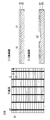
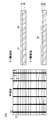
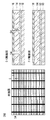
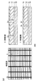
- FIG. 1A to FIG. 1F show a manufacturing process of the solar cell module 200 according to the first embodiment.
- 1A to 1F schematically show a plan view and a cross-sectional view in each step of the manufacturing process of the solar cell module 200.
- FIG. The cross-sectional view shows a cross-sectional view along line CC and a cross-sectional view along line DD in the plan view.
- a slit S1 (horizontal direction in the figure) that divides the transparent electrode 12 formed on the transparent substrate 10 by laser processing, and a slit in a direction orthogonal to the slit S1.
- S2 (vertical direction in the figure) is formed.
- the transparent substrate 10 is made of a material that transmits light having a wavelength used for photoelectric conversion in a solar cell. For example, glass, plastic, or the like is used.
- the transparent electrode 12 is transparent in which tin oxide (SnO2), zinc oxide (ZnO), indium tin oxide (ITO), etc. are doped with tin (Sn), antimony (Sb), fluorine (F), aluminum (Al), etc.
- Conductive oxide (TCO) can be used.
- a YAG laser having a wavelength of 1064 nm is preferable to use as the laser device for forming the slits S1 and S2.
- the slits S1 and S2 are formed by adjusting the power of the laser beam emitted from the laser device, irradiating from the transparent electrode 12 side, and continuously scanning in the direction of the slit S1 and the direction of the slit S2 perpendicular thereto. Can do. In addition, you may irradiate the laser for forming slit S1 and S2 from the transparent substrate 10 side.
- a multi-emission type laser device in which a plurality of laser beam emission ports are arranged at equal intervals in a direction orthogonal to the slits S1. It is preferable to use it. For example, it is preferable to use a laser device in which 2 to 5 laser beam emission ports are arranged. Thereby, in order to integrate many photovoltaic cells in series, many slits S1 can be formed at high speed.
- the processing conditions can be set even when a multi-emission laser device is used. Is easy.
- step S32 the slit S2 is blasted as shown in FIG.
- the particles 32 are sprayed from the nozzles 30 to the slits S ⁇ b> 2 where the transparent substrate 10 is exposed between the transparent electrodes 12.
- the particles 32 are preferably made of tungsten, alumina, silica, zirconium oxide or the like.
- an abrasive having a particle size of about # 1000 (# 1000).
- blasting is performed by spraying an abrasive of about 68 g / min at a frequency of 80 Hz.
- the pressure for spraying the particles 32 in the blasting process is preferably 0.1 MPa or more and 0.4 MPa or less, and more preferably 0.15 MPa or more and 0.25 MPa or less.
- Table 1 shows the processing conditions for blasting. Sample No. 7 shows a case where processing was performed using a YAG laser having a wavelength of 1064 nm as a comparative example. Table 1 also shows the evaluation of the peeled state of the transparent electrode 12 by visual observation with an optical microscope.
- the unevenness 34 is formed on the surface of the transparent substrate 10 exposed between the transparent electrodes 12 by blasting.
- an average value of a step (peak to Valley value) d between a valley and a vertex of the unevenness 34 in a cross section cut perpendicularly to the surface of the transparent substrate 10 is 0.1 ⁇ m or more and 10 ⁇ m or less. More preferably, the thickness is 1.0 ⁇ m or more and 3.0 ⁇ m or less.
- the step d can be measured with a contact-type step meter, a laser microscope, or an optical interference microscope.
- the average value of the step d is about 1 mm by scanning while making the probe of the step meter contact the surface of the transparent substrate 10 exposed between the transparent electrodes 12 as the slit S2. The average value when measured.
- the level difference d may be measured in a state after blasting, or may be measured by peeling off the back sheet of the finished solar cell module 200.
- the level difference d of the unevenness 34 is too small, the effect of increasing the contact area of the interface between the transparent substrate 10 and the photoelectric conversion unit 14 is reduced, and the effect of preventing peeling is reduced. On the other hand, if the level difference d of the unevenness 34 is too large, fine cracks due to blasting increase, which may cause generation of cracks in the substrate.
- the photoelectric conversion unit 14 is formed so as to cover the transparent electrode 12 and the slits S1 and S2.
- the photoelectric conversion unit 14 is not particularly limited, and examples thereof include an amorphous silicon (a-Si) photoelectric conversion unit, a microcrystalline silicon ( ⁇ c-Si) photoelectric conversion unit, and a tandem structure thereof.
- the photoelectric conversion unit 14 can be formed using plasma CVD or the like.
- step S36 as shown in FIG. 1D, slits S3 for dividing the photoelectric conversion unit 14 are formed by laser processing.
- the slit S3 is formed in the vicinity of the slit S1 so as to reach the surface of the transparent electrode 12 along the direction of the slit S1 at a position not overlapping the slit S1.
- the slit S3 can be formed by adjusting the power of the laser beam emitted from the laser device, irradiating from the transparent substrate 10 side, and scanning in a direction parallel to the slit S1.
- the back electrode 16 is formed so as to cover the photoelectric conversion unit 14 and the slit S3.
- the back electrode 16 is preferably a reflective metal.
- a stacked structure of a reflective metal and a transparent conductive oxide (TCO) is also preferable.
- the reflective metal silver (Ag), aluminum (Al) or the like can be used.
- the transparent conductive oxide (TCO) tin oxide (SnO2), zinc oxide (ZnO), indium tin oxide (ITO), or the like can be used.
- step S40 as shown in FIG. 1 (f), slits S4 and S5 for dividing the photoelectric conversion unit 14 and the back electrode 16 are formed by laser processing.
- the slit S4 is formed up to the surface of the transparent electrode 12 so as to divide the photoelectric conversion unit 14 and the back electrode 16 along the direction of the slits S1 and S3 in the vicinity of the slit S3 and not overlapping the slits S1 and S3. .
- the structure where the several photovoltaic cell was connected in series along the direction of slit S2 is obtained.
- the slit S5 is formed up to the surface of the transparent electrode 12 so as to divide the photoelectric conversion unit 14 and the back electrode 16 formed in the slit S2 in the region where the slit S2 is formed.
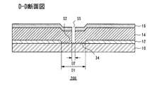
- the width D2 of the slit S5 is narrower than the width D1 of the slit S2.
- the solar cells adjacent in the direction of the slit S1 are electrically separated by the slit S5. Since the slit S5 is formed in the region where the slit S2 is formed, the laser light can be irradiated from the transparent electrode 12 side, and the slit S5 can be formed continuously when the slit S4 is formed.
- the slits S1, S3, and S4 are provided to connect adjacent solar cell groups in series, and the slits S2 and S5 are provided in parallel to the solar cell groups connected in series. Provided. Thereby, between the photovoltaic cells which adjoin along the direction of slit S1, it electrically isolates, and the structure where the photovoltaic cell group which consists of several photovoltaic cells connected in series was arranged in parallel was obtained. These solar battery cell groups are finally connected in parallel to form a solar battery module 200.
- the laser device for forming the slits S4 and S5 is preferably a YAG laser (double harmonic) having a wavelength of 532 nm.
- the slit S4 is formed by scanning in the direction parallel to the slits S1 and S3, and is continuously parallel to the slit S2.
- the slit S5 can be formed by scanning in any direction.
- the slit S2 is formed by laser processing, and then the slit S2 is blasted to form irregularities.
- the present invention is not limited to this.
- the slit S ⁇ b> 2 is not formed by laser processing, and the transparent electrode 12 in the region where the slit S ⁇ b> 2 is formed is blasted to remove the transparent electrode 12 and Concavities and convexities may be formed on the surface.
- irregularities may be formed on the surface of the transparent substrate 10 exposed to the slit S2 by wet etching using the remaining transparent electrode 12 as a mask.
- the transparent substrate 10 is a glass substrate, the wet etching method may use hydrofluoric acid.
- the adhesion at the interface between the transparent substrate 10 and the photoelectric conversion unit 14 is improved. It becomes high and peeling of the photoelectric conversion unit 14 from the transparent substrate 10 becomes difficult to occur.
- a protective layer is provided on the surface of the solar cell module 200, the adhesiveness at the interface between the protective layer formed in the slit S5 and the transparent substrate 10 is increased, and the protective layer is peeled off from the transparent substrate 10. Is less likely to occur. As a result, the environmental resistance of the solar cell module 200 can be improved, and power generation can be performed stably.
- the peeling of the photoelectric conversion unit 14 from the transparent substrate 10 is effectively suppressed by selectively performing blasting on the slit S2 that is wider than the slit S1. can do.
- the slit S5 by forming irregularities on the surface of the transparent substrate 10 exposed in the slit S2, it is possible to suppress peeling due to stress due to laser light irradiation when the subsequent slit S5 is formed.
- the pressure in blasting is 0.15 Pa or more and 0.25 Pa or less, the effect of suppressing peeling of the transparent electrode 12 from the transparent substrate 10 due to blasting becomes remarkable.
- laser processing of the slit S5 into the region of the slit S2 can be stably performed, and the manufacturing yield of the solar cell module 200 can be improved.
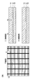
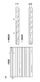
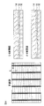
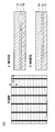
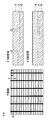
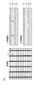
- FIG. 4A to FIG. 4F show the manufacturing process of the solar cell module 300 in the second embodiment.
- 4A to 4F schematically show a plan view and a cross-sectional view in each step of the manufacturing process of the solar cell module 300.
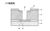
- FIG. The cross-sectional view shows a cross-sectional view along line EE and a cross-sectional view along line FF in the plan view. Note that a description of the same configurations and steps as those in the first embodiment will be omitted.
- step S50 as shown in FIG. 4A, a slit S1 (in the left-right direction in the figure) for dividing the transparent electrode 12 formed on the transparent substrate 10 is formed by laser processing.
- step S52 as shown in FIG. 4B, a slit S2 (in the vertical direction in the figure) for dividing the transparent electrode 12 formed on the transparent substrate 10 is formed by laser processing.
- the slit 2 is formed in a direction orthogonal to the slit S1.
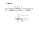
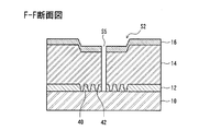
- the island of the transparent electrode 12 is formed in the slit S2 using laser light having a width less than D / 2 with respect to the entire width D of the slit S2.
- a plurality of grooves 42 are formed so that 40 is left. That is, laser light having a width of less than D / 2 is separated by the groove 42 where the surface of the transparent substrate 10 is exposed by scanning at a pitch P shorter than the full width D of the slit S2 in a direction orthogonal to the slit S1.
- An island 40 of the transparent electrode 12 is formed.
- the groove 42 is formed by using a laser beam having a width approximately equal to the width of the slit S1.
- the width d1 of the groove 42 is 5 ⁇ m or more and 100 ⁇ m or less
- the width d2 of the island 40 is 5 ⁇ m or more and 100 ⁇ m or less.
- the width d1 and the width d2 are the average value of the width of the groove 42 and the average value of the width of the island 40 measured along the direction perpendicular to the extending direction of the island 40 at the center of the film thickness of the transparent electrode 12.
- the width d1 and the width d2 can be obtained by measuring along a direction perpendicular to the extending direction of the island 40 using a contact step meter or a laser beam interferometer.
- the number of lines of the island 40 formed in the slit S2 is preferably 4 or more and 100 or less.
- the slit S2 can be formed by adjusting the power of the laser beam emitted from the laser device and irradiating from the transparent electrode 12 side. In addition, you may irradiate the laser for forming slit S2 from the transparent substrate 10 side.
- steps S54 to S58 as shown in steps S34 to S38 of the first embodiment, as shown in FIGS. 4C to 4E, the photoelectric conversion unit 14 is formed, the slit S3 is formed, Then, the back electrode 16 is formed.
- a slit S4 for dividing the photoelectric conversion unit 14 and the back electrode 16 is formed by laser processing.
- the slit S4 is formed up to the surface of the transparent electrode 12 so as to divide the photoelectric conversion unit 14 and the back electrode 16 along the direction of the slits S1 and S3 in the vicinity of the slit S3 and not overlapping the slits S1 and S3. .
- the structure where the several photovoltaic cell was connected in series along the direction of slit S2 is obtained.
- the slit S4 can be formed by adjusting the power of the laser beam emitted from the laser device, irradiating from the transparent substrate 10 side, and scanning in a direction parallel to the slits S1 and S3.
- a slit S5 for dividing the photoelectric conversion unit 14 and the back electrode 16 is formed by laser processing.
- the slit S5 is formed up to the surface of the transparent electrode 12 so as to divide the photoelectric conversion unit 14 and the back electrode 16 formed in the slit S2 in the region where the slit S2 is formed.
- the solar cells adjacent in the direction of the slit S1 are electrically separated by the slit S5.
- the laser device for forming the slit S5 uses a YAG laser with a wavelength of 1064 nm, adjusts the power of the laser beam emitted from the laser device and irradiates it from the back electrode 16 side, and scans in a direction parallel to the slit S2. By doing so, the slit S5 can be formed.
- the power of the laser beam emitted from the laser device is adjusted and irradiated from the transparent substrate 10 side, and scanned in a direction parallel to the slit S2.
- a slit S5 can be formed.
- the slit S5 may be formed by irradiating a laser beam in accordance with the position of the groove 42 formed in the slit S2, or as shown in FIG. 6B.
- the transparent electrode 12 may be formed by removing the transparent electrode 12 by irradiating it with a laser beam superimposed on a part of the island 40 of the transparent electrode 12 left in the slit S2.
- the slits S1, S3, and S4 are provided to connect adjacent solar cell groups in series, and the slits S2 and S5 are provided in parallel to the solar cell groups connected in series. Provided. Thereby, between the photovoltaic cells which adjoin along the direction of slit S1, it electrically isolates, and the structure where the photovoltaic cell group which consists of several photovoltaic cells connected in series was arranged in parallel was obtained. These solar battery cell groups are finally connected in parallel to form a solar battery module 300.
- the island 40 of the transparent electrode 12 is left in the slit S2, so that the adhesiveness in the slit S2 is improved.
- a region where the low transparent substrate 10 and the photoelectric conversion unit 14 are in direct contact is reduced.
- the adhesiveness at the interface between the transparent substrate 10 and the photoelectric conversion unit 14 in the slit S ⁇ b> 2 is increased, and the photoelectric conversion unit 14 is hardly peeled off from the transparent substrate 10.
- the slit S2 since a plurality of grooves 42 in which the transparent substrate 10 and the photoelectric conversion unit 14 are in direct contact are provided in the slit S2, even if the insulation resistance is reduced in any of the grooves 42, the slit S2 is cut by the other groove 42. The insulation between the transparent electrodes 12 of the photoelectric conversion units 14 adjacent to each other can be sufficiently maintained.
- the slit S2 is composed of the plurality of grooves 42 and the island 40, when the slit S5 is subsequently formed, peeling due to stress due to laser light irradiation can be suppressed. As a result, the laser processing of the slit S5 into the region of the slit S2 can be performed stably, and the manufacturing yield of the solar cell module 300 can be improved.
- the microcrystalline silicon layer constituting the microcrystalline silicon photoelectric conversion unit has a high film stress between the transparent substrate 10 and the substrate. Therefore, the peeling suppression effect can be remarkably enjoyed.
- the solar cell module 300 when the width of the slit S5 is formed wider than the width of the groove 42 and the slit S5 is formed so as to straddle the plurality of islands 40 and the plurality of grooves 42, the solar cell module 300 is formed.
- the protective layer is provided on the surface, the adhesion between the protective layer and the base (the island 40 and the transparent substrate 10) is increased due to the unevenness caused by the island 40 and the groove 42 formed in the slit S5.
- the protective layer is hardly peeled off. Thereby, the environmental resistance of the solar cell module 300 can be improved, and it becomes possible to generate electric power stably.
- the slit S2 is configured by the plurality of grooves 42 and the island 40, in the irradiation of the laser light when forming the subsequent slit S5, the residue caused by the photoelectric conversion unit 14 and the back electrode 16 in the groove 42 Even if this occurs, insulation between the transparent electrodes 12 of the photoelectric conversion units 14 adjacent to each other with the slit S2 sandwiched by the other groove 42 outside the region of the slit S5 can be sufficiently maintained.
Landscapes
- Photovoltaic Devices (AREA)
Abstract
【課題】太陽電池モジュールにおいて、基板と光電変換層との剥離を生じ難くさせる。 【解決手段】透明基板10上に透明電極12、光電変換ユニット14、裏面電極16を順に積層した光電変換素子を複数直列に接続し、透明電極12が第1の幅D1で除去されたスリットS2と、透明電極12が除去された領域に重なり、光電変換ユニット14及び裏面電極16が第1の幅D1以下の第2の幅D2で除去されたスリットS5と、を備え、スリットS2内の透明基板10の表面に凹凸34を設ける。
Description
本発明は、太陽電池モジュール及びその製造方法に関する。
多結晶、微結晶またはアモルファスシリコンを用いた太陽電池モジュールが知られている。特に、微結晶またはアモルファスシリコンの薄膜を積層した構造を有する太陽電池モジュールは、資源消費の観点、コストの低下の観点および効率化の観点から注目されている。
図8に、太陽電池モジュール100の基本構成の断面模式図を示す。太陽電池モジュール100は、一般的に、ガラス等の透明基板10上に透明電極12、光電変換ユニット14及び裏面電極16を積層した構造を有し、透明基板10から光を入射させることによって電力を発生させる。このような太陽電池モジュールを直列に集積するための製造方法及びパターニング装置が開示されている(例えば、特許文献1)。
図9(a)~図9(f)に、従来の太陽電池モジュール100の製造工程を示す。図9(a)~図9(f)では、太陽電池モジュール100の製造工程の各ステップにおける平面図及び断面図を模式的に示している。断面図は、平面図におけるラインA-Aに沿った断面図とラインB-Bに沿った断面図を示している。
ステップS10では、図9(a)に示すように、レーザ加工によりガラス等の透明基板10上に形成された透明電極12を分割するスリットS1、及びスリットS1に直交する方向にスリットS2を形成する。ステップS12では、図9(b)に示すように、透明電極12を被うように光電変換層となる光電変換ユニット14を成膜する。光電変換ユニット14としては、アモルファスシリコン(a-Si)光電変換ユニット、微結晶シリコン(μc-Si)光電変換ユニット又はそれらのタンデム構造が挙げられる。ステップS14では、図9(c)に示すように、レーザ加工によりスリットS1の近傍であって重ならない位置にスリットS1の方向に沿って光電変換ユニット14を分割するスリットS3を形成する。ステップS16では、図9(d)に示すように、光電変換ユニット14を被うように裏面電極16を形成する。ステップS18では、図9(e)に示すように、レーザ加工によりスリットS3の近傍であってスリットS1及びS3に重ならない位置にスリットS1,S3の方向に沿って光電変換ユニット14及び裏面電極16を分割するスリットS4を形成する。これにより、スリットS2の方向に沿って複数の太陽電池セルが直列に接続された構造が得られる。ステップS20では、図9(f)に示すように、レーザ加工によりスリットS2内に形成された光電変換ユニット14及び裏面電極16を分割するスリットS5を形成する。これにより、スリットS1の方向に沿って隣接する太陽電池セル間が電気的に分離され、直列に接続された複数の太陽電池セルからなる太陽電池セル群が複数並設された構造が得られる。そして、これら太陽電池セル群は最終的に並列に接続され、太陽電池モジュール100を構成する。
ところで、従来の太陽電池モジュールでは、直列に接続された太陽電池セルを複数の太陽電池セル群に分離するスリットS2内において光電変換層となる光電変換ユニット14が透明基板10であるガラス基板等の表面に直接接触する構成を有している。このような構成では、透明基板10と光電変換層との剥離が生じ易いという問題があった。
本発明は、基板と光電変換層との間の剥離を生じ難くし、耐久性を高めた太陽電池モジュール及びその製造方法を提供することを目的とする。
本発明の1つの態様は、基板上に第1の電極、発電層、第2の電極を順に積層した光電変換素子を複数直列に接続した太陽電池モジュールであって、第1の電極が第1の幅で除去された領域と、第1の電極が除去された領域に重なり、発電層及び第2の電極が第1の幅より狭い第2の幅で除去された領域と、を備えた分離溝を有し、分離溝内の基板表面に凹凸が設けられている、太陽電池モジュールである。
また、本発明の別の態様は、基板上に第1の電極、発電層、第2の電極を順に積層し、光電変換素子を複数直列に接続した太陽電池モジュールの製造方法であって、基板上に第1の電極を形成する第1の工程と、第1の電極の一部を第1の幅で除去した後、当該除去された領域にブラスト加工を施して基板の表面に凹凸を形成する第2の工程と、基板上に発電層及び第2の電極を順に積層する工程を含む第3の工程と、第1の電極が除去された領域に重なる領域において、第1の幅より狭い第2の幅で発電層及び第2の電極を除去する第4の工程と、を含む、太陽電池モジュールの製造方法である。
本発明の別の態様は、基板上に第1の電極、発電層、第2の電極を順に積層した光電変換素子を複数直列に接続した太陽電池モジュールであって、光電変換素子の直列接続方向に沿って第1の電極を除去した複数の溝に挟まれ第1の電極が残された島を含み、島の少なくとも一部に発電層及び第2の電極が積層されている第1のスリットと、第1のスリットが形成された領域内において第1の電極、発電層及び第2の電極が除去され、基板に達する第2のスリットと、が形成されている、太陽電池モジュールである。
また、本発明の別の態様は、基板上に第1の電極、発電層、第2の電極を順に積層し、光電変換素子を複数直列に接続した太陽電池モジュールの製造方法であって、基板上に第1の電極を形成する第1の工程と、光電変換素子が直列接続される方向に沿って第1の電極を除去して複数の溝を形成することによって、溝に挟まれ第1の電極の島が残された第1のスリットを形成する第2の工程と、島の少なくとも一部を含む第1の電極上に発電層及び第2の電極を積層する第3の工程と、第1のスリットが形成された領域内において第1の電極、発電層及び第2の電極を除去して基板に達する第2のスリットを形成する第4の工程と、を含む、太陽電池モジュールの製造方法である。
本発明によれば、基板と光電変換層との剥離を生じ難くし、耐久性及び安定性を高めた太陽電池モジュールを提供することができる。
<第1の実施の形態>
図1(a)~図1(f)に、第1の実施の形態における太陽電池モジュール200の製造工程を示す。図1(a)~図1(f)では、太陽電池モジュール200の製造工程の各ステップにおける平面図及び断面図を模式的に示している。断面図は、平面図におけるラインC-Cに沿った断面図とラインD-Dに沿った断面図を示している。
図1(a)~図1(f)に、第1の実施の形態における太陽電池モジュール200の製造工程を示す。図1(a)~図1(f)では、太陽電池モジュール200の製造工程の各ステップにおける平面図及び断面図を模式的に示している。断面図は、平面図におけるラインC-Cに沿った断面図とラインD-Dに沿った断面図を示している。
ステップS30では、図1(a)に示すように、レーザ加工により透明基板10上に形成された透明電極12を分割するスリットS1(図中、左右方向)、及びスリットS1に直交する方向にスリットS2(図中、上下方向)を形成する。透明基板10は、太陽電池において光電変換に利用される波長の光を透過する材料とし、例えば、ガラス、プラスチック等を用いる。透明電極12は、酸化錫(SnO2)、酸化亜鉛(ZnO)、インジウム錫酸化物(ITO)等に錫(Sn)、アンチモン(Sb)、フッ素(F)、アルミニウム(Al)等をドープした透明導電性酸化物(TCO)を用いることができる。
スリットS1及びS2を形成するためのレーザ装置は、波長1064nmのYAGレーザを用いることが好適である。レーザ装置から出射されるレーザビームのパワーを調整して透明電極12側から照射し、連続してスリットS1の方向及びそれに直交するスリットS2の方向に走査することによってスリットS1及びS2を形成することができる。なお、スリットS1及びS2を形成するためのレーザは、透明基板10側から照射してもよい。
また、太陽電池セルを直列に多数集積するために多数のスリットS1を形成する必要があるので、スリットS1に直交する方向にレーザビーム出射口を等間隔に複数配置したマルチ出射型のレーザ装置を用いることが好適である。例えば、2~5ヶ所のレーザビーム出射口を配置したレーザ装置を用いることが好適である。これにより、太陽電池セルを直列に多数集積するために多数のスリットS1を高速に形成することができる。なお、スリットS2の寸法は他のスリットの寸法より大きく、スリットS2の加工精度は他のスリットよりも低くてもよいので、マルチ出射型のレーザ装置を用いた場合であっても加工条件の設定は容易である。
ステップS32では、図1(b)に示すように、スリットS2をブラスト加工する。ブラスト加工では、透明電極12間に透明基板10が露出したスリットS2に対してノズル30から粒子32を吹き付ける。粒子32は、タングステン、アルミナ、シリカ、酸化ジルコニウム等を用いることが好ましい。粒子32の粒径は、研磨剤の#1000(1000番)程度のものを用いることが好適である。例えば、粒子32としてタングステンを用いた場合、68g/分程度の研磨剤を80Hzの周波数で吹き付けてブラスト加工を行う。
また、ブラスト加工において粒子32を吹き付ける圧力は0.1MPa以上0.4MPa以下とすることが好適であり、0.15MPa以上0.25MPa以下とすることがより好適である。表1は、ブラスト加工の処理条件を示す。なお、試料番号7は、比較例として波長1064nmのYAGレーザを用いて加工を行った場合を示している。また、表1には、光学顕微鏡による目視観察による透明電極12の剥離状態の評価を併せて示している。
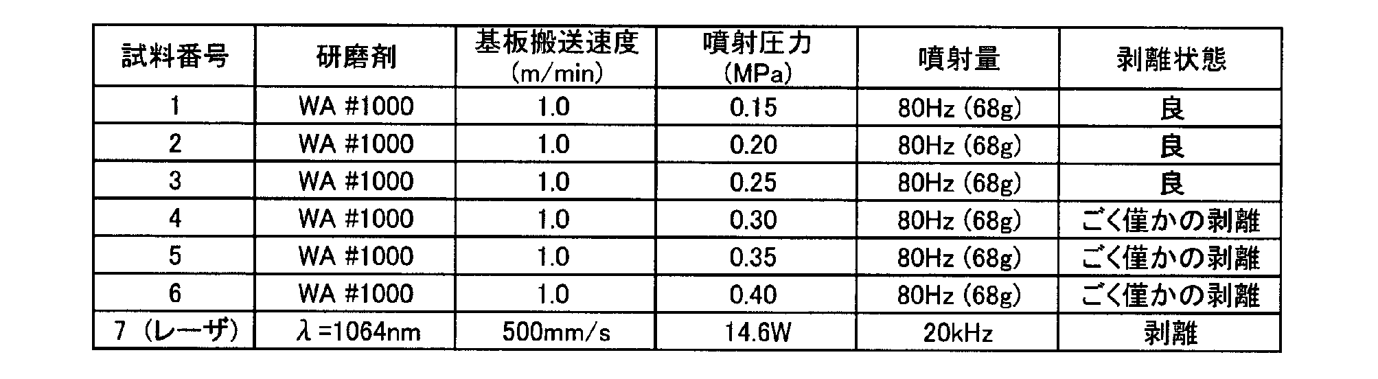
ブラスト加工において粒子32を吹き付ける圧力が低すぎる場合には、透明基板10の表面に凹凸34が形成され難くなる。一方、圧力が0.30Paを超えると、ブラスト加工による透明基板10からの透明電極12の剥離がみられる。また、微細クラックが増加し、基板の割れ等の発生の原因となるおそれがある。
ブラスト加工によって、図2の拡大断面図に示すように、透明電極12間に露出した透明基板10の表面に凹凸34が形成される。ここでは、透明基板10の表面に垂直に切断した断面において凹凸34の谷間と頂点との段差(peak to Valley値)dの平均値が0.1μm以上10μm以下とすることが好適である。さらに好ましくは、1.0μm以上3.0μm以下とすることが好適である。
なお、段差dは、接触式段差計、レーザ顕微鏡、光干渉顕微鏡で測定することができる。例えば、接触式段差計の場合には、段差dの平均値は、スリットS2として透明電極12間に露出した透明基板10の表面に段差計の探針を接触させながら走査して約1mmに亘って測定したときの平均値とする。また、段差dは、ブラスト加工後の状態で測定してもよいし、完成品の太陽電池モジュール200のバックシートを剥離して測定してもよい。
凹凸34の段差dが小さすぎると、透明基板10と光電変換ユニット14との界面の接触面積を増やす効果が減り、剥離防止の効果が小さくなる。一方、凹凸34の段差dが大きすぎると、ブラスト加工による微細クラックが増加し、基板の割れ等の発生の原因となるおそれがある。
ステップS34では、図1(c)に示すように、透明電極12及びスリットS1,S2を被うように光電変換ユニット14を成膜する。光電変換ユニット14は、特に限定されるものではないが、例えば、アモルファスシリコン(a-Si)光電変換ユニット、微結晶シリコン(μc-Si)光電変換ユニット又はそれらのタンデム構造が挙げられる。光電変換ユニット14は、プラズマCVD等を用いて形成することができる。
ステップS36では、図1(d)に示すように、レーザ加工により光電変換ユニット14を分割するスリットS3を形成する。スリットS3は、スリットS1の近傍であってスリットS1に重ならない位置にスリットS1の方向に沿って透明電極12の表面に達するように形成する。
スリットS3を形成するためのレーザ装置は、波長532nmのYAGレーザ(2倍高調波)を用いることが好適である。レーザ装置から出射されるレーザビームのパワーを調整して透明基板10側から照射し、スリットS1に平行な方向に走査することによってスリットS3を形成することができる。
ステップS38では、図1(e)に示すように、光電変換ユニット14及びスリットS3を被うように裏面電極16を形成する。裏面電極16は、反射性金属とすることが好適である。また、反射性金属と透明導電性酸化物(TCO)との積層構造とすることも好適である。反射性金属としては、銀(Ag)、アルミニウム(Al)等が使用できる。また、透明導電性酸化物(TCO)としては、酸化錫(SnO2)、酸化亜鉛(ZnO)、インジウム錫酸化物(ITO)等が使用できる。
ステップS40では、図1(f)に示すように、レーザ加工により光電変換ユニット14及び裏面電極16を分割するスリットS4及びS5を形成する。スリットS4は、スリットS3の近傍であってスリットS1及びS3に重ならない位置にスリットS1,S3の方向に沿って光電変換ユニット14及び裏面電極16を分割するように透明電極12の表面まで形成する。これにより、スリットS2の方向に沿って複数の太陽電池セルが直列に接続された構造が得られる。さらに、スリットS5は、スリットS2が形成された領域内においてスリットS2内に形成された光電変換ユニット14及び裏面電極16を分割するように透明電極12の表面まで形成する。スリットS5の幅D2は、スリットS2の幅D1よりも狭いものとする。スリットS5により、スリットS1の方向に隣接する太陽電池セル間が電気的に分離される。スリットS2が形成された領域内にスリットS5を形成するので、透明電極12側からのレーザ光の照射が可能となり、スリットS4を形成する際に連続してスリットS5を形成することができる。
上記のように、スリットS1,S3及びS4は、隣接する太陽電池セル群を直列に接続するために設けられ、スリットS2及びS5は、直列に接続された太陽電池セル群を並設するために設けられる。これにより、スリットS1の方向に沿って隣接する太陽電池セル間が電気的に分離され、直列に接続された複数の太陽電池セルからなる太陽電池セル群が複数並設された構造が得られる。そして、これら太陽電池セル群は最終的に並列に接続され、太陽電池モジュール200が構成される。
スリットS4及びS5を形成するためのレーザ装置は、波長532nmのYAGレーザ(2倍高調波)を用いることが好適である。レーザ装置から出射されるレーザビームのパワーを調整して透明基板10側から照射し、スリットS1、S3に平行な方向に走査することによってスリットS4を形成し、これに連続してスリットS2に平行な方向に走査することによってスリットS5を形成することができる。
なお、ステップS40の後に、太陽電池モジュール200の外周部分を除去する工程等を設けてもよい。また、ステップS40の後に、太陽電池モジュール200の表面を保護するためのバックシートや樹脂層を形成する工程を設けてもよい。バックシートや樹脂層は、太陽電池モジュール200の保護層として機能する。
なお、第1の実施の形態では、レーザ加工によってスリットS2を形成した後、スリットS2にブラスト加工を施して凹凸を形成したがこれに限定されるものではない。例えば、レーザ加工によってスリットS2を形成せず、スリットS2を形成する領域の透明電極12に対してブラスト加工を施して、透明電極12を除去すると共に、透明電極12の下地となる透明基板10の表面に凹凸を形成してもよい。また、レーザ加工によってスリットS2を形成した後、残された透明電極12をマスクとしてウエットエッチング法によってスリットS2に露出した透明基板10の表面に凹凸を形成してもよい。透明基板10がガラス基板である場合、ウエットエッチング法はフッ酸を用いればよい。
第1の実施の形態によれば、図3に示すように、スリットS2における透明基板10の表面に凹凸34が設けられているので、透明基板10と光電変換ユニット14との界面の密着性が高くなり、透明基板10からの光電変換ユニット14の剥離が生じ難くなる。また、太陽電池モジュール200の表面に保護層を設けた場合には、スリットS5内に形成される保護層と透明基板10との界面の密着性が高くなり、透明基板10からの保護層の剥離が生じ難くなる。これらにより、太陽電池モジュール200の耐環境性を高めることができ、安定して発電を行うことが可能となる。
ここで、透明電極12を分割するスリットにおいて、スリットS1よりも幅の広いスリットS2に対してブラスト加工を選択的に施すことにより、透明基板10からの光電変換ユニット14の剥離を効果的に抑制することができる。
また、スリットS2に露出した透明基板10の表面に凹凸を形成したことで、その後のスリットS5を形成する際、レーザ光の照射によるストレスに起因した剥離を抑制することができる。特に、ブラスト加工における圧力が0.15Pa以上0.25Pa以下において、ブラスト加工による透明基板10からの透明電極12の剥離を抑制する効果が顕著となる。この結果、スリットS2の領域内へのスリットS5のレーザ加工を安定して行うことができ、太陽電池モジュール200の製造歩留りを向上させることができる。
また、スリットS5に露出した透明基板10の表面に凹凸を形成したことで、透明基板10側から入射する光を凹凸で乱反射させることができ、本来であればスリットS5を介して透過してしまう光を、隣接する光電変換層で光電変換に寄与させることが可能になる。これにより、太陽電池モジュール200の発電効率を高めることができる。
<第2の実施の形態>
図4(a)~図4(f)に、第2の実施の形態における太陽電池モジュール300の製造工程を示す。図4(a)~図4(f)では、太陽電池モジュール300の製造工程の各ステップにおける平面図及び断面図を模式的に示している。断面図は、平面図におけるラインE-Eに沿った断面図とラインF-Fに沿った断面図を示している。なお、第1の実施の形態と同様の構成及びステップについては説明を省略する。
図4(a)~図4(f)に、第2の実施の形態における太陽電池モジュール300の製造工程を示す。図4(a)~図4(f)では、太陽電池モジュール300の製造工程の各ステップにおける平面図及び断面図を模式的に示している。断面図は、平面図におけるラインE-Eに沿った断面図とラインF-Fに沿った断面図を示している。なお、第1の実施の形態と同様の構成及びステップについては説明を省略する。
ステップS50では、図4(a)に示すように、レーザ加工により透明基板10上に形成された透明電極12を分割するスリットS1(図中、左右方向)を形成する。
ステップS52では、図4(b)に示すように、レーザ加工により透明基板10上に形成された透明電極12を分割するスリットS2(図中、上下方向)を形成する。スリット2は、スリットS1に直交する方向に形成される。
第2の実施の形態では、図5の拡大断面図に示すように、スリットS2の全幅Dに対してD/2未満の幅を有するレーザ光を用いて、スリットS2内に透明電極12の島40が残されるように複数の溝42を形成する。すなわち、D/2未満の幅を有するレーザ光をスリットS1に直交する方向に向けてスリットS2の全幅Dより短いピッチPで走査することによって、透明基板10の表面が露出する溝42によって分離された透明電極12の島40を形成する。また、本実施の形態では、溝42の形成は、スリットS1の幅と同程度の幅を有するレーザ光を用いて行っている。
溝42の幅d1は5μm以上100μm以下とし、島40の幅d2は5μm以上100μm以下とする。ここで、幅d1及び幅d2は、透明電極12の膜厚の中央において島40の延伸方向に直角な方向に沿って測定した溝42の幅の平均値及び島40の幅の平均値とする。幅d1及び幅d2は、接触段差計やレーザ光干渉計を用いて島40の延伸方向に直角な方向に沿って測定することによって求めることができる。また、光学顕微鏡又は電子顕微鏡によって、島40の延伸方向に直角な方向に沿って切断した太陽電池モジュール300の断面を観察することによって求めることができる。また、スリットS2内に形成される島40のライン数は4以上100以下とすることが好適である。
スリットS2を形成するためのレーザ装置は、波長1064nmのYAGレーザを用いることが好適である。レーザ装置から出射されるレーザビームのパワーを調整して透明電極12側から照射し、スリットS2を形成することができる。なお、スリットS2を形成するためのレーザは、透明基板10側から照射してもよい。
ステップS54~S58では、図4(c)~図4(e)に示すように、第1の実施の形態のステップS34~S38と同様に、光電変換ユニット14の成膜、スリットS3の形成、及び裏面電極16の形成が行われる。
ステップS60では、図4(f)に示すように、レーザ加工により光電変換ユニット14及び裏面電極16を分割するスリットS4を形成する。スリットS4は、スリットS3の近傍であってスリットS1及びS3に重ならない位置にスリットS1,S3の方向に沿って光電変換ユニット14及び裏面電極16を分割するように透明電極12の表面まで形成する。これにより、スリットS2の方向に沿って複数の太陽電池セルが直列に接続された構造が得られる。
スリットS4を形成するためのレーザ装置は、波長532nmのYAGレーザ(2倍高調波)を用いることが好適である。レーザ装置から出射されるレーザビームのパワーを調整して透明基板10側から照射し、スリットS1、S3に平行な方向に走査することによってスリットS4を形成することができる。
ステップS62では、図4(g)に示すように、レーザ加工により光電変換ユニット14及び裏面電極16を分割するスリットS5を形成する。スリットS5は、スリットS2が形成された領域内においてスリットS2内に形成された光電変換ユニット14及び裏面電極16を分割するように透明電極12の表面まで形成する。スリットS5により、スリットS1の方向に隣接する太陽電池セル間が電気的に分離される。
スリットS5を形成するためのレーザ装置は、波長1064nmのYAGレーザを用いて、レーザ装置から出射されるレーザビームのパワーを調整して裏面電極16側から照射し、スリットS2に平行な方向に走査することによってスリットS5を形成することができる。
また、波長532nmのYAGレーザ(2倍高調波)を用いて、レーザ装置から出射されるレーザビームのパワーを調整して透明基板10側から照射し、スリットS2に平行な方向に走査することによってスリットS5を形成することができる。
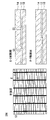
スリットS5は、図6(a)に示すように、スリットS2内に形成された溝42の位置に合わせてレーザ光を照射して形成してもよいし、図6(b)に示すように、スリットS2内に残された透明電極12の島40の一部に重畳させてレーザ光を照射し、透明電極12を除去して形成してもよい。
上記のように、スリットS1,S3及びS4は、隣接する太陽電池セル群を直列に接続するために設けられ、スリットS2及びS5は、直列に接続された太陽電池セル群を並設するために設けられる。これにより、スリットS1の方向に沿って隣接する太陽電池セル間が電気的に分離され、直列に接続された複数の太陽電池セルからなる太陽電池セル群が複数並設された構造が得られる。そして、これら太陽電池セル群は最終的に並列に接続され、太陽電池モジュール300が構成される。
なお、ステップS60の後に、太陽電池モジュール300の外周部分を除去する工程等を設けてもよい。また、ステップS60の後に、太陽電池モジュール300の表面を保護するためのバックシートや樹脂層を形成する工程を設けてもよい。バックシートや樹脂層は、太陽電池モジュール300の保護層として機能する。
第2の実施の形態によれば、図6(a)及び図6(b)に示すように、スリットS2内に透明電極12の島40が残されているので、スリットS2内において密着性の低い透明基板10と光電変換ユニット14とが直接接触している領域が小さくなる。この結果、スリットS2内における透明基板10と光電変換ユニット14との界面の密着性が高くなり、透明基板10からの光電変換ユニット14の剥離が生じ難くなる。
また、スリットS2内に透明基板10と光電変換ユニット14とが直接接触する溝42が複数設けられているため、いずれかの溝42において絶縁抵抗が小さくなったとしても他の溝42によってスリットS2を挟んで隣接する光電変換ユニット14の透明電極12間の絶縁を十分に維持することができる。
また、スリットS2を複数の溝42と島40とで構成したことで、その後のスリットS5を形成する際、レーザ光の照射によるストレスに起因した剥離を抑制することができる。この結果、スリットS2の領域内へのスリットS5のレーザ加工を安定して行うことができ、太陽電池モジュール300の製造歩留りを向上させることができる。
特に、光電変換層として微結晶シリコン(μc-Si)光電変換ユニットを用いる場合には、微結晶シリコン光電変換ユニットを構成する微結晶シリコン層が有する高い膜ストレスのために透明基板10との間の剥離が生じやすいので、剥離抑制効果を顕著に享受することができる。
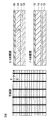
例えば、図7に示すように、スリットS5の幅を溝42の幅よりも広く形成し、スリットS5が複数の島40及び複数の溝42に跨るように形成する場合には、太陽電池モジュール300の表面に保護層を設けた際、スリットS5内に形成される島40及び溝42に起因した凹凸により保護層と下地(島40及び透明基板10)との密着性が高くなり、下地からの保護層の剥離が生じ難くなる。これにより、太陽電池モジュール300の耐環境性を高めることができ、安定して発電を行うことが可能となる。
また、スリットS2を複数の溝42と島40とで構成したことで、その後のスリットS5を形成する際のレーザ光の照射において、溝42内に光電変換ユニット14や裏面電極16に起因した残渣が生じたとしても、スリットS5の領域外の他の溝42によってスリットS2を挟んで隣接する光電変換ユニット14の透明電極12間の絶縁を十分に維持することができる。
10 透明基板、12 透明電極、14 光電変換ユニット、16 裏面電極、30 ノズル、32 粒子、34 凹凸、40 透明電極の島、42 溝、100,200,300 太陽電池モジュール。
Claims (7)
- 基板上に第1の電極、発電層、第2の電極を順に積層した光電変換素子を複数直列に接続した太陽電池モジュールであって、
前記第1の電極が第1の幅で除去された領域と、
前記第1の電極が除去された領域に重なり、前記発電層及び前記第2の電極が前記第1の幅より狭い第2の幅で除去された領域と、を備えた分離溝を有し、
前記分離溝内の前記基板表面に凹凸が設けられていることを特徴とする太陽電池モジュール。 - 請求項1に記載の太陽電池モジュールであって、
前記凹凸の段差の平均値は、0.1μm以上10μm以下であることを特徴とする太陽電池モジュール。 - 基板上に第1の電極、発電層、第2の電極を順に積層し、光電変換素子を複数直列に接続した太陽電池モジュールの製造方法であって、
前記基板上に前記第1の電極を形成する第1の工程と、
前記第1の電極の一部を第1の幅で除去した後、当該除去された領域にブラスト加工を施して前記基板の表面に凹凸を形成する第2の工程と、
前記基板上に前記発電層及び前記第2の電極を順に積層する工程を含む第3の工程と、
前記第1の電極が除去された領域に重なる領域において、前記第1の幅より狭い第2の幅で前記発電層及び前記第2の電極を除去する第4の工程と、
を含むことを特徴とする太陽電池モジュールの製造方法。 - 請求項3に記載の太陽電池モジュールの製造方法であって、
前記第2の工程では、前記ブラスト加工により前記第1の電極の一部の除去を行うことを特徴とする太陽電池モジュールの製造方法。 - 基板上に第1の電極、発電層、第2の電極を順に積層した光電変換素子を複数直列に接続した太陽電池モジュールであって、
前記光電変換素子の直列接続方向に沿って前記第1の電極を除去した複数の溝に挟まれ前記第1の電極が残された島を含み、前記島の少なくとも一部に前記発電層及び前記第2の電極が積層されている第1のスリットと、
前記第1のスリットが形成された領域内において前記第1の電極、前記発電層及び前記第2の電極が除去され、前記基板に達する第2のスリットと、
が形成されていることを特徴とする太陽電池モジュール。 - 請求項5に記載の太陽電池モジュールであって、
前記第2の電極を含む前記基板上に積層された保護層をさらに備え、
前記第2のスリットの幅は、前記溝の幅よりも広く形成されていることを特徴とする太陽電池モジュール。 - 基板上に第1の電極、発電層、第2の電極を順に積層し、光電変換素子を複数直列に接続した太陽電池モジュールの製造方法であって、
前記基板上に前記第1の電極を形成する第1の工程と、
前記光電変換素子が直列接続される方向に沿って前記第1の電極を除去して複数の溝を形成することによって、前記溝に挟まれ前記第1の電極の島が残された第1のスリットを形成する第2の工程と、
前記島の少なくとも一部を含む前記第1の電極上に前記発電層及び前記第2の電極を積層する第3の工程と、
前記第1のスリットが形成された領域内において前記第1の電極、前記発電層及び前記第2の電極を除去して前記基板に達する第2のスリットを形成する第4の工程と、
を含むことを特徴とする太陽電池モジュールの製造方法。
Priority Applications (1)
| Application Number | Priority Date | Filing Date | Title |
|---|---|---|---|
| US13/389,573 US20120145224A1 (en) | 2009-08-19 | 2010-08-17 | Solar cell module and method for manufacturing same |
Applications Claiming Priority (6)
| Application Number | Priority Date | Filing Date | Title |
|---|---|---|---|
| JP2009-190249 | 2009-08-19 | ||
| JP2009190249 | 2009-08-19 | ||
| JP2009-190688 | 2009-08-20 | ||
| JP2009190688 | 2009-08-20 | ||
| JP2010170554A JP4951699B2 (ja) | 2009-08-19 | 2010-07-29 | 太陽電池モジュール及びその製造方法 |
| JP2010-170554 | 2010-07-29 |
Publications (1)
| Publication Number | Publication Date |
|---|---|
| WO2011021615A1 true WO2011021615A1 (ja) | 2011-02-24 |
Family
ID=43607066
Family Applications (1)
| Application Number | Title | Priority Date | Filing Date |
|---|---|---|---|
| PCT/JP2010/063843 Ceased WO2011021615A1 (ja) | 2009-08-19 | 2010-08-17 | 太陽電池モジュール及びその製造方法 |
Country Status (3)
| Country | Link |
|---|---|
| US (1) | US20120145224A1 (ja) |
| JP (1) | JP4951699B2 (ja) |
| WO (1) | WO2011021615A1 (ja) |
Families Citing this family (1)
| Publication number | Priority date | Publication date | Assignee | Title |
|---|---|---|---|---|
| JP2013051257A (ja) * | 2011-08-30 | 2013-03-14 | Kyocera Corp | 光電変換装置 |
Citations (1)
| Publication number | Priority date | Publication date | Assignee | Title |
|---|---|---|---|---|
| JP2006245507A (ja) * | 2005-03-07 | 2006-09-14 | Sharp Corp | 薄膜太陽電池およびその製造方法 |
-
2010
- 2010-07-29 JP JP2010170554A patent/JP4951699B2/ja not_active Expired - Fee Related
- 2010-08-17 US US13/389,573 patent/US20120145224A1/en not_active Abandoned
- 2010-08-17 WO PCT/JP2010/063843 patent/WO2011021615A1/ja not_active Ceased
Patent Citations (1)
| Publication number | Priority date | Publication date | Assignee | Title |
|---|---|---|---|---|
| JP2006245507A (ja) * | 2005-03-07 | 2006-09-14 | Sharp Corp | 薄膜太陽電池およびその製造方法 |
Also Published As
| Publication number | Publication date |
|---|---|
| JP4951699B2 (ja) | 2012-06-13 |
| JP2011066395A (ja) | 2011-03-31 |
| US20120145224A1 (en) | 2012-06-14 |
Similar Documents
| Publication | Publication Date | Title |
|---|---|---|
| EP1583155A1 (en) | Transparent thin-film solar cell module and its manufacturing method | |
| KR100981900B1 (ko) | 광전 변환 장치 및 그 제조 방법 | |
| JP5174817B2 (ja) | 太陽電池モジュール | |
| US20150349156A1 (en) | Solar battery cell and method of manufacturing the same | |
| CN102239571B (zh) | 薄膜光电变换装置的制造方法 | |
| JP2012054457A (ja) | 太陽電池セルおよびその製造方法 | |
| KR20110031500A (ko) | 광전 변환 장치 | |
| US20140124030A1 (en) | Thin film solar cell and method for manufacturing same | |
| WO2017217219A1 (ja) | 太陽電池及びその製造方法、並びに太陽電池モジュール | |
| JP2016029675A (ja) | 薄膜太陽電池用透光性絶縁基板、及び集積型薄膜シリコン太陽電池 | |
| JP2012069566A (ja) | 薄膜太陽電池の製造方法 | |
| US8541680B2 (en) | Photovoltaic cells including peaks and methods of manufacture | |
| JP4951699B2 (ja) | 太陽電池モジュール及びその製造方法 | |
| JP2012044226A (ja) | 太陽電池モジュール | |
| TW201131791A (en) | Solar cell and method for fabricating the same | |
| JPWO2012160862A1 (ja) | 太陽電池およびその製造方法 | |
| WO2011040078A1 (ja) | 光電変換装置 | |
| JP4215608B2 (ja) | 光起電力装置 | |
| JP5134075B2 (ja) | 薄膜太陽電池の製造方法 | |
| US8330040B2 (en) | Photovoltaic cells including spaced ramps and methods of manufacture | |
| JP2010272738A (ja) | 太陽電池モジュールの製造方法 | |
| WO2011125920A1 (ja) | 光電変換装置及び光電変換装置の製造方法 | |
| JP2011035132A (ja) | 光電変換装置の製造方法、透明導電膜付き基板を備えた光電変換装置、透明導電膜付き基板、光電変換装置、及び、光電変換装置の製造装置 | |
| JP2014135446A (ja) | 光電変換装置及び光電変換装置の製造方法 | |
| WO2012042102A1 (en) | Solar cell substrate and its production method |
Legal Events
| Date | Code | Title | Description |
|---|---|---|---|
| 121 | Ep: the epo has been informed by wipo that ep was designated in this application |
Ref document number: 10809956 Country of ref document: EP Kind code of ref document: A1 |
|
| WWE | Wipo information: entry into national phase |
Ref document number: 13389573 Country of ref document: US |
|
| NENP | Non-entry into the national phase |
Ref country code: DE |
|
| 122 | Ep: pct application non-entry in european phase |
Ref document number: 10809956 Country of ref document: EP Kind code of ref document: A1 |